A Review of Charge Pump Topologies for the Power Management of IoT Nodes


Dipartimento di Ingegneria Elettrica Elettronica e Informatica (DIEEI), University of Catania, I-95125 Catania, Italy
*
Author to whom correspondence should be addressed.
Electronics 2019, 8(5), 480; https://0-doi-org.brum.beds.ac.uk/10.3390/electronics8050480
Submission received: 11 April 2019
/
Accepted: 24 April 2019
/
Published: 29 April 2019
(This article belongs to the Section Power Electronics)
Abstract
:With the aim of providing designer guidelines for choosing the most suitable solution, according to the given design specifications, in this paper a review of charge pump (CP) topologies for the power management of Internet of Things (IoT) nodes is presented. Power management of IoT nodes represents a challenging task, especially when the output of the energy harvester is in the order of few hundreds of millivolts. In these applications, the power management section can be profitably implemented, exploiting CPs. Indeed, presently, many different CP topologies have been presented in literature. Finally, a data-driven comparison is also provided, allowing for quantitative insight into the state-of-the-art of integrated CPs.
1. Introduction
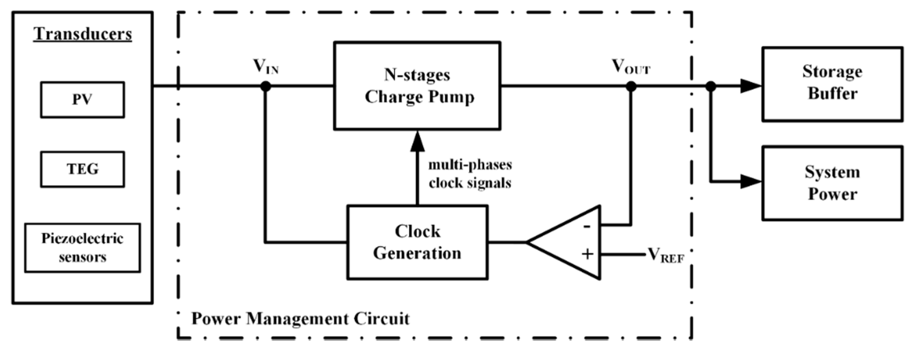
The Internet of Things (IoT) paradigm is expected to have a pervasive impact in the next years. The ubiquitous character of IoT nodes implies that they must be untethered and energy autonomous. In IoT nodes, power-autonomy is achieved by scavenging energy from the ambient using transducers, such as photovoltaic (PV) cells, thermoelectric generators (TEG), and vibration sensors [1,2,3,4]. Nevertheless, due to the heavy dependence of their output signal from the operating conditions, these transducers are often unsuitable to feed directly to the circuit where they are applied. Therefore, they employ a power management integrated circuit (PMIC) to maximize conversion efficiency.
In Figure 1 a simplified block diagram of a PMIC is shown. The input voltage, VIN, provided by an external transducer, feeds a DC-DC converter and a clock generation block. The converter is then opportunely managed to obtain a precisely stable output voltage or to optimize power consumption in function of the required load current.
The main components of a PMIC are the DC-DC converter and the clock generator. These blocks must also enable self-startup in critical conditions, i.e., low voltage and low power levels provided by the external energy harvesters [1,2,3]. The DC-DC converter can be implemented using switched inductor (SI) or switched capacitor (SC) converters. SI converters are suitable for applications requiring high power (typically larger than 100 mW), but require bulky off-chip inductors for their implementation. In low-power and low-area applications, such as IoT nodes, SC converters represent a better alternative, since they are amenable for full on-chip integration [5,6,7,8]. In literature, SC converters with a voltage gain higher than one are usually referred to as voltage multipliers or charge pumps (CPs).
Charge pumps have been traditionally adopted in nonvolatile memories and SRAMs, in which the design is driven by settling time and low area, or RF antenna switch controllers and LCD drivers, where the main design constraint is the current drivability [9,10,11]. More recently, CPs are widely used to adapt the voltage levels between two or more functional blocks and to convey the electric energy, extracted from surrounding environment, towards a storage buffer. Hence, presently their field of application includes energy-autonomous systems, such as battery-less circuits, biomedical implants and, more recently, IoT nodes [1,2,3,4,12,13,14,15,16,17,18,19,20,21,22,23]. In this latter context, the design of a PMIC based on CPs is a challenging task since it must fulfill a very low input voltage supply (few hundreds of millivolts and high-power conversion efficiency).
In literature, several works on charge pump circuits are presented. In many of them the authors focused on optimization design strategies, mainly for memory applications [24,25,26,27,28,29,30,31]. In order to further strengthen the knowledge about these important circuital blocks, this paper is aimed at reviewing the state-of-the-art review of integrated CPs, focusing on IoT applications, where the main constraints are area and power conversion efficiency. In particular, we will consider the widely adopted linear CP, due to its better general performance, as compared the other topologies, namely Fibonacci, series-parallel, exponential, and Cockcroft–Walton [5,32]. A data-driven comparison is also provided, allowing the designer to get a quantitative insight into current status of integrated CPs.
2. Charge Pump Topologies
Charge pumps fall into the class of the inductor-less DC-DC converters. They are clocked circuits implemented by switched capacitors. Therefore, they are suitable to be fully integrated and have been widely used in solid-state electronic systems since 1976 [33].
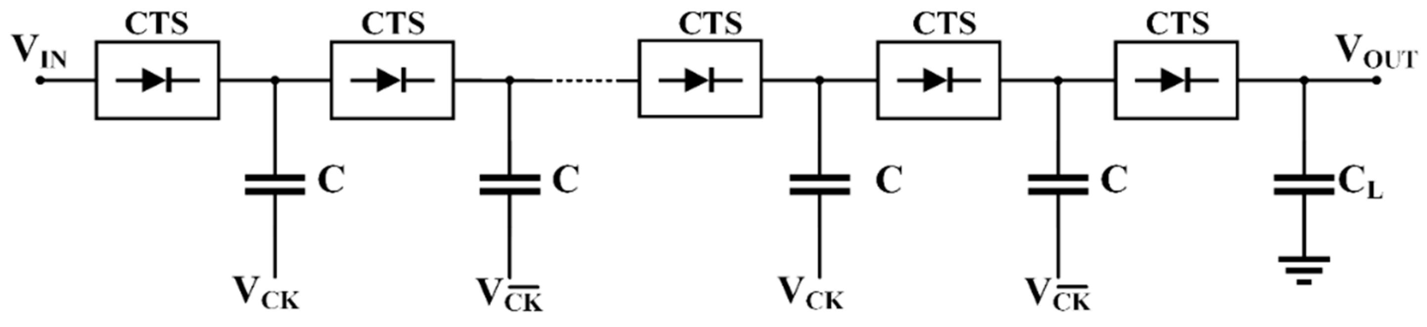
A general block scheme of an N-stage CP is shown in Figure 2, where each i-th stage is made up of a charge transfer switch (CTS) and a pumping capacitor, C. The last pair CTS and CL form the output stage. The acronym CTS was first introduced by Wu and Chang [34] to emphasize the main goal of this block, which is to irreversibly transfer charge from the input to the output. The circuit topology of the CTS constitutes the main diversification factor among the various proposed CP architectures and, of course, is an important key aspect to consider.
In the first monolithic integrated CP [33], the CTS was simply implemented with a diode-connected n-type MOSFET, which works in saturation or in the cut-off region, and the output CP steady-state voltage is given by [5,9,33]
where VCK is the clock voltage amplitude, VTH is the threshold voltages (which in turn is a function of the source-to-bulk voltage), IOUT is the load current, fCK is the clock frequency, and αT is the ratio between top parasitic capacitance and the pumping capacitance C. Although the Dickson CP is simple and allows an adequate current drivability, its efficiency and voltage gain are strongly affected by the transistor threshold voltage, as can be observed in Equation (1).
In general, the CTS is constituted by one or two main transistors, acting as a switch, and whose gates are properly driven by the following:
1. Other CP nodes;
2. Auxiliary circuits inside the CTS block.
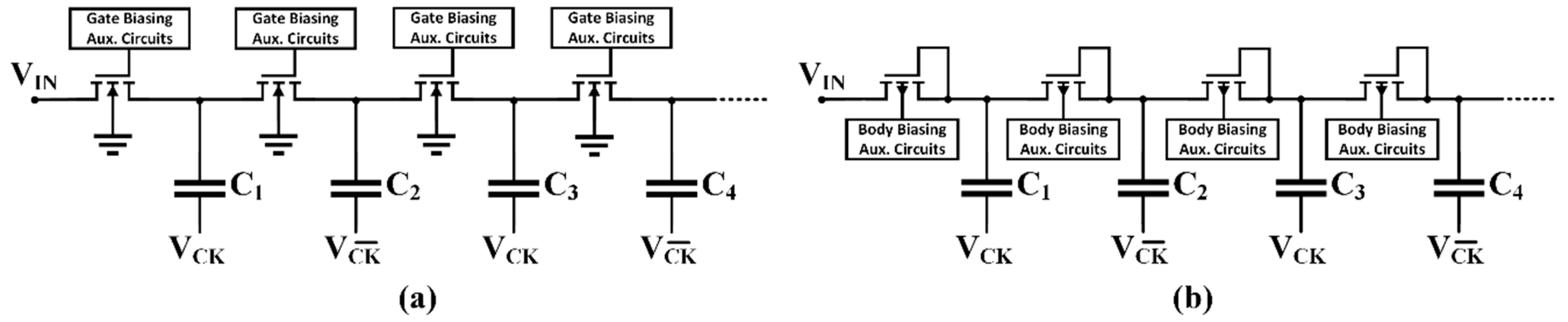
For example, an evolution of the basic Dickson topology was proposed and patented by Dickson in 1980 [35]. In this solution, reported in Figure 3a, the CTS is made up of a single NMOS transistor, with the bulk connected to ground, whose gate is connected to a forward node to increase the overdrive voltage and avoid the loss due to the transistor threshold voltage, thus allowing a reduction of the minimum supply voltage. However, its main drawback is due to the not totally turned-off CTSs. Hence, a non-negligible reverse current flows from the output to the input when the CTS is switched off, thus reducing the power conversion efficiency.
A more performing variant of the traditional Dickson CP is obtained by replacing NMOS transistors with PMOS transistors whose bulk is connected to the source, as shown in Figure 3b, which allows equal threshold voltages during turn on. Moreover, its value is increased during turn-off, thus reducing the reverse current. This solution is effective when the available technology is a standard double well and the bulk of each NMOS transistor cannot be independently controlled.
The basic idea exploited in the solutions depicted in Figure 3 can be adopted to reduce the adverse effect of threshold voltage by adopting auxiliary circuits to drive the two control terminals of the transistor, as shown in Figure 4. Indeed, gate biasing and body (or bulk) biasing techniques can be applied to better manage the transistor during on and off phases and to improve its electrical properties, such as threshold voltage and on/off resistance. These techniques are further analyzed in the following sections.
2.1. Gate Biasing Technique
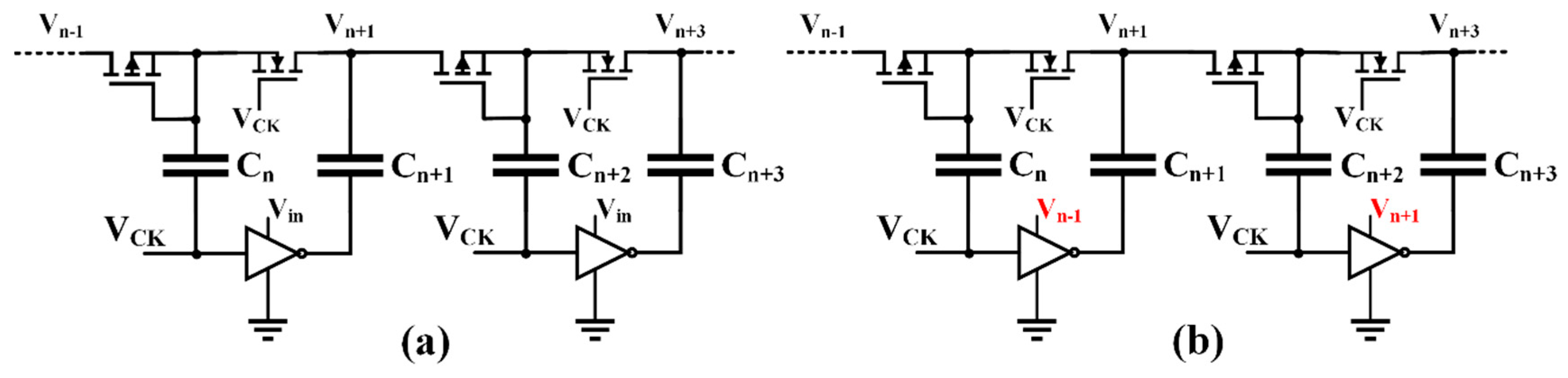
Gate biasing techniques can be classified into controlled-switch and not-controlled-switch techniques. In the first case a control signal, generated by an auxiliary circuit, is directly connected to the gate of each transistor. In the second case the gate of each transistor is connected to the node signals present in the CP itself. A CP adopting controlled-switch technique was applied for the first time on memories by D’Arrigo et al. [36] and, successively, in the complementary version by Umezawa et al. [37], to generate both negative voltages for erasing operation and positive voltage to program EEPROM cells.
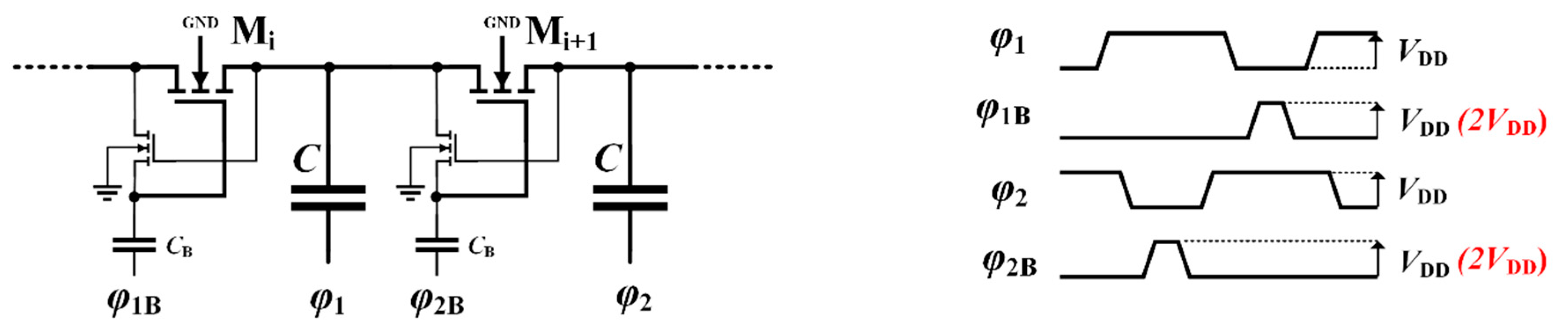
The simplified scheme and clock signal diagrams are reported in Figure 5. A four-phase non-overlapped clock is needed and a small auxiliary local boosting capacitor is added in order to boost gate voltage during the forward conduction phase. With this strategy, during the boosting phase, gate voltage stays constant and is independent of the other voltages. Consequently, the transistor Mi works in the linear region as long as its gate-to-source voltage is greater than the threshold voltage.
Despite that this circuit allows the reduction of the voltage drop across the switch, its drawback is that, during steady-state (i.e., when the pumping capacitors are charged near their maximum voltage), the MOSFET works in the sub-threshold region where its conduction properties abruptly fall-down. To overcome this drawback, the use of a boosted clock signal (red-text voltages in Figure 5) was introduced in [38]. This topology is usually named bootstrap CP. The transistor works in the triode region because the overdrive results increase by the difference between the amplitude of the two clock signals. Thus, the CP efficiency and driving capability are improved at the cost of an additional circuit to generate the boosted signal. More recently, Fuketa et al. [12] introduced a modified bootstrap CP in which phases ϕ1b and ϕ1b are switched between 0 and the output voltage to further increase performance.
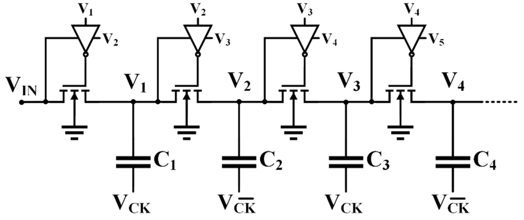
Another kind of bootstrap CP is represented by the topologies where the negated clock signal is locally implemented. A first example of this topology was introduced by Ansari et al. [39], as shown in Figure 6a, and then improved by Mondal and Paily [20,40] by adoption of the scheme depicted in Figure 6b.
A dynamic version of the basic topology in Figure 3a was introduced by Wu and Chang in [34]. A simplified schematic of this solution is reported in Figure 7. The topology of the CTS commutes from diode-connection, during the off state, to the classical static connection during the on state. In both proposals, the last switch strongly limits CP’s performance because it cannot be bootstrapped unless extra circuitry is implemented [13].
2.2. Body Biasing Technique
Focusing on the body effect of the threshold voltage, some interesting solutions employ the bias of the wells of the single transistors (n-well for PMOS and p-well for NMOS in triple-well technologies) in order to reduce VTH and allow the use of the CP in low-voltage applications. A simple body biasing solution was initially adopted by Sawada et al. [41] to implement a bootstrap all-PMOS charge pump in which the single MOSFET had source and bulk short-circuited together, as shown in Figure 8a. This connection assures that all transistors have the same threshold and minimizes reverse losses. A more complex structure was employed by Bloch et al. [42], as reported in Figure 8b, where separated p-well of the main devices were permanently kept at the lowest voltage level, within the pump stage, by means of cross-coupled transistors. Note that P-well managing avoids the parasitic bipolar junction transistors turn on.
According to the technique used to bias the source-to-body or drain-to-body junction, we can distinguish three different bias methods, as follows: forward body biasing (FBB) and backward body biasing (BBB), in which diodes are forward and backward biased, respectively, and a mixed approach called dynamic body biasing (DBB). While the earlier approach lowers the threshold voltage at the expense of an increment of the reverse current, DBB technique is more efficient, considering that during turn off, the backward-switched wells lead to an increase of the threshold voltage.
2.3. Composite Charge Pumps
In general, the CP results in a noisy block. Indeed, it has an output voltage ripple given by the following:
Thus, specs on output voltage ripple should bind the choice of a minimum value for the output capacitance. Moreover, a high input current ripple makes the use of large input by-pass capacitors necessary.
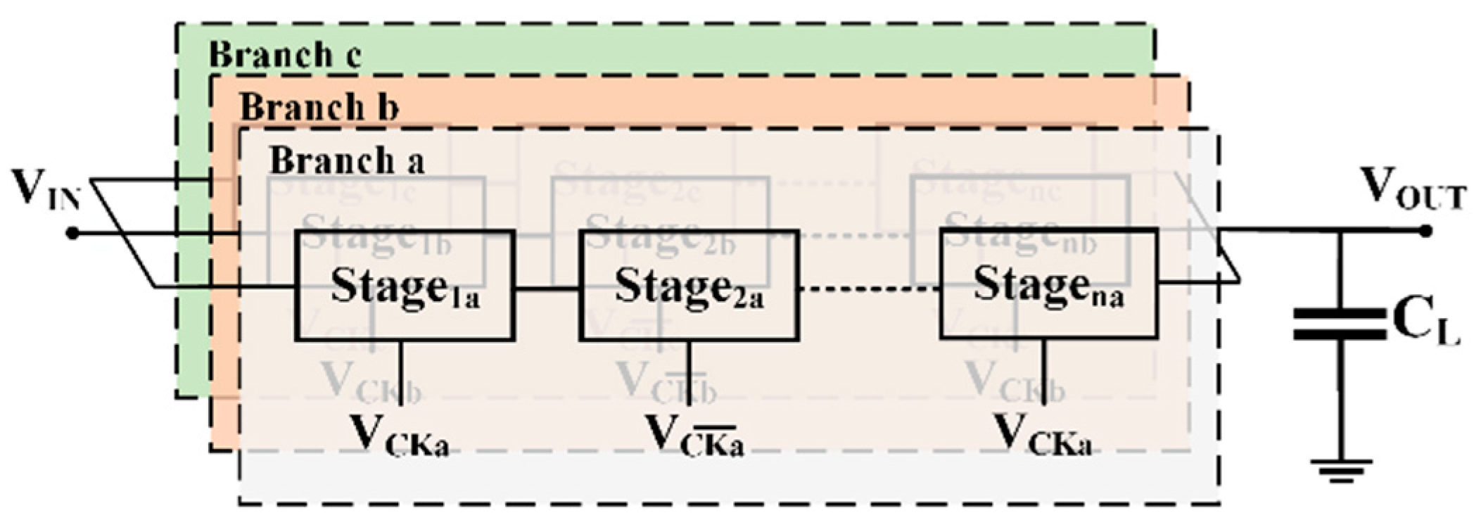
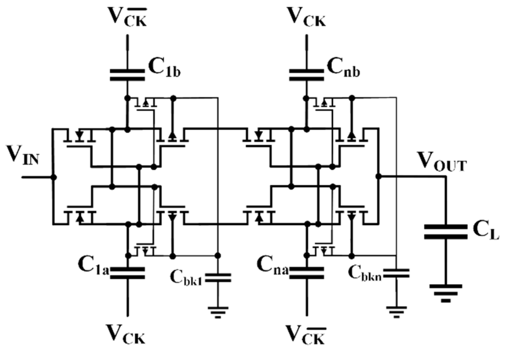
A solution to both problems is given by employing a dual-branch charge pump [44,45] as an implementation of the most generic time-interleaved charge pumps [18,46], whose simplified block diagram is reported in Figure 9. The idea behind these kinds of charge pumps is to split a single CP into two or more smaller pumps, which work in complementary time slots. This strategy increases the equivalent frequency with which the current is sunk from the power supply and delivered to the load, thus lowering the voltage ripple. Moreover, in this topology, resizing the components (switches and pumping capacitors) also allows for the increase of the maximum switching frequency limit of the converter. On the other hand, the price to pay is a higher complexity of the clock-phase generator and a greater power consumption.
More recently, Wang et al. [18] introduced the multistep split-merge charge transfer technique to get a higher power efficiency for a charge pump for solar energy harvesting. It exploits charge redistribution among the pumping capacitors of parallel CPs by means of switches inserted between capacitors belonging to different CPs.
2.4. Cross-Coupled Charge Pumps
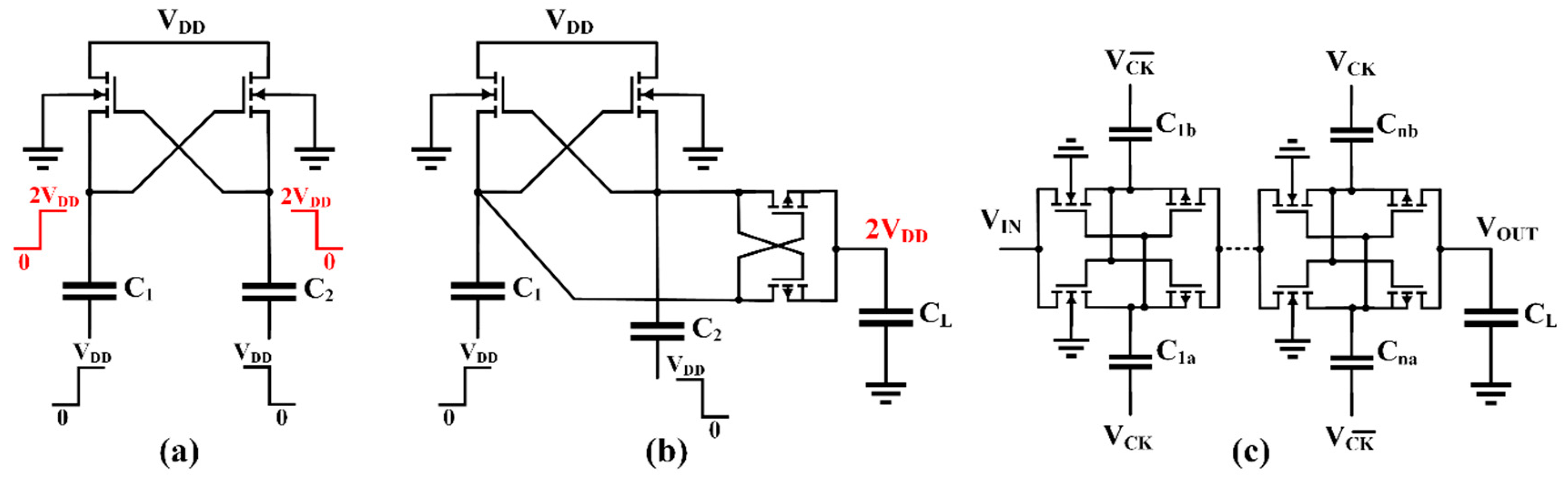
Before treating cross-coupled CPs, also referred as latched CPs, it is appropriate to introduce a particular 2-stage CP, often employed as voltage shifter or doubler. Designed for the first time by Nakagome et al. [47] as a feedback CP for a DRAM word-line driver, the well-known Nakagome’s cell, depicted in Figure 10a, is commonly adopted to generate differential doubled output voltage with zero drop across its transistors. If coupled to dual series-connected PMOS switches, a single output is obtained, as shown in Figure 10b. This combination is the basic cell of the cross-coupled CP independently proposed by Gariboldi and Pulvirenti in their quad monolithic line driver [48,49] and successively reported in [50].
Like the dual-branch structures, the latch configuration allows for reduction of the ripple and enhance charge transfer, thus improving the power efficiency. Transistors work in the linear region in on-state and are completely turned off in the opposite phase. Small auxiliary circuitry is often present with the aim of controlling the charge transfer from the input to the output. Since cross-coupled CPs are similar to dual-branch CPs, pumping capacitances of a single stage are halved, with respect to the classical Dickson CP. Therefore, transistors should be made smaller. Moreover, gate and body biasing techniques can also be applied to improve their operations. Additionally, the employment of CMOS solution should entail some limitation on the conduction level given by the series connection that includes the p-type MOSFET.
In literature many variants have been proposed for the basic topology of Figure 10c. One of these topologies was proposed by Luo et al. [51], in which pMOSFETs are bootstrapped to improve power efficiency up to 69%, with an output current of 3.5 mA and a voltage of 10.5 V. In the same year, Tsuji et al. [19] suggested a low-leakage driver for the main complementary MOSFETs of a latched CP to improve current drivability with a low input voltage (100 mV).
Another high-performance cross-coupled CP was proposed by Peng et al. [14], where bodies and gates are dynamically biased to lower the minimum supply voltage (320 mV). Its weakness resides in the need for extra stages, and complex circuits, to work-well. More effective solutions are given by Fravat et al. [52], which used two auxiliary transistors to apply the principle of bulk switching and improve PMOS current drivability and power efficiency of the Nakagome’s cell, as depicted in Figure 11.
Finally, a further improved cross-coupled CP was given by Chen et al. [53], which for the first time applied FBB on a three-stage CP, and by Kim et al. [15], which applied the dynamic body biasing on both transistors with the acquired benefits of very low start-up voltage at 150 mV and a high efficiency of 72.5%.
2.5. Clock Boosted Charge Pumps
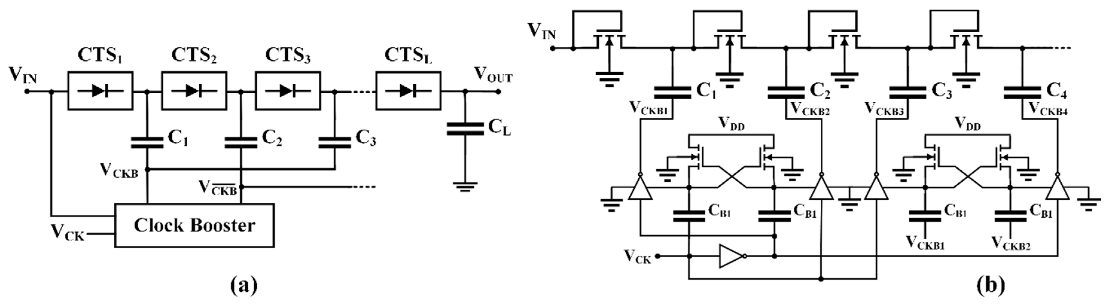
A technique allowing for the reduction of rise time or silicon area occupation, thanks to the reduction on the number of stages and using a clock boosted topology, is presented in [54,55]. These CPs use clock signals with amplitudes higher than the supply voltage, thus requiring additional blocks (other charge pumps) to boost the preexisted clock.
In [54] a clock booster was adopted to increase the steady state output voltage. In this solution, a cascade of Nakagome’s cells was used as a multi-output boosted clock, where opposite output signals of the single cell were applied, as to the single pump stage (Figure 12b). A qualitative analysis of this structure highlights that, although a reduction of stages can be obtained, the rushing fall in the driving capability, due to cascade configuration, constrains to an increase of the total capacitance values of the whole pump, nullifying the proposal’s benefits.
Recently, the authors in [55] adopted the clock booster to reduce the rise time or area occupation in CPs, with a clock amplitude doubled with respect to supply voltage, proving proper sizing strategies. In general, despite the achieved benefits, this approach is not suitable for low-power and/or energy efficient application.
2.6. Adiabatic Charge Pumps
In order to lower power consumption, an adiabatic CP has been proposed. The strategy is focused on the slow charging condition in order to reduce the energy which is not transferred to the load. In particular, the adiabatic strategy, which was originally exploited in a digital domain [56,57], is applied following two strategies. In the former, two-time step charge sharing and a particular clock scheme are used [58]. This strategy is adopted by Ulaganathan et al. [21] on a linear charge pump for energy harvesting applications. In Figure 13a, the three-stage charge pump proposed in [21] is depicted, in which two-step waveform applied on node VG allows to transfer the charge in two times, characterized by two different voltage levels. Therefore, the total transferred energy ET is given by
where Vi and Vf are the initial and final capacitor voltage levels, respectively.
The second strategy exploits the recycling of charges collected and the realization of auxiliary ground and VDD nodes, as shown in Figure 13b, where the working principle used by Keung et al. in [59] is reported. During a first time slot, thanks to the virtual ground, charges consumed by a source logic block are collected in the capacitor. Meanwhile, supply voltage feeds the target logic block. Then, when the auxiliary ground node is high, the circuits are switched and the collected charge is pumped up by the charge pump to the right-side capacitor in order to generate the auxiliary VDD, which goes to supply the target logic block. In conclusion, this approach allows about 9.95% of power consumption reduction, with only 1–2% of area penalty.
2.7. Adaptive Charge Pumps
Adaptive charge pumps, also known as reconfigurable CPs, are designed to be able to switch their number of stages [50,51] or change their voltage conversion ratio [22,60,61,62,63] in order to adaptively change current driving capability to the load or to improve very low-voltage start-up operation [23].
In this category, which also includes CPs that commute from a linear to an exponential or Fibonacci topology [64], CPs devoted to low voltage operation for microscale energy harvesting [65] and to the energy reduction in the sleep to active transition [66] were developed. Adoption of adaptative CPs must be carefully considered since, in general, the advantage obtained in terms of flexibility is paid for in circuit complexity.
3. Performance Comparison
The adoption of a specific topology among those reported in the previous section depends upon the specific application, the CMOS technology, and design specifications. Starting from the analysis of the previous section, some general guidelines are in the following.
In low-supply-voltage applications, such as energy scavenging from TEGs, gate and body control schemes could represent a good choice since they allow for lowering the minimum input voltage. In applications requiring low power consumption, energy recycling or active/idle mode transition offered by adiabatic CPs or adaptive CPs can represent an efficient solution at the expense of higher settling times and area overhead. In flash memories in which the main goal of internal DC-DC converters is to generate different voltage levels with low settling times, clock-boosted or reconfigurable CPs may represent a suitable choice.
Analysis of the reported experimental measurements of the different topologies represent an important step in the assessment of the state-of-the-art. Indeed, it may reveal additional and sometimes unexpected benefits of a particular topology. Therefore, in order to provide a deeper knowledge to the designer, performance metrics of different previously reported solutions are collected in a spreadsheet and made available online to allow independent exploration [67]. Moreover, for the sake of conciseness, a selection of 11 solutions, out of 27 in [67], targeted for energy harvesting applications, is reported in Table 1.
Except for the CP in [20], where large pumping capacitors were used to drive high current loads, in energy harvesting applications output power levels of CPs fall down in the range of tens of microwatts. Moreover, defining the power efficiency as
where Pin-CP is the input power of the CP only and Paux is the power consumption of the auxiliary circuits. The maximum η ranges from 10% to 79% (this latter value achieved by [18]). Most of the examined topologies (bootstrap or cross-coupled) exhibit a η of about 30–60%, despite that they should be inherently highly efficient. These low η values are due to the auxiliary circuits (in particular the clock generators and drivers) which can heavily affect the overall power consumption when Paux is comparable with Pin-CP.
Analysis of data reported in Table 1 reveals that the lowest minimum supply voltage is achieved by the cross-coupled topology in [2] thanks to the adoption of an auxiliary CP for startup. Unexpectedly, solutions adopting gate and body control schemes, [12,13,14,15,41,42,43], show higher minimum supply voltages, thus showing that the comparison among the different designs is not straightforward because of the different functionality and constraints required by the various applications.
A better comparison can be carried out by considering more than one parameter at the same time and also includes the voltage conversion efficiency, defined as
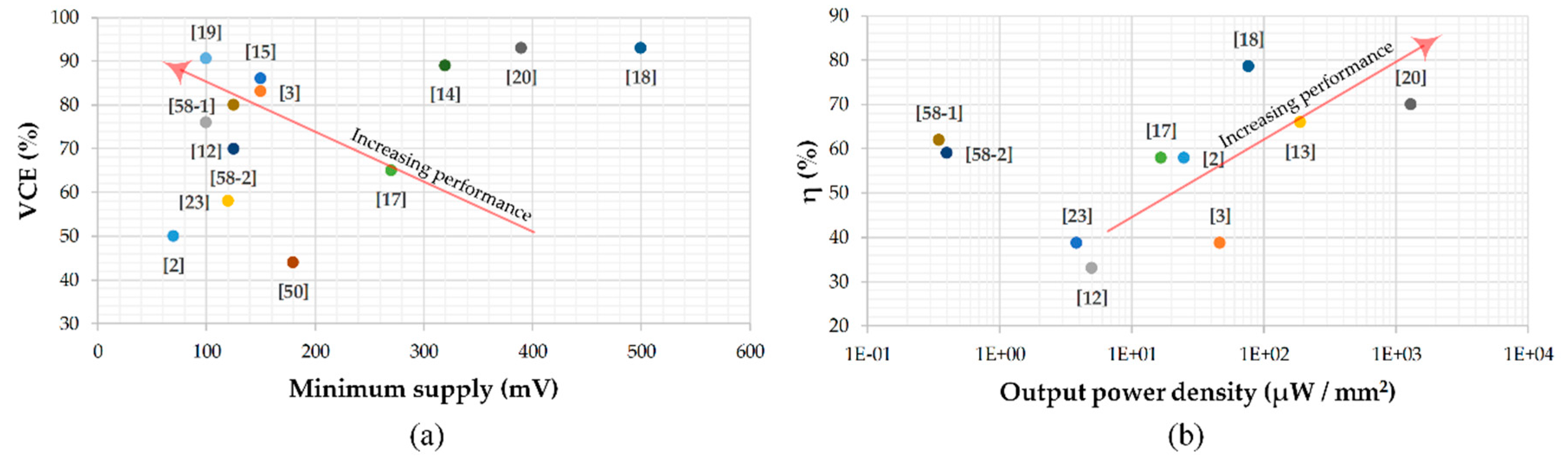
where Vout and Vout,id are the actual and ideal CP output voltage, respectively, N is the CP number of stages, and VDD is the power supply and power conversion efficiency. Such a comparison is reported in Figure 14a,b where VCE and η vs. the output power density is reported, respectively, for all the solutions in [67], which have available data to be used. By inspection of Figure 14a it is apparent that the solution reported in [2] achieves the lowest value of minimum supply voltage (75 mV), but with one of the lowest values of VCE (50%). Consequently, its overall performance appears lower than [3,15,19] which, while exhibiting higher values of minimum supply voltage (100 mV, 150 mV, and 150 mV, respectively), show much higher values of VCE (91%, 86% and 80%, respectively).
Additional information is gathered by inspection of Figure 14b. Considering the example analyzed above, it is now apparent that [2] shows better performance due to the higher value of η and output power density, while occupying much more area than [3]. However, Figure 14b shows that, from the power efficiency and power density point of view, the best performance is achieved by [13,18,20]. Note however, that [18] adopts an external clock generator and, consequently, the evaluation of the η does not take into account its additional power consumption.
4. Conclusions
In this work, a review of several solutions of linear CP topologies reported in literature is presented. After a general presentation of the topologies, the analysis is focused on the implementation of the power management section of IoT nodes. Historically, the CP topologies have evolved to cope with technological progress, thus satisfying increasingly stringent constraints given by current applications (e.g., low input voltage, high efficiency, low settling time). Quantitative comparison of the state-of-the-art reveals that the choice of a particular topology is strongly dependent upon the design constraints and the specific technology adopted.
Particular attention must be given to the design of auxiliary circuits, in particular the clock generator and drivers, whose power consumption may seriously degrade the power conversion efficiency of the overall CP.
Operation of energy harvesting applications with sub-100 mV supply voltages opens up the progress of new CPs topologies and, mainly, on the CTSs adopted. At this purpose, the use of low-threshold devices, if available, can be considered, but due to their high leakage current the possible power efficiency reduction should be taken into consideration. On the other hand, the use of standard-threshold devices working in the sub-threshold region leads to reduced capability of transfer charge. In this case, higher efficiency can be acquired at the cost of a large area of active devices.
Author Contributions
Conceptualization: A.B. and A.D.G.; original draft preparation: A.B.; writing, review and editing: A.D.G. and G.P.; formal analysis: all authors; supervision: A.D.G. and G.P.
Funding
This work was funded by University of Catania “ricerca di Ateneo-piano per la ricerca 2016/2018”.
Conflicts of Interest
The authors declare no conflict of interest.
References
- Çilingiroğlu, U.; Tar, B.; Özmen, Ç. On-Chip Photovoltaic Energy Conversion in Bulk-CMOS for Indoor Applications. IEEE Trans. Circuits Syst. I Regul. Pap. 2014, 61, 2491–2504. [Google Scholar] [CrossRef]
- Goeppert, J.; Manoli, Y. Fully Integrated Startup at 70 mV of Boost Converters for Thermoelectric Energy Harvesting. IEEE J. Solid-State Circuits 2016, 51, 1716–1726. [Google Scholar] [CrossRef]
- Yi, H.; Yin, J.; Mak, P.; Martins, R.P. A 0.032-mm20.15-V Three-Stage Charge-Pump Scheme Using a Differential Bootstrapped Ring-VCO for Energy-Harvesting Applications. IEEE Trans. Circuits Syst. Ii Express Briefs 2018, 65, 146–150. [Google Scholar] [CrossRef]
- Alioto, M. Enabling the Internet of Things: From Integrated Circuits to Integrated Systems; Springer International Publishing: Berlin/Heidelberg, Germany, 2017. [Google Scholar]
- Tanzawa, T. On-Chip High-Voltage Generator Design: Design Methodology for Charge Pumps, 2nd ed.; Springer International Publishing: Berlin/Heidelberg, Germany, 2016. [Google Scholar]
- Grasso, A.D.; Pennisi, S. Micro-scale inductorless maximum power point tracking DC-DC converter. Iet Power Electron. 2013, 6, 1634–1639. [Google Scholar] [CrossRef]
- Grasso, A.D.; Palumbo, G.; Pennisi, S. Switched-Capacitor Power Management Integrated Circuit for Autonomous Internet of Things Node. IEEE Trans. Circuits Syst. Ii Express Briefs 2018, 65, 1455–1459. [Google Scholar] [CrossRef]
- Le, H.; Sanders, S.R.; Alon, E. Design Techniques for Fully Integrated Switched-Capacitor DC-DC Converters. IEEE J. Solid-State Circuits 2011, 46, 2120–2131. [Google Scholar] [CrossRef]
- Palumbo, G.; Pappalardo, D. Charge Pump Circuits: An Overview on Design Strategies and Topologies. IEEE Circuits Syst. Mag. 2010, 10, 31–45. [Google Scholar] [CrossRef]
- Tanzawa, T. Innovation of Switched-Capacitor Voltage Multiplier: Part 1: A Brief History. IEEE Solid-State Circuits Mag. 2016, 8, 51–59. [Google Scholar] [CrossRef]
- Tanzawa, T. Innovation of Switched-Capacitor Voltage Multiplier: Part 3: State of the Art of Switching Circuits and Applications of Charge Pumps. IEEE Solid-State Circuits Mag. 2016, 8, 63–73. [Google Scholar] [CrossRef]
- Fuketa, H.; O’uchi, S.; Matsukawa, T. Fully Integrated, 100-mV Minimum Input Voltage Converter with Gate-Boosted Charge Pump Kick-Started by LC Oscillator for Energy Harvesting. IEEE Trans. Circuits Syst. Ii Express Briefs 2017, 64, 392–396. [Google Scholar] [CrossRef]
- Mahmoud, A.; Alhawari, M.; Mohammad, B.; Saleh, H.; Ismail, M. A Charge Pump Based Power Management Unit With 66%-Efficiency in 65 nm CMOS. In Proceedings of the 2018 IEEE International Symposium on Circuits and Systems (ISCAS), Florence, Italy, 27–30 May 2018; pp. 1–4. [Google Scholar]
- Peng, H.; Tang, N.; Yang, Y.; Heo, D. CMOS Startup Charge Pump With Body Bias and Backward Control for Energy HarvestingStep-Up Converters. IEEE Trans. Circuits Syst. I Regul. Pap. 2014, 61, 1618–1628. [Google Scholar] [CrossRef]
- Kim, J.; Mok, P.K.T.; Kim, C. A 0.15 V Input Energy Harvesting Charge Pump With Dynamic Body Biasing and Adaptive Dead-Time for Efficiency Improvement. IEEE J. Solid-State Circuits 2015, 50, 414–425. [Google Scholar] [CrossRef]
- Ashraf, M.; Masoumi, N. A Thermal Energy Harvesting Power Supply With an Internal Startup Circuit for Pacemakers. IEEE Trans. Very Large Scale Integr. Vlsi Syst. 2016, 24, 26–37. [Google Scholar] [CrossRef]
- Shih, Y.; Otis, B.P. An Inductorless DC–DC Converter for Energy Harvesting With a 1.2-W Bandgap-Referenced Output Controller. IEEE Trans. Circuits Syst. Ii Express Briefs 2011, 58, 832–836. [Google Scholar] [CrossRef]
- Wang, Y.; Yan, N.; Min, H.; Shi, C.-R. A High-Efficiency Split–Merge Charge Pump for Solar Energy Harvesting. IEEE Trans. Circuits Syst. Ii Express Briefs 2017, 64, 545–549. [Google Scholar] [CrossRef]
- Tsuji, Y.; Hirose, T.; Ozaki, T.; Asano, H.; Kuroki, N.; Numa, M. A 0.1–0.6 V input range voltage boost converter with low-leakage driver for low-voltage energy harvesting. In Proceedings of the 24th IEEE International Conference on Electronics, Circuits and Systems (ICECS), Batumi, Georgia, 5–8 December 2017; pp. 502–505. [Google Scholar]
- Mondal, S.; Paily, R. An Efficient On-Chip Switched-Capacitor-Based Power Converter for a Microscale Energy Transducer. IEEE Trans. Circuits Syst. Ii Express Briefs 2016, 63, 254–258. [Google Scholar] [CrossRef]
- Ulaganathan, C.; Blalock, B.J.; Holleman, J.; Britton, C.L. An ultra-low voltage self-startup charge pump for energy harvesting applications. In Proceedings of the 2012 IEEE 55th International Midwest Symposium on Circuits and Systems (MWSCAS), Boise, ID, USA, 5–8 August 2012; pp. 206–209. [Google Scholar]
- Vaisband, I.; Saadat, M.; Murmann, B. A Closed-Loop Reconfigurable Switched-Capacitor DC-DC Converter for Sub-mW Energy Harvesting Applications. IEEE Trans. Circuits Syst. Regul. Pap. 2015, 62, 385–394. [Google Scholar] [CrossRef]
- Chen, P.H.; Ishida, K.; Zhang, X.; Okuma, Y.; Ryu, Y.; Takamiya, M.; Sakurai, T. A 120-mV input, fully integrated dual-mode charge pump in 65-nm CMOS for thermoelectric energy harvester. In Proceedings of the 17th Asia and South Pacific Design Automation Conference, Sydney, NSW, Australia, 30 January–2 February 2012; pp. 469–470. [Google Scholar]
- Cataldo, G.D.; Palumbo, G. Double and triple charge pump for power IC: Dynamic models which take parasitic effects into account. IEEE Trans. Circuits Syst. I Regul. Pap. 1993, 40, 92–101. [Google Scholar] [CrossRef]
- Palumbo, G.; Barniol, N.; Bethaoui, M. Improved behavioral and design model of an Nth-order charge pump. IEEE Trans. Circuits Syst. I Fundam. Theory Appl. 2000, 47, 264–268. [Google Scholar] [CrossRef]
- di Cataldo, G.; Palumbo, G. Design of an nth order Dickson voltage multiplier. IEEE Trans. Circuits Syst. I Fundam. Theory Appl. 1996, 43, 414–418. [Google Scholar] [CrossRef]
- Palumbo, G.; Pappalardo, D.; Gaibotti, M. Charge-pump circuits: Power-consumption optimization. IEEE Trans. Circuits Syst. I Fundam. Theory Appl. 2002, 49, 1535–1542. [Google Scholar] [CrossRef]
- Boccuni, I.; Gulino, R.; Palumbo, G. Behavioral Model of Analog Circuits for Nonvolatile Memories with VHDL-AMS. Analog Integr. Circuits Signal Process. 2002, 33, 19–28. [Google Scholar] [CrossRef]
- Palumbo, G.; Pappalardo, D. Charge pump circuits with only capacitive loads: Optimized design. IEEE Trans. Circuits Syst. Ii Express Briefs 2006, 53, 128–132. [Google Scholar] [CrossRef]
- Tanzawa, T.; Tanaka, T. A dynamic analysis of the Dickson charge pump circuit. IEEE J. Solid-State Circuits 1997, 32, 1231–1240. [Google Scholar] [CrossRef]
- Tanzawa, T. An Optimum Design for Integrated Switched-Capacitor Dickson Charge Pump Multipliers With Area Power Balance. IEEE Trans. Power Electron. 2014, 29, 534–538. [Google Scholar] [CrossRef]
- Cabrini, A.; Gobbi, L.; Torelli, G. Voltage Gain Analysis of Integrated Fibonacci-Like Charge Pumps for Low Power Applications. IEEE Trans. Circuits Syst. Ii Express Briefs 2007, 54, 929–933. [Google Scholar] [CrossRef]
- Dickson, J.F. On-chip high-voltage generation in MNOS integrated circuits using an improved voltage multiplier technique. IEEE J. Solid-State Circuits 1976, 11, 374–378. [Google Scholar] [CrossRef]
- Wu, J.-T.; Chang, K.-L. MOS charge pumps for low-voltage operation. IEEE J. Solid-State Circuits 1998, 33, 592–597. [Google Scholar]
- Dickson, J.F. Voltage Multiplier Employing Clock Gated Transistor Chain. U.S. Patent US4214174A, 22 July 1980. [Google Scholar]
- D’Arrigo, S.; Imondi, G.; Santin, G.; Gill, M.; Cleavelin, R.; Spagliccia, S.; Tomassetti, E.; Lin, S.; Nguyen, A.; Shah, P.; et al. A 5 V-only 256 kbit CMOS flash EEPROM. In Proceedings of the IEEE International Solid-State Circuits Conference, 1989 ISSCC, New York, NY, USA, 15–17 February 1989; pp. 132–133. [Google Scholar]
- Umezawa, A.; Atsumi, S.; Kuriyama, M.; Banba, H.; Imamiya, K.I.; Naruke, K.; Yamada, S.; Obi, E.; Oshikiri, M.; Suzuki, T.; et al. A 5-V-only operation 0.6- mu m flash EEPROM with row decoder scheme in triple-well structure. IEEE J. Solid-State Circuits 1992, 27, 1540–1546. [Google Scholar] [CrossRef]
- Atsumi, S.; Kuriyama, M.; Umezawa, A.; Banba, H.; Naruke, K.; Yamada, S.; Ohshima, Y.; Oshikiri, M.; Hiura, Y.; Yamane, T.; et al. A 16-Mb flash EEPROM with a new self-data-refresh scheme for a sector erase operation. IEEE J. Solid-State Circuits 1994, 29, 461–469. [Google Scholar] [CrossRef]
- Ansari, M.A.; Ahmad, W.; Signell, S.R. Single clock charge pump designed in 0.35µm technology. In Proceedings of the 18th International Conference Mixed Design of Integrated Circuits and Systems, Gliwice, Poland, 16–18 June 2011; pp. 552–556. [Google Scholar]
- Mondal, S.; Paily, R.P. A strategy to enhance the output voltage of a charge pump circuit suitable for energy harvesting. In Proceedings of the 2013 Annual International Conference on Emerging Research Areas and 2013 International Conference on Microelectronics, Kanjirapally, India, 4–6 June 2013; pp. 1–5. [Google Scholar]
- Sawada, K.; Sugawara, Y.; Masui, S. An on-chip high-voltage generator circuit for EEPROMs with a power supply voltage below 2 V. In Proceedings of the Symposium on VLSI Circuits, Kyoto, Japan, 8–10 June 1995; pp. 75–76. [Google Scholar]
- Bloch, M.; Lauterbauch, C.; Weber, W. High efficiency charge pump circuit for negative high voltage generation at 2 V supply voltage. In Proceedings of the 24th European Solid-State Circuits Conference, The Hague, The Netherlands, 22–24 September 1998; pp. 100–103. [Google Scholar]
- Zhang, X.; Lee, H. Gain-Enhanced Monolithic Charge Pump With Simultaneous Dynamic Gate and Substrate Control. IEEE Trans. Very Large Scale Integr. Vlsi Syst. 2013, 21, 593–596. [Google Scholar] [CrossRef]
- Kleveland, B. Multi-Stage Charge Pump. Patent US6486728B2, 26 November 2002. [Google Scholar]
- New, L.F.; Aziz, Z.A.b.A.; Leong, M.F. A low ripple CMOS charge Pump for low-voltage application. Proc. ICIAS 2012, 2, 784–789. [Google Scholar]
- Ma, D.; Bondade, R. Reconfigurable Switched—Capacitor Power Converters; Springer: New York, NY, USA.
- Nakagome, Y.; Tanaka, H.; Takeuchi, K.; Kume, E.; Watanabe, Y.; Kaga, T.; Kawamoto, Y.; Murai, F.; Izawa, R.; Hisamoto, D.; et al. An experimental 1.5-V 64-Mb DRAM. IEEE J. Solid-State Circuits 1991, 26, 465–472. [Google Scholar] [CrossRef]
- Gariboldi, R.; Pulvirenti, F. A monolithic quad line driver for industrial applications. IEEE J. Solid-State Circuits 1994, 29, 957–962. [Google Scholar] [CrossRef]
- Gariboldi, R.; Pulvirenti, F. A 70 m/spl Omega/ intelligent high side switch with full diagnostics. IEEE J. Solid-State Circuits 1996, 31, 915–923. [Google Scholar] [CrossRef]
- Ker, M.-D.; Chen, S.-L.; Tsai, C.-S. Design of charge pump circuit with consideration of gate-oxide reliability in low-voltage CMOS processes. IEEE J. Solid-State Circuits 2006, 41, 1100–1107. [Google Scholar] [CrossRef]
- Luo, Z.; Ker, M.; Cheng, W.; Yen, T. Regulated Charge Pump with New Clocking Scheme for Smoothing the Charging Current in Low Voltage CMOS Process. IEEE Trans. Circuits Syst. I Regul. Pap. 2017, 64, 528–536. [Google Scholar] [CrossRef]
- Favrat, P.; Deval, P.; Declercq, M.J. A high-efficiency CMOS voltage doubler. IEEE J. Solid-State Circuits 1998, 33, 410–416. [Google Scholar] [CrossRef]
- Chen, P.H.; Ishida, K.; Zhang, X.; Okuma, Y.; Ryu, Y.; Takamiya, M.; Sakurai, T. 0.18-V input charge pump with forward body biasing in startup circuit using 65nm CMOS. In Proceedings of the IEEE Custom Integrated Circuits Conference 2010, San Jose, CA, USA, 19–22 September 2010; pp. 1–4. [Google Scholar]
- Huang, W.C.; Cheng, J.C.; Liou, P.C.; Liou, C.W. A charge pump circuit using multi-staged voltage doubler clock scheme. In Proceedings of the 2007 Internatonal Conference on Microelectronics, Cairo, Egypt, 29–31 December 2007; pp. 317–320. [Google Scholar]
- Ballo, A.; Grasso, A.D.; Giustolisi, G.; Palumbo, G. Optimized charge pump with clock booster for reduced rise time or silicon area. IEEE Tran. Circuits Syst. II: Express Briefs 2019, in press. [Google Scholar] [CrossRef]
- Athas, W.C.; Svensson, L.J.; Koller, J.G.; Tzartzanis, N.; Chou, E.Y.-C. Low-power digital systems based on adiabatic-switching principles. IEEE Trans. Very Large Scale Integr. Vlsi Syst. 1994, 2, 398–407. [Google Scholar] [CrossRef]
- Alioto, M.; Palumbo, G. Performance evaluation of adiabatic gates. IEEE Trans. Circuits Syst. Fundam. Theory Appl. 2000, 47, 1297–1308. [Google Scholar]
- Lauterbach, C.; Weber, W.; Romer, D. Charge sharing concept and new clocking scheme for power efficiency and electromagnetic emission improvement of boosted charge pumps. IEEE J. Solid-State Circuits 2000, 35, 719–723. [Google Scholar] [CrossRef]
- Keung, K.; Manne, V.; Tyagi, A. A Novel Charge Recycling Design Scheme Based on Adiabatic Charge Pump. IEEE Trans. Very Large Scale Integr. Vlsi Syst. 2007, 15, 733–745. [Google Scholar] [CrossRef]
- Tanzawa, T.; Tanaka, T.; Takeuchi, K.; Nakamura, H. Circuit techniques for a 1.8-V-only NAND flash memory. IEEE J. Solid-State Circuits 2002, 37, 84–89. [Google Scholar] [CrossRef]
- Palumbo, G.; Pappalardo, D.; Gaibotti, M. Charge pump with adaptive stages for non-volatile memories. IEEE Proc. Circuits Devices Syst. 2006, 153, 136–142. [Google Scholar] [CrossRef]
- Zhang, X.; Lee, H. An Efficiency-Enhanced Auto-Reconfigurable 2-/3-SC Charge Pump for Transcutaneous Power Transmission. IEEE J. Solid-State Circuits 2010, 45, 1906–1922. [Google Scholar] [CrossRef]
- Beck, Y.; Singer, S. Capacitive Transposed Series-Parallel Topology With Fine Tuning Capabilities. IEEE Trans. Circuits Syst. I Regul. Pap. 2011, 58, 51–61. [Google Scholar] [CrossRef]
- Ueno, F.; Inoue, T.; Oota, I.; Harada, I. Emergency power supply for small computer systems. In Proceedings of the IEEE International Sympoisum on Circuits and Systems, Singapore, 11–14 June 1991; pp. 1065–1068. [Google Scholar]
- Gupta, A.K.; Joshi, A.; Gajare, V.; Ghanshyam, H.S.; Dutta, A. Power efficient reconfigurable charge pump for micro scale energy harvesting. In Proceedings of the 2013 IEEE Asia Pacific Conference on Postgraduate Research in Microelectronics and Electronics (PrimeAsia), Visakhapatnam, India, 19–21 December 2013; pp. 73–76. [Google Scholar]
- Alioto, M.; Consoli, E.; Rabaey, J.M. ‘EChO’ Reconfigurable Power Management Unit for Energy Reduction in Sleep-Active Transitions. IEEE J. Solid-State Circuits 2013, 48, 1921–1932. [Google Scholar] [CrossRef]
- Ballo, A.; Grasso, A.D.; Palumbo, G. Linear Charge Pumps Survey. Available online: https://bit.ly/2Ieicoe (accessed on 11 April 2019).
Figure 1.
Simplified block diagram of a charge pump (CP)-based energy harvesting power management integrated circuit (PMIC).
Figure 1.
Simplified block diagram of a charge pump (CP)-based energy harvesting power management integrated circuit (PMIC).

Figure 2.
Simplified scheme of a linear Dickson charge pump.

Figure 3.
Dickson charge pump: (a) NMOS enhanced version [35]; (b) all-PMOS implementation.
Figure 3.
Dickson charge pump: (a) NMOS enhanced version [35]; (b) all-PMOS implementation.

Figure 4.
Simplified schematic of (a) gate biasing technique and (b) bulk biasing technique.

Figure 5.
Charge transfer switch (CTS) in bootstrap CP, proposed by D’Arrigo et al. [36], and time diagram of the clock phases.
Figure 5.
Charge transfer switch (CTS) in bootstrap CP, proposed by D’Arrigo et al. [36], and time diagram of the clock phases.

Figure 6.
Bootstrap CP with locally generated negated clock signal, (a) conventional [39] and (b) improved [20].

Figure 7.
Block scheme of the charge pump proposed by Wu and Chang [34].
Figure 7.
Block scheme of the charge pump proposed by Wu and Chang [34].

Figure 8.
(a) Body biasing technique applied by Sawada et al. [41] with PMOS transistors and (b) by Bloch et al. [42] with NMOS transistors.

Figure 9.
Composite charge pump.

Figure 10.
Nakagome’s cell block scheme (a) without and (b) with PMOS switches, and (c) a cross-coupled charge pump.
Figure 10.
Nakagome’s cell block scheme (a) without and (b) with PMOS switches, and (c) a cross-coupled charge pump.

Figure 11.
Cross-coupled CP with bulk switching [52].
Figure 11.
Cross-coupled CP with bulk switching [52].

Figure 12.
Clock boosted charge pumps, (a) simplified block scheme and (b) multi-stage clock [54].
Figure 12.
Clock boosted charge pumps, (a) simplified block scheme and (b) multi-stage clock [54].

Figure 13.
Adiabatic charge pumps, (a) two-time step charge sharing [21] and (b) charge recycling block scheme [59].

Figure 14.
Performance comparison, (a) VCE versus minimum input voltage and (b) η versus output power density.
Figure 14.
Performance comparison, (a) VCE versus minimum input voltage and (b) η versus output power density.


Table 1.
Comparison of different charge pumps.
| Ref. | [2] | [3] | [12] | [13] | [14] | [15] | [17] | [18] | [20] | [58] a | [23] | |
|---|---|---|---|---|---|---|---|---|---|---|---|---|
| Topology | Cross-coupled/composite | Cross-coupled | Bootstrap | Dickson-with DGB | Cross-coupled with BGB | Cross-coupled DBB | Bootstrap | Bootstrap | Bootstrap | Adiabatic | Adaptive | |
| No. Of Stages | 6 pararallel 24 | 3 | 10 | 4 | 6 | 3 | 3 | 5 | 1 | 3 | 7 | 10 |
| Aux. Circuit | Start-up circuit | Clock booster 3x | Clock booster 2x | Dynamic G control | Backward G Biasing | Dynamic B control | - | Split-merge four-branches | - | Low-threshold diode in every CTS | - | |
| Technology (nm) | 130 | 65 | 65 | 65 | 180 | 130 | 130 | 130 | 180 | 130 | 65 | |
| Min. Supply (mV) | 70 | 150 | 100 | 550 | 320 | 150 | 270 | 500 | 390 | 125 | 120 | |
| Clock Frequency (MHz) | 0.040 | 15.2 | 10 | 1.8 | 0.45 | 0.25 | 0.8 | 2.5 | 23 | 0.360 | 1 | |
| Total Pumping Cap. (pF) | 46.08 | 22.5 | 1001 | 160 | 288 | 36,000 b | 150 | 310 | 500 | 96 | 224 | 286 |
| Load Cap. (pF) | 10,000 b | 30 | 100 | 400 | 50.7 | 10,000 b | 500 | 800 | 4000 b | 100 | - | |
| Load Current at Peak η (µA) | 12 | 1.74 | 0.76 | 10 | - | 21 | 5 | 30 | 620 | 0.1 | 3.9 | |
| Max Output Power (μW) | 15 | 1.5 | 6.6 | 4.7 | - | 10.5 | 7 | 75 | 620 | 0.061 | 0.035 | 3 |
| Peak VCE (%) | 50 | 80 | 76 | 96 | 89 | 86 | 65 | 93 | 93 | 70 | 80 | 58 |
| Peak η (%) | 58 | 38.8 | 33 | 66 | - | 34 c | 58 | 78.6 c | 76 | 59 | 62 | 38.8 |
| Area (mm2) | 0.6 | 0.032 | 1.32 | 0.17 | 0.14 mm2 | 0.066 b | 0.42 | 0.98 | 0.48 | 0.15 | 0.1 | 0.78 |
a simulations; b off-chip capacitors; c external clock generator
© 2019 by the authors. Licensee MDPI, Basel, Switzerland. This article is an open access article distributed under the terms and conditions of the Creative Commons Attribution (CC BY) license (http://creativecommons.org/licenses/by/4.0/).
Share and Cite
MDPI and ACS Style
Ballo, A.; Grasso, A.D.; Palumbo, G. A Review of Charge Pump Topologies for the Power Management of IoT Nodes. Electronics 2019, 8, 480. https://0-doi-org.brum.beds.ac.uk/10.3390/electronics8050480
AMA Style
Ballo A, Grasso AD, Palumbo G. A Review of Charge Pump Topologies for the Power Management of IoT Nodes. Electronics. 2019; 8(5):480. https://0-doi-org.brum.beds.ac.uk/10.3390/electronics8050480
Chicago/Turabian StyleBallo, Andrea, Alfio Dario Grasso, and Gaetano Palumbo. 2019. "A Review of Charge Pump Topologies for the Power Management of IoT Nodes" Electronics 8, no. 5: 480. https://0-doi-org.brum.beds.ac.uk/10.3390/electronics8050480
Note that from the first issue of 2016, this journal uses article numbers instead of page numbers. See further details here.