Article

Electrospinning for the Modification of 3D Objects for the Potential Use in Tissue Engineering

1
Faculty of Engineering and Mathematics, Bielefeld University of Applied Sciences, 33619 Bielefeld, Germany
2
Department of Physical and Biophysical Chemistry (PC III), Faculty of Chemistry, Bielefeld University, 33615 Bielefeld, Germany
*
Author to whom correspondence should be addressed.
Submission received: 29 April 2022 / Revised: 25 May 2022 / Accepted: 26 May 2022 / Published: 29 May 2022
(This article belongs to the Special Issue 10th Anniversary of Technologies—Recent Advances and Perspectives)

Abstract

:
Electrospinning is often investigated for biotechnological applications, such as tissue engineering and cell growth in general. In many cases, three-dimensional scaffolds would be advantageous to prepare tissues in a desired shape. Some studies thus investigated 3D-printed scaffolds decorated with electrospun nanofibers. Here, we report on the influence of 3D-printed substrates on fiber orientation and diameter of a nanofiber mat, directly electrospun on conductive and isolating 3D-printed objects, and show the effect of shadowing, taking 3D-printed ears with electrospun nanofiber mats as an example for potential and direct application in tissue engineering in general.

1. Introduction

Electrospinning enables the production of nanofibers in a relatively fast and simple way. Generally, a polymer solution or melt is inserted into a strong electric field between two electrodes, one of which is typically the needle through which the spinning solution is pressed, or a wire coated with the spinning solution [1,2]. The field leads to the formation of Taylor cones from which a polymer jet is extruded towards the counter-electrode. The spiraling shape of this jet results in strong elongation while the solvent is evaporated, until ultrathin nanofibers are deposited on the counter-electrode or a substrate that shields the counter-electrode [3,4,5].
The fiber orientation on the substrate depends on the collector. A static collector, as is mostly used in wire-based electrospinning, usually leads to arbitrary fiber orientations [6,7]. For several applications, it can be supportive to use roughly parallel oriented fibers. This can be reached, e.g., with a fast-rotating cylinder as collector [8,9]. Another possibility to prepare mats of aligned nanofibers is given by adding dielectric or conductive areas to the substrate, which deform the electric field and in this way allow for the tailoring of the position of the deposited nanofibers, as well as their orientation to a certain amount [10,11,12].
Such oriented nanofibers are often supportive for oriented cell growth and increased cell proliferation, both of which are important factors in tissue engineering [13,14]. Another important factor is the material of the electrospun nanofibers. Many biomaterials, such as gelatin, are water-soluble and thus have the disadvantage that they need an additional crosslinking step after spinning before they can be used in a fluid medium [15,16]. Other polymers need toxic solvents, which makes a sophisticated post-treatment necessary to avoid reducing the biocompatibility of the nanofiber mats [17,18]. Only few water-stable polymers can be electrospun from the low-toxic solvent dimethyl sulfoxide (DMSO) [19], amongst them poly(acrylonitrile) (PAN) [20,21]. While pure PAN does not serve as an ideal substrate for cell adhesion and proliferation, water-stable blends of PAN with gelatin, maltodextrin, casein, etc. can be used to support cell growth [22,23].
Here we report on electrospinning PAN nanofiber mats on different 3D printed shapes, prepared from various polymers, some of which have conductive properties. Generally, the combination of 3D-printed shapes with an electrospun nanostructure was reported to be an interesting method to combine the desired morphology, mimicking the extracellular matrix, with a desired macroscopic shape [24,25,26].
Opposite to a previous study in which nanofibers were electrospun on a flat 3D-printed structure [27], here higher and partly irregular shapes are investigated, especially regarding shadowing effects, taking 3D-printed ears with nanofiber mats as an example. Optical investigations reveal strongly different fiber orientations, depending on the shape and the material of the 3D-printed substrates.

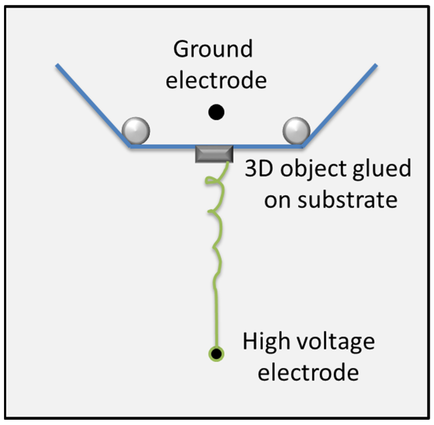
2. Materials and Methods

Electrospinning was performed on the wire-based electrospinning machine Nanospider Lab (Elmarco, Liberec, Czech Republic) applying the following unchanged spinning parameters during the experiments: nozzle diameter 0.9 mm; distance between electrode and substrate 240 mm; carriage speed 100 mm/s; the substrate was not moved. The temperature in the spinning chamber was 22–23 °C, the relative humidity 32–33%. The varying spinning parameters are given in Table 1.
The spinning solutions were prepared from 13–16% PAN (X-PAN, Dralon, Dormagen, Germany) and 2–5% Dextran 500 (for biochemistry, 500 kDa, purchased from Carl Roth GmbH & Co. KG, Karlsruhe, Germany) dissolved in DMSO (min 99.9%, S3 chemicals, Bad Oeynhausen, Germany) by stirring for 24 h under ambient conditions.
The following 3D-printing materials were investigated:
-
Filaflex 82A (Recreus, Elda, Spain)
-
Conductive PLA (Proto-pasta, Vancouver, Canada)
-
XT-CF20 (Colorfabb, Belfeld, The Netherlands)
-
Bronzefill (Colorfabb, Belfeld, The Netherlands)
-
Growlay brown (Lay-Filaments, Cologne, Germany)
-
Carbon X2–85 (3DXTech, Grand Rapids, MI, USA)
-
CarbonFil (Formfutura, Nijmegen, The Netherlands)
-
Poly(lactic acid) (PLA) (Filamentworld, Neu-Ulm, Germany)
Only the conductive PLA shows a measurable conductivity (R~200 Ω/cm); the others partly include conductive carbon fibers, etc., but apparently without forming sufficient percolation paths.
3D printing was performed using an Orcabot XXL (Prodim, The Netherlands) with a nozzle diameter of 0.4 mm, nozzle temperature of 210 °C, printing bed temperature of 60 °C, layer thickness of 0.2 mm and 100% infill (linear).
The ear model was taken from Thingiverse (https://www.thingiverse.com/thing:304657, created by addamay123, published under a CC-BY-SA license, accessed on 7 March 2022).
All 3D-printed specimens and 3D-printing filaments were mounted below the standard polypropylene substrate, as depicted in Figure 1.
The following samples were prepared, varying spinning parameters and 3D printed parts:
The morphology of the samples was investigated by a confocal laser scanning microscopy (CLSM) VK-8710 (Keyence, Neu-Isenburg, Germany). Exemplary images were taken by a scanning electron microscope (SEM) FEI XL30 ESEM (Philips, Amsterdam, The Netherlands), after sputtering the samples with palladium. Macroscopic images were taken by a Sony Cybershot DSC-RX100 IV camera.

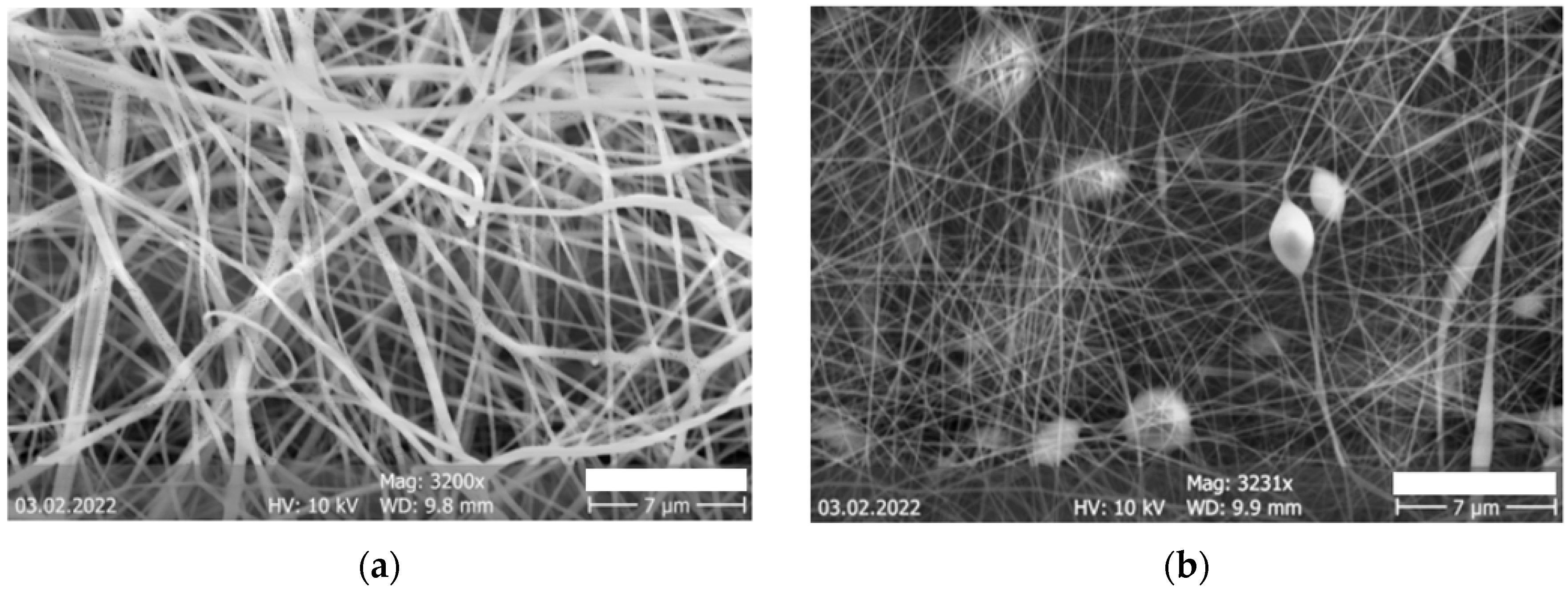
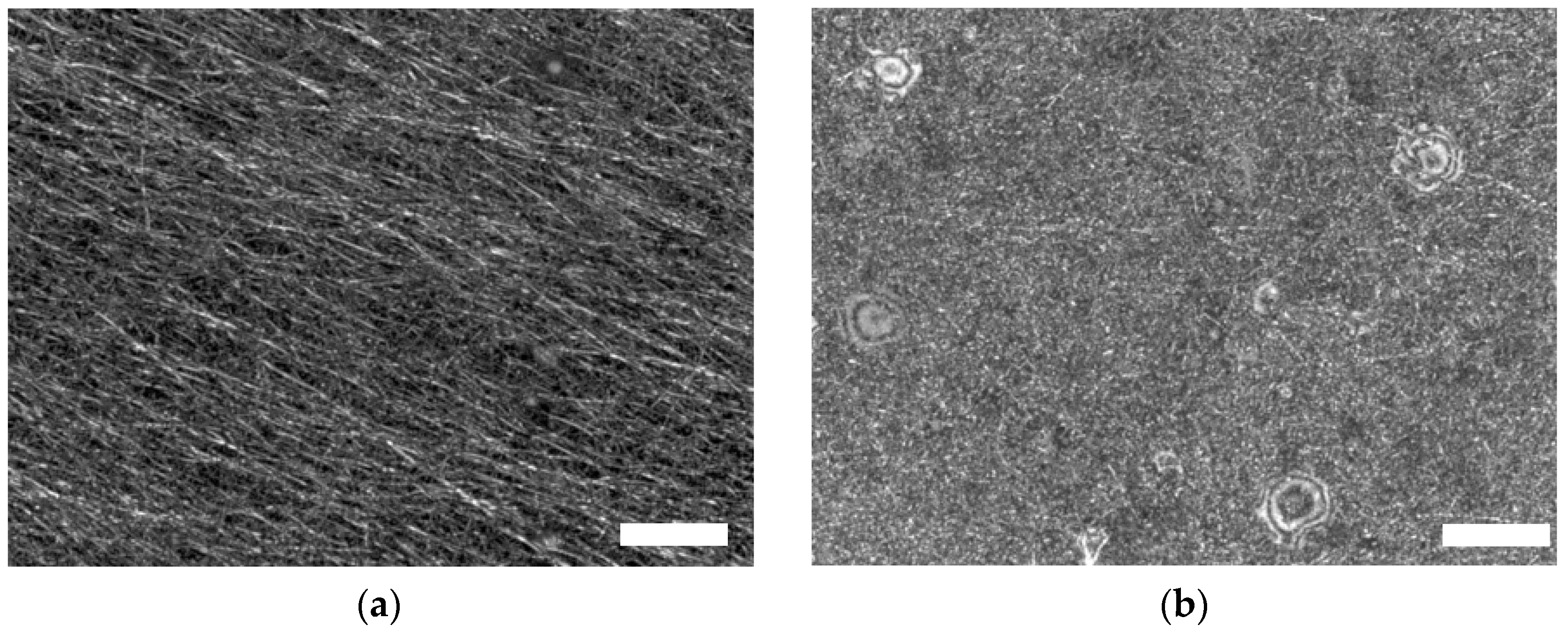
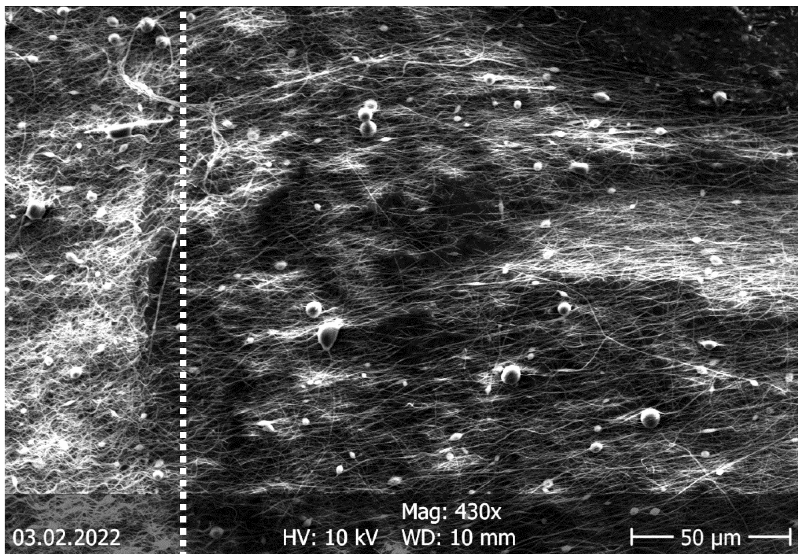
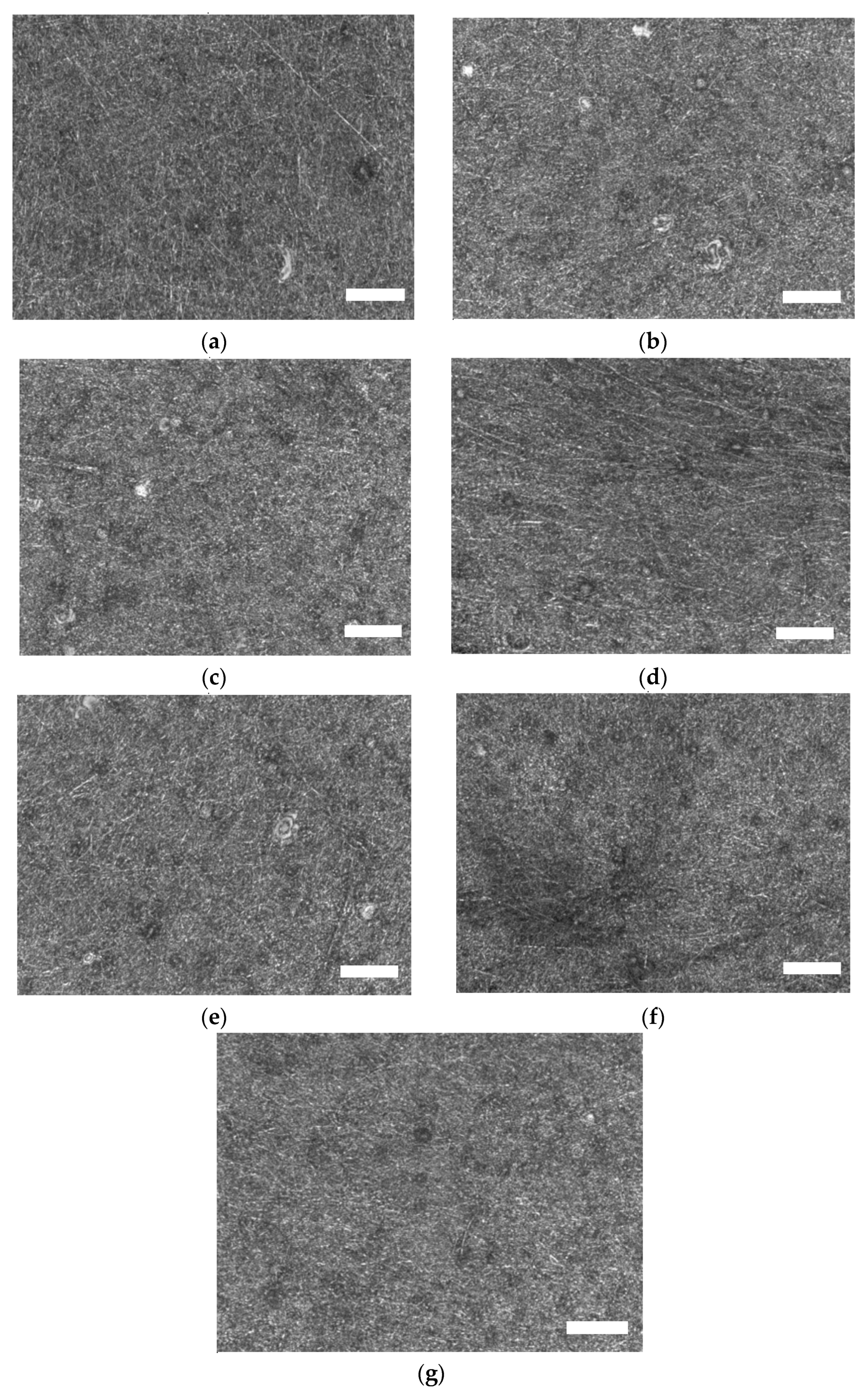
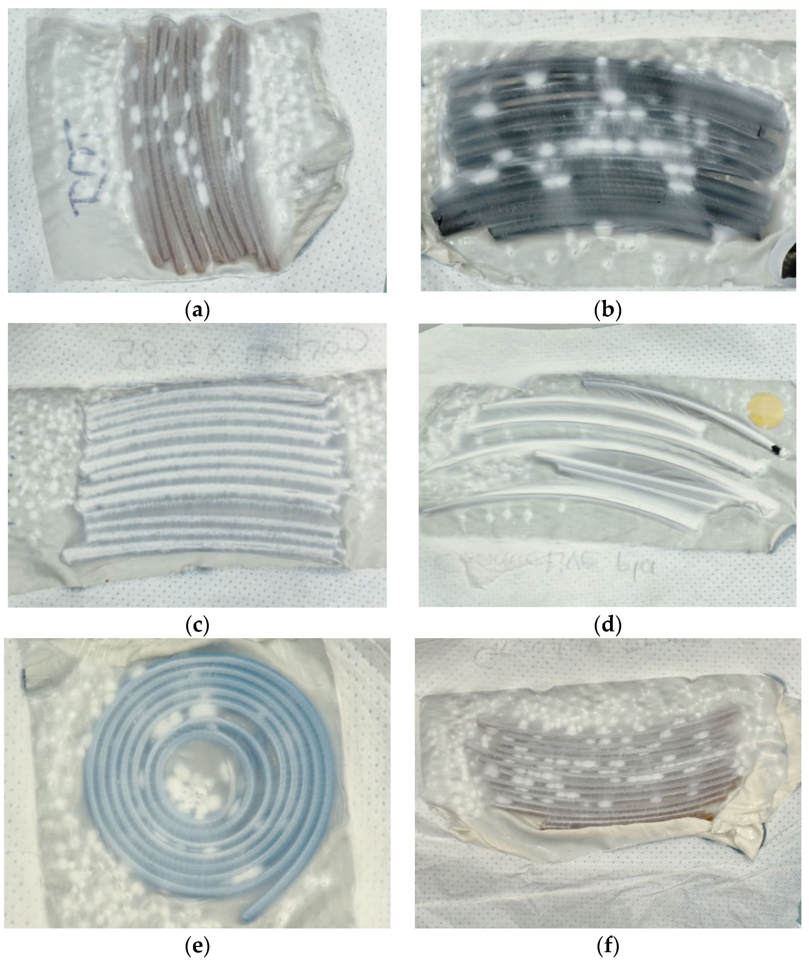
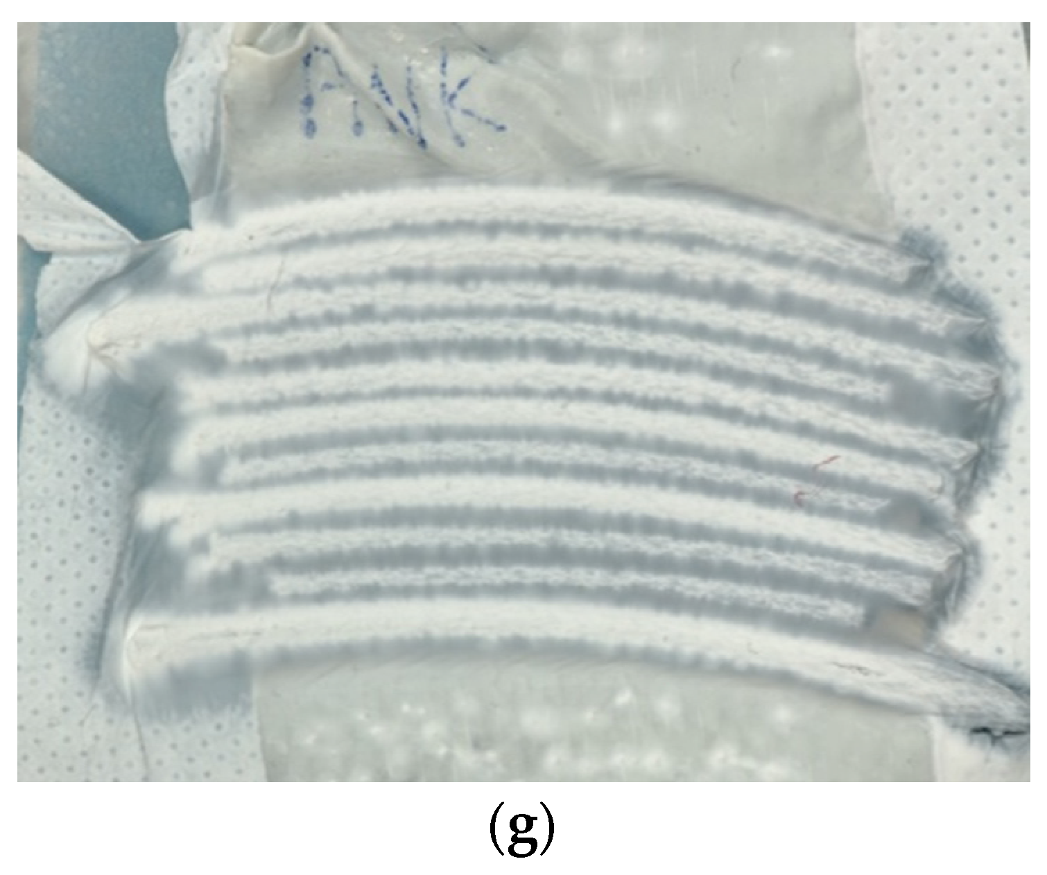
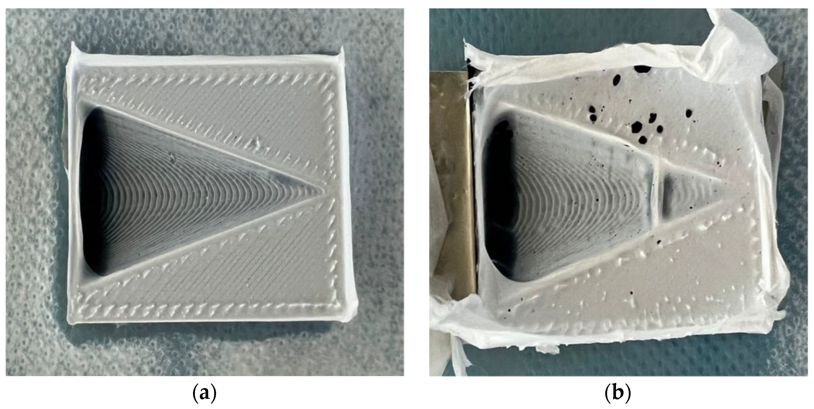
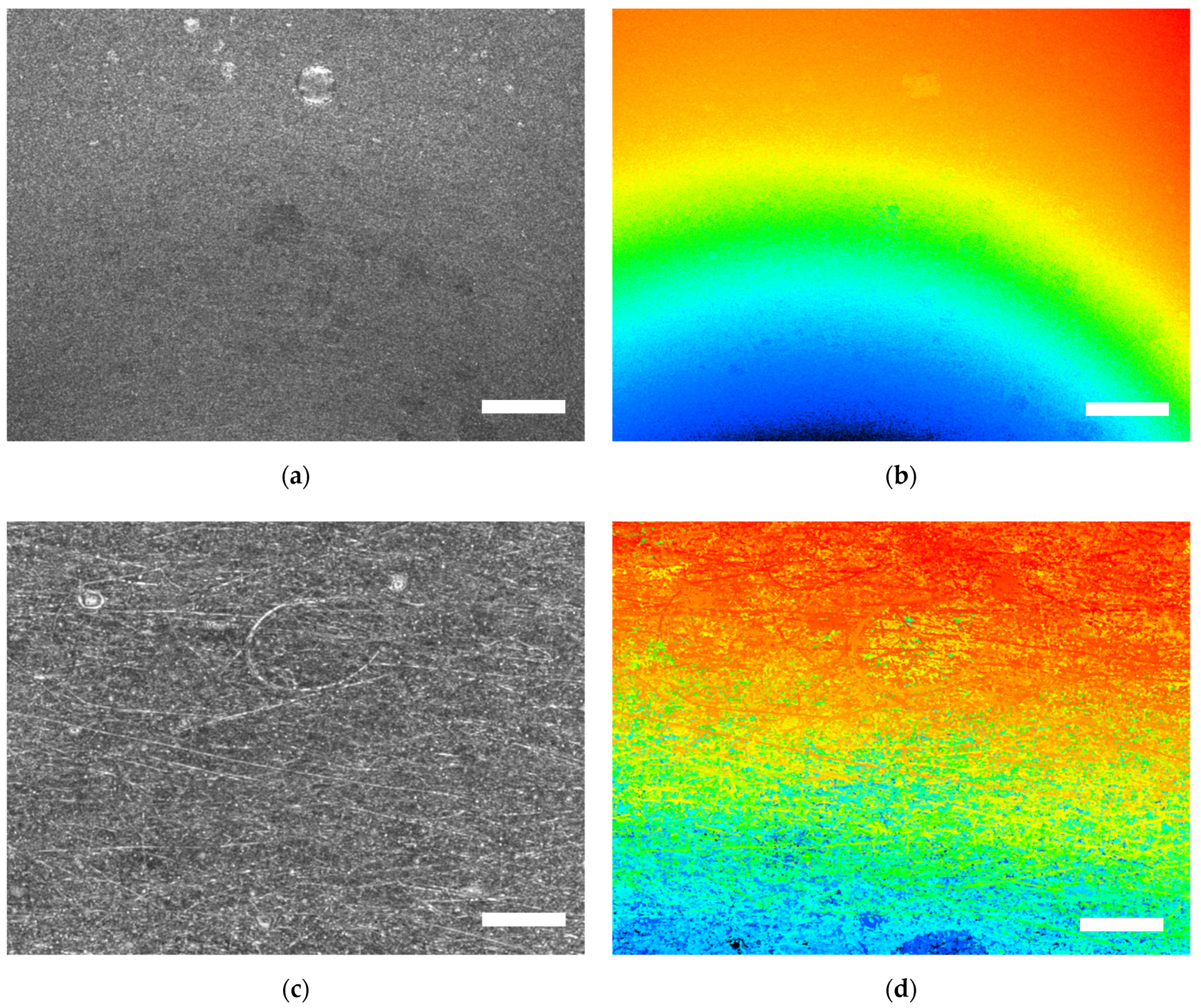
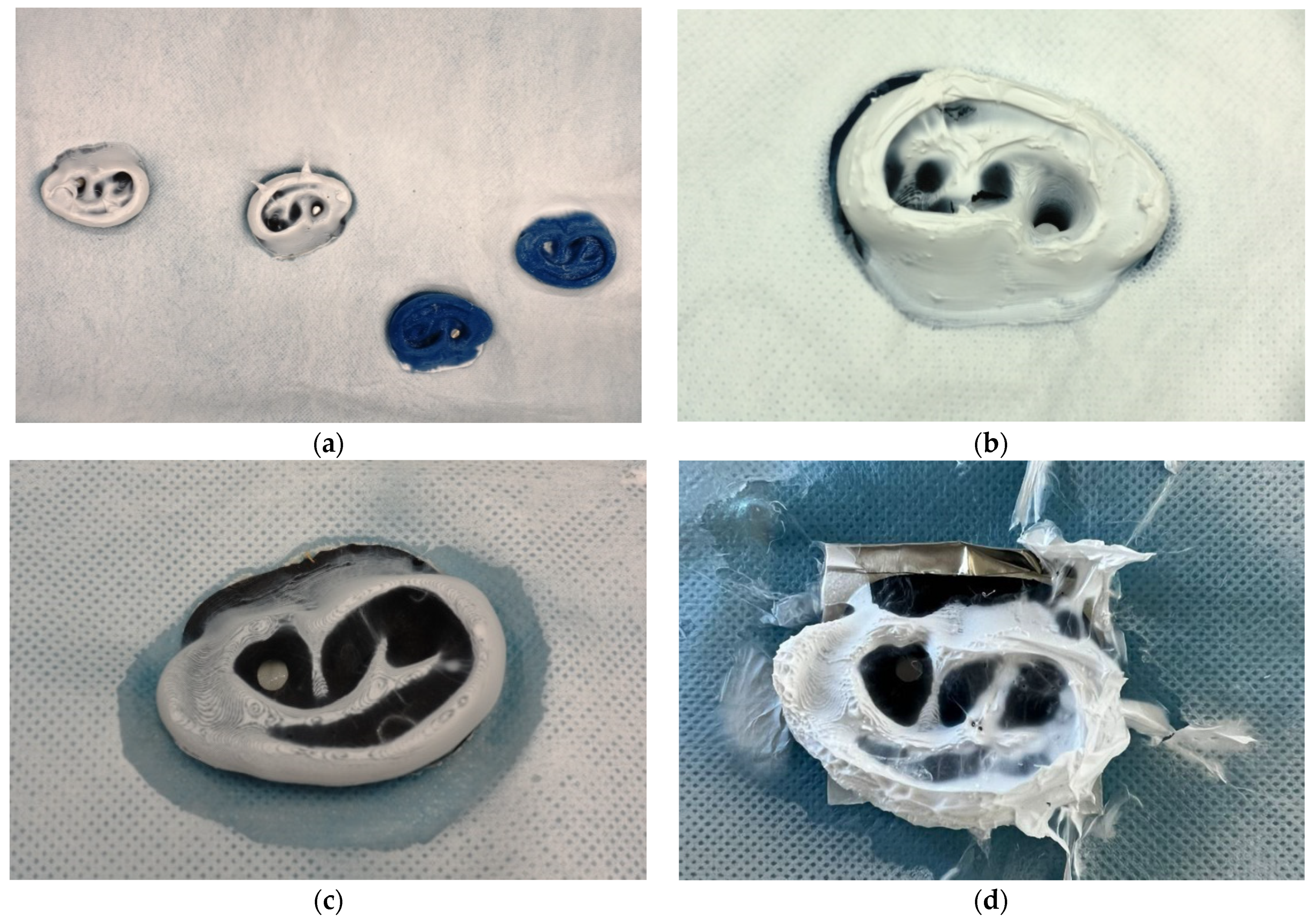
3. Results and Discussion

The first nanofiber mats (V1-V5) were used to investigate the reproducibility of the gained nanofibers mats as well as the influence of additional dextran in the solution, which was shown to result in relatively thick, straight fibers [28]. As expected, the CLSM images showed similar PAN nanofiber mats on an intermediate scale, while sample V4 with a PAN/dextran blend had significantly thicker fibers (Figure 2). Some areas of some of the nanofiber mats contained nonfibrous areas, as visible in Figure 2c. This happens especially in case of slightly increased relative humidity or not-completely exhausted solvent vapor in the chamber after long spinning durations (45 min in case of sample V5).
Another possible difference between nominally identical nanofiber mats is depicted more in Figure 3, using the example of samples V1 and V2. Here, the time dependence of the electrospinning solution was investigated. While the solution for V1 (Figure 3a) was left in the lab for two weeks, the solution used for V2 (Figure 3b) was directly electrospun after stirring for 24 h. It is clearly visible that although no macroscopic differences between the spinning solutions could be recognized, the results differ strongly, with V1 showing relatively thick, straight fibers, while V2 has significantly thinner fibers with beads. These beads typically occur when the spinning solution does not contain a sufficient solid content [29], while thicker fibers are typical for spinning solutions with a higher amount of PAN [30]. This comparison indicates that usual stirring by a magnetic stirrer for some hours does not fully dissolve PAN in DMSO, so that the duration between preparation of the solution and electrospinning should be taken into account as an additional parameter. Here, all other nanofiber mats were electrospun approx. 1–2 days after preparation of the solution.
Next, the influence of nonconductive 3D objects glued on the substrate was tested. Figure 4 depicts a comparison of different areas of sample V6-1, electrospun on (Figure 4a) or next to (Figure 4b) a 3D printed object from PLA with a ratchet-like surface. Interestingly, a clear fiber orientation parallel to the maxima of the ratchet is found on the 3D-printed object, as it was also recognized in an earlier study [12], while no such orientation is visible next to the 3D object (Figure 4b).
Investigating the nanofiber mat on top of the 3D printed object by SEM reveals a similar finding, as visible in Figure 5. The nanofiber mat on top of the object (on the right-hand side of the dotted line) shows a clear fiber orientation, which directly changes when the nanofiber mat is examined on the common polypropylene (PP) nonwoven substrate (left of the dotted line). This underlines the influence of a substrate variation on the nanofiber mat morphology.
To investigate the effect of different materials as substrate modifications further, seven 3D-printing filaments with partly conductive filling (cf. Section 2) were glued on the PP substrate before electrospinning with standard parameters (V9-2) was performed. Figure 6 depicts CLSM images of the surfaces. Most of them look very similar, partly with visible beads or nonfibrous areas (visible as bright, round spots). Only the conductive filament “Conductive PLA” (Figure 6d) shows a clear fiber orientation. It should be mentioned that the optical properties of such PAN nanofiber mats, independent of the fiber orientation, generally show a total transmission around 40–70% (depending on the nanofiber mat thickness) and a specular transmission near 0% throughout the whole visible spectrum without any maxima or minima, corresponding to the typical white color of such nanofiber mats [31,32].
Since CLSM images can only show the fiber near the sample surface and do not allow the depiction of the thickness of the nanofiber mat, the same samples are depicted by macroscopic photographs in Figure 7. Here, it becomes clear that the filaments Carbon X2-85 (Figure 7c), Conductive PLA (Figure 7d) and XT-CF20 (Figure 7g) attract the highest quantity of nanofibers and thus show the thickest nanofiber mats, while the other filaments seem to repel the nanofiber mats. Such an effect has already been recognized in a previous study [12]. The next tests in which nanofiber mats were grown on different 3D-printed shapes were thus performed with Conductive PLA as the most conductive filament, here showing the most regular nanofiber mat on top of it.
Next, 3D-printed funnels were 3D printed to investigate possible shadowing effects at the rounded edges (experiment V12-1, Figure 8). Generally, the surface of both funnels is completely covered with nanofiber mat, with the nanofiber mats following the surface steps of the funnels due to the layer-wise printing, thus causing steps of 0.15 mm height. However, a deeper look at both samples reveals that a thicker nanofiber mat is placed on the funnel with additional copper foil, i.e., a system which modifies the electric field of the electrospinning apparatus more than the pure conductive 3D-printed object. Moreover, nearly no nanofibers are visible on the PP substrate around the conductive print with copper foil below. Comparing both surfaces shows that the nanofiber mat on the pure Conductive PLA object has lower irregularities. The black holes in the nanofiber mat on the funnel on copper foil (Figure 8b) were burnt by small flash-arcs, which can occur in areas with a highly concentrated electric field if the relative humidity is high enough or the spinning solution has a sufficient conductivity.
CLSM images of the apex of the funnel in Figure 8a are depicted in Figure 9 at different magnifications. On both scales, there are no fiber orientations visible, which may be attributed to the small height gradient inside the funnel. The height plot in Figure 9b shows two of the steps due to the printing process (from the orange plateau to the green layer below and the blue layer below the green one). These steps are no longer visible at higher magnification (Figure 9d).
As a stronger 3D-shaped object, 3D-printed ears were tested as substrates (V10, V11 and V12-2). Tests were performed comparing PLA and Conductive PLA as printing materials; the ears were partly placed on additional conductive copper foils, and they were partly additionally grounded. PAN/dextran and pure PAN nanofiber mats were electrospun on them. Figure 10 depicts some of the results of these tests.
As already expected, the pure PLA ears strongly repelled the nanofibers, while ears printed from Conductive PLA showed a nanofiber mat similar to the surrounding PP nonwoven (Figure 10a). No macroscopic differences are visible comparing PAN/dextran (Figure 10b) and PAN nanofiber mats. The inner areas of the ear, however, are not covered by nanofibers in these tests.
This is why subsequent tests were performed with reduced voltage to examine the influence of this parameter on the covering of the 3D-printed objects (Figure 10c,d). However, the shadowing effect became even stronger, as compared to Figure 10a,b. This can be explained by the nanofibers impinging on the substrate at a smaller speed if the voltage is lower, in this way being stronger directed towards the highest conductive areas and thus leaving more lower areas inside the ear uncovered. Furthermore, the influence of an additional highly conductive copper foil below the ear from Conductive PLA (Figure 10d) is clearly visible, as it was already recognized in Figure 8. Apparently, Conductive PLA has a well-suitable conductivity to avoid repelling a nanofiber mat without deforming the electric field so strongly that highly irregular nanofiber mats are formed, as visible in Figure 9d. This shows that material and shape have to be tailored carefully to enable the covering of the whole surface, possibly even by combining different 3D-printing polymers in one object, which is possible with several recent 3D printers.
In order to prepare 3D substrates for tissue engineering with a nanostructured surface, it is nevertheless necessary to enable coating the whole surface by a nanofiber mat. One possible approach to reach this aim is by using so-called 4D printing, i.e., 3D-printing a plane object that can be deformed afterwards by heat or other stimuli [33]. Since PLA belongs to the so-called shape-memory polymers, which enable 4D printing [34], the shape-memory properties of the Conductive PLA under investigation in the recent study will be investigated in a future study.

4. Conclusions

Electrospinning PAN and PAN/dextran nanofiber mats was performed on diverse 3D-printing polymers. Depending on their shape, thickness and conductivity, the nanofibers were repelled or strongly attracted. 3D-printed ears from conductive PLA were covered along the higher parts, while varying spinning and solution parameters did not enable covering the whole surface of the structure. Oppositely, 3D-printed funnels with lower slope could be completely covered, with the electrospun nanofiber mat following the surface structure given by the 3D-printing process. Along the borders of some 3D-printed materials, a clear fiber orientation was found, which can be used for oriented cell growth.
As a possible solution, 4D-printing of conductive shape-memory polymers will be investigated in a future study. Moreover, biocompatibility in general, as well as mammalian cell adhesion and proliferation, will be tested for different conductive PLA materials. Finally, degradation of PLA in cell-culture medium has to be evaluated, especially related to the potential influence of the nanofiber mat grown on it.

Author Contributions

Conceptualization, T.G.; methodology, T.G. and A.E.; validation, T.G. and A.E.; formal analysis, T.G. and A.E.; investigation, all authors; writing—original draft preparation, T.G. and A.E.; writing—review and editing, all authors.; visualization, U.G., T.G. and A.E. All authors have read and agreed to the published version of the manuscript.

Funding

This research was partly funded by the German Federal Ministry for Economic Affairs and Energy as part of the Central Innovation Program for SMEs (ZIM) via the AiF, based on a resolution of the German Bundestag, grant number KK5129703CR0.

Institutional Review Board Statement

Not applicable.

Informed Consent Statement

Not applicable.

Data Availability Statement

All data are shown in this paper.

Conflicts of Interest

The authors declare no conflict of interest. The funders had no role in the design of the study; in the collection, analyses, or interpretation of data; in the writing of the manuscript; or in the decision to publish the results.

References

  1. Arkoun, M.; Daigle, F.; Heuzey, M.-C.; Ajji, A. Antibacterial electrospun chitosan-based nanofibers: A bacterial membrane perforator. Food Sci. Nutr. 2017, 5, 865–874. [Google Scholar] [CrossRef] [PubMed]
  2. Yalcinkaya, F. A review on advanced nanofiber technology for membrane distillation. J. Eng. Fibers Fabr. 2019, 14, 1558925018824901. [Google Scholar] [CrossRef]
  3. Agarwal, S.; Wendorff, J.H.; Greiner, A. Use of electrospinning technique for biomedical applications. Polymer 2008, 49, 5603–5621. [Google Scholar] [CrossRef] [Green Version]
  4. Cengiz, F.; Krucinska, I.; Gliscinska, E.; Chrzanowski, M.; Göktepe, F. Comparative analysis of various electrospinning methods of nanofibre formation. Fibres Text. East. Eur. 2009, 72, 13–19. [Google Scholar]
  5. Bhardwaj, N.; Kundu, S.C. Electrospinning: A fascinating fiber fabrication technique. Biotechnol. Adv. 2010, 28, 325–347. [Google Scholar] [CrossRef]
  6. Greiner, A.; Wendorff, J.H. Electrospinning: A fascinating method for the preparation of ultrathin fibers. Angew. Chem. Int. Ed. 2007, 46, 5670–5703. [Google Scholar] [CrossRef]
  7. Li, D.; Xia, Y. Electrospinning of nanofibers: Reinventing the wheel? Adv. Mater. 2004, 16, 1151–1170. [Google Scholar] [CrossRef]
  8. Bertocchi, M.J.; Simbana, R.A.; Wynne, L.H.; Lundin, J.G. Electrospinning of tough and elastic liquid crystalline polymer-polyurethane composite fibers: Mechanical properties and fiber alignment. Macromol. Mater. Eng. 2019, 304, 1900186. [Google Scholar] [CrossRef]
  9. Bazrafshan, Z.; Stylios, G.K. A novel approach to enhance the spinnability of collagen fibers by graft polymerization. Mater. Sci. Eng. 2019, 94, 108–116. [Google Scholar] [CrossRef]
  10. Storck, J.L.; Grothe, T.; Mamun, A.; Sabantina, L.; Klöcker, M.; Blachowicz, T.; Ehrmann, A. Orientation of electrospun magnetic nanofibers near conductive areas. Materials 2020, 13, 47. [Google Scholar] [CrossRef] [Green Version]
  11. Nguyen, D.N.; Hwang, Y.; Moon, W. Electrospinning of well-aligned fiber bundles using an end-point control assembly method. Eur. Polym. J. 2016, 77, 54–64. [Google Scholar] [CrossRef]
  12. Hellert, C.; Storck, J.L.; Grothe, T.; Kaltschmidt, B.; Hütten, A.; Ehrmann, A. Positioning and aligning electrospun PAN fibers by conductive and dielectric substrate patterns. Macromol. Symp. 2021, 395, 2000213. [Google Scholar] [CrossRef]
  13. Guarino, V.; Iannotti, V.; Ausanio, G.; Ambrosio, L.; Lanotte, L. Elastomagnetic nanofiber wires by magnetic field assisted electrospinning. Express Polym. Lett. 2019, 13, 419–428. [Google Scholar] [CrossRef]
  14. Johnson, C.D.L.; Ganguly, D.; Zuidema, J.M.; Cardina, T.J.; Ziemba, A.M.; Kearns, K.R.; McCarthy, S.M.; Thompson, D.M.; Ramanath, G.; Borca-Tasciuc, D.A.; et al. Injectable, magnetically orienting electrospun fiber conduits for neuron guidance. ACS Appl. Mater. Interfaces 2019, 11, 356–372. [Google Scholar] [CrossRef] [PubMed]
  15. Cooper, A.; Oldinski, R.; Ma, H.; Bryers, J.D.; Zhang, M. Chitosan-based nanofibrous membranes for antibacterial filter applications. Carbohydr. Polym. 2013, 92, 254–259. [Google Scholar] [CrossRef] [Green Version]
  16. Ehrmann, A. Non-toxic crosslinking of electrospun gelatin nanofibers for tissue engineering and biomedicine—A review. Polymers 2021, 13, 1973. [Google Scholar] [CrossRef]
  17. Nam, J.; Huang, Y.; Agarwal, S.; Lannutti, J. Materials selection and residual solvent retention in biodegradable electrospun fibers. J. Appl. Polym. Sci. 2008, 107, 1547–1554. [Google Scholar] [CrossRef]
  18. Fatih Canbolat, M.; Tang, C.; Bernacki, S.H.; Pourdeyhimi, B.; Khan, S. Mammalian cell viability in electrospun composite nanofiber structures. Macromol. Biosci. 2011, 11, 1346–1356. [Google Scholar] [CrossRef]
  19. Wortmann, M.; Frese, N.; Sabantina, L.; Petkau, R.; Kinzel, F.; Gölzhäuser, A.; Ehrmann, A. New polymers for needleless electrospinning from low-toxic solvents. Nanomaterials 2019, 9, 52. [Google Scholar] [CrossRef] [Green Version]
  20. Plamus, T.; Savest, N.; Viirsalu, M.; Harz, P.; Tarasova, E.; Krasnou, I.; Krumme, A. The effect of ionic liquids on the mechanical properties of electrospun polyacrylonitrile membranes. Polym. Test. 2018, 71, 335–343. [Google Scholar] [CrossRef]
  21. Krasonu, I.; Tarassova, E.; Malmberg, S.; Vassiljeva, V.; Krumme, A. Preparation of fibrous electrospun membranes with activated carbon filler. IOP Conf. Ser. Mater. Sci. Eng. 2019, 500, 012022. [Google Scholar] [CrossRef]
  22. Wehlage, D.; Blattner, H.; Mamun, A.; Kutzli, I.; Diestelhorst, E.; Rattenholl, A.; Gudermann, F.; Lütkemeyer, D.; Ehrmann, A. Cell growth on electrospun nanofiber mats from polyacrylonitrile (PAN) blends. AIMS Bioeng. 2020, 7, 43–54. [Google Scholar] [CrossRef]
  23. Wehlage, D.; Blattner, H.; Sabantina, L.; Böttjer, R.; Grothe, T.; Rattenholl, A.; Gudermann, F.; Lütkemeyer, D.; Ehrmann, A. Sterilization of PAN/gelatin nanofibrous mats for cell growth. Tekstilec 2019, 62, 78–88. [Google Scholar] [CrossRef]
  24. Yu, Y.X.; Hua, S.; Yang, M.K.; Fu, Z.Z.; Teng, S.S.; Niu, K.; Zhao, Q.H.; Yi, C.Q. Fabrication and characterization of electrospinning/3D printing bone tissue engineering scaffold. RSC Adv. 2016, 6, 110557–110565. [Google Scholar] [CrossRef]
  25. Muerza-Cascante, M.L.; Shokoohmand, A.; Khosrotehrani, K.; Haylock, D.; Dalton, P.D.; Hutmacher, D.W.; Loessner, D. Endosteal-like extracellular matrix expression on melt electrospun written scaffolds. Acta Biomater. 2017, 52, 145–158. [Google Scholar] [CrossRef] [Green Version]
  26. De Mori, A.; Pena Fernández, M.; Blunn, G.; Tozzi, G.; Roldo, M. 3D Printing and Electrospinning of Composite Hydrogels for Cartilage and Bone Tissue Engineering. Polymers 2018, 10, 285. [Google Scholar] [CrossRef] [Green Version]
  27. Trabelsi, M.; Mamun, A.; Klöcker, M.; Sabantina, L.; Großerhode, C.; Blachowicz, T.; Ehrmann, A. Increased mechanical properties of carbon nanofiber mats for possible medical applications. Fibers 2019, 7, 98. [Google Scholar] [CrossRef] [Green Version]
  28. Böttjer, R.; Grothe, T.; Wehlage, D.; Ehrmann, A. Electrospraying poloxamer/(bio-) polymer blends using a needleless electrospinning machine. J. Text. Fibrous Mater. 2018, 1, 2515221117743079. [Google Scholar] [CrossRef]
  29. Sabantina, L.; Rodríguez Mirasol, J.; Cordero, T.; Finsterbusch, K.; Ehrmann, A. Investigation of needleless electrospun PAN nanofiber mats. AIP Conf. Proc. 2018, 1952, 020085. [Google Scholar]
  30. Grothe, T.; Storck, J.L.; Dotter, M.; Ehrmann, A. Impact of solid content in the electrospinning solution on the physical and chemical properties of polyacrylonitrile (PAN) nanofibrous mats. Tekstilec 2020, 63, 225–232. [Google Scholar] [CrossRef]
  31. Kerker, E.; Steinhäußer, D.; Mamun, A.; Trabelsi, M.; Fiedler, J.; Sabantina, L.; Juhász Junger, I.; Schiek, M.; Ehrmann, A.; Kaschuba, R. Spectroscopic investigation of highly-scattering nanofiber mats during drying and film formation. Optik 2020, 208, 164081. [Google Scholar] [CrossRef]
  32. Grothe, T.; Böhm, T.; Habashy, K.; Abdullaeva, O.S.; Zablocki, J.; Lützen, A.; Dedek, K.; Schiek, M.; Ehrmann, A. Optical Index Matching, Flexible Electrospun Substrates for Seamless Organic Photocapacitive Sensors. Phys. Status Solidi B 2021, 258, 2000543. [Google Scholar] [CrossRef]
  33. Koch, H.C.; Schmelzeisen, D.; Gries, T. 4D textiles made by additive manufacturing on pre-stressed textiles—An overview. Actuators 2021, 10, 31. [Google Scholar] [CrossRef]
  34. Ehrmann, G.; Ehrmann, A. 3D printing of shape memory polymers. J. Appl. Polym. Sci. 2021, 138, 50847. [Google Scholar] [CrossRef]
Figure 1. Sketch of the nanofiber setup: The high-voltage electrode wire (black) is coated by the polymer solution (green). The latter is dragged by the strong electric field towards the ground electrode, before which it is deposited on a substrate (blue) or on objects glued onto the substrate (grey).
Technologies 10 00066 g001
Figure 2. CLSM images of nanofiber mats: (a) V3 containing pure PAN; (b) V4 containing a PAN/dextran blend; (c) V5 containing pure PAN. Scale bars indicate 20 µm.
Technologies 10 00066 g002
Figure 3. SEM images of (a) sample V1; (b) sample V2. Scale bars indicate 7 µm.
Technologies 10 00066 g003
Figure 4. CLSM images of sample V6-1 (a) on a 3D-printed object; (b) next to a 3D-printed object. Scale bars indicate 20 µm.
Technologies 10 00066 g004
Figure 5. SEM image of sample V6-1 next to the border (approximated by the dotted line) of the 3D-printed object.
Technologies 10 00066 g005
Figure 6. CLSM images of PAN nanofiber mats on 3D-printing filaments: (a) Bronzefill; (b) CarbonFil; (c) Carbon X2-85; (d) Conductive PLA; (e) Filaflex; (f) Growlay; (g) XT-CF20. Scale bars indicate 20 µm.
Technologies 10 00066 g006
Figure 7. Photographic images of PAN nanofiber mats on 3D-printing filaments: (a) Bronzefill; (b) CarbonFil; (c) Carbon X2-85; (d) Conductive PLA; (e) Filaflex; (f) Growlay; (g) XT-CF20. All filament diameters are 1.75 mm.
Technologies 10 00066 g007aTechnologies 10 00066 g007b
Figure 8. PAN electrospun on funnels printed with Conductive PLA: (a) glued on the PP substrate; (b) glued on a copper foil on the PP substrate. The funnels have a length of 40 mm and width of 31 mm.
Technologies 10 00066 g008
Figure 9. CLSM images of the apex of the funnel in Figure 8a: (a) morphology with 200× magnification; (b) height plot with 200× magnification; (c) morphology with 2000× magnification; (d) height plot with 2000× magnification. Scale bars correspond to 200 µm (a,b) and 20 µm (c,d), respectively.
Technologies 10 00066 g009
Figure 10. 3D-printed ears decorated with electrospun nanofiber mats: (a) from left to right: PAN on Conductive PLA on copper foil, Conductive PLA on aluminum foil, PLA on copper foil, PLA on PP substrate (V11); (b) PAN/dextran on Conductive PLA; (c) PAN on Conductive PLA (50 kV); (d) PAN on Conductive PLA on copper foil (50 kV). All ears have a length of 59 mm (longest side).
Technologies 10 00066 g010
Table 1. Assignment of the sample description, the associated 3D printed parts and its spinning parameters. Due to the overview, only the altered parameters are shown.
Description3D Printed PartSpinning SolutionVoltageCurrentDuration
V1 None16% PAN80 kV0.116 mA30 min
V2None16% PAN80 kV0.08 mA30 min
V3None16% PAN80 kV0.08 mA30 min
V4None16% PAN + 5% dextran80 kV0.04 mA31 min
V5None14% PAN80 kV0.04 mA45 min
V6Various 3D parts14% PAN81 kV0.032 mA30 min
V6-1Various 3D parts14% PAN81 kV0.032 mA30 min
V6-2Various 3D parts14% PAN81 kV0.032 mA30 min
V7Aluminum foil14% PAN81 kV0.032 mA30 min
V9-23D filaments14% PAN80 kV0.03 mA30 min
V103D printed ear12% PAN + 2% dextran80 kV0.03 mA17 min
V113D printed ears from different filaments13% PAN80 kV0.03 mA25 min
V12-13D printed funnel in profile13% PAN82 kV0.03 mA16 min
V12-23D printed ears
(partly grounded)
13% PAN50 kV0.016 mA30 min
Publisher’s Note: MDPI stays neutral with regard to jurisdictional claims in published maps and institutional affiliations.

