
Maxwell–Wagner Effect in Multi-Layered Dielectrics: Interfacial Charge Measurement and Modelling


1
Electrical Engineering Department, Electric Power University, 235 Hoang Quoc Viet, Hanoi 10000, Vietnam
2
Laboratory on Plasma and Conversion of Energy (LAPLACE), Université de Toulouse, CNRS, INPT, UPS, Bat 3R3, 118, route de Narbonne, 31062 Toulouse, France
*
Author to whom correspondence should be addressed.
Technologies 2017, 5(2), 27; https://0-doi-org.brum.beds.ac.uk/10.3390/technologies5020027
Submission received: 11 April 2017
/
Revised: 12 May 2017
/
Accepted: 25 May 2017
/
Published: 29 May 2017
(This article belongs to the Section Innovations in Materials Processing)
Abstract
:The development of high voltage direct current (HVDC) technologies generates new paradigms in research. In particular and contrary to the AC case, investigation of electrical conduction is not only needed for understanding the dielectric breakdown but also to describe the field distribution inside the insulation. Here, we revisit the so-called Maxwell–Wagner effect in multi-layered dielectrics by considering on the one hand a non-linear field dependent model of conductivity and on the other hand by performing space charge measurements giving access to the interfacial charge accumulated between different dielectrics. We show that space charge measurements give access to the amount of interfacial charge built-up by the Maxwell–Wagner effect between two dielectrics of different natures. Measurements also demonstrate that the field distribution undergoes a transition from a capacitive distribution to a resistive one, under long lasting stress.
1. Introduction
The development of high voltage links for energy transport under DC voltage (HVDC) is boosted by the new generation of converters and, at the same time, by the need to interconnect networks allowing reliable delivery of electric energy from regions of production to regions of consumption. These technologies bring about new paradigms associated with the design and the behavior under the stress of electrical insulation. As opposed to the AC case where field distribution is essentially capacitive and described by the value of the permittivity of the materials, it is resistive in the DC case. If the permittivity is weakly sensitive to the field or temperature in such a way that the AC field distribution is rather well controlled, it is opposed for the resistivity that drastically depends on temperature and is highly non-linear in field for the targeted working stresses.
In DC power cables, the consequence is that the field distribution cannot be derived from the AC case [1,2]. This is a due to the field divergence in a cylindrical geometry together with the non-linearity of the resistivity but also of the thermal gradient that exists between the cable core and the outer screen. The current flow in the core generates a source of heat due to the Joule effect. Cables with extruded synthetic insulation (cross-linked polyethylene—XLPE) used for years under AC, tend to replace the old but reliable technology of oil-filled cable for DC transport, mainly for easy maintenance and environmental reasons [3]. The trend nowadays is towards XLPE insulated cables with a service temperature of 90 °C at the core and a design field of 20 kV/mm, if not more. The service voltage for cross-linked insulation is for example 320 kV for the HVDC France-Spain link [4], and projects towards 500 kV are under study [5,6].
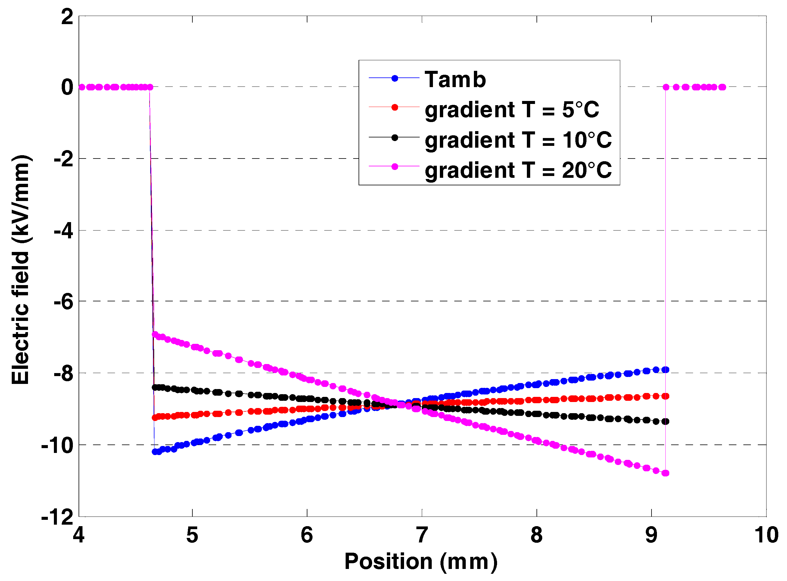
Figure 1 shows an example of field distribution in the insulation of a medium voltage–MV cable in a stationary regime under different thermal conditions. The results correspond to a model using a field dependent conductivity of the same kind as the one used in the present study [7]. Under a thermal gradient, an inversion of the electrical stress occurs: the position of the maximum stress moves from the inner radius of the insulation to the outer part of the cable. In a real situation, the stationary regime is never strictly achieved vs. field and temperature. Besides, space charge phenomena appear which are not linked with the apparent conductivity in such a way that the real field distribution is difficult to predict. Two risks arise as consequences: the field can exceed locally the design field and it is strengthened at the outer part of the cable. The outer part of the insulation is a critical place to manage the field for accessories such as joints and terminations and these are weak points of the whole energy transmission system.
The contact between dielectrics of different natures, in particular in accessories, coupled to non-linear effects, renders the field distribution tricky to evaluate in service [8,9]. To alleviate this issue, specific measurement techniques can be implemented for field distribution estimation through space charge density distribution, which are pertinent for insulation design [10]. In this work, we present an investigation on interfacial charge between two dielectrics of different nature. The interfacial charge, which is derived from Maxwell’s equations, is computed in a non-linear regime in field from the experimental data on conductivity vs. field and temperature. Space charge measurements are implemented and compared to the model prediction. The work is in-line with previous achievements by Bodega [11,12] who considered the association of XLPE and EPR (ethylene-propylene rubber) either in thick-plaque samples or in miniature cables, pushing the analysis to the coaxial structure with bilayer insulation and considering the response under the thermal gradient. Because of the specific properties of the investigated material, conductivity is always higher in the EPR layer, meaning that the electric stress is higher in the XLPE. In the present work, we address a case where the sign of the interface charge is changing according to the chosen combination of electrical and thermal stresses. The decay kinetics of the charge is analyzed, still in the frame of the Maxwell–Wagner model. Such analysis of the charge decay was not proposed in earlier works on interface charge measurements. We evaluate here how long-lasting the previously stored charge in a DC system under short circuit conditions can be.
2. Materials and Methods
2.1. Material Properties
The investigated system is shown in Figure 2. It consists of a bilayer structure made of a chemically (peroxide) crosslinked polyethylene and a material used for reconstructing the insulation of the cable when joining two cable sections (an elastomer ethylene-propylene-diene monomer—EPDM). The dielectric permittivity of XLPE and EPDM are considered field and temperature independent. Indeed, variations in permittivity do not exceed 10% in the temperature range from 20 to 100 °C [13]. The relative values used in the study are ε1r = 2.3; ε2r = 2.9. Sandwich structures were processed in two steps: First, samples of each of the components were press-molded at 120 °C for 5 min into disks of 80 mm in diameter. In a second step, the disks were assembled and crosslinked altogether at 180 °C for 15 min still by press-molding. The expected thicknesses of the structure were d1 = d2 = 250 to 300 µm. However, as the two materials have different viscosities, it was not easy to perfectly control the layer thicknesses—the latter were deduced a posteriori. In the example of space charge results shown below, the thicknesses were 200 and 350 µm. Results with more equilibrated structures are reported in [14]. The general trends for the field distribution are the same.
The input data used in the modelling approach are issued from conductivity measurements realized in a previous work [14]. For each of the materials, the conductivity was estimated after 1 h charging time as a function of temperature (20 to 90 °C) and field (2 to 30 kV/mm), on 500 µm-thick films metallized with gold electrodes of 20 cm² area. These experimental data were fitted to a law of the type:
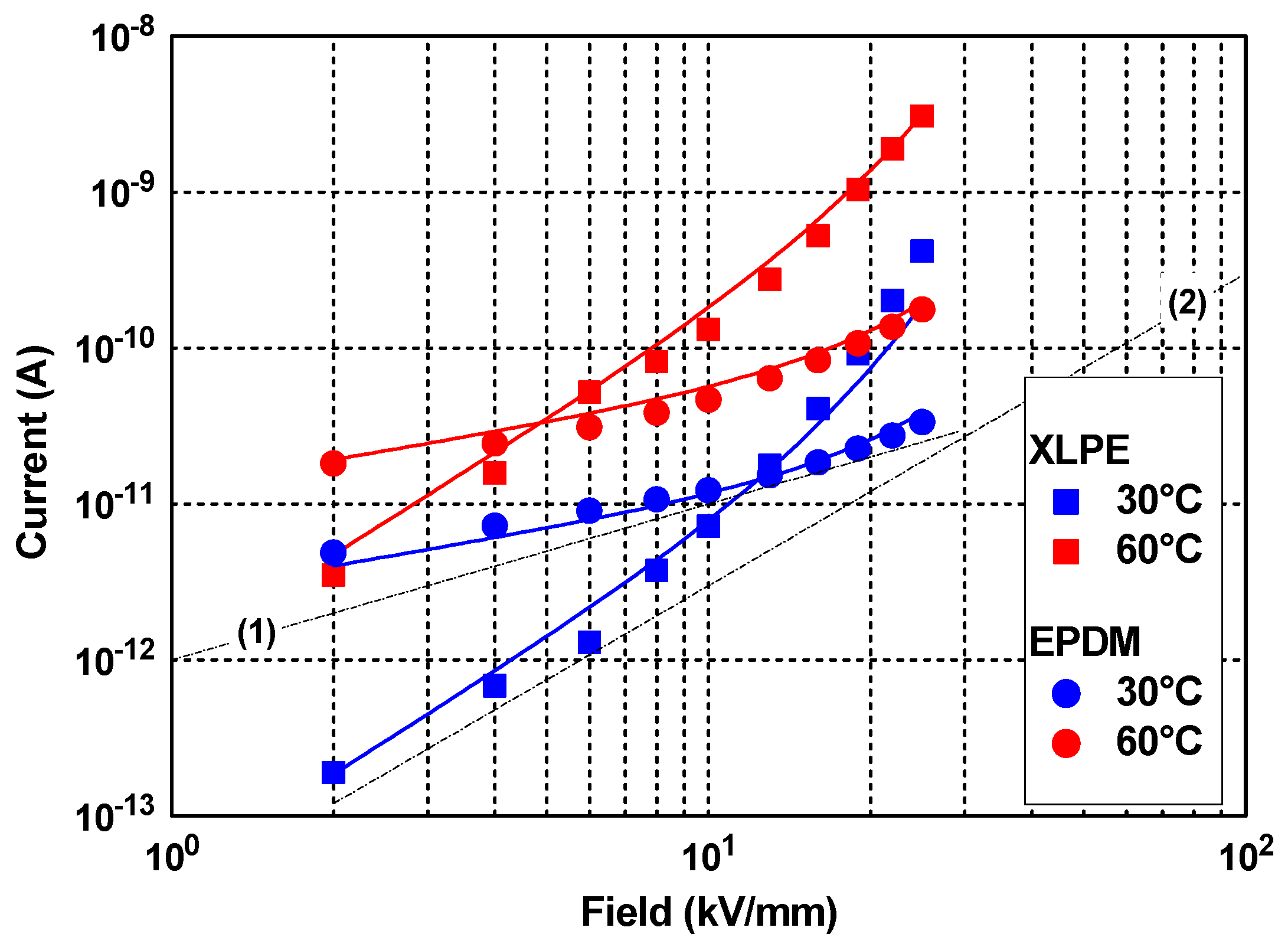
where E is the field, T is the temperature, kB is the Boltzmann’s constant (8.62 × 10⁻⁵ eV/K), and the other symbols are coefficients with values reported in Table 1. Figure 3 shows the current-voltage characteristics for different temperatures: one notes a sub-linear variation in the case of EPDM at low fields, which means that the conductivity decreases with the applied field. A possible explanation of this sub-linear trend can be given by considering ionic conduction as observed in liquid dielectrics [15]: the amorphous polymer EPDM can be considered as a liquid of high viscosity in the temperature range used in this study [14].
2.2. Modelling of the Field Distribution
From the Maxwell–Wagner theory, the field distribution in a stationary regime derives from the following set of equations:
where is the permittivity, is the conductivity, and is the interfacial charge. From Figure 3, the conductivity is at a maximum in one or the other material, depending on the field value. The crossover field depends on the temperature (for example, here it is 12 kV/mm at 30 °C and 5 kV/mm at 60 °C). In these conditions, the interfacial charge is either positive or negative, with the convention of orientation given in Figure 2. The equations describing the non-stationary regime are the same and they are obtained by incorporating the time dependence of the fields E1 and E2 and writing the interfacial charge density in the form [16]:
with:
As the fields E1 and E2 vary in time during the redistribution of the interface charge, the conductivities and depend also on the time due to the non-linear behavior.
Our purpose in the work is to compute the interfacial charge derived from the experimental conductivity values and subsequently to compare it to experimental measurements of the space charge. The first step is therefore to compute the charge in polarization and depolarization in a transient regime.
Equations (5) and (6) cannot be resolved analytically taking into account the field non-linearity: the time constant τMW varies with the field redistribution in the insulation bulk. Therefore, we used a numerical resolution by FEM (finite elements method) using Comsol software. At the initial stage, one considers a purely capacitive field distribution hypothesizing a charge-free system. Therefore:
The numerical resolution is achieved in 1D in time combining Equations (2)–(4) with the initial condition as in (7). The outputs are field values E1(t) and E2(t) and interface charge (t).
2.3. Space Charge Measurements
In principle, different space charge measurement methods can be applied to probe multilayer dielectrics. Three main families exist based on the perturbation of the charge state: thermal methods, based on the propagation of a thermal perturbation producing influence charge variation on the electrode and therefore an external electrical response, pressure wave propagation (PWP) method, with perturbation as an acoustic wave producing a displacement of the internal charges, and the pulsed electroacoustic (PEA) method based on the displacement of the charges through a field pulse, the detected response being an acoustic wave. The application of such methods has been reviewed recently [17]. For application to multi-dielectrics, acoustic methods are a priori preferable as the diffusive nature of heat propagation alters the spatial resolution far from the heat source, i.e., in the middle of the samples. Case studies for inhomogeneous dielectrics are treated for the various techniques by Holé et al. [18]. So far, most of the works on space charge measurements in multi-dielectrics have been achieved by the PEA method [10,14,19]. The application of acoustic methods to recover the charge distribution requires the treatment of acoustic wave propagation and transmission into the various layers. A thorough analysis of the problem for the PEA method has been achieved by Bodega et al. [10]; such an analysis has been reconsidered recently [20].
In the present work, space charge measurements were realized using a PEA set-up provided by TechImp, Italy. The test set-up was installed in a thermostated oven. Space charge measurements were achieved in the temperature range from 20 to 70 °C. Gold electrodes of 20 mm diameter were deposited by sputtering onto both faces of the samples. Voltage pulses of 10 ns duration, and 600 V amplitude were applied at a 2 kHz frequency. The stress cycle consisted of 1 h or 3 h charging time and 1 h discharging time. The charging time was limited for favoring the acquisition of data for several field values in a reasonable experimental time. The field steps in the range from 2 to 30 kV/mm were applied consecutively on the same sample. One new sample was used at each measurement temperature. For the charge distribution recovery, different factors have to be addressed specifically in the case of multi-dielectrics, related to the change in sound velocity from one sample to the other, the change in acoustic impedance with possible reflection effects, and the calibration step related to the change in permittivity. Here, the deconvolution procedure accounts for the permittivity variation as well as the change in sound velocity in the two materials [14] since they are different: 1800 vs. 2100 m/s, for EPDM and XLPE, respectively. The reflection of acoustic waves was neglected as the two materials have similar acoustic impedance. Note that even in the absence of the interface charge, an acoustic response is theoretically generated by the field step at the interface between the two layers according to the dependence of the PEA response on the local field [21]. In the calibration step, achieved under a DC voltage of 1 kV, the response due to the field step could not be resolved in the investigated samples.
3. Results
3.1. Interfacial Charge Estimation by Simulation
The build-up and dissipation of the interfacial charge have been computed for 30 h in polarization and 10 h in short-circuit. Relatively long charging times were used in the simulation in order to reach the steady state situation. Figure 4 shows an example of the time dependence of the simulated interfacial charge for a temperature of 40 °C. One notes that a stationary regime is established after ≈17 h (6 × 10⁴ s) for an applied stress (V/d) of 2 kV/mm, and for 2 h for an applied stress of 30 kV/mm. From Equation (6), one deduces that the material of highest conductivity controls the charge build-up kinetics: the strong non-linearity of the conductivity of XLPE explains this drastic decrease of the time constant when increasing the stress. The polarity of the charge is positive at low field (≤6 kV/mm) and negative beyond this value, due to the fact that the field maximum moves from XLPE to EPDM with the increase of the stress.
The variation of the kinetics of charge relaxation during short circuit is represented in Figure 4b as a function of the pre-applied stress. The initial conditions regarding charge are those after 105 s of polarization for the respective stresses. The discharge is controlled by the residual field radiated by the interfacial charge. This residual field is much lower than the applied stress and therefore the non-linearity is less evidenced.
3.2. Direct Measurement of the Interfacial Charge
A direct measurement of the interfacial charge has been carried out using the PEA—Pulsed Electro-Acoustic method, which provides charge/field profiles under stress or in short-circuit with a good temporal dynamic (1 profile/100 s for polarization/depolarization cycles of 1 h/1 h or 3 h/1 h). Bi-layered samples were realized by hot pressing (180 °C for 15 min), allowing the cross-linking of both materials. The spatiotemporal maps of the charges at different temperatures are given in [14].
Examples of charge cartography (Figure 5a) and charge density profiles (Figure 5b) are given for 3 h of polarization at each field level for a temperature of 50 °C. Thicknesses of XLPE and EPDM are 200 µm and 350 µm, respectively. The charge peaks visible at 0 and 550 µm are influence charges (encompassing capacitive charges and image charges) on the electrodes.
The peak of the influence charge appears much broader on the anode side (EPDM) than on the cathode. This is due to the dispersive propagation of the acoustic waves towards the piezoelectric sensor, particularly through the EPDM, which is characterized by high mechanical losses at high frequency [22]. The interfacial charge is clearly evidenced (at abscissa 200 µm), and one can note that its polarity changes from positive to negative by increasing the stress. The full width at half maximum of the interfacial charge peak does not exceed those of the influence charge peaks: it seems therefore that the spatial extension of the interfacial charge does not exceed the spatial resolution of the method. Otherwise, charges are detected in the insulation bulk, in particular under high field, with a positive charge in XLPE near the cathode (so-called heterocharge) as well as in the whole EPDM bulk. In order to produce data comparable to the model output, charge profiles represented in Figure 5b have been integrated and the interfacial charge has been derived according to:
where x1 and x2 are represented by red dashed lines in Figure 5b, defining a width of about 100 µm.
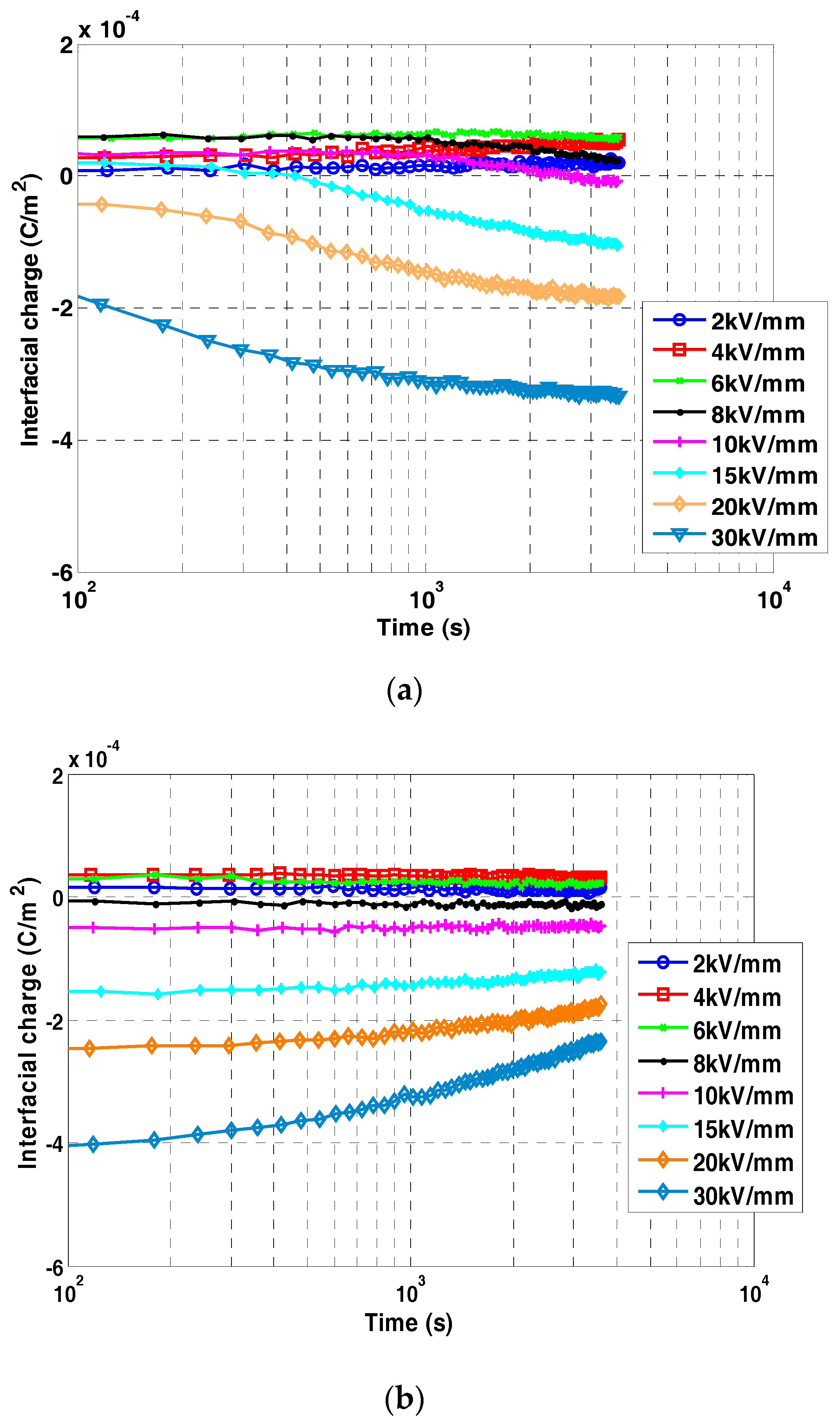
Figure 6 illustrates the results on the transient interfacial charge for a cycle consisting of polarization for 1 h followed by short-circuit for 1 h at each field level. Measurements were achieved at 40 °C. Even if the analysis was not possible for charging/discharging times as long as the one in the model, several observations can be done by comparing Figure 4 and Figure 6.
The results show that a positive interfacial charge settles at low field (2 to 6 kV/mm), changing to negative at an average field higher than 10 kV/mm. The kinetic of charge build-up appears faster with an increase of the stress as well, and the relaxation kinetic is much slower than the charge build-up.
Discrepancies between the model and measurements can have several origins. First, the model is based on conductivity measurements realized on samples of the different materials, for a relatively short polarization time (1 h): the stationary regime is certainly not reached. Second, we have considered that the Maxwell–Wagner process was the sole phenomenon controlling the field distribution, which is not the case by taking into account space charge accumulation in the insulation bulk. Field distribution and temporal analysis of the dielectric behavior are presented in further details in the following.
3.3. Field Distribution
By combining Equations (2)–(4), function of time, one shows that the electric field in both materials has the form:
Experimentally, field profiles are derived from charge profiles by integration of the Poisson’s equation:
where x0 is taken at the beginning of the peak of the image charge in Figure 5. Figure 7 compares the field profiles derived from the model and from the experiments at a temperature of 40 °C, for 1 h of application of the stress.
Results obtained for a temperature of 20 and 70 °C are presented elsewhere [14]. The location of the field maximum is remarkably well predicted: the field maximum shifts from XLPE to EPDM for an applied stress larger than 10 kV/mm. However, the field is not uniform in the bulk of the insulation due to space charge accumulation as pointed out previously. After all, the field computed from the conductivity data is an underestimation of the maximum value of the local stress, which constitutes a limitation of the macroscopic modelling approach and justifies the need to perform direct measurements of the field distribution. Measurements presented in this work and realized on film samples are consistent and can be used to approach a multilayered insulation system with cylindrical geometry, representative of the joint structures of cables [9].
3.4. Interfacial Charge Build-Up and Decay Kinetics
For supporting the discussion on the kinetic of the interfacial charge build-up/dissipation, we have considered the associated time constants. From the simulated interfacial charge in polarization, one can estimate the values of the time constants for charge build-up at different temperatures for several stresses, cf. Figure 8a. The time constant is defined through Equation (6) and is tractable if the field values in the bi-layered system are known. Because this time constant is changing with time, we define it in practice as the effective time such that
which conforms to Equation (5) in the case of materials with linear conductivity. One clearly observes that the effective time constant decreases when the field or the temperature is increased. For example, at 20 °C, the time constant is on the order of 105 s for 4 kV/mm, 5.4 × 10⁴ s for 10 kV/mm, and 4.5 × 10² s for 30 kV/mm. At 15 kV/mm, time constants decrease from 3 × 10⁴ s to 6 × 10² s going from 20 °C to 70 °C. Therefore, the kinetic of the charge build-up is faster at higher field/temperature due to a higher conductivity in these materials.
The time constants for depolarization at 40 °C and 70 °C (Figure 8b) have also been estimated from the simulated interfacial charge (in this case it is the time corresponding to a decrease of the charge by a factor e). At 40 °C, the value of the time constant decreases when the field varies between 2 and 8 kV/mm. Then, it increases from 8 to 15 kV/mm and decreases again with an applied stress larger than 15 kV/mm. At 70 °C, the time constant increases with the stress for stress below 6 kV/mm and decreases for stress above 6 kV/mm. These variations can appear as erratic but they are not: the time constant evolution maps the evolution of the initial amount of interfacial charge. The leading quantity here is actually the residual field radiated by the interfacial charge, which is linked to the time constant through Equation (6). The interfacial charge being the sole contribution to the residual field, it appears straightforward that the kinetic of the relaxation is sensitive to the interfacial charge density.
Therefore, one can conclude that the higher the interfacial charge density, the faster the relaxation dynamic. This explains the observed differences between the time constant in polarization and in depolarization. In polarization, the time constants exhibit similar evolutions at any temperature: they decrease with the applied field. On the contrary, in depolarization the charge relaxation depends on the temperature and on interfacial charge density accumulated in polarization. The applied stress is not acting directly on the kinetic because, as previously emphasized, the interfacial charge can decrease, become null, and can change its polarity when the electric field increases.
4. Discussion
The design of cables and accessories for HVDC systems is more complex when compared to high voltage alternating current (HVAC) systems because it is difficult to predict and control the field distribution within the insulating parts. The results presented here on bi-layered insulations under different electric and thermal stresses are a good illustration of this complexity. They also give a strategy for the design of DC cables joints. The kinetic of charge accumulation is governed by field and temperature conditions. In some cases, the stationary regime is only reached after 10 h of polarization. This time constant may be longer than the characteristic time of fluctuations occurring in the system in service. It concerns fluctuations in current circulating in the cable core (in relation with the variation of energy production/consumption which transit into the cable). Variation in current implies variation in temperature hence field redistribution. A situation with strong charge/field redistribution is the case of polarity inversions that are needed to reverse the power flow in the case of line-commutated converters (LCC) based on thyristor technologies. In these situations, the field distribution in the cable and accessories is out of equilibrium and depends on transient electro-thermal conditions of the system.
Another fact of the results is that a good estimation of the electrical stress distribution in bi-layered dielectrics can be reached if an adequate model of conductivity is used. This can be checked by considering the polarity of the interfacial charge obtained in the measurement and simulation. The charge build-up kinetic and the charge behavior under polarity reversal characterized by PEA are comparable to the simulated results based on conductivity measurements. This comparison is to be critically assessed because the measurements are different in nature (space charge vs. conduction current), tests have not been done on the same samples, and simplified hypotheses have been adopted for the analysis. Moreover, results can differ due to the use of different type of electrodes.
The main reason for discrepancies between measurements and simulation is due to space charge accumulation in the bulk of the materials. Space charge measurements effectively show the presence of internal charges in XLPE and EPDM. At 20 and 40 °C, homocharges are detected near the electrodes due to injection phenomena [14]. Their density increases with the applied field. At 50 and 70 °C, heterocharges are detected near the cathode (in XLPE). This is often explained in XLPE by the presence of cross-linking residues [23,24]. As a consequence, a non-uniform field distribution sets up in the bi-layered sample, especially in XLPE, which explains the underestimation of the field maximum when compared to the field in simulation.
The spatial extension of the interfacial charge is an important question in the measurement as well as in the model. In the PEA method, the apparent width of the peak reflecting the presence of a plan of charges depends on the dispersion of the acoustic waves during their propagation, and therefore on the nature and thickness of the supporting materials. For example, EPDM as an elastomer is more absorbing and dispersive for the acoustic waves than XLPE. In space charge measurements, considering Figure 5, and other results not given in this work, one can note that the width of the interfacial charge peak is about the same as the width of the image charge on the electrodes. It follows that the spatial extension of the interfacial charge does not exceed the spatial resolution of the PEA set-up. A set-up with a higher resolution would be needed to investigate this problem more accurately.
From a physical point of view, the MW model stipulates the charges are supported by a plan which has no physical reality. One has to deal with real charges having necessarily a spatial extension as a result of the equilibrium between diffusion processes (due to the concentration gradient of the charges), trapping, and transport. A more sophisticated model has to be developed to tackle this question, based on a microscopic approach incorporating charge generation at the electrodes, their nature (electrons, holes, ions), their transport in the volume, etc. Such models have been implemented, particularly during the last decade and applied mainly to polyethylene materials [25,26,27,28]. They feature bipolar transport, and consider charge generation at the electrodes, trapping, and recombination. However, mainly electronic carriers have been considered so far, and the association of dielectrics has not been treated to our knowledge. In the above results, we have shown that heterocharge may build-up within the XLPE. Such behavior is also reported in previous studies—see e.g., [8,9] where it is shown also that the semiconductor may be influential in the build-up of such heterocharges. The heterocharge has been reproduced in those models as the result of the formation of deep trap levels in front of the electrodes where (electronic) charges would be extracted [29], of the formation of a barrier to extraction, or of the transport of ionic species [30]. It is clear that macroscopic models have reached their limit for tackling these problems and that recourse to fluid models is necessary to model field distributions in multilayer dielectrics or in cable structures. However, the detailed physics and the identification of parameters remain a difficult task. Perspectives are therefore open to describe more accurately these interfacial charge phenomena.
5. Conclusions
We have shown that space charge measurements allow estimating the interfacial charge due to the Maxwell–Wagner effect between two dielectrics of different natures. Notably, measurements show that the field distribution changes progressively from a capacitive distribution to a resistive distribution for long-term application of the DC stress.
If the amount of measured interfacial charges is globally consistent with the simulated results based on conductivity measurements, discrepancies are observed which are due to space charge accumulation in the bulk of the materials. Therefore, the more general problem of charge trapping in the bulk of insulations has to be addressed. In this problem, models of conduction show their limit and one must develop fluid models and consider elementary processes of charge generation, transport, and trapping. This will impact in turn the way the interface charge is modelled, with, for example, the need to introduce the diffusion contribution to the charge motion.
Finally, it must be noted that time constants for charge build-up can be long, several tens of hours, in such a way that in service the electrostatic equilibrium could never be reached if one considers the daily variation of power flow in the cable.
Acknowledgments
Thanks to Silec-General Cable for providing the samples and supporting part of this study.
Author Contributions
Gilbert Teyssedre and Thi Thu Nga Vu conceived the project; Thi Thu Nga Vu realized the measurements and FEM modelling; Séverine Le Roy contributed to modelling; Christian Laurent and Gilbert Teyssedre wrote the paper.
Conflicts of Interest
The authors declare no conflict of interest.
References
- Eoll, C.K. Theory of stress distribution in insulation of High-Voltage DC cables: Part I. IEEE Trans. Electr. Insul. 1975, 10, 27–35. [Google Scholar] [CrossRef]
- Boggs, S.; Dwight, H.; Hjerrild, J.; Holbol, J.T.; Henriksen, M. Effect of insulation properties on the field grading of solid dielectric DC cable. IEEE Trans. Power Deliv. 2001, 16, 456–462. [Google Scholar] [CrossRef]
- Mazzanti, G.; Marzinotto, M. Extruded Cables for High-Voltage Direct-Current Transmission; Wiley-IEEE Press: New Jersey, NJ, USA, 2013. [Google Scholar]
- Vatonne, R.; Beneteau, J.; Boudinet, N.; Hondaa, P.; Lesur, F.; Denche Castejon, G.; Arguelles Enjuanes, J.M. Specification for extruded HVDC land cable systems. In Proceedings of the 8th International Conference on Insulated Power Cables (Jicable’11), Versailles, France, 19–23 June 2011. Paper A.2.1. [Google Scholar]
- Chen, G.; Hao, M.; Xu, Z.Q.; Vaughan, A.; Cao, J.Z.; Wang, H.T. Review of high voltage direct current cables. CSEE J. Power Energy Syst. 2015, 1, 9–21. [Google Scholar] [CrossRef]
- Murata, Y.; Sakamaki, M.; Abe, K.; Inoue, Y.; Mashio, S.; Kashiyama, S.; Matsunaga, O.; Igi, T.; Watanabe, M.; Asai, S.; et al. Development of high voltage DC-XLPE cable system. SEI Tech. Rev. 2013, 76, 55–62. [Google Scholar]
- Vu, T.T.N.; Teyssèdre, G.; Vissouvanadin, B.; Le Roy, S.; Laurent, C.; Mammeri, M.; Denizet, I. Field distribution in polymeric MV-HVDC model cable under temperature gradient : Simulation and space charge measurements. Eur. J. Electr. Eng. 2014, 17, 307–325. [Google Scholar]
- Fabiani, D.; Montanari, G.C.; Laurent, C.; Teyssedre, G.; Morshuis, P.H.F.; Bodega, R.; Dissado, L.A.; Campus, A.; Nilsson, U.H. Polymeric HVDC cable design and space charge accumulation. Part 1: Insulation/semicon interface. IEEE Electr. Insul. Mag. 2007, 23, 11–19. [Google Scholar] [CrossRef]
- Delpino, S.; Fabiani, D.; Montanari, G.C.; Laurent, C.; Teyssedre, G.; Morshuis, P.H.F.; Bodega, R.; Dissado, L.A. Polymeric HVDC cable design and space charge accumulation. Part 2: Insulation interfaces. IEEE Electr. Insul. Mag. 2008, 24, 14–24. [Google Scholar]
- Bodega, R.; Morshuis, P.H.F.; Smit, J.J. Space charge measurements on multi-dielectrics by means of the pulsed electroacoustic method. IEEE Trans. Dielectr. Electr. Insul. 2006, 13, 272–281. [Google Scholar] [CrossRef]
- Bodega, R. Space Charge Accumulation in Polymeric High Voltage Cable Systems. Ph.D. Thesis, Delft University of Technology, Delft, The Netherlands, 2006. [Google Scholar]
- Bodega, R.; Morshuis, P.H.F.; Nilsson, U.H.; Perego, G.; Smit, J.J. Charging and polarization phenomena in coaxial XLPE-EPR interfaces. In Proceedings of the IEEE International Symposium on Electrical Insulting Materials, Kitakyushu, Japan, 5–9 June 2005; pp. 107–110. [Google Scholar]
- Eichhorn, R.M. A critical comparison of XLPE and EPR for use as electrical insulation on underground power cables. IEEE Trans. Electr. Insul. 1981, 16, 469–482. [Google Scholar] [CrossRef]
- Vu, T.T.N.; Teyssedre, G.; Vissouvanadin, B.; Le Roy, S.; Laurent, C. Correlating conductivity and space charge measurements in multi-dielectrics under various electrical and thermal stresses. IEEE Trans. Dielectr. Electr. Insul. 2015, 22, 117–127. [Google Scholar] [CrossRef]
- Theoleyre, S.; Tobazeon, R. Ion injection by metallic electrodes in highly polar liquids of controlled conductivity. IEEE Trans. Electr. Insul. 1985, 20, 213–220. [Google Scholar] [CrossRef]
- Morshuis, P.H.F.; Bodega, R.; Fabiani, D.; Montanari, G.C.; Dissado, L.A.; Smit, J.J. Dielectric interfaces in DC constructions: Space charge and polarization phenomena. In Proceedings of the IEEE International Conference on Solid Dielectrics (ICSD), Winchester, UK, 8–13 July 2007; pp. 450–453. [Google Scholar] [CrossRef]
- Capps, R.N. Elastomeric Materials for Acoustical Applications; Naval Research Laboratory: Washington, DC, USA, 1989. [Google Scholar]
- Imburgia, A.; Miceli, R.; Riva Sanseverino, E.; Romano, P.; Viola, F. Review of space charge measurement systems: Acoustic, thermal and optical methods. IEEE Trans. Dielectr. Electr. Insul. 2016, 23, 3126–3142. [Google Scholar] [CrossRef]
- Hole, S.; Sylvestre, A.; Gallot Lavallee, O.; Guillermin, C.; Rain, P.; Rowe, S. Space charge distribution measurement methods and particle loaded insulating materials. J. Phys. D Appl. Phys. 2006, 39, 950–956. [Google Scholar] [CrossRef]
- Das, S.; Gupta, N. Interfacial charge behaviour at dielectric-dielectric interfaces. IEEE Trans. Dielectr. Electr. Insul. 2014, 21, 1302–1311. [Google Scholar] [CrossRef]
- Lan, L.; Yin, Y.; Wu, J. Recovery of space charge waveform in multi-layer dielectrics by means of the pulsed electro-acoustic method. Proc. CSEE 2016, 36, 570–576. [Google Scholar]
- Holé, S.; Ditchi, T.; Lewiner, J. Influence of divergent electric fields on space-charge distribution measurements by elastic methods. Phys. Rev. B 2000, 61, 13528–13539. [Google Scholar] [CrossRef]
- Fu, M.; Chen, G.; Dissado, L.A.; Fothergill, J.C. Influence of thermal treatment and residues on space charge accumulation in XLPE for dc power cable application. IEEE Trans. Dielectr. Electr. Insul. 2007, 14, 53–64. [Google Scholar] [CrossRef]
- Anh, T.T.; Roig, F.; Notingher, P.; Habas, J.P.; Lapinte, V.; Agnel, S.; Castellon, J.; Allais, A.; Kebbabi, L.; Keromnès, L. Investigation of space-charge build-up in materials for HVDC cable insulation in relationship with manufacturing, morphology and cross-linking by-products. In Proceedings of the IEEE International Conference on Solid Dielectrics (ICSD), Bologna, Italy, 30 June–4 July 2013; pp. 440–443. [Google Scholar] [CrossRef]
- Alison, J.M.; Hill, R.M. A model for bipolar charge transport, trapping and recombination in degassed crosslinked polyethene. J. Phys. D Appl. Phys. 1994, 27, 1291–1299. [Google Scholar] [CrossRef]
- Le Roy, S.; Segur, P.; Teyssedre, G.; Laurent, C. Description of bipolar charge transport in polyethylene using a fluid model with a constant mobility: Model prediction. J. Phys. D Appl. Phys. 2004, 37, 298–305. [Google Scholar] [CrossRef]
- Lean, M.H.; Chu, W.P.L. Simulation of bipolar charge transport in nanocomposite polymer films. J. Appl. Phys. 2015, 117, 104102. [Google Scholar] [CrossRef]
- Hoang, A.T.; Serdyuk, Y.V.; Gubanski, S.M. Charge transport in LDPE nanocomposites Part II—Computational approach. Polymers 2016, 8, 103. [Google Scholar] [CrossRef]
- Taleb, M.; Teyssedre, G.; Le Roy, S.; Laurent, C. Modeling of charge injection and extraction in a metal/polymer interface through an exponential distribution of surface states. IEEE Trans. Dielectr. Electr. Insul. 2013, 20, 311–320. [Google Scholar] [CrossRef]
- Lan, L.; Wu, J.D.; Yin, Y.; Zhong, Q.X. Investigation on heterocharge accumulation in crosslinked polyethylene: Experiment and simulation. Jpn. J. Appl. Phys. 2014, 53, 071702. [Google Scholar] [CrossRef]
Figure 1.
Field profiles along the radius of a cross-linked polyethylene (XLPE) insulated medium voltage (MV) cable predicted in steady state condition at ambient temperature (20 °C) and under temperature gradients of 5, 10, and 20 °C (outer temperature of 40 °C, conductor temperature of 45, 50, and 60 °C). Model based on the conductivity data used in the current work [7].

Figure 2.
Scheme of the investigated system and adopted labels. d = d1 + d2 is the total thickness; V is applied voltage; V/d is the average applied stress; : interfacial charge.
Figure 2.
Scheme of the investigated system and adopted labels. d = d1 + d2 is the total thickness; V is applied voltage; V/d is the average applied stress; : interfacial charge.

Figure 3.
Field dependence of the current in XLPE and EPDM for temperatures of 30 and 60 °C measured with a 20 cm² electrode area. Symbols: experimental data for 1 h polarization; continuous lines: fit to Equation (1). The dotted lines (1) and (2) represent power laws with exponent 1 and 2, respectively.

Figure 4.
Build-up (a) and relaxation (b) of the interfacial charge at 40 °C according to the model for different applied stress V/d.
Figure 4.
Build-up (a) and relaxation (b) of the interfacial charge at 40 °C according to the model for different applied stress V/d.

Figure 5.
Cartography (a) and profiles (b) of the space charge at 50 °C. The field was applied for 3 h at different stresses (V/d) followed by 1 h in volt-off. (a): The color code gives the scale for the charge density in C/m3. A polarity inversion of the applied stress has been done at the last field step. (b): The profiles are those obtained at the end of the 3 h polarization step. Cathode to the left; Anode to the right. The red dashed lines indicate the integration limits for the estimation of the interfacial charge.

Figure 6.
Build-up (a) and relaxation (b) of the interfacial charge at 40 °C derived from space charge measurements for different stresses V/d.
Figure 6.
Build-up (a) and relaxation (b) of the interfacial charge at 40 °C derived from space charge measurements for different stresses V/d.

Figure 7.
Electric field distributions obtained by the model (a) and by simulation (b) for 1 h polarization time on XLPE/EPDM bilayers at 40 °C under different stresses.
Figure 7.
Electric field distributions obtained by the model (a) and by simulation (b) for 1 h polarization time on XLPE/EPDM bilayers at 40 °C under different stresses.


Figure 8.
Time constants for interfacial charge build-up in polarization (a) and during relaxation (b) for different values of the applied stress at two temperatures.
Figure 8.
Time constants for interfacial charge build-up in polarization (a) and during relaxation (b) for different values of the applied stress at two temperatures.


Table 1.
Coefficient values in Equation (1) describing the conductivity of XLPE and ethylene-propylene-diene monomer (EPDM) as a function of field and temperature [14]. In Equation (1), B(T) = aT + b. Conductivity is in S/m, field is in V/m, temperature is in K.
Table 1.
Coefficient values in Equation (1) describing the conductivity of XLPE and ethylene-propylene-diene monomer (EPDM) as a function of field and temperature [14]. In Equation (1), B(T) = aT + b. Conductivity is in S/m, field is in V/m, temperature is in K.
| - | XLPE | EPDM |
|---|---|---|
| A (S.I.) | 0.8 | 97 |
| Ea (eV) | 1.0 | 0.44 |
| a (m/V/K) | 0 (T < 313 K); −1.3 × 10⁻⁹ (T ≥ 313 K) | 4.8 × 10⁻¹ |
| b (m/V) | 1.38 × 10⁻⁷ (T < 313 K); 5.45 × 10⁻⁷ (T ≥ 313 K) | −5.1 × 10⁻⁸ |
| α | 0.15 | −1.42 |
© 2017 by the authors. Licensee MDPI, Basel, Switzerland. This article is an open access article distributed under the terms and conditions of the Creative Commons Attribution (CC BY) license (http://creativecommons.org/licenses/by/4.0/).
Share and Cite
MDPI and ACS Style
Vu, T.T.N.; Teyssedre, G.; Roy, S.L.; Laurent, C. Maxwell–Wagner Effect in Multi-Layered Dielectrics: Interfacial Charge Measurement and Modelling. Technologies 2017, 5, 27. https://0-doi-org.brum.beds.ac.uk/10.3390/technologies5020027
AMA Style
Vu TTN, Teyssedre G, Roy SL, Laurent C. Maxwell–Wagner Effect in Multi-Layered Dielectrics: Interfacial Charge Measurement and Modelling. Technologies. 2017; 5(2):27. https://0-doi-org.brum.beds.ac.uk/10.3390/technologies5020027
Chicago/Turabian StyleVu, Thi Thu Nga, Gilbert Teyssedre, Séverine Le Roy, and Christian Laurent. 2017. "Maxwell–Wagner Effect in Multi-Layered Dielectrics: Interfacial Charge Measurement and Modelling" Technologies 5, no. 2: 27. https://0-doi-org.brum.beds.ac.uk/10.3390/technologies5020027
Note that from the first issue of 2016, this journal uses article numbers instead of page numbers. See further details here.