On Electrical Discharge Machining of Non-Conductive Ceramics: A Review


Department of High-Efficiency Machining Technologies, Moscow State University of Technology STANKIN, Vadkovskiy per. 3A, 127055 Moscow, Russia
*
Author to whom correspondence should be addressed.
Technologies 2019, 7(3), 55; https://0-doi-org.brum.beds.ac.uk/10.3390/technologies7030055
Submission received: 4 July 2019
/
Revised: 30 July 2019
/
Accepted: 5 August 2019
/
Published: 8 August 2019
(This article belongs to the Special Issue Reviews and Advances in Materials Processing)
Abstract
:The inability of ceramic and nanoceramic processing without expensive diamond tools and with a high-material-removal rate hampers the scope of its potential applications and does not allow humanity to make a full shift to the sixth technological paradigm associated with Kuhn scientific revolutions and Kondratieff’s waves and restrains the growth of the economy. The authors completed a review on the research state of ceramic and nanoceramic processing by electrical discharge machining, which is possibly solved by two principal approaches associated with the usage of standard commercially available machine tools. The first approach is related to the introduction of expensive secondary phase; the second approach proposes initiate processing by adding auxiliary electrodes in the form of coating, suspension, aerosol, or 3D-printed layer based on the components of silver, copper, or graphite in combination with an improved dielectric oil environment by introducing graphite or carbon nanoparticles, which is hugely relevant today.
1. Introduction
By the beginning of the 21st century, ceramics and hard alloys were entirely developed and widely spread in the field of engineering [1,2,3]. It is difficult to imagine modern production in almost all machinery industries without cutting tools or other products made of ceramics and hard alloys. The scope of their applications is extensive but has one distinction—products of ceramic and hard alloys are used in extreme operating conditions under heat and ultimate loads. In this condition, no other material can provide the necessary performance, heat and wear resistance [4,5].
Due to the excellent exploitation properties of ceramics [6,7] and according to the summary analysis of experts, the volume of the world ceramic market grows at an average annual rate of 9.2%, and by 2020, the market volume will reach $103 billion [8,9,10,11]. The trends for nanoceramics can be even more significant in further perspective. According to the results of recent studies [12,13], the samples of nanoceramics obtained by improved hybrid spark plasma sintering can exceed in main operational parameters (such as hardness, crack and wear resistance) of technical ceramics sintered by traditional isostatic pressing with subsequent vacuum sintering by 30%. The specialists of the subject area associate this phenomenon with the Hall–Petch relation, which describes the growth of the yield strength of a polycrystalline material with a decrease in the grain size [14,15].
However, the introduction of nanoceramics into real life is limited because of their high costs and low workability. The manufacture of each product requires high costs and is very labor-intensive. It requires fewer allowances in processing and the purchase of precision cutting tools based on artificial diamond, as cutting tools made of traditional alloys are worn extremely fast. In its turn, the geometry of cutting tools limits the resulting geometry of the product. Other machining methods such as vibroacoustic machining, laser and electron beam scribing, selective laser sintering with a binder, find their specific place in the processing of ceramics. However, they do not allow the receiving of all geometrically possible shapes of the product without losses on the operational parameters of ceramics [16,17,18].
One of the most popular methods for the production of parts, regardless of their hardness, is electrical discharge machining (EDM). However, it requires the material to be conductive [19,20,21]. The process of electrical erosion of the material consists of initiating electric pulses in the interelectrode gap, in the breakdown of the dielectric medium in the gap, in establishing a discharge channel, where the temperature reaches more than 10,000 °C (low-temperature plasma). Due to such temperatures, the material is ablated, the drops of cooled material as eroded debris are washed away by the flow of the dielectric medium, and the electrodes again approach to resume the cycle. Thus, a unique crater-like topology on the surface of the workpiece is created [22,23,24,25].
The inability of ceramics and nanoceramics to conduct current hampers the scope of its potential applications and restrains the growth of the progress and the switch to the next technological paradigm that most of the scientists associate with the term “nano” [26,27,28,29,30,31,32].
Thus, it can be concluded that the study and development of a method for electrical discharge machining of non-conductive ceramics and nanoceramics are incredibly relevant today.
The authors propose to apply the dialectical approach of cognition as a scientific approach to solve the formulated scientific problem. The dialectical approach includes the systematization and updating of existing knowledge and new data about the object of research.
2. Scientific Problem
The scientific problem of the physical impossibility of superhard ceramic materials machining (as the exception is the diamond grinding method) is considered because of their nearly zero conductivity since the electrical conductivity of ceramics, as for all solids, depends on the concentration of charge carriers, their magnitude, and mobility. The material conductivity is composed of each its constituent phase electrical conductivity: The measurement of the electrical conductivity of especially pure oxide ceramics becomes a complex scientific and technical problem. In many cases, the problem is the impossibility of obtaining the necessary complex spatial geometric shape of surfaces of functional products from high-strength ceramics by traditional methods of processing. There is a strong need of the development of a new inexpensive way of ceramic nanocomposites machining.
There are two main approaches to solving this problem to achieve this goal:
- -
- The creation of a new class of nanocomposite ceramics with the inclusion of the conductive phase allowing the machining of blanks in order to obtain the finished product with the use of minimal technological effort and the absence of direct contact between the material and tool, i.e., using the electric discharging methods of machining [33,34,35,36,37,38,39];
- -
- The modification of the surface layer of the nonconducting workpiece, the geometric shape of which is already close to the geometry of the final product, by applying a conductive coating (auxiliary electrode) with a thickness of ~20 μm, which could become an intensifier of electrical discharge machining of non-conductive ceramics [40,41,42,43,44].
The second approach is the less expensive and may have a high level of technological adaptation to the conditions of real machine-building production, and is capable of producing positive results on a large scale. First of all, these conclusions are related to favorable technological conditions for the sintering of single-phase nanoceramics from the relatively low cost of ZrO2 and Al2O3 nanopowders in comparison with the cost of the nanoscale modified electrically conductive phases (for example, graphene, graphene oxide). The other reason is the relatively low cost of materials for the production of a profile tool for EDM.
The design of constructive and technological features of the product allows the withdrawal of the application of superhard materials such as nanoceramics based on ZrO2 and Al2O3 on a new production level [45,46,47,48]. It contributes to their spread in the industry for creating a new class of wear-resistant parts, which are capable of operating under extreme operating loads without losing their performance. That is extremely important in solving tasks of the transition to advanced intellectual production, new materials, and methods.
3. Current State of Research
3.1. The Main Scientific Competitors
The research subject is connected to the research of the method of applying EDM to the processing of nanoceramics made by advanced sintering technologies. The analysis of the leading world scientific competitors in this domain shows that the world community is separated as it was mentioned above. One group of scientists is focused on the modification of nanoceramics with conductive inclusions to create systems such as ZrO2-Ta, ZrO2-TiC, ZrO2-TiCN, Si3N4-TiC, Si3N4-TiCN, Al2O3-TiC, Al2O3-TiCN [49,50,51,52,53,54,55,56,57,58,59], as well as inclusions based on graphene and oxide graphene and graphene nanotubes [23,60,61,62,63,64]. Another group of scientists has focused their research on the processing capabilities of existed ceramics and non-conductive ceramic composites. The processing ability (ability to EDM) of such ceramics can be modified by introducing an auxiliary electrode based on copper, brass, steel, carbon, etc. in the form of particles, nanoparticles or thin-film in the process of electrical discharge machining. In this case, an auxiliary electrode will play the role of an initiator and intensifier of technology.
One of the most successful examples of such work is the work of the scientists at the Universities of Chemnitz and Freiburg and their colleagues at the Toyota Concern [65,66,67,68]. The research team at Chemnitz Technical University (Germany) under the guidance of Prof. Andreas Schubert have worked on the processing of insulating materials [23,69]. In particular, they propose replacing expensive diamond cutting with micro electrical discharge machining (µEDM) for specific technical applications. The researchers obtained a result on the µEDM of technical oxide and nitride ceramics (ZrO2, Si3N4-TiN, and others). In this case, the copper electrode moved progressively along the surface, following the developed control program of CNC-machine. The electrode tool motion looks like kinematic motion of milling cutter during 3-axis milling of grooves and pockets.
The search for alternative methods of processing non-conductive materials was also conducted at the University of Freiburg (Germany) [70]. The authors described two technologies for forming an auxiliary electrode in the form of a coating: Applying a suspension of gas soot and polymethyl methacrylate (PMMA, organic glass or acrylic) by hand and applying the suspension by direct printing carbon conductive ink (C-W) on a commercially available Ekra M2 printer. The coating was carried out on cylindrical samples of non-conductive technical ceramics ZrO2. As a result, the fundamental possibility of initiating EDM was proved; eroded debris were involved in processing. However, the authors proposed to use both methods exclusively for super-precision low-cost final finishing since the specific material removal rate could be characterized as modest in comparison with traditional EDM of metals. In their work, the authors criticized the use of plasma-vacuum coating as an initiator of EDM because of its high cost and inaccessibility. The authors of the article, in turn, referred to the successful experience of their Japanese colleagues, in particular, the results of Prof. Mohri.
In Japan, with the cooperation of such scientific schools as the Technological Institute of Toyota, The Technological University in Nagaoka and the Technological College in Tsukuba, in the 1990s, a team of scientists was formed under the guidance of the eminent Prof. Naotake Mohri, with the participation of Prof. Katsushi Furutani. In 1996, this group [71] proposed a new method of EDM of dielectric ceramics, by applying an auxiliary electrode in the form of a metal grid on the surface being machined. The EDM was carried out with a brass or copper electrode using kerosene as a working fluid. Prof. Mohri continues to publish the results of research as part of the same research team [72], in which work is underway to develop a method for applying a conductive coating for ceramics based on crystallized carbon or carbides and working oil, and explores the phenomenon and mechanisms of initiation and acceleration of electrical erosion of a non-conductive substance.
Their colleagues from the Council for Scientific and Technical Research of Turkey, under the guidance of Prof. Can Çoğun, obtained other impressive results: The process of coarse electrical discharge and electrochemical machining of non-conductive materials KTU-1, TiO2, glass, ZrO2 (with the addition of Y2O3), and Al2O3 by adding carbon particles no larger than 30 microns in a dielectric liquid (kerosene) [73,74,75]. The treatment was carried out using an electrode in the form of a hollow copper tube (a diameter of 3.5 mm). Thus, it was possible to drill the rough holes in workpieces of various shapes, their geometry was obviously faulted, perhaps due to the lack of reliable fixation of spherical blanks on the machine’s worktable; the experiment with Al2O3 turned out to be especially unsuccessful.
The research on the processing of non-conductive materials was also conducted at several research centers in Malaysia. The work published by the research team under the supervision of Dr. Muhammed Abdul Maleque at the International Islamic University of Malaysia (Kuala Lumpur) [76] demonstrated the results of the processing of technical ZrO2, wholly covered with a casing of platinum copper. The obtained result proved the ability and effectiveness of EDM processing in kerosene; copper residues from the surface of the ceramic workpiece were successfully removed. Another Malaysian group of scientists under the supervision of Dr. Mohd Amri Lajis at the Technical University of Malaysia (Malacca) in cooperation with the University of Malaysia described the result [77,78] where an acrylic blank was machined by placing an electrode inside a steel sleeve of 15 mm in diameter. Thus, the authors obtained a conical hole in the non-conducting material following the geometry of the electrode.
The research in the field of EDM processing of dielectric materials is carried out at the Perm National Research Polytechnic University under the supervision of Dr. Timur Rizovich Ablyaz. The authors theoretically and practically investigated the principal ability of EDM processing of non-conductive materials as Al2O3+ZrO15 ceramics by initiating a discharge channel by placing the erosion products in the interelectrode gap [79,80,81]. The authors provided an analysis of the EDM methods for dielectric materials and considered modern approaches to optimize technologies proposed by previously mentioned colleagues. Their ideas deserve attention and detailed experimental approbation.
3.2. Production of Nanoceramics by Advanced SPS
Today the most sought-after researchers are focused on creating new nanomaterials by advanced spark plasma sintering (SPS) [37,39,82,83,84]. The development and creation of new progressive nanocomposite materials based on ceramic-ceramic and metal-ceramic compositions strengthened with metal nanoparticles and carbides, carbon nanotubes and nanofibers, graphene and graphene oxide are popular due to improved physical and mechanical properties and chemical inertness. The mathematical models developed for SPS assist in the controlling of properties of new materials [85,86,87].
A technical concept for creating a new class of nanocomposites by spark plasma sintering [88,89,90,91,92] includes the principles of interfacing the components of an innovative spark plasma sintering system, components of a high-current source node equipped with a pressure and temperature controller, and calibration.
Structural nanoceramics can have gradient properties according to particular customer requirements. The developed concept of creating nanocomposite gradient materials consists of creating a new functional mold and using low sintering temperature to minimize residual stresses [93]. The nanostructured powders for this kind of material are prepared according to the known scheme by colloidal processing [37,39].
As is known, one of the critical parameters for sintering materials is the distribution of temperature fields over the entire volume of the sintered product [94,95]. For this reason, the achievement of a uniform distribution of temperature fields in volume is a critical point in the design of tooling and die. Thus, a new model of semi-molds for sintering was designed [37]. The device contains a die of heat-resistant conductive material, insulating a sleeve made of heat-resistant heat-conducting and non-conductive material, a lower punch made of heat-resistant conductive material, an upper punch consisting of two heat-resistant conductive concentric parts, separated by an insulating material. At the same time, punches are processed, and the composition of powder materials is separated through gaskets. This new design allows changing the flow of electrons flowing through the die and, thereby, ensuring its heating. When the percolation of the sintered material is reached, the electrons begin to flow through both the die and the powder material to be processed. Thus, uniform heating of the product throughout its volume is achieved.
Simulated physical processes in order to optimize the technology can help to study the process of sintering and develop solutions for the problems related to the creation of new materials. As part of the study of the problems of technological development for the synthesis of new nanostructured materials by the method of spark plasma sintering, a theoretical description of the sintering process using methods of mathematical and theoretical physics, based on the theory of density functions and nucleation theory, the Keldysh method for electron transfer in a medium consisting of a conglomerate of nanocatrices (tungsten, aluminum and titanium alloys), with additions in the form of crystalline and amorphous mesostructures, causes genuine interest. This method is currently developed in detailed mathematical models of heat and mass transfer in areas of axisymmetric complex shapes of rotation bodies (in connection with the problems of modeling nozzles and nozzles of rockets, aircraft engines). However, with the parameters of the spark plasma sintering process—pulse duration in the range from 1 to 250 ms, average sintering pulse power up to 150 kW, and heating of the mold with powder material up to 2000 °C—new approaches are needed to solve the mass transfer equations, vibrational equations, and temperature distributions, with singular parameters of the substance, thermal conductivity and heat capacity, and time modulated by short pulses of sintering current of extra-large power. In this regard, the problem can be solved by simulating a substance in a cylindrical sintering area by directly pulsing the current through a mold with powder material and additional induction heating and obtaining the microphysical parameters of powder materials using the method of asymptotic approximation and singular generalized functions.
Since in the process of pulsed sintering in the mold, nanoparticles of metals (W, Ti, Al) and crystalline nanostructures (nanotubes, graphene, graphene oxides, nano-diamonds) with a particle size of 50 to 500 nm pass through a characteristic time of several tens of phase transformations, with diffusion and threshold processes for the transfer of molecules and electrons, the result of sintering and the physical properties of the substance obtained are not predictable without precisely setting and modeling the initial data and the dynamic behavior of the physicochemical properties of particles during the sintering process.
Preliminary experimental models were developed that use a Langmuir probe, an optical probe–waveguide to remove the spectral characteristics of the plasma during sintering, for measuring the phases of the voltage and current of the sintering pulse to study these properties. The main theory explaining the physicochemical properties of the material obtained after the action of a series of pulses is the theory of the growth of germ clusters and nucleation (Frenkel–Landau).
In the course of the work for the investigation of the process of pulsed sintering, new effects that were not previously considered in international literature were found: Accelerated nucleation, electronic nanojet, nanofilament, and photon nanojet in the field of thermal photons. At present, an important physicochemical process of reducing the threshold power of electronic breakdown for sintering conglomerates of dielectric nanoparticles by introducing additional impurities from metallic conductive nanoparticles was found and studied. It should be noted that for these processes there are important optical analogs. In the visible and infrared range, there is a new effect, not previously considered as an application to the process of a pulse, as well as a laser sintering effect—the photon nanojet (photonic nanojet). This effect is used as an analog of the electronic jet, the spatial effect of high electron density on the surface of nanoparticles, due to the excitation of the Frohlich modes to simulate the sintering processes. In addition to the theoretical study of nonlinear effects, in the process of pulsed sintering, there is the possibility of the practical application of a photon jet for a wide range of technical applications as a working medium for microlasers, microlenses, radiation detectors, and metamaterials. Interest in the considered processes takes place in the microwave field, in the calculation and design of metamaterials for the microwave coatings of airplanes and rockets, as well as in the calculations of thermal protective coatings.
The properties of sintered Al2O3-TiC-Ni nanocomposite in comparison with the properties of a sample of aluminum oxide (Al2O3) obtained by hot pressing—the traditional sintering method exceed them due to smaller alumina grains [39]. The average particle size of the aluminum oxide powder in the nanocomposite is approximately 0.3 ± 0.1 μm, while in a monolithic material this size is 3 ± 1 μm. The structure of the Al2O3-TiC-Ni nanocomposite contains Ni and TiC nanoparticles. Although the process of sintering occurs at a temperature of 1375 °C, the nanoparticles do not significantly increase in size. The hardening of the nanocomposite was expected due to the presence of Ni nanoparticles. The measured relative density of the samples was >98%. The difference in wear resistance between Al2O3 and Al2O3-TiC-Ni nanocomposite under dry slip conditions depends on the hardness of the material, as well as the size of the aluminum oxide grains in the nanocomposite. Both parameters are most important for improving the tribological properties in working conditions.
3.3. Classification of Technical Ceramics and Its Workability by EDM
Technical ceramics are classified based on functionality such as biocompatibility, electrical properties, optical properties, mechanical strength, and resistance to high temperatures according to the following types: Medical ceramics; electroceramics; optical ceramics; structural ceramics and ceramics for extreme conditions; ceramics for energy transfer, storage and conversion; and other types of ceramics [96,97].
It should be noted that high-tech industries are experiencing an acute shortage in the production of ceramic materials and high-tech products made from them, which have high performance properties.
On the one hand, this is due to the use of outdated technologies in production and the lack of knowledge in obtaining advanced high-strength ceramic nanomaterials and composites based on them, and on the other hand, using outdated technologies for processing ceramics. The most advanced production is directly dependent on suppliers of equipment and limited in the choice of technological processing modes. This undoubtedly endangers the adequate response to modern challenges.
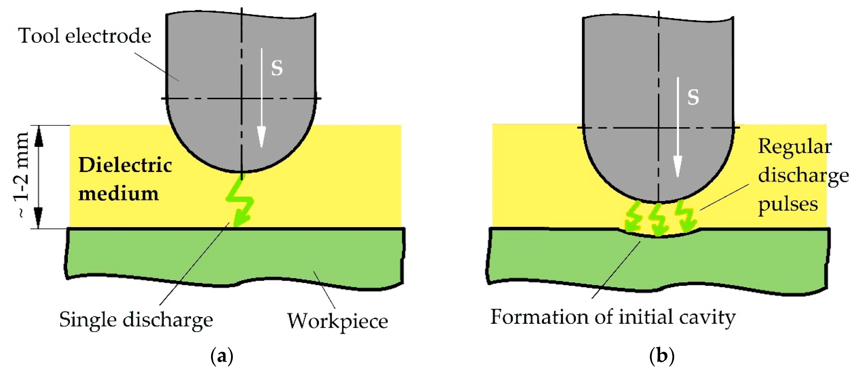
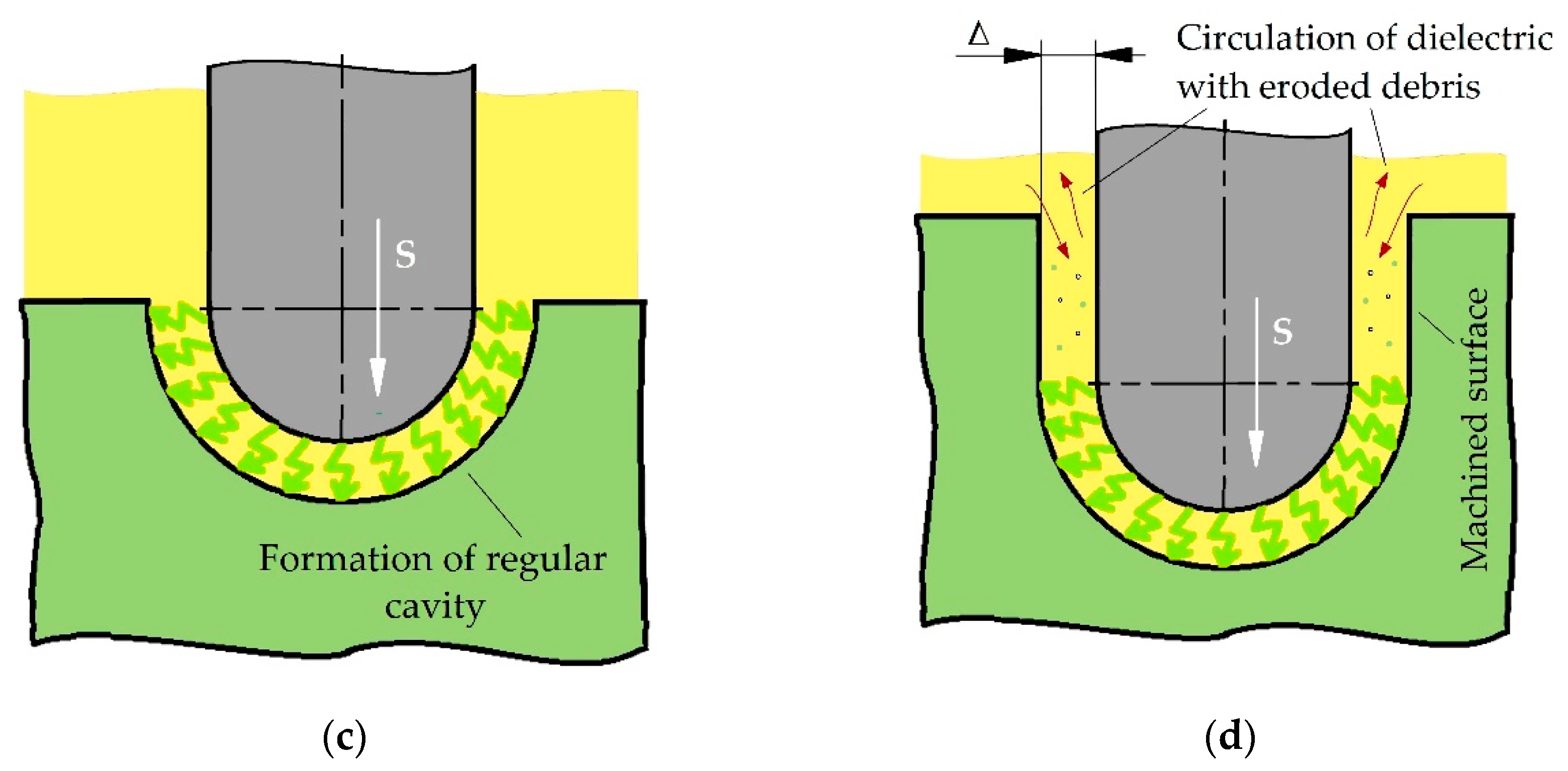
Electrical discharge machining is a highly efficient method of processing electrically conductive materials regardless of their mechanical properties (Figure 1). The schematic presentation of the electrical erosion steps under discharge pulses is shown in Figure 2. The regular discharge gap forms on the surface of the workpiece during the formation of the cavity to be processed: Two electrodes approach up to the moment of first working discharges, which transforms into the discharge channel (Figure 1a). Then the tool electrode advances in the cavity formed by the first discharges (Figure 1b) and creates a regular cavity in the workpiece (Figure 1c). On this stage, the pulses acting between the two electrodes balance each other (Figure 1d), and electrical discharge machining becomes stable.
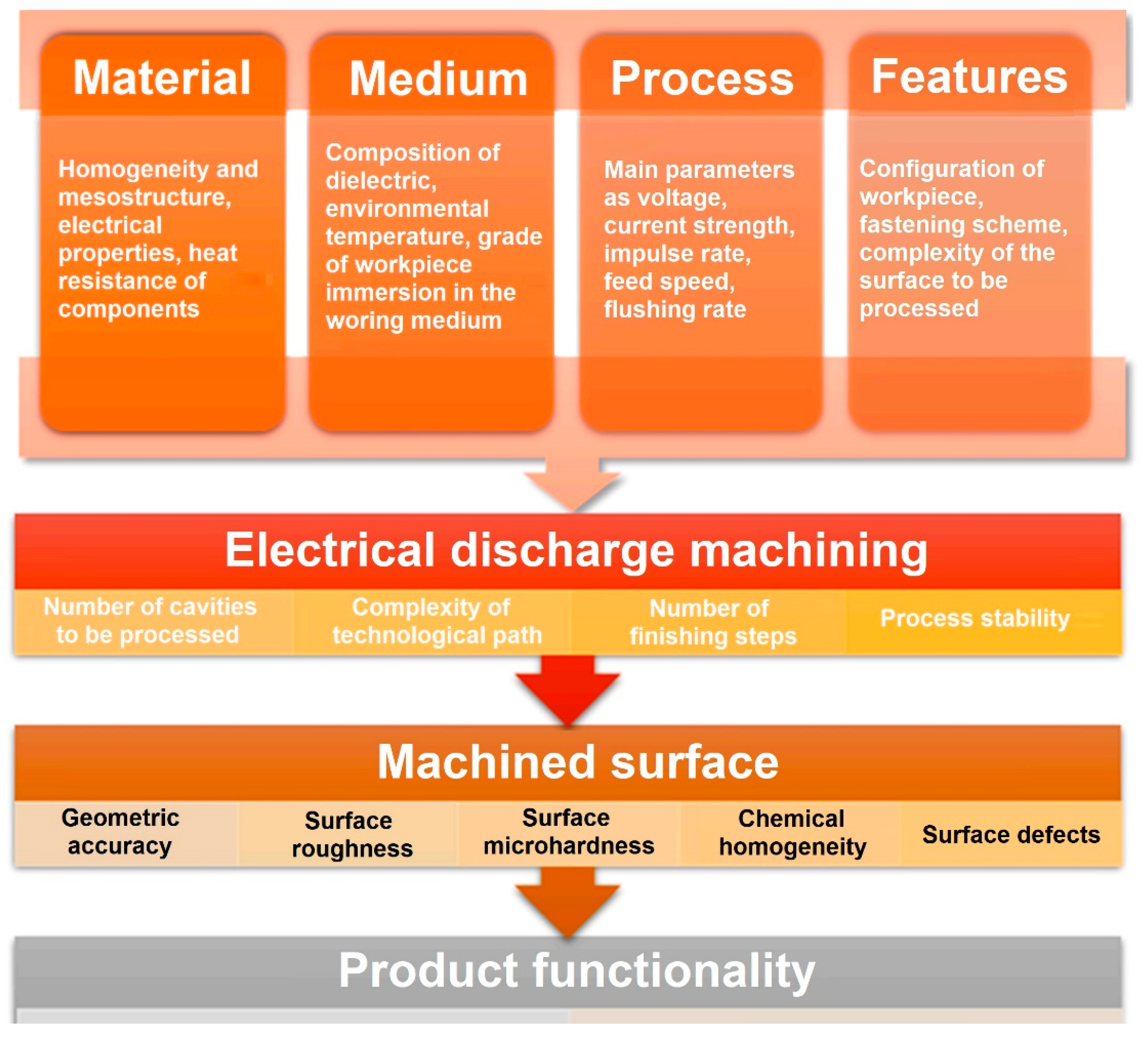
Modern scientists divide the main processing factors that influence the results of electrical discharge machining into four main groups [24,25,98,99] (Figure 3):
- factors related to the material of electrodes (e.g., homogeneity, conductivity for a tool and a workpiece, heat resistance of the material components);
- factors related to the environment (e.g., temperature, dielectric composition, a grade of workpiece immersion into the fluid);
- factors related to machining process and controlled by CNC-system (e.g., operation voltage, strength of the operational current, auxiliary voltage, strength of the auxiliary current, operational and auxiliary impulses rate, electrode feed, the dielectric pressure in nozzles);
- factors related to technological features of processing (e.g., scheme and system of workpiece fastening, configuration of the workpiece, complexity of surface to be processed).
All these factors influence the stability of EDM. The quality of the processed surface can be controlled by measuring final geometrical accuracy, roughness, microhardness, change of chemical content in subsurface layer (up to the depth of ~4–10 µm), homogeneity of the processed surface, and an absence of the visible defects, which can influence the final product appearance and functionality. In this case, the product functionality can be presented as a complex, which consists of its operational ability as part of a more sophisticated unit such as a mechanism or machine and its appearance following customer requirements.
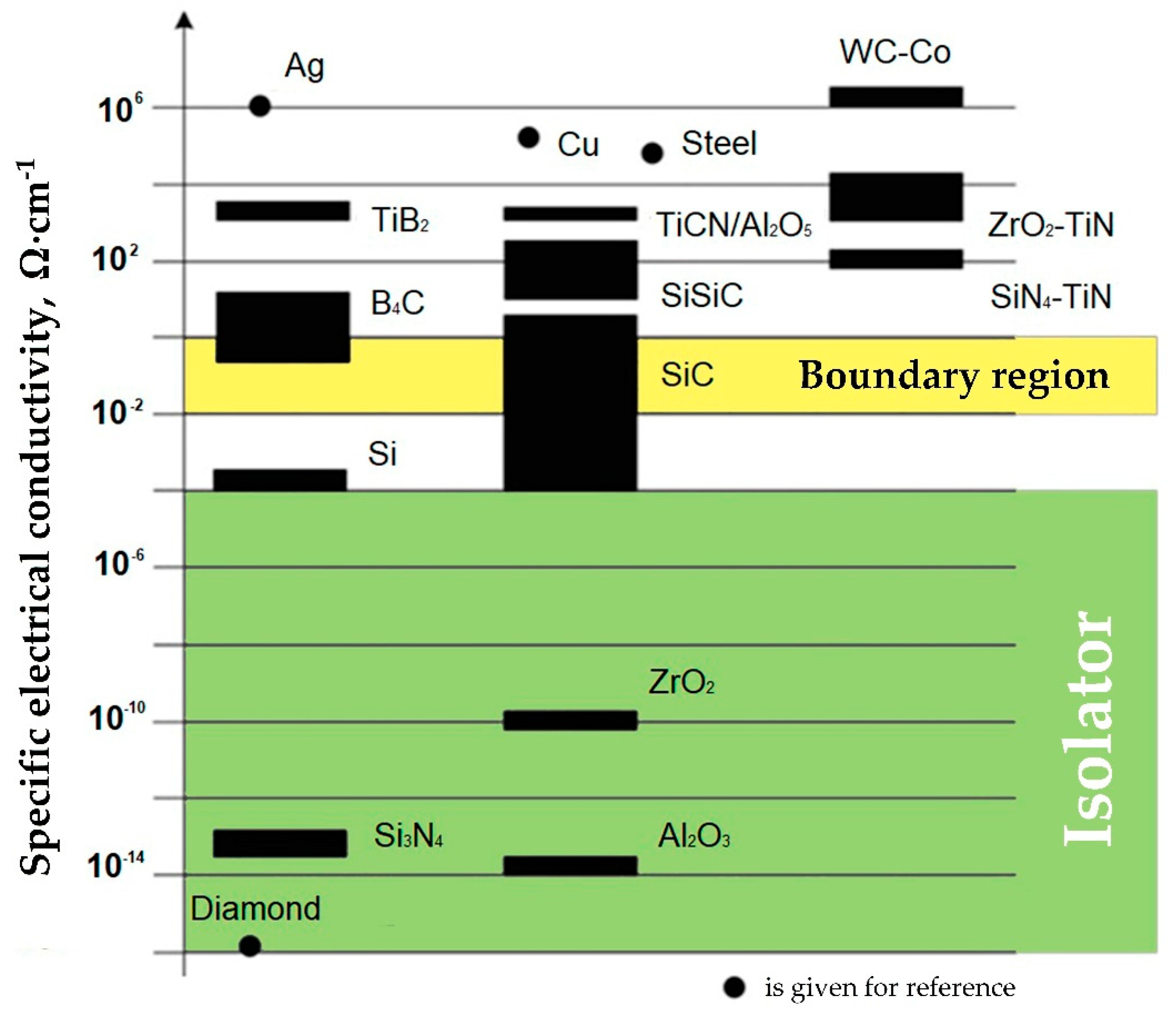
EDM is possible only if the minimum electrical conductivity of materials is about 10-2 Ω·cm-1. The electrical conductivity of the material is a critical factor in the success of the process of electrical erosion. All metals fulfill the condition in terms of minimum electrical conductivity, which is not the case with ceramics and its composites. Figure 4 shows the main ceramic materials, depending on their conductivity. Electrically conductive ceramics such as SiC, TiB2, TiN, and TiC are treated with EDM, while the electrical conductivity of Al2O3, ZrO2, Si3N4 is not enough to initiate processing. As it was mentioned before, at present, two different ways of processing non-conductive ceramics by EDM are used:
- 1)
- Doping ceramics with an additional electrically conductive phase;
- 2)
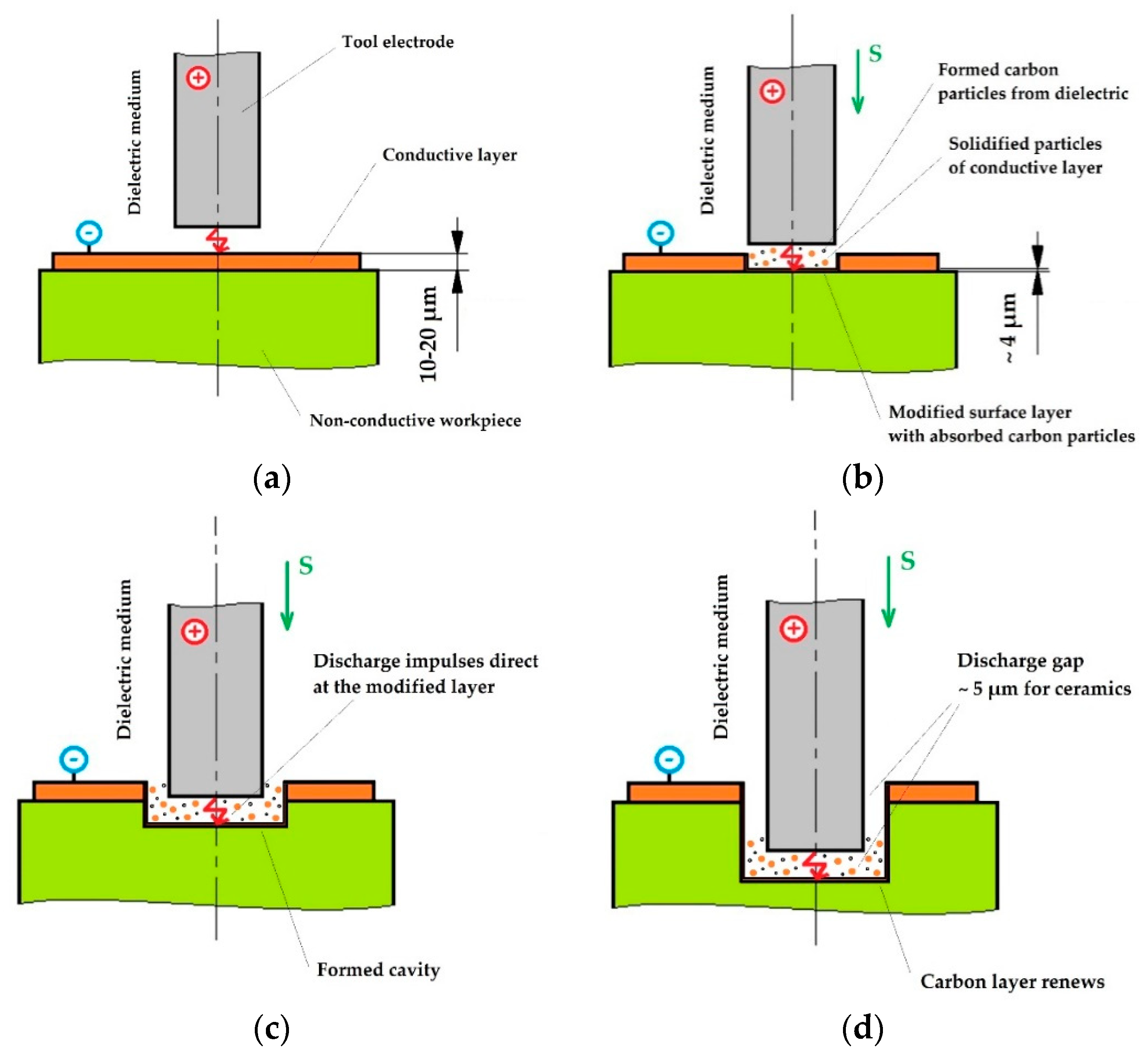
- Deposition of an electrically conductive coating on the surface of the non-conductive ceramics, initiating the start of interaction and initiation of the first sparks. The authors propose to use the second approach in the research and development of a method for processing non-conductive ceramics and composites as it can help to introduce available up-to-date solutions for the machining of ceramics without the additional costs of a second conductive phase of ceramics, which can reduce the exploitation properties of ceramics (Figure 5).
4. Discussion
An analysis of the current state of research on this issue and the main guidelines of research in world science showed that the world community is focused mainly on the modification of nanoceramics with current-conducting inclusions to create systems of the type “oxide or nitride ceramics—conductive additives”. As well, the most popular but extremely expensive inclusions today for the production of a material system with advanced exploitation properties are nanotubes of graphene and graphene oxide [28,56].
Despite the efforts of the world scientific community to solve the global problem of processing non-conductive ceramics and nanoceramics due to the inclusion of the secondary phase, the issue remains unresolved [34,37,47,48,50,51,88,102]. The main issue that hampers the advances is related to the material of the secondary phase, which often is not widely available for use in the conditions of real production [33,34,36,37,40,44,89,103]. Besides, the material of the secondary phase can significantly change the appearance of ceramics, such as transparency and color, which directly affects and restricts the areas of its potential application [7,8,39,104].
In parallel with the mentioned approach, the world’s leading scientists work on the feasibility of processing technical ceramics by including an initiator and intensifier of the process in the form of an auxiliary electrode based on copper, brass, steel, carbon inclusions, etc. [15,23,35,43]. The additional electrode can be presented in the form of coating deposited by different techniques (including thermal spray and coating technologies or by aerosol, 3D-printing, or drying suspension disposed at a workpiece) or in the form of carbon particles introduced into the processing zone. Suspension can be based on the components of silver, copper, or graphite. A dielectric oil environment can be improved by adding graphite particles and nanoparticles (carbon, graphene nanotubes) in combination with a conductive coating or thin film (up to ~4 µm) or aerosol nanoparticles, which is exceptionally relevant today [15,38,42,43,44,47].
The developed method of the precision shaping of functional products will subsequently contribute to the introduction and distribution of structural nanoceramics in the machine-building industry. It can significantly vary available shapes and properties of nanoceramics regardless of their conductive ability.
The problem of EDM of ceramics needs a fundamentally new approach to find a way of processing by using an economically available solution for direct individual production. Today, the usage of a specially developed conductive coating or thin film with a thickness of ~10-20 μm based on the suspension can be one of the technically available solutions.
The presence of this coating will initiate discharges at non-conductive material. The temperature in the discharge gap can reach 10,000 °C, which is suitable for processing any matter. The presence of carbon particles in the oil medium and the eroded debris, which contain the carbon formed from the organic medium, will contribute to processing.
For example, in the case of processing naturally widely available oxide ceramics such as ZrO2 and Al2O3, their melting points are of 2715 °C and 2054 °C, respectively [33,49,50,68]. The introduction of an additional process initiator can result in the physical ablation of the ceramics with the formation of the conductive form ZrC and unstable compound Al4C3, which can theoretically assist processing.
This method can be called superior to the proposals of its competitors in terms of its use for processing structural nanoceramics. The development and application of the technique can contribute to widespread structural nanoceramics in such industries as aircraft and aerospace, where resistance to the heat and wear is relevant. The processing of nanoceramics with the usage of standard mechanical equipment such as EDM without adding an expensive secondary phase can significantly reduce the cost in manufacturing to surpass any potential manufacture competitors by several times.
5. Conclusions
5.1. Research Work
Based on the results of the research and obtained experimental and analytical results described above, a conductive coating with a thickness of ~10-20 μm for use as an initiator and intensifier of electric erosion corresponds to general world trends. Its application to technical ceramics and nanoceramics in addition to the refusal to modify nanoceramics itself using an expensive conductive secondary phase, which hampers the switch to the next technological order, will allow an advanced and accessible development, in all respects, of a way of processing structural and non-conductive nanomaterials without the loss of their original operational properties such as high resistance to the heat and abrasive wear. In perspective, it can allow the mechanical engineering industry to shift to a new paradigm of production related to the application of nanomaterials, which is unique in its performance properties in terms of its thermal stability and wear-resistance.
5.2. Future Work
Further experiments with the processing of innovative nanoceramics can give a fundamentally new development for the presented idea. It will reveal the principal ability of processing non-conductive oxide nanoceramics and allow the identification of specific conditions and technological modes, and will draw conclusions about the fundamental laws of the main EDM parameters’ influence on the workability of nanoceramic workpieces. That is necessary to form a unique geometry of the typical product sample, for which the solution of the global problem of the operational ability for non-conductive materials is critical. It is important to promote the switch to the next technological paradigm with the elaboration of a new accessible method to process innovative ceramics with equipment, which is widely available at modern mechanical production enterprises.
Author Contributions
Conceptualization, M.V.; Methodology, A.O.; Software, N.K.; Validation, P.P.; Formal Analysis, Y.A.M.; Investigation, A.O.; Resources, Y.A.M.; Data Curation, N.K.; Writing-Original Draft Preparation, P.P.; Writing-Review & Editing, A.O.; Visualization, P.P. and N.K.; Supervision, M.V.; Project Administration, M.V.; Funding Acquisition, Y.A.M.
Funding
This research was funded by the Ministry of Education and Science of Russian Federation, grant number No. 9.7453.2017/6.7.
Acknowledgments
The research was done at the Department of High-Efficiency Machining Technologies of MSTU Stankin.
Conflicts of Interest
The authors declare no conflict of interest.
References
- Grigoriev, S.N.; Kozochkin, M.P.; Sabirov, F.S.; Kutin, A.A. Diagnostic Systems as Basis for Technological Improvement. Procedia CIRP 2012, 1, 599–604. [Google Scholar] [CrossRef] [Green Version]
- Grigoriev, S.; Metel, A. Plasma- and beam-assisted deposition methods. NATO Sci. Ser. 2004, 155, 147–154. [Google Scholar]
- Kozochkin, M.P.; Porvatov, A.N.; Sabirov, F.S.; Kozochkin, M. The fitting of technological equipment with data-measuring systems. Meas. Tech. 2012, 55, 530–534. [Google Scholar] [CrossRef]
- Hameed, S.; Rojas, H.A.G.; Benavides, J.I.P.; Alberro, A.N.; Egea, A.J.S. Influence of the Regime of Electropulsing-Assisted Machining on the Plastic Deformation of the Layer Being Cut. Materials 2018, 11, 886. [Google Scholar] [CrossRef]
- Volosova, M.; Grigoriev, S.; Metel, A.; Shein, A. The Role of Thin-Film Vacuum-Plasma Coatings and Their Influence on the Efficiency of Ceramic Cutting Inserts. Coatings 2018, 8, 287. [Google Scholar] [CrossRef]
- Gallo, L.S.; Boas, M.O.V.; Rodrigues, A.C.; Melo, F.C.; Zanotto, E.D. Transparent glass–ceramics for ballistic protection: materials and challenges. J. Mater. Res. Technol. 2019, 8, 3357–3372. [Google Scholar] [CrossRef]
- Naveau, A.; Rignon-Bret, C.; Wulfman, C. Zirconia abutments in the anterior region: A systematic review of mechanical and esthetic outcomes. J. Prosthet. Dent. 2019, 121, 775. [Google Scholar] [CrossRef]
- Panzani, A. Globalisation Scenarios in the World Ceramic Tile Market Extract of the speach given by Alfonso Panzani at QUALICER CFI Ceram. Forum Int. 2014, 91, E20. [Google Scholar]
- Pascariu, P.; Homocianu, M. ZnO-based ceramic nanofibers: Preparation, properties and applications. Ceram. Int. 2019, 45, 11158–11173. [Google Scholar] [CrossRef]
- Roata, I.C.; Croitoru, C.; Pascu, A.; Stanciu, E.M. Photocatalytic coatings via thermal spraying: A mini-review. AIMS Mater. Sci. 2019, 6, 335–353. [Google Scholar] [CrossRef]
- Xie, S.; Xu, J.; Chen, Y.; Tan, Z.; Nie, R.; Wang, Q.; Zhu, J. Indentation Behavior and Mechanical Properties of Tungsten/Chromium co-Doped Bismuth Titanate Ceramics Sintered at Different Temperatures. Materials 2018, 11, 503. [Google Scholar] [CrossRef]
- Killinger, A.; Gadow, R.; Kern, F. Manufacturing of nanocomposite structural ceramic materials and coatings. Int. J. Mater. Prod. Technol. 2009, 35, 334–345. [Google Scholar]
- Volosova, M.A.; Grigor’ev, S.N.; Kuzin, V.V. Effect of Titanium Nitride Coating on Stress Structural Inhomogeneity in Oxide-Carbide Ceramic. Part Action of Heat Flow. Refract. Ind. Ceram. 2015, 56, 91–96. [Google Scholar] [CrossRef]
- Guo, D.; Song, S.; Luo, R.; Goddard, W.A.; Chen, M.; Reddy, K.M.; An, Q. Grain Boundary Sliding and Amorphization are Responsible for the Reverse Hall-Petch Relation in Superhard Nanocrystalline Boron Carbide. Phys. Rev. Lett. 2018, 121, 145504. [Google Scholar] [CrossRef] [Green Version]
- Balokhonov, R.R.; Zinoviev, A.V.; Romanova, V.A.; Batukhtina, E.E. A Mesomechanical Analysis of the Deformation and Fracture in Polycrystalline Materials with Ceramic Porous Coatings. AIP Conf. Proc. 2015, 1683, 20020. [Google Scholar]
- Murzin, S.P.; Balyakin, V.B. Microstructuring the surface of silicon carbide ceramic by laser action for reducing friction losses in rolling bearings. Opt. Laser Technol. 2017, 88, 96–98. [Google Scholar] [CrossRef]
- Kuzin, V.V.; Seleznev, A.E.; Fedorov, S.Y. Effect of conditions of diamond grinding on tribological behavior of alumina-based ceramics. J. Frict. Wear 2016, 37, 371–376. [Google Scholar] [CrossRef]
- Grigoriev, S.N.; Gurin, V.D.; Volosova, M.A.; Cherkasova, N.Y.; Volosova, M. Development of residual cutting tool life prediction algorithm by processing on CNC machine tool. Materialwissenschaft und Werkstofftechnik 2013, 44, 790–796. [Google Scholar] [CrossRef]
- Boswell, B.; Islam, M.N.; Davies, I.J. A review of micro-mechanical cutting. Int. J. Adv. Manuf. Technol. 2018, 94, 789–806. [Google Scholar] [CrossRef]
- Pratap, A.; Patra, K.; Dyakonov, A.A. On-machine texturing of PCD micro-tools for dry micro-slot grinding of BK7 glass. Precis. Eng. 2019, 55, 491–502. [Google Scholar] [CrossRef]
- Isaev, A.V.; Kozochkin, M.P.; Kozochkin, M. Use of a Measurement Information System to Increase the Precision with which Thin-Walled Parts are Machined on Numerically Controlled Milling Machines. Meas. Tech. 2014, 56, 1155–1161. [Google Scholar] [CrossRef]
- Razeghiyadaki, A.; Molardi, C.; Talamona, D.; Perveen, A. Modeling of Material Removal Rate and Surface Roughness Generated during Electro-Discharge Machining. Machines 2019, 7, 47. [Google Scholar] [CrossRef]
- Schubert, A.; Zeidler, H.; Hackert-Oschaetzchen, M.; Schneider, J.; Hahm, M. Enhancing Micro-EDM using Ultrasonic Vibration and Approaches for Machining of Nonconducting Ceramics. Strojniski Vestnik J. Mech. Eng. 2013, 59, 156–164. [Google Scholar] [CrossRef]
- Okunkova, A.A.; Povolotskiy, D.E.; Podrabinnik, P.A. Study of electrical discharge machining for the parts of nuclear industry usage. Mech. Ind. 2015, 16, 706. [Google Scholar] [Green Version]
- Grigor’ev, S.N.; Kozochkin, M.P.; Fedorov, S.V.; Porvatov, A.N.; Okun’kova, A.A.; Kozochkin, M. Study of Electroerosion Processing by Vibroacoustic Diagnostic Methods. Meas. Tech. 2015, 58, 878–884. [Google Scholar] [CrossRef]
- Glaziev, S.Y. The Discovery of Regularities of Change of Technological Orders in the Central Economics and Mathematics Institute of the Soviet Academy of Sciences. Ekonomika i Matematiceskie Metody. Econ. Math. Methods 2018, 54, 17–30. [Google Scholar] [CrossRef]
- Chen, H. Sustainable Consumption and Production in China. In Handbook on Sustainability Transition and Sustainable Peace. Hexagon Series on Human and Environmental Security and Peace; Brauch, H., Oswald Spring, U., Grin, J., Scheffran, J., Eds.; Springer: Cham, Switzerland, 2016; Volume 10, pp. 571–591. [Google Scholar]
- Korotayev, A.V.; Tsirel, S.V. A Spectral Analysis of World GDP Dynamics: Kondratiev Waves, Kuznets Swings, Juglar and Kitchin Cycles in Global Economic Development, and the 2008–2009 Economic Crisis. Struct. Dyn. 2010, 4, 3–57. [Google Scholar]
- Schumpeter, J.; Becker, M.C.; Knudsen, T. The fundamental phenomenon of economic development. Am. J. Econ. Sociol. 2002, 61, 405–437. [Google Scholar] [CrossRef]
- Perez, C. Technological revolutions and techno-economic paradigms. Camb. J. Econ. 2010, 34, 185–202. [Google Scholar] [CrossRef]
- Bobovich, B.B. Glass-Fiber Reinforced Plastics—Construction Materials of the Sixth Technological Paradigm? Glas. Ceram. 2019, 76, 38–41. [Google Scholar] [CrossRef]
- Wonglimpiyarat, J. Towards the Sixth Kondratieff Cycle of Nano Revolution. Nanotechnol. Microelectron. 2010, 87–100. [Google Scholar] [CrossRef]
- Hou, J.; Feng, Y.; Liao, J.; Ding, W.; Shui, L.; Li, H.; Wang, Y.; Tang, B.; Umar, A.; Zhou, G. Multiscale Interface Effect on Homogeneous Dielectric Structure of ZrO2/Teflon Nanocomposite for Electrowetting Application. Polymers 2018, 10, 1119. [Google Scholar] [CrossRef]
- Sun, S.; Xu, Q. Fabricating a Novel Intragranular Microstructure for Al2O3/GdAlO3 Ceramic Composites. Materials 2018, 11, 1879. [Google Scholar] [CrossRef]
- Hanzel, O.; Singh, M.A.; Marla, D.; Sedlák, R.; Šajgalík, P. Wire electrical discharge machinable SiC with GNPs and GO as the electrically conducting filler. J. Eur. Ceram. Soc. 2019, 39, 2626–2633. [Google Scholar] [CrossRef]
- Gordeev, Y.I.; Abkaryan, A.K.; Surovtsev, A.V.; Lepeshev, A.A. Investigation into the Peculiarities of Structure Formation and Properties of Copper-Based Powder Pseudoalloys Modified by ZnO and TiN Nanoparticle Additives. Russ. J. Non Ferrous Met. 2019, 60, 68–75. [Google Scholar] [CrossRef]
- Grigoriev, S.N.; Volosova, M.A.; Peretyagin, P.Y.; Seleznev, A.E.; Okunkova, A.A.; Smirnov, A. The Effect of TiC Additive on Mechanical and Electrical Properties of Al2O3 Ceramic. Appl. Sci. 2018, 8, 2385. [Google Scholar] [CrossRef]
- Grigoriev, S.N.; Melnik, Y.A.; Metel, A.S.; Panin, V.V.; Prudnikov, V.V. A compact vapor source of conductive target material sputtered by 3-keV ions at 0.05-Pa pressure. Instruments Exp. Tech. 2009, 52, 731–737. [Google Scholar] [CrossRef]
- Díaz, L.A.; Montes-Morán, M.A.; Peretyagin, P.Y.; Vladimirov, Y.G.; Okunkova, A.; Moya, J.S.; Torrecillas, R. Zirconia–alumina–nanodiamond composites with gemological properties. J. Nanoparticle Res. 2014, 16, 2257. [Google Scholar] [CrossRef]
- Lei, J.; Wu, X.; Wang, Z.; Xu, B.; Zhu, L.; Wu, W. Electrical discharge machining of micro grooves using laminated disc electrodes made of Cu and Sn foils. J. Mater. Process. Technol. 2019, 271, 455–462. [Google Scholar] [CrossRef]
- Arab, J.; Mishra, D.K.; Kannojia, H.K.; Adhale, P.; Dixit, P. Fabrication of multiple through-holes in non-conductive materials by Electrochemical Discharge Machining for RF MEMS Packaging. J. Mater. Process. Technol. 2019, 271, 542–553. [Google Scholar] [CrossRef]
- Urazov, M.N.; Efimov, A.A.; Lizunova, A.A.; Ivanov, V.V.; Mylnikov, D.A. Investigation of electric erosion of silicon electrodes in aerosol nanoparticles synthesis. AIP Conf. Proc. 2017, 1858, 040007. [Google Scholar]
- Metel, A.; Bolbukov, V.; Volosova, M.; Grigoriev, S.; Melnik, Y. Equipment for deposition of thin metallic films bombarded by fast argon atoms. Instrum. Exp. Tech. 2014, 57, 345–351. [Google Scholar] [CrossRef]
- Kuzin, V.V.; Grigor’ev, S.N.; Volosova, M.A. Effect of a TiC Coating on the Stress-Strain State of a Plate of a High-Density Nitride Ceramic Under Nonsteady Thermoelastic Conditions. Refract. Ind. Ceram. 2014, 54, 376–380. [Google Scholar] [CrossRef]
- Wysocka, I.; Hupka, J.; Rogala, A. Catalytic Activity of Nickel and Ruthenium–Nickel Catalysts Supported on SiO2, ZrO2, Al2O3, and MgAl2O4 in a Dry Reforming Process. Catalysts 2019, 9, 540. [Google Scholar] [CrossRef]
- Promakhov, V.; Zhukov, A.; Dubkova, Y.; Zhukov, I.; Kovalchuk, S.; Zhukova, T.; Olisov, A.; Klimenko, V.; Savkina, N. Structure and Properties of ZrO2–20%Al2O3 Ceramic Composites Obtained Using Additive Technologies. Materials 2018, 11, 2361. [Google Scholar] [CrossRef]
- Di, J.; Liu, W.; Xue, L.; Zhou, Q.; Yan, Y. A Dense Cr2O3/Al2O3 Composite Ceramic Coating Prepared by Electrodeposition and Sealing with Al2O3. Coatings 2019, 9, 14. [Google Scholar] [CrossRef]
- Koltsov, I.; Smalc-Koziorowska, J.; Prześniak-Welenc, M.; Małysa, M.; Kimmel, G.; McGlynn, J.; Ganin, A.; Stelmakh, S. Mechanism of Reduced Sintering Temperature of Al2O3–ZrO2 Nanocomposites Obtained by Microwave Hydrothermal Synthesis. Materials 2018, 11, 829. [Google Scholar] [CrossRef]
- Gommeringer, A.; Kern, F.; Gadow, R. Enhanced Mechanical Properties in ED-Machinable Zirconia-Tungsten Carbide Composites with Yttria-Neodymia Co-Stabilized Zirconia Matrix. Ceramics 2018, 1, 26–37. [Google Scholar] [CrossRef] [Green Version]
- Nayebzadeh, H.; Saghatoleslami, N.; Tabasizadeh, M. Application of microwave irradiation for fabrication of sulfated ZrO2–Al2O3 nanocomposite via combustion method for esterification reaction: process condition evaluation. J. Nanostructure Chem. 2019, 9, 141–152. [Google Scholar] [CrossRef]
- Podzorova, L.I.; Il’Icheva, A.A.; Pen’Kova, O.I.; Antonova, O.S.; Baikin, A.S.; Konovalov, A.A. Al2O3-Based Ceramic Composites with a High Brittle Fracture Resistance. Inorg. Mater. 2019, 55, 628–633. [Google Scholar] [CrossRef]
- Deirmina, F.; Almangour, B.; Grzesiak, D.; Pellizzari, M. H13–partially stabilized zirconia nanocomposites fabricated by high-energy mechanical milling and selective laser melting. Mater. Des. 2018, 146, 86–297. [Google Scholar] [CrossRef]
- Bin Mansoor, M.; Köble, S.; Wong, T.W.; Woias, P.; Goldschmidtböing, F. Design, Characterization and Sensitivity Analysis of a Piezoelectric Ceramic/Metal Composite Transducer. Micromachines 2017, 8, 271. [Google Scholar] [CrossRef] [PubMed]
- Jurczyk, K.; Adamek, G.; Kubicka, M.M.; Jakubowicz, J.; Jurczyk, M. Nanostructured Titanium-10 wt% 45S5 Bioglass-Ag Composite Foams for Medical Applications. Materials 2015, 8, 1398–1412. [Google Scholar] [CrossRef] [PubMed] [Green Version]
- Todorova, T.; Gaier, M.; Zwanziger, J.; Plucknett, K. Understanding the elastic and thermal response in TiC-based ceramic-metal composite systems: First-principles and mechanical studies. J. Alloy. Compd. 2019, 789, 712–719. [Google Scholar] [CrossRef]
- Beitollahi, H.; Garkani-Nejad, F.; Tajik, S.; Ganjali, M.R. Voltammetric Determination of Acetaminophen and Tryptophan Using a Graphite Screen Printed Electrode Modified with Functionalized Graphene Oxide Nanosheets Within a Fe3O4@SiO2 Nanocomposite. Iran. J. Pharm. Res. 2019, 18, 80–90. [Google Scholar] [PubMed]
- Ming, K.; Su, Q.; Gu, C.; Xie, D.; Wang, Y.; Nastasi, M.; Wang, J. Influence of Metal Additives on Microstructure and Properties of Amorphous Metal–SiOC Composites. JOM 2019, 71, 2445–2451. [Google Scholar] [CrossRef]
- Balokhonov, R.; Romanova, V.; Schmauder, S.; Emelianova, E. A numerical study of plastic strain localization and fracture across multiple spatial scales in materials with metal-matrix composite coatings. Theor. Appl. Fract. Mech. 2019, 101, 342–355. [Google Scholar] [CrossRef]
- Smolin, A.; Shilko, E.; Astafurov, S.; Konovalenko, I.; Buyakova, S.; Psakhie, S.; Smolin, A. Modeling mechanical behaviors of composites with various ratios of matrix–inclusion properties using movable cellular automaton method. Def. Technol. 2015, 11, 18–34. [Google Scholar] [CrossRef]
- Ojha, N.; Hoesel, T.; Mueller, C.; Reinecke, H. Characterization of The Conductive Layer Formed During Mu - Electric Discharge Machining Of Non-Conductive Ceramics. Ceram. Trans. 2013, 240, 105–110. [Google Scholar]
- Gotoh, H.; Tani, T.; Mohri, N. EDM of Insulating Ceramics by Electrical Conductive Surface Layer Control. Procedia CIRP 2016, 42, 201–205. [Google Scholar] [CrossRef]
- Ali, M.Y.; Moudood, M.A.; Maleque, M.A.; Hazza, M.; Adesta, E.Y.T. Electro-discharge machining of alumina: Investigation of material removal rate and surface roughness. J. Mech. Eng. Sci. 2017, 11, 3015–3026. [Google Scholar] [CrossRef]
- Zhang, G.; Guo, Y.; Wang, L. Experimental Study on the Machining of Inclined Holes for Thermal Barrier-Coated Nickel Superalloys by EDM. J. Mater. Eng. Perform. 2016, 25, 4574–4580. [Google Scholar] [CrossRef]
- Bilal, A.; Jahan, M.P.; Talamona, D.; Perveen, A. Electro-Discharge Machining of Ceramics: A Review. Micromachines 2019, 10, 10. [Google Scholar] [CrossRef] [PubMed]
- Hanaoka, D.; Fukuzawa, Y.; Yamashita, K. Research of Large-Area Electrical Discharge Machining for Insulating Si3N4 Ceramics with the Assisting Electrode Method. Adv. Mater. Res. 2014, 939, 76–83. [Google Scholar] [CrossRef]
- Kaneko, K.; Fukuzawa, Y. Characteristics of Micro EDM for Insulating Aluminum Nitride Ceramics. Adv. Mater. Res. 2012, 579, 86–91. [Google Scholar] [CrossRef]
- Furutani, K.; Tomoto, M. Performance of Wire-Sawing of Glass Assisted by Electro-Chemical Discharge. Key Eng. Mater. 2012, 523, 299–304. [Google Scholar] [CrossRef]
- Hanaoka, D.; Ito, R.; Fukuzawa, Y. Electrical Discharge Machined Surface of the Insulating ZrO2 Ceramics. J. Adv. Mech. Des. Syst. Manuf. 2011, 5, 372–384. [Google Scholar] [CrossRef] [Green Version]
- Schubert, A.; Berger, T.; Martin, A.; Hackert-Oschätzchen, M.; Treffkorn, N.; Kuhn, R. Surface structuring of boron doped CVD diamond by micro electrical discharge machining. AIP Conf. Proc. 2018, 1960, 080003. [Google Scholar]
- Zeller, F.; Hoesel, T.; Mueller, C. Microstructuring of non-conductive silicon carbide by electrical discharge machining. Microsyst. Technol. 2014, 20, 1875–1880. [Google Scholar] [CrossRef]
- Mohri, N. EDM of advanced ceramics—From finish machining to machining insulating ceramics. CIRP Ann. Manuf. Technol. 1996, 45, 289–296. [Google Scholar]
- Takayuki, T.; Tsujita, Y.; Gotoh, H.; Okada, M.; Mohri, N. Observation of Material Removal Process by Single Discharge in Air Gap. Procedia CIRP 2018, 68, 276–279. [Google Scholar] [CrossRef]
- Rona, N.; Yenisey, M.; Kucukturk, G.; Gürün, H.; Cogun, C.; Esen, Z. Effect of electrical discharge machining on dental Y-TZP ceramic-resin bonding. J. Prosthodont. Res. 2017, 61, 158–167. [Google Scholar] [CrossRef] [PubMed]
- Esen, Z.; Genc, A.; Akturk, N.; Cogun, C.; Cogun, F. Effect of powder metallurgy Cu-B 4 C electrodes on workpiece surface characteristics and machining performance of electric discharge machining. Proc. Inst. Mech. Eng. Part B J. Eng. Manuf. 2016, 230, 2190–2203. [Google Scholar]
- Erdem, O.; Cogun, C.; Urtekin, L. The effect of powder mixed and heated dielectric on drilling performance of electric discharge machining (EDM). J. Fac. Eng. Archit. Gazi Univ. 2007, 31, 531–544. [Google Scholar]
- Khan, M.A.R.; Rahman, M.M.; Noor, M.; Kadirgama, K.; Maleque, M. Current Research Trends on Dry, Near-Dry and Powder Mixed Electrical Discharge Machining. Adv. Mater. Res. 2011, 264, 956–961. [Google Scholar] [CrossRef]
- Hosni, N.; Lajis, M. Multi-response optimization of the machining characteristics in electrical discharge machining (EDM) using span-20 surfactant and chromium (Cr) powder mixed. Materialwissenschaft Und Werkstofftechnik 2019, 50, 329–335. [Google Scholar] [CrossRef]
- Lajis, M.; Hosni, N. The influences of various mixed dielectric fluids on the performance electrical discharge machining of AISI D2 hardened steel. Materialwissenschaft Und Werkstofftechnik 2018, 49, 413–419. [Google Scholar] [CrossRef]
- Ablyaz, T.R.; Simonov, M.Y.; Shlykov, E.S. Analysis of the Surface of Deposited Copper After Electroerosion Treatment. Met. Sci. Heat Treat. 2018, 59, 779–785. [Google Scholar] [CrossRef]
- Bains, P.S.; Singh, S.; Sidhu, S.S.; Kaur, S.; Ablyaz, T.R. Investigation of Surface Properties of Al–SiC Composites in Hybrid Electrical Discharge Machining. In Materials Horizons: From Nature to Nanomaterials; Springer Singapore: Singapore, 2018; pp. 181–196. [Google Scholar]
- Ogleznev, N.; Oglezneva, S.; Ablyaz, T. Perspective Composition Materials for Electrode-Tools Production. In Materials Horizons: From Nature to Nanomaterials; Springer Singapore: Singapore, 2018; pp. 319–344. [Google Scholar]
- Yang, L.; Ditta, A.; Feng, B.; Zhang, Y.; Xie, Z. Study of the Comparative Effect of Sintering Methods and Sintering Additives on the Microstructure and Performance of Si3N4 Ceramic. Materials 2019, 12, 2142. [Google Scholar] [CrossRef]
- Jia, D.; Ma, J.; Gan, X.; Tao, J.; Xie, M.; Yi, J.; Liu, Y. A Comparison Study of Ag Composites Prepared by Spark Plasma Sintering and Hot Pressing with Silver-Coated CNTs as the Reinforcements. Materials 2019, 12, 1949. [Google Scholar] [CrossRef]
- Lun, H.; Zeng, Y.; Xiong, X.; Zhao, L.; Li, D.; Ye, Z.; Qian, T. The Effect of SiC Content on Microstructure and Microwave Heating Rate of h-BN/SiC Ceramics Fabricated by Spark Plasma Sintering. Materials 2019, 12, 1909. [Google Scholar] [CrossRef] [PubMed]
- Hsieh, C.; Tuan, W. Thermal expansion behavior of a model ceramic–metal composite. Mater. Sci. Eng. A 2007, 460, 453–458. [Google Scholar] [CrossRef]
- Hsieh, C.; Tuan, W. Elastic properties of ceramic–metal particulate composites. Mater. Sci. Eng. A 2005, 393, 133–139. [Google Scholar] [CrossRef]
- Pędzich, Z.; Wajler, C. Slow crack propagation in Y-TZP/metal composites. J. Eur. Ceram. Soc. 2006, 26, 679–682. [Google Scholar] [CrossRef]
- Oraei, M.; Mostaan, H.; Rafiei, M.; Abbasian, A.R.; Zarezadeh, M. Investigation into microstructural evolutions, mechanical properties and thermal analysis of Al(Zn)/Al2O3 nano-composite fabricated by mechanical milling and SPS method. Mater. Res. Express 2019, 6, 0865g9. [Google Scholar] [CrossRef]
- Moriceau, J.; Houizot, P.; Pasturel, M.; Guizouarn, T.; Rouxel, T. A magnetic glass matrix (ZnO-BaO-B2O3) particulate (Fe3O4) nanocomposite obtained by SPS. J. Non Crystalline Solids 2019, 514, 116–121. [Google Scholar] [CrossRef]
- Tukmakova, A.; Novotelnova, A.; Samusevich, K.; Usenko, A.; Moskovskikh, D.; Smirnov, A.; Mirofyanchenko, E.; Takagi, T.; Miki, H.; Khovaylo, V. Simulation of Field Assisted Sintering of Silicon Germanium Alloys. Materials 2019, 12, 570. [Google Scholar] [CrossRef]
- Moskovskikh, D.; Song, Y.; Rouvimov, S.; Rogachev, A.; Mukasyan, A. Silicon carbide ceramics: Mechanical activation, combustion and spark plasma sintering. Ceram. Int. 2016, 42, 12686–12693. [Google Scholar] [CrossRef]
- Grigoriev, S.N.; Melnik, Y.A.; Metel, A.S.; Panin, V.V. Broad beam source of fast atoms produced as a result of charge exchange collisions of ions accelerated between two plasmas. Instruments Exp. Tech. 2009, 52, 602–608. [Google Scholar] [CrossRef]
- Galatanu, M.; Enculescu, M.; Galatanu, A. High temperature thermo-physical properties of SPS-ed W–Cu functional gradient materials. Mater. Res. Express 2018, 5, 026502. [Google Scholar] [CrossRef]
- Kotoban, D.; Grigoriev, S.; Okunkova, A.; Sova, A. Influence of a shape of single track on deposition efficiency of 316L stainless steel powder in cold spray. Surf. Coatings Technol. 2017, 309, 951–958. [Google Scholar] [CrossRef]
- Grigoriev, S.; Fominski, V.Y.; Romanov, R.; Gnedovets, A.; Volosova, M.; Gnedovets, A.; Volosova, M. Shadow masked pulsed laser deposition of WSex films: Experiment and modeling. Appl. Surf. Sci. 2013, 282, 607–614. [Google Scholar] [CrossRef]
- Fook, P.; Berger, D.; Riemer, O.; Karpuschewski, B. Structuring of Bioceramics by Micro-Grinding for Dental Implant Applications. Micromachines 2019, 10, 312. [Google Scholar] [CrossRef] [PubMed]
- Garcia-Sanchez, A.M.; Machado-Moreira, B.; Freire, M.; Santos, R.; Monteiro, S.; Dias, D.; Neves, O.; Dionísio, A.; Miller, A.Z. Characterization of Microbial Communities Associated with Ceramic Raw Materials as Potential Contributors for the Improvement of Ceramic Rheological Properties. Minerals 2019, 9, 316. [Google Scholar] [CrossRef]
- Pramanik, A.; Islam, M.N.; Basak, A.K.; Dong, Y.; Littlefair, G.; Prakash, C. Optimizing dimensional accuracy of titanium alloy features produced by wire electrical discharge machining. Mater. Manuf. Process. 2019, 34, 1083–1090. [Google Scholar] [CrossRef]
- Fedorov, S.V.; Pavlov, M.D.; Okunkova, A.A. Effect of structural and phase transformations in alloyed subsurface layer of hard-alloy tools on their wear resistance during cutting of high-temperature alloys. J. Frict. Wear 2013, 34, 190–198. [Google Scholar] [CrossRef]
- Liu, K.; Lauwers, B.; Reynaerts, D. Crossing barriers in structuring ceramics. Mikroniek 2010, 50, 28–34. [Google Scholar]
- Zhang, H.; Jayaseelan, D.; Bogomol, I.; Reece, M.; Hu, C.; Grasso, S.; Lee, W. A novel microstructural design to improve the oxidation resistance of ZrB2-SiC ultra-high temperature ceramics (UHTCs). J. Alloy. Compd. 2019, 785, 958–964. [Google Scholar] [CrossRef] [Green Version]
- Ghelich, R.; Aghdam, R.M.; Jahannama, M.R. Elevated temperature resistance of SiC-carbon/phenolic nanocomposites reinforced with zirconium diboride nanofibers. J. Compos. Mater. 2018, 52, 1239–1251. [Google Scholar] [CrossRef]
- Chiang, K.-T. Modeling and analysis of the effects of machining parameters on the performance characteristics in the EDM process of Al2O3+TiC mixed ceramic. Int. J. Adv. Manuf. Technol. 2008, 3, 523–533. [Google Scholar] [CrossRef]
- Egea, A.S.; Peiró, J.J.; Signorelli, J.W.; Rojas, H.G.; Celentano, D.J. On the microstructure effects when using electropulsing versus furnace treatments while drawing inox 308L. J. Mater. Res. Technol. 2019, 8, 2269–2279. [Google Scholar] [CrossRef]
Figure 1.
Diagram of the electrical discharge machining (EDM) process by example of cavity formation on the surface of conductive nanoceramics: (a) Dielectric breakdown; (b) stabilization of discharge pulses; (c) formation of regular cavity; (d) ongoing processing; S is electrode feed speed; Δ is a discharge gap.


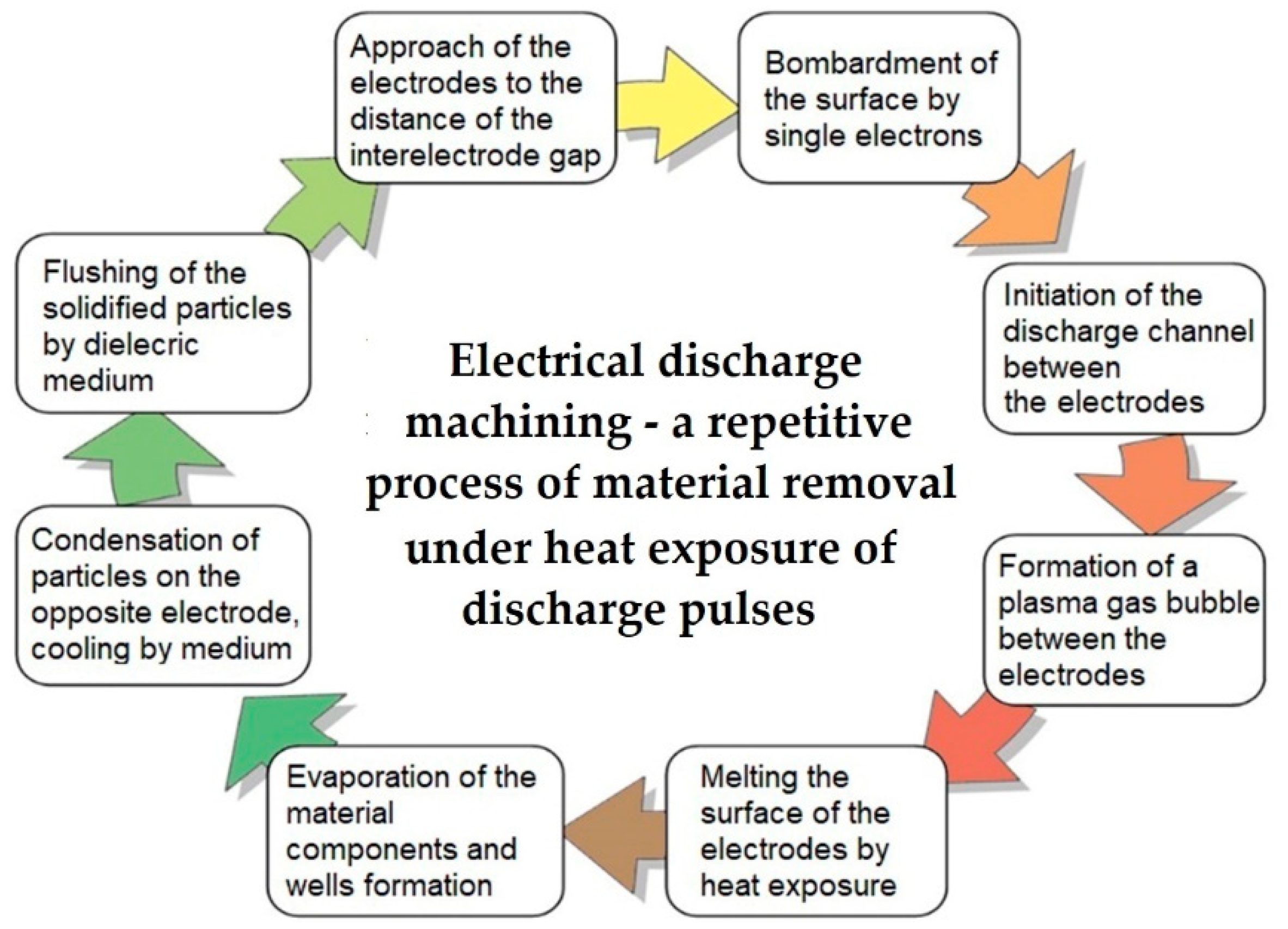
Figure 2.
A schematic cycle of the material erosion under discharge pulses.

Figure 3.
The main factors of EDM affecting the functionality of the final product.


Figure 5.
Schematic diagram of the EDM of non-conductive materials using a specially developed electrically conductive coating: (a) Initiating discharge impulses between the coating and the tool electrode; (b) electrical erosion of the coating, formation of the erosion products between the conductive film and the electrode tool; (c) electrical erosion of the non-conductive workpiece with absorbed erosion products by the workpiece; (d) reinitiating electrical erosion of the workpiece that keeps constant presences of the erosion product in sub layer of the workpiece.

© 2019 by the authors. Licensee MDPI, Basel, Switzerland. This article is an open access article distributed under the terms and conditions of the Creative Commons Attribution (CC BY) license (http://creativecommons.org/licenses/by/4.0/).
Share and Cite
MDPI and ACS Style
Volosova, M.; Okunkova, A.; Peretyagin, P.; Melnik, Y.A.; Kapustina, N. On Electrical Discharge Machining of Non-Conductive Ceramics: A Review. Technologies 2019, 7, 55. https://0-doi-org.brum.beds.ac.uk/10.3390/technologies7030055
AMA Style
Volosova M, Okunkova A, Peretyagin P, Melnik YA, Kapustina N. On Electrical Discharge Machining of Non-Conductive Ceramics: A Review. Technologies. 2019; 7(3):55. https://0-doi-org.brum.beds.ac.uk/10.3390/technologies7030055
Chicago/Turabian StyleVolosova, Marina, Anna Okunkova, Pavel Peretyagin, Yury A. Melnik, and Natalya Kapustina. 2019. "On Electrical Discharge Machining of Non-Conductive Ceramics: A Review" Technologies 7, no. 3: 55. https://0-doi-org.brum.beds.ac.uk/10.3390/technologies7030055
Note that from the first issue of 2016, this journal uses article numbers instead of page numbers. See further details here.