Article

Application-Specific SoC Design Using Core Mapping to 3D Mesh NoCs with Nonlinear Area Optimization and Simulated Annealing

1
Institut für Informations- und Kommunikationstechnik, Otto-von-Guericke-Universität Magdeburg, 39106 Magdeburg, Germany
2
Institute of Electrodynamics and Microelectronics, University of Bremen, 28359 Bremen, Germany
*
Author to whom correspondence should be addressed.
Submission received: 26 November 2019 / Revised: 10 January 2020 / Accepted: 21 January 2020 / Published: 23 January 2020
(This article belongs to the Special Issue MOCAST 2019: Modern Circuits and Systems Technologies on Electronics)

Abstract

:
Core mapping, in which a core graph is mapped to a network graph to minimize communication, is a common design problem for Systems-on-Chip interconnected by a Network-on-Chip. In conventional multiprocessors, this mapping is area-agnostic as the cores in the core graph are uniform and therefore iso-area. This changes for Systems-on-Chip because tasks are mapped to specific blocks and not general-purpose cores. Thus, the area of these specific cores is varying. This requires novel mapping methods. In this paper, we propose a an area-aware cost function for simulated annealing; Furthermore, we advocate the use of nonlinear models as the area is nonlinear: A semi-definite program (SDP) can be used as it is sufficiently fast and shows 20% better area than conventional linear models. Our cost function allows for up to 16.4% better area, 2% better communication (bandwidth times hop distance) and 13.8% better total bandwidth in the network in comparison to the standard approach that accounts for both the network communication and uses cores with varying areas as well.

1. Introduction

Core mapping is one important design-time optimization problem for chips interconnected by Network-on-Chips (NoCs). The target of this mapping problem is a better distribution of work among the cores to improve data movement between them. Different objectives can be found in the literature such as reducing power [1] or avoiding bandwidth limitations [2]. In this paper, the objective optimizes the area of the chip, which is not commonly found in the literature so far because of the tacit assumption of iso-area cores. However, this is not valid for all systems, as specific blocks will have different areas in contrast to general-purpose cores. We extend our work from [3], in which we proposed a nonlinear model to improve area, by incorporating this model in a simulated annealing cost function to solve area-aware core mapping.
The problem of core mapping is defined as follows: The application’s data streams are modeled using a core graph, in which nodes represent cores and edges with their edge weight model the bandwidth of data stream between the cores. This core graph is mapped to a chip, typically a multiprocessor interconnected by an NoC. The chip is represented by a network graph, in which nodes model tiles that reserve space for an NoC router and a core, and edges model links between tiles. The objective of this optimization is minimization of network latency, typically measured in the cumulative hop distance × bandwidth (e.g., [2]), maximization of the throughput, typically measured by the maximum bandwidth transmitted through single links (e.g., [4]), minimization of energy consumption, measured in dynamic router activity (e.g., [1]) or minimization of execution time, measured by the hop distance along the critical path (e.g., [5]). Core mapping is a very common electronic design automation (EDA) task in NoC design and many approaches from exact analytical solutions, e.g., [5], to heuristics such as simulated annealing (SA), e.g., [2], have been proposed.
Recently, Systems-on-Chip (SoCs) gained attention. There are two important differences to multicore processors: First, the function and thus the area of cores varies in SoCs. Thus, the underlying assumption of iso-area cores, which lead to disregarding the core area during core mapping, is not valid anymore. Second, many SoCs such as vision chips [6] are application specific, while multiprocessors are not. Thus, the application properties must be accounted for already during core placement to exploit additional optimization potential. Using conventional approaches, each tile would have to reserve area for the largest core, which is inefficient, naturally. An example is depicted in Figure 1, in which cores of different sizes (orange) allocate less area than reserved (light gray). Therefore, novel approaches are required.
Ref. [3] introduced nonlinear models and compared them against linear models to optimize area during core mapping. Here, we extend this work by proposing a cost function for simulated annealing to optimize the core mapping and the chip area; Specifically, the nonlinear models are used to optimize area within the simulated annealing. Since these nonlinear models are exact for area, we propose a mixed-exact-approximate method to minimize communication and area in SoCs during design-time core mapping.
The remainder of this work is structured as follows: A review of the state-of-the-art is given in Section 2. Next, the area-aware simulated annealing is introduced in Section 3 that uses linear or nonlinear models to optimize area. Both of these models are introduced in Section 4, which are based on our preliminary paper [3] that this work extends. The results obtained with the simulated annealing are reported in Section 5. The work is concluded in Section 6.

2. Related Work

As already explained, many works on core mapping exist. In general, there are two classes of mapping methods: Exact approaches using an analytical model such as a mixed-integer linear program (MILP), an extensive search of the solution space or heuristic approaches that approximate the solution at better runtime, e.g., simulated annealing or particle swarm optimization. Within each class, the approaches can be further classified by their objective functions that e.g., minimize power or maximize performance.
In the first class of exact approaches, the vast majority of works use mixed integer linear programming to solve core mapping: Ref. [7] allows for connecting multiple cores to a single router. By that, energy consumption is minimized by up to 81.2% compared to one-to-one connections. Ref. [8] optimizes mapping and topology selection to minimize bandwidth, area and network component savings by a minimum of 50% each in comparison to traditional design approaches. Ref. [9] maximizes the worst case throughput and also accounts for multi-threaded processes, i.e., mapping of multiple cores to a single tile in the network graph. Ref. [10] minimizes communication energy using mapping; it targets integration into frameworks that find optimal network voltage and frequency. In particular, Ref. [2] is worth mentioning as it is the standard work core mapping in that cores have different areas. The work uses MILP to synthesize an NoC topology from a core graph with area and power annotations. In contrast to this paper, area reduction is not objective. Rather, Ref. [2] reduces power. Different multimedia benchmarks [11] are used for evaluation. This paper is closely related to [2] because of the consideration of area. Thus, we compare against the same benchmarks for a fair comparison. As our objective function is different, we are able to achieve better area figures.
In the second class of heuristic approaches, many different algorithms have been explored, e.g., genetic algorithms (GA), in which solutions evolve, particle swarm optimization (PSO), in which agents collaboratively find a good solution, or simulated annealing (SA), in which cooling processes are used as inspiration to find optimal configurations. Ref. [12] uses GA to minimize the overall execution time of the application. More recently, GA is rarely used due to lower runtime than PSO and SA: Ref. [13] optimizes mapping for partially vertically-connected 3D NoCs to make best use of through-silicon via (TSVs). The authors propose both and MILP and a PSO to improve network congestion, but the MILP has too long of a runtime for realistic use cases. SA is one of the most-used EDA methods. It can be used at many abstraction levels, from gate-level [14] to system-level optimization [15]. A reason therefore lies in SA’s compelling performance, as we will show with a comparison against PSO in this work. The performance for SA can be further by combination with different techniques: For example, Ref. [16] shows that SA core mapping combined with cluster analysis allows for up to 30% better runtime at the same quality of results in comparison to off-the-shelf SA. Ref. [17] shows that application of further knowledge about the structure of the objective function allows for up to 66% better average energy consumption in comparison to a blind search. Ref. [18] also focuses on reduction of energy consumption. In this approach, the router allocation is done prior to voltage islanding, thus saving up to 63% power and delay over Sunfloor [1]. Ref. [19] focuses on runtime reductions under thermal constraints, which are specifically challenging in 3D NoCs. In their work, the authors formulate a communication and thermal aware mapping problem and solve it using custom heuristics. They achieve up to 43% better runtime than related works.
To summarize, there are many approaches in the literature on core mapping in NoC-based multiprocessors. Only a small subset accounts for area because most of the works assume homogeneous cores, which is not always valid for heterogeneous scenarios. As area is nonlinear, intrinsically, it is not possible to model it exact through means of linear models. Thus, a novel approach is required as proposed in this work.

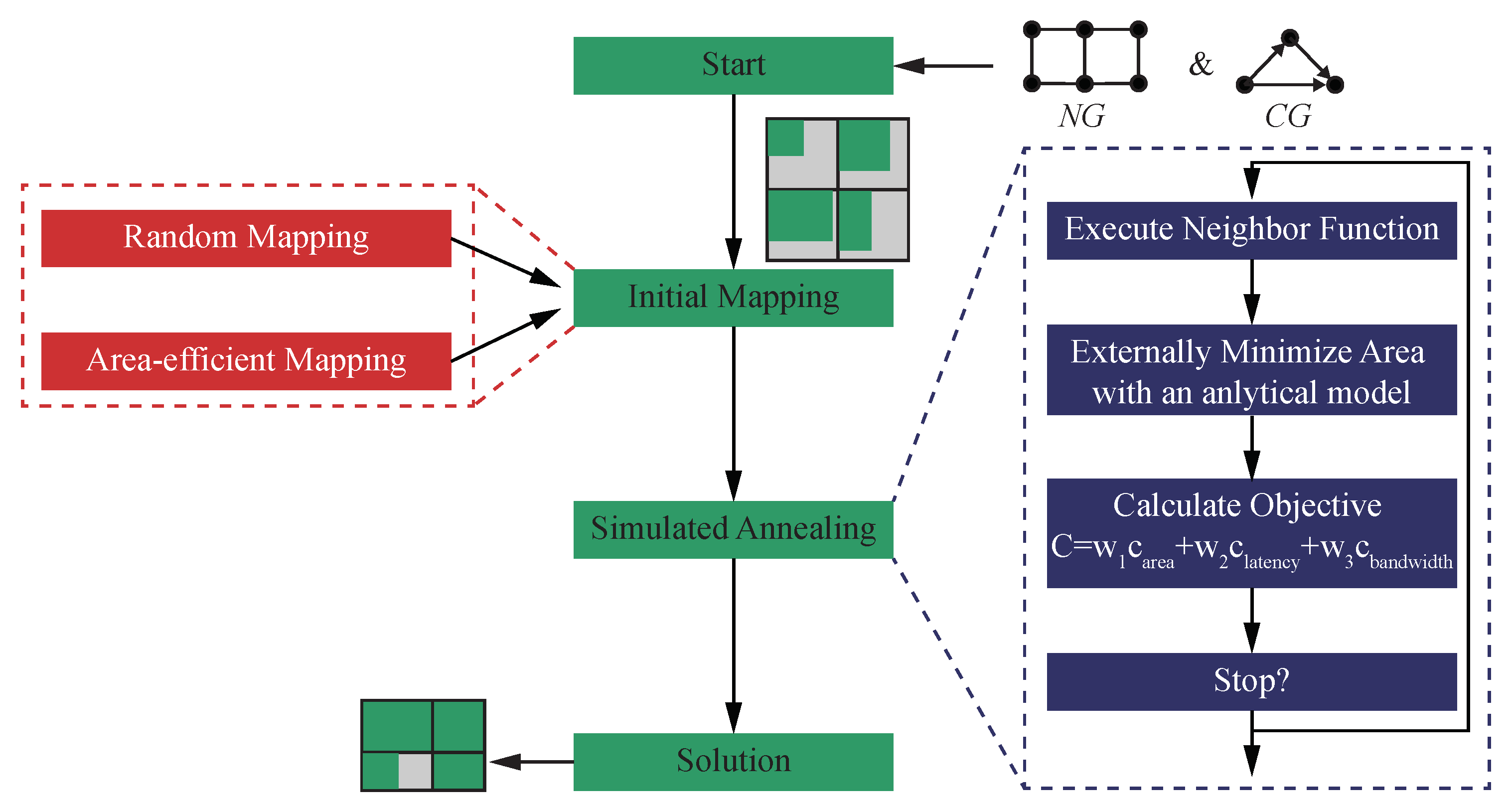
3. Area-Aware Core Mapping with Simulated Annealing

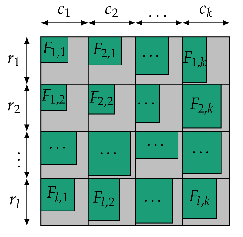
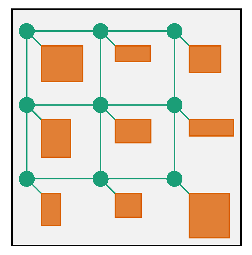
3.1. Problem Definition

The problem of core mapping has been defined multiple times, e.g., [16,20]. The difference to our definition lies in the annotation of the core graph with area. Even more, this area annotation enables the definition of a new objective function including area. The problem of core mapping takes a core graph and a network as input. These are defined as follows:
Definition 1 (Core Graph).
The core graph models the area of cores as well as the bandwidth requirements for communication between cores. It is digraph C G = ( C , E C ) , in which the set C of vertices consists of all cores c i , with i { 1 , , | C | } as the set of core indexes. The set of directed edges e i , j E C models the communication between cores c i and c j C . Cores are area-annotated by the function a r e a : C R + . The bandwidth between nodes is given by the capacity function b a n d w i d t h : E C R + .
Definition 2 (Network Graph).
The network graph models the interconnection topology of the set of target SoC architectures. The network graph is a undirected graph N G = ( T , E T ) , in which the set T of vertices consists of tiles t i , with i { 1 , , | T | } the set of tile indexes, which implement one NoC router each and reserve space for the area of a mapped core. The set of edges e i , j = e j , i E T models the connections between routers in tiles t i and t j T .
The aim of the core mapping is to find a mapping that minimizes an objective function.
Definition 3 (Mapping Function).
The mapping function assigns a core c C to a tile t T . It is defined as
m a p : C T .
The mapping function is injective because each tile can only host one core.
We also define two auxiliary functions. First, the mapping of cores to tiles results in an area requirement for each tile:
Definition 4 (Network Area Function).
The area requirement of each tile is given by the function
F : T R +
that is defined as F ( t j ) = a r e a ( m a p 1 ( t j ) ) . Since the mapping function is injective, m a p 1 is well-defined on the image set of map. Where m a p 1 ( t j ) is not defined, we define F ( t j ) = 0 instead.
Second, we model the flow of packets in the network graph, i.e., the paths of packets based on the routing algorithm, as a source-sink-flow in the network digraph.
Definition 5. 
We define the function f that gives the network flow for each pair of components:
f : E T ( c i , c j ) E C h | h i s a c i c j flow i n N G , value ( h ) = 1 .
The value of the c i - c j -flow is denoted by value(f), following the convention used in [21]. Flows are a very powerful concept, as they give a natural approach to the conversion of core flows to network flows. The function f assigns a flow value to every edge in the network graph E T by considering the flow induced by all edges in the core graph E C . Hence, a flow for a specific pair of cores is assigned to all links in the network, which will be passed by its packets. Consequently, both deterministic and adaptive routing algorithms can be modeled. As packets following deterministic routing algorithms only have one path through the network, the values of the flows will be binary, i.e., the set of links passed by packets has a flow value of 1, while all other links have a flow value of 0. In case of adaptive routing algorithms, the values of the flow along each link will be in the interval of [0,1]. This flow value represents the probability that a packet from the pair of cores will pass this very link when routed.
By that, the objective function of the area-aware core mapping can be defined:
Definition 6 (Objective Function).
O = w 1 O a r e a + w 2 O l a t e n c y + w 3 O b a n d w i d t h .
The heightened addends are defined as follows: The costs for area O a r e a are the total area of the chip including whitespace based in F for a given mapping. The calculation of area is strictly dependent on the network topology. Here, we use a 2D mesh, as shown in Figure 1. The mesh reduces the spacial freedom and requires that cores are located in a grid. Thus, the area of the chip is given by the width W and the height H of the floorplan for this mapping. As the area W H is a product and difficult to calculate in linear models, we use the easy-to-linearize maximum function to approximate area. This results in a model favouring squared chips. The objective for the chip area thus is:
O a r e a = m a x ( W , H ) .
The costs for latency are measured by the hop distance × bandwidth for all data streams in the core graph:
C l a t e n c y = c E C b a n d w i d t h ( c ) | f ( c ) | .
The costs for bandwidth are the maximum bandwidth of any link in the network graph for a given mapping:
O b a n d w i d t h = max v E T c E C b a n d w i d t h ( c ) f ( c ) ( v ) .
This objective function defines the novel problem of area-aware core mapping.

3.2. Simulated Annealing

We solve the area-aware core mapping using simulated annealing. We also implemented an exact solution using an MILP. Since the runtime of this MILP is very poor and only allows for solving input sets with up to seven components in reasonable time, we do not give a detailed definition. Therefore, a heuristic such as a simulated annealing is required. The steps of the simulated annealing are shown in Figure 2. An initial mapping is calculated from a core graph C G and a network graph N G . As depicted, this mapping does not optimize area and therefore includes whitespace (here shown in gray), i.e., unused die area. The initial mapping can either be random or area-efficient, depending on the goals of the optimization. Next, the simulated annealing is executed. The algorithm is initialized with this given valid, but possibly inefficient solution. The solution candidate is modified iteratively by executing the neighbor function that slightly changes the mapping m a p . As a novel feature, we optimize the area analytically within the simulated annealing before calculating the objective function (“Minimize Area” in Figure 2). This allows for a precise area optimization beyond the limitations of heuristics approaches possible by the simulated annealing. We will explain the analytical optimization of area in a separate Section 4. After this analytical step, the complete objective is calculated in that step of the simulated annealing. The algorithm might accept the novel solution based on the value of the objective function. Naturally, the simulated annealing is iterated and stopped when the terminating conditions are met. The final solution returns a mapping function m a p that minimizes area and communication, i.e., includes a floorplan for the given mapping. The initial solution and the neighbor function of the simulated annealing are defined as follows:
Definition 7 (Initial Solution).
There are two ways to generate an initial solution:
  • Randomly generated:The function m a p is generated such that each core c i is assigned to one random tile t j .
  • Area-efficient:The floorplan will be packed area-efficiently, i.e., with minimal whitespace, if all tiles within a row and a column have a similar area. Such a good candidate can be found using a greedy strategy: The cores are sorted descending by area. The tiles are filled from the upper left corner. The cores are assigned to the next free tile in the current row or column, while row and column assignment are alternating. If a row/column is full, tiles will be assigned to the adjacent one. Figuratively speaking, the tiles are filled from the upper left corner to the bottom right corner.
Definition 8 (Neighbor Function).
The neighbor function (or move function) modifies a given mapping function m a p such that it takes the function m a p as input and returns a modified function m a p . Specifically, it is modified by selection a core c i and a tile t j m a p ( c i ) uniform randomly. The selected core is mapped to the selected tile, i.e., position. If a core is already present there, the two mapped cores are swapped. Thus, the modified mapping function m a p is defined as follows:
m a p ( c ) = t j f o r c = c i , m a p ( c i ) f o r m a p 1 ( t j ) i s defined and c = m a p 1 ( t j ) , m a p ( c ) else .
This concludes the definition of the simulated annealing. It remains to optimize the area for a given mapping m a p , as explained in the next section.

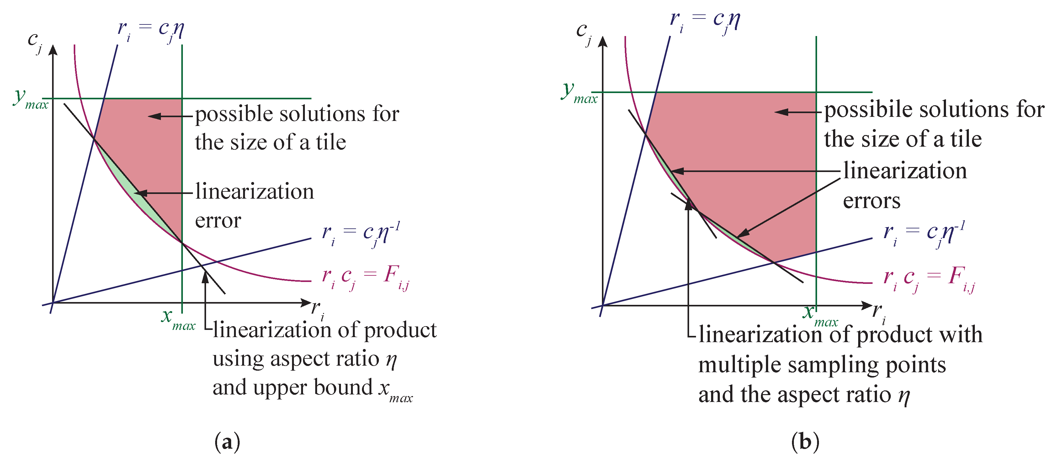
4. Area Optimization for a Given Mapping Using Linear and Nonlinear Models

Conventionally, a mapping of tasks to (multiprocessor) cores would not require an optimization of area since cores are assumed to be identical and thus equal in area. However, this assumption will not be valid in SoCs since each task implements a different IP with varying size. Hence, tasks must also reserve adequate area for their implementing IP. The optimization problem’s constraints and variables are shown in Figure 3: Cores are mapped to a mesh of tiles. Each core has an area value, denoted by F i , j for a core in a given row i and column j. The height of all rows and width of all columns, denoted by c i and r j respectively must be minimized. The multiplication of width and height is constrained by the size of the mapped cores. By that, the white space (gray in Figure 3) is reduced.
More specifically, the area optimization problem during core mapping is formulated as follows [3]: Assume a given mapping of less than or equal of l k cores to tiles in a mesh of l rows and k columns. Each core has the area F i , j , for mapping to row i [ l ] : = { 1 , l } and column j [ k ] : = { 1 , k } . For all empty tiles without a mapped core, F i , j = 0 will be zero. The height of rows is denoted by r i R for all i [ l ] . The width of columns is denoted by c j R for all j [ k ] . The area of each tile is constrained by its mapped core:
r i c j F i , j for all i [ l ] , j [ k ] .
The objective function O 2 minimizes the side length of a square that encloses all tiles (i.e., W = j [ k ] c j , H = i [ l ] r i ):
O 2 = max i [ l ] r i , j [ k ] c j min .
The objective function O 2 is not linear due to the use of the max-function and hence must be linearized. This can be done using an auxiliary variable F ˜ R , which is constrained by the maximum of the summed height and width of the SoC:
F ˜ i [ l ] r i ,
F ˜ j [ k ] c j .
This relatively easy approach is possible because the linearized objective C ˜ function minimizes F ˜ :
O ˜ = F ˜ min .
The issue of modeling Equation (4) remains, which is not linear. We propose both a linear approximation in Section 4.1, which is fast to calculate but does not yield an approximation error, and a nonlinear model in Section 4.2, which is slower than the linear approximation but has no error.

4.1. Linear Model

Since the area of a rectangle F i , j with edge length r i and c j cannot be calculated through means of a linear model, a linear approximation is required. The approach from Lacksonen et al. [22] for the factory layout problem can be applied here as well. Equation (4) is depicted in Figure 4: The iso-area-hyperbola r i c j = F i , j is shown in red in the space of row-heights r i and column-widths c j . Linearization of the iso-area-hyperbola is possible by introduction of an additional constraint for the aspect ratio of each tile. The aspect ratio η ( 0 , 1 ) limits the height and width of tiles for all i [ l ] and j [ k ] : r i c j η and r i c j η 1 . The constraint aspect ratio is shown in Figure 4a in blue.
Figure 4a also shows the solution space as the red-shaded area. Following Equation (4), the area r i c i of a tile i , j must be larger than its core with size F i , j , i.e., F i , j r i c i . The iso-area-hyperbola is the lower left bound for the solution space. The maximum edge length of the tile further limits the solution space, given by the constraints: c j y m a x and r i x m a x . Finally, the solution space is limited by the line equations for the aspect ratios η from Equations (10) and (11).
The iso-area-hyperbola is approximated by a line equation given by the intersections between the lines for the aspect ratios and the maximum edge length. This line equation is shown in black in Figure 4a. The resulting linearization error is plotted in green in Figure 4a. In general, it is possible to reduce this error by using multiple equally-spaced knots as shown in Figure 4b. Each linear equation connecting two adjacent knots intersected with the iso-area-hyperbola ( r i c j = F i , j ) is called a 1-spline. While more 1-splines reduce the error, they also significantly increase the model complexity. Integer inequalities are required to determine in which spline a given solution is located. There are at least three additional integer inequalities per supporting point. Naturally, this reduces runtime performance.
To summarize, the linear optimization minimizes
C ˜ = F ˜ min ,
subject to the following constraints with aspect ratio η ( 0 , 1 ) :
r i η c j i [ l ] , j [ k ] ,
c j η r i i [ l ] , j [ k ] ,
r i + c j F i , j η + F i , j / η i [ l ] , j [ k ] .
Equation (4) is approximated by Equation (12) for one single 1-spline as in Figure 4a. It can easily be deducted from the intersections of the iso-area-hyperbola and Equations (10) and (11). The required values for F i , j η + F i , j / η can be precalculated before starting the optimization and thus are constants within the linear model.

4.2. Nonlinear Model

To remove the linearization error, SDPs can be used because they can express the red iso-area-hyperbola in Figure 4. We set k l variables X k ( i 1 ) + j such that
X k ( i 1 ) + j = r i F i , j F i , j c j 0 , i [ l ] , j [ k ] .
These matrices are premised to be positive semidefinite (i.e., “ 0 ”); thus, each principal minor is greater or equal to 0:
d e t X k ( i 1 ) + j 0 ,
r i c j F i , j 0 ,
r i c j F i , j , i [ l ] , j [ k ] .
We formulate a SDP. The objective function minimizes the linearized variable x max { r i , c i } using Equations (6) and (7):
x = F ˜ min ,
subject to the following constraints.
We assign the corresponding area values to each matrix using the Frobenius inner product:
2 F i j 0 1 1 0 , X k ( i 1 ) + j 2 F i j , i [ l ] , j [ k ] .
For each i [ l ] , the upper left entry of the matrices X k ( i 1 ) + j has the same value for all j [ k ] (this models r i ):
0 1 0 0 0 , X k ( i 1 ) + 1 + 1 0 0 0 , X k ( i 1 ) + j 0 .
For each j [ k ] , the lower right entry of the matrices X k ( i 1 ) + j has the same value for all i [ l ] (this models c j ):
0 0 0 0 1 , X j + 0 0 0 1 , X k ( i 1 ) + j 0 .
We model the maximum variable x for the objective function (this models x r i and x c i ):
0 x + i = 1 l 1 0 0 0 , X k ( i 1 ) + 1 ,
0 x + j = 1 k 0 0 0 1 , X j .
Again, areas of tiles are constrained by an aspect ratio η . Note that this aspect ratio is not violated by the relation between r i and c j . Rather, a component can find a rectangle inside the bounding box given by r i c j . This rectangle has the size of the core. The aspect ratio of its edges is greater than η . We formulate for all i [ l ] and for all j [ k ] :
η F i , j 1 0 0 0 , X k ( i 1 ) + 1 ,
η F i , j 0 0 0 1 , X j .

5. Results

5.1. Simulated Annealing (SA) vs. Particle Swarm Optimization (PSO)

Our approach is compared against [13], which uses PSO to map an application on a partially vertically-connected 3D mesh NoC with cores of different sizes. It is one of the most recent works on mapping in NoCs at the time of writing this paper, and it does account for cores of different areas, but it does not optimize area. To compare against this work, we use our cost function with the SA to map video object plane detection (VOPD) benchmark to a 3D-connected 4 × 2 × 2 NoC and double video object plane detection (DVOPD) benchmark to a 4 × 4 × 2 NoC with a varying number of vertical connections. The benchmark application graphs are from [23]. The other benchmarks from [23] are smaller and thus a comparison is not useful because both the PSO and the proposed heuristic algorithm using a simulated annealing will find the global minimum in a small design space in a short time. We chose an arbitrary but identical initial mapping for both benchmarks and both algorithms. We use 20 reruns for both PSO and simulated annealing so that both the algorithms have approximately the same computation time budget. The parameters of the PSO are given by [13] (k1 = 1, k2 = 0.04, k3 = 0.02). The parameters for the simulated annealing are: initial temperature 30, cooling 0.97, 1000 iterations. Both [13] and the our approach use the same objective function that minimizing bandwidth t i m e s communication hop distance. We disregard area because it is not used in [13] and therefore would skew the comparison. We change the TSV count in the NoCs to vary the mapping difficulty. The results are shown in Table 1 for VOPD and in Table 2 for DVOPD. The proposed heuristic algorithm allows for up to 15% improved performance with 2.564–3.125% better performance in average.

5.2. Linear vs. Non-Linear Model

We compare our linear and nonlinear models by generating results for the same inputs with both the LP and the SDP. We implement our models in MATLAB R2018a and they are available from Github [24]. The LPs use IBM CPLEX 12.8.0 [25] as optimization engine. The SDPs use Mosek 8.1 [26]. We generate three random input benchmarks as in [3]. Iso-area cores are used for a fair comparison against conventional approaches:
  • A 3D SoC with two layers and five tiles, of which three tiles are in layer 1 and two tiles are in layer 2.
  • A 3D SoC with four layers and 10 tiles per layer connected by a 2 × 5 mesh NoC.
  • A 3D SoC with four layers and 20 tiles per layer connected by a 4 × 5 mesh NoC.
Cores are set to be 10 mm2 large. Routers with five ports require 1 mm2. The router area is linearly proportional to port count depending on the position of the router in the network. TSV arrays, which vertically connect routers, are 2 mm2 large. The aspect ratio is limited by η = 0.1 . We run the optimization 50 times to average runtime on an Intel Core i7-6700 (eight cores at 3.4 GHz) using Windows 10.
The results for performance, runtime and model properties are reported in Table 3:
  • Performance. In benchmark 1, the summed chip area is 68.7 mm2 from the LP and 59.8 mm2 from the SDP. In benchmark 2, the summed chip area is 832 mm2 from the LP and 695 mm2 from the SDP. In benchmark 3, the summed chip area is 1272 mm2 from the LP and 1188 mm2 from the SDP. Since in the lowest layer there is no TSV area required (there are no keep-out-zones using via-middle-process-flow), this layer is smaller.
  • Runtime. The difference in runtime between LP and SDP is between 6× and 31%. The LP loses its runtime advantage for larger inputs.
  • Model Properties. We also report inequality and variable count. The linear model requires 2 k l + 2 inequalities and k + l + 1 variables. The nonlinear model requires ( k l ) 2 + k + l + 2 inequalities and k l + 1 variables. Thus, the SDP has considerably more variables and inequalities. However, both models are very small in comparison to common use cases for LP and SDP solvers with millions of variables and equations. Therefore, the models do not largely differentiate in terms of memory usage.

5.3. SA for Area-Aware Core Mapping with Linear vs. Nonlinear Models

As introduced in the related work, Ref. [2] compares against our approach as it conducts core mapping and accounts for varying area of cores. Only quadratic-shaped cores of are mapped to a 2D mesh NoC in that work. The reference’s objective function does not target a low area but minimizes transmission energy. We compare the results from our nonlinear model with results from linear models from [2] using the three multimedia benchmarks provided, which cover video and audio decoder and encoder. The data streams for the benchmarks are taken from [23] and the cores’ area from [2].
The results for area, hop distance × bandwidth and total bandwidth are reported in Table 4. The three figures are measured following Def. 6. For our experiments, we take the mapping from [23] as baseline. Next, we optimize this mapping with the SDP to demonstrate the advantages of nonlinear models at a realistic benchmark. Then, we generate an area-efficient initial solution following the greedy algorithm introduced in Section 3.2. Then, we conduct two separate experiments with our SA cost function. First, we set the weight for area in our cost function (Equation (2)) w 1 to zero, so that only communication is minimized. This resembles the behavior of the objective function in [2]. Second, the weights in the objective function (Equation (2)) are normalized such that area and communication are accounted for simultaneously. The simulated annealing is executed 20 times with 15,000 iterations, an initial temperature of 30 and a cooling of 0.98. The aspect ratio is limited by η = 0 . 1 in both these experiments. The results of all runs are averaged and the standard deviation is calculated. A single run of the SA terminates after 17 minutes on a Windows 10 workstation using an Intel i7-7740X processor (8 cores at 4.3 GHz).
In the first experiment, the heuristic from [2] and the proposed cost function with SA produce similar results: hop distance × bandwidth with between 5% better and 3% worse, while total bandwidth shows more variation with 14% better to 24% worse. Since we do not optimize area, the results are purely by chance. For the second experiment, our proposed algorithm shows the following improvement: In the best case, the H263 enc mp3 dec, the proposed cost function for a simulated annealing improves area by 16.4%, hop distance × bandwidth by 2% and total bandwidth by 13.8%. Both experiments show that the quality of results depends on the structure of the input data. While the H263 enc mp3 dec benchmark offers large optimization potential, the mp3 enc mp3 dec benchmark shows minor differences in area and hop distance × bandwidth. The H256 dec mp3 dec benchmark offers the large area improvement by 27%. However, this comes at a price of higher communication costs by up to 9.66%.

6. Conclusions

To summarize our paper, we showed a cost function for a simulated annealing algorithm to optimize area and communication during core mapping for NoC-based SoCs. As a novel feature, the heuristic is area-aware, which is a new requirement from heterogeneous core and IP areas in modern SoCs. We conducted experiments to compare the proposed algorithm against the state-of-the-art in the subject areas. First, we justify the use of simulated annealing over other heuristic searches by comparison against a recent work on core mapping using PSO. SA performs 2.5–3% better on average for different benchmarks with the same computational time budget. Second, we compare linear with nonlinear models to optimize area within the simulated annealing. We find that the nonlinear SDP yields 12.5–17.3% reduced area for different randomly generated inputs, which is within the expectations for the chosen linearization (Ref. [22] reports 20% area error for similar problems). In addition, as expected, the runtime of the SDP is longer than of a linear model. However, even for the largest example, the SDP only runs 3.6 seconds longer absolutely. This is a rather small price to pay for 17.3% better area. Third, our cost function is compared against the state-of-the-art mapping including area. For a H263 enc mp3 dec benchmark, our approach generates 16.4% better area, 2% better hop distance × bandwidth and 13.8% better total bandwidth. These three experimental setups show that our approach is practical, as it reduces area and communication costs for real-world based benchmarks, efficient, as it has runtime as state-of-the-art, and effective, as it allows for reduced area by elimination of linearization errors. By that, we demonstrate the practical applicability of nonlinear models in EDA.

Author Contributions

Data curation, D.E.; Project administration, T.P.; Supervision, A.G.-O.; Validation, L.B.; Writing—original draft, J.M.J. All authors have read and agreed to the published version of the manuscript.

Funding

This research was funded by the German Research Foundation (DFG) project PI 447/8 and GA 763/7. This work was supported by a fellowship within the Internationale Forschungsaufenthalte für Informatikerinnen und Informatiker (IFI) programme of the German Academic Exchange Service (DAAD).

Conflicts of Interest

The authors declare no conflict of interest. The funders had no role in the design of the study; in the collection, analyses, or interpretation of data; in the writing of the manuscript, or in the decision to publish the results’.

References

  1. Murali, S.; Coenen, M.; Radulescu, A.; Goossens, K.; De Micheli, G. A Methodology for Mapping Multiple Use-Cases onto Networks on Chips. In Proceedings of the Conference on Design, Automation and Test in Europe, Munich, Germany, 6–10 March 2006. [Google Scholar] [CrossRef] [Green Version]
  2. Srinivasan, K.; Chatha, K.S.; Konjevod, G. Linear-programming-based techniques for synthesis of network-on-chip architectures. IEEE Trans. Very Large Scale Integr. (VLSI) Syst. 2006, 14, 407–420. [Google Scholar] [CrossRef]
  3. Joseph, J.M.; Ermel, D.; Drewes, T.; Bamberg, L.; García-Oritz, A.; Pionteck, T. Area Optimization with Non-Linear Models in Core Mapping for System-on-Chips. In Proceedings of the 8th International Conference on Modern Circuits and Systems Technologies (MOCAST), Thessaloniki, Greece, 13–15 May 2019. [Google Scholar] [CrossRef]
  4. Lin, L.-Y.; Wang, C.-Y.; Huang, P.-J.; Chou, C.-C.; Jou, J.-Y. Communication-driven task binding for multiprocessor with latency insensitive network-on-chip. In Proceedings of the Asia and South Pacific Design Automation Conference (ASP-DAC), Shanghai, China, 21–21 January 2005. [Google Scholar] [CrossRef]
  5. Satish, N.; Ravindran, K.; Keutzer, K. A Decomposition-based Constraint Optimization Approach for Statically Scheduling Task Graphs with Communication Delays to Multiprocessors. In Proceedings of the Conference on Design, Automation and Test in Europe, Nice, France, 16–20 April 2007. [Google Scholar]
  6. Zarándy, Á. Focal-Plane Sensor-Processor Chips; Springer: Berlin, Germany, 2011. [Google Scholar]
  7. Rhee, C.-E.; Jeong, H.-Y.; Ha, S. Many-to-many core-switch mapping in 2-D mesh NoC architectures. In Proceedings of the IEEE International Conference on Computer Design (ICCD): VLSI in Computers and Processors, San Jose, CA, USA, 11–13 October 2004. [Google Scholar] [CrossRef]
  8. Murali, S.; Benini, L.; De Micheli, G.; De Micheli, G.; De Micheli, G. Mapping and Physical Planning of Networks-on-chip Architectures with Quality-of-service Guarantees. In Proceedings of the 2005 Asia and South Pacific Design Automation Conference, Shanghai, China, 18–21 January 2005. [Google Scholar] [CrossRef] [Green Version]
  9. Ostler, C.; Chatha, K.S. An ILP Formulation for System-level Application Mapping on Network Processor Architectures. In Proceedings of the Conference on Design, Automation and Test in Europe, Nice, France, 16–20 April 2007. [Google Scholar]
  10. Ozturk, O.; Kandemir, M.; Son, S.W. An ilp based approach to reducing energy consumption in nocbased CMPS. In Proceedings of the 2007 international symposium on Low power electronics and design (ISLPED), Portland, OR, USA, 27–29 August 2007. [Google Scholar] [CrossRef]
  11. Hu, J.; Marculescu, R. Energy-aware mapping for tile-based NoC architectures under performance constraints. In Proceedings of the 2003 Asia and South Pacific Design Automation Conference, Kitakyushu, Japan, 21–24 January 2003. [Google Scholar]
  12. Lei, T.; Kumar, S. A two-step genetic algorithm for mapping task graphs to a network on chip architecture. In Proceedings of the Euromicro Symposium on Digital System Design, Belek-Antalya, Turkey, 1–6 September 2003. [Google Scholar] [CrossRef] [Green Version]
  13. Manna, K.; Swami, S.; Chattopadhyay, S.; Sengupta, I. Integrated Through-Silicon Via Placement and Application Mapping for 3D Mesh-Based NoC Design. ACM Trans. Embedded Comput. Syst. 2016, 16. [Google Scholar] [CrossRef]
  14. Cong, J.; Wei, J.; Zhang, Y. A thermal-driven floorplanning algorithm for 3D ICs. In Proceedings of the IEEE/ACM International Conference on Computer Aided Design (ICCAD), San Jose, CA, USA, 7–11 November 2004. [Google Scholar] [CrossRef] [Green Version]
  15. Joseph, J.M.; Ermel, D.; Bamberg, L.; García-Ortiz, A.; Pionteck, T. System-level optimization of Network-on-Chips for heterogeneous 3D System-on-Chips. arXiv 2019, arXiv:cs.AR/1909.13807. [Google Scholar]
  16. Lu, Z.; Xia, L.; Jantsch, A. Cluster-based Simulated Annealing for Mapping Cores onto 2D Mesh Networks on Chip. In Proceedings of the 11th IEEE Workshop on Design and Diagnostics of Electronic Circuits and Systems, Bratislava, Slovakia, 16–18 April 2008. [Google Scholar] [CrossRef]
  17. Zhong, L.; Sheng, J.; Jing, M.; Yu, Z.; Zeng, X.; Zhou, D. An optimized mapping algorithm based on Simulated Annealing for regular NoC architecture. In Proceedings of the 9th IEEE International Conference on ASIC, Xiamen, China, 25–28 October 2011. [Google Scholar] [CrossRef]
  18. Kashi, S.; Patooghy, A.; Rahmatiy, D.; Fazeli, M.; Kinsy, M.A. Application Specific Networks-on-Chip Synthesis: An Energy Efficient Approach. In Proceedings of the 2018 IEEE Computer Society Annual Symposium on VLSI (ISVLSI), Hong Kong, China, 8–11 July 2018. [Google Scholar] [CrossRef]
  19. Li, B.; Wang, X.; Singh, A.K.; Mak, T. On runtime communication- and thermal-aware application mapping in 3D NoC. In Proceedings of the 11th IEEE/ACM International Symposium on Networks-on-Chip (NOCS), Seoul, Korea, 19–20 October 2017. [Google Scholar]
  20. Murali, S.; Micheli, G.D. Bandwidth-constrained mapping of cores onto NoC architectures. In Proceedings of the Design, Automation and Test in Europe Conference and Exhibition, Paris, France, 16–20 February 2004. [Google Scholar] [CrossRef] [Green Version]
  21. Korte, B.; Vygen, J. Combinatorial Optimization: Theory and Algorithms, 5th ed.; Springer: Berlin, Germany, 2012. [Google Scholar]
  22. Lacksonen, T.A. Static and Dynamic Layout Problems with Varying Areas. J. Oper. Res. Soc. 1994, 45, 59–69. [Google Scholar] [CrossRef]
  23. Sahu, P.K.; Chattopadhyay, S. A survey on application mapping strategies for Network-on-Chip design. J. Syst. Archit. 2013, 59, 60–76. [Google Scholar] [CrossRef]
  24. Joseph, J. System-Level Optimization of NoCs for Hetergeneous 3D SoCs. 2019. Available online: https://github.com/jmjos/A-3D-NoC-DSE (accessed on 8 October 2019).
  25. IBM. ILOG CPLEX Optimization Studio CPLEX User’s Manual 12.8; Armonk: New York, NY, USA, 2017. [Google Scholar]
  26. Mosek ApS. Mosek User Manual; Mosek ApS: Kopenhagen, Denmark, 2018. [Google Scholar]
Figure 1. Cores (orange) of different areas on an SoC, attached to a 2D-mesh NoC [3].
Technologies 08 00010 g001
Figure 2. Simulated annealing algorithm.
Technologies 08 00010 g002
Figure 3. Variables and constraints of area optimization.
Technologies 08 00010 g003
Figure 4. Area linearization [3]. (a) Simple approximation with single linear equation. (b) Reduced error through multiple linear approximations.
Technologies 08 00010 g004
Table 1. Comparison of simulated annealing (SA) vs. particle swarm optimization (PSO) from [13] for VOPD benchmark. Network performance comparison (hop distance [HD] × bandwidth [Mb]). Twenty reruns for PSO and simulated annealing with the same computational time budget for different TSV counts.
Vertical Connection CountHop Distance × Bandwidth [Hd Mb]Difference
PSOProposed
meanstdmeanstd
112,229012,22900%
210,5915819005015%
38894102865903%
49013364859505%
58725155859501%
68723148859501%
785950859500%
885950859500%
Average Improvement3.125%
Table 2. Comparison of SA vs. PSO from [13] for DVOPD benchmarks. Network performance comparison (hop distance [HD] × bandwidth [Mb]). Twenty reruns for PSO and simulated annealing with the same computational time budget.
Vertical Connection CountHop Distance × Bandwidth [Hd Mb]Difference
PSOProposed
meanstdmeanstd
143,330043,33000%
238,27416337,9543951%
334,636033,85402%
434,21767432,38205%
533,24955531,01407%
632,35169930,16807%
731,92057529,91606%
830,76767929,74403%
930,76767929,74403%
1030,31845329,71202%
1130,23540929,71202%
1229,7646929,71200%
1329,99634029,71201%
1429,80520829,71200%
1529,712029,71200%
1629,712029,71200%
Average Improvement2.563%
Table 3. Area, runtime, inequality count and variable count comparison between linear and nonlinear model (runtime average of 50 reruns) [3].
LayerArea [mm2]
5 PEs40 PEs80 PEs
LPSDPΔLPSDPΔLPSDPΔ
143.036.8−14.4%211178−15.6%364301−17.4%
225.723.0−10.5%222180−18.9%379313−17.4%
3214183−14.5%378313−17.2%
4185154−16.8%316261−17.4%
Average AreaReduction −12.5% −16.5% −17.3%
Average runtime [s]
0.42.9+625%3.97.5+92.3%12.216.0+31.1%
Inequality count
1631+94%88436+395%1681644+879%
Variable count
921+133%32112+250%40200+400%
Table 4. Area and network performance comparison of mapping to a 2D-mesh NoC using the simulated annealing (SA) from [2]. The SA is executed with 20 reruns, an initial temperature of 30, cooling of 0.98 and 15,000 iterations. The aspect ratio is limited by η = 0 . 1 [3].
Area [mm2]Hop Distance × BandwidthBandwidth [Bits]
meanstdRatiomeanstdRatiomeanstdRatio
H256 decmp3 decBaseline [2]11,30119,8584060
Baseline with SDP10,178−9.94%19,8580.0%40600.0%
Initial solution7902−30.1%33,707+69.7%7994+96.9%
SA communication ( w 1 = 0 )11,6991598+3.52%20,449404+2.98%4265201+5.05%
Normalized SA with SDP8244505−27.1%21,280624+7.16%4452674+9.66%
H263 encmp3 decBaseline [2]12,535255,32484,884
Baseline with SDP10,178−18.8%255,3240.0%84,8840.0%
Initial solution6993−44.2%525,537+106%85,244+0.42%
SA communication ( w 1 = 0 )15,7621723−25.7%241,47915,333−5.42%73,01214,302−14.0%
Normalized SA with SDP10,4742148−16.4%250,18714,763−2.0%73,16117,497−13.8%
mp3 encmp3 decBaseline [2]8568175464085
Baseline with SDP8091−5.57%17,5460.0%40850.0%
Initial solution7281−15.0%39,171+123.3%6560+60.1%
SA communication ( w 1 = 0 )10,7791460+25.8%17,341342−1.17%5065906+24.0%
Normalized SA with SDP8516796−0.61%17,572487+0.15%4974902+21.8%

