A New Simplified Model and Parameter Estimations for a HfO2-Based Memristor †


Department Theoretical Electrical Engineering, Technical University of Sofia, 1000 Sofia, Bulgaria
†
This paper is an extended version of the paper published in 8th International Conference on Modern Circuit and System Technologies on Electronics and Communications (MOCAST 2019), Thessaloniki, Greece, 13–15 May 2019.
Technologies 2020, 8(1), 16; https://doi.org/10.3390/technologies8010016
Submission received: 30 January 2020
/
Revised: 28 February 2020
/
Accepted: 3 March 2020
/
Published: 7 March 2020
(This article belongs to the Special Issue MOCAST 2019: Modern Circuits and Systems Technologies on Electronics)
Abstract
:The purpose of this paper was to propose a complete analysis and parameter estimations of a new simplified and highly nonlinear hafnium dioxide memristor model that is appropriate for high-frequency signals. For the simulations; a nonlinear window function previously offered by the author together with a highly nonlinear memristor model was used. This model was tuned according to an experimentally recorded current–voltage relationship of a HfO2 memristor. This study offered an estimation of the optimal model parameters using a least squares algorithm in SIMULINK and a methodology for adjusting the model by varying its parameters overbroad ranges. The optimal values of the memristor model parameters were obtained after minimizing the error between the experimental and simulated current–voltage characteristics. A comparison of the obtained errors between the simulated and experimental current–voltage relationships was made. The error derived by the optimization algorithm was a little bit lower than that obtained by the used methodology. To avoid convergence problems; the step function in the considered model was replaced by a differentiable tangent hyperbolic function. A PSpice library model of the HfO2 memristor based on its mathematical model was created. The considered model was successfully applied and tested in a multilayer memristor neural network with bridge memristor–resistor synapses
1. Introduction
The memristor is a very important electricone-port element, together with the capacitor, resistor, and inductor [1,2]. It is a passive electronic component. The memristor is a highly nonlinear electronic element with many possible applications in reconfigurable analogue and digital devices, nonvolatile memories, neural networks, and many others [1,2,3]. It relates the electric charge q, described as a time integral of the current, and the flux linkage Ψ, expressed as a time integral of the memristor voltage v [1,2]. The idealized memristor was forecasted by L. Chua in 1971 [1], in agreement withsymmetry considerations and the relationships between the main electrical variables (voltage v, current i, electric charge q, and magnetic flux linkage Ψ). Its current–voltage characteristic is a pinched hysteresis loop and the respective charge–flux relationship is a monotonically increasing nonlinear curve. The memristor has a salient and very beneficial property, namely retaining its state (and the respective resistance) after turning the electric sources off [2,4]. Several basic material realizations of memristors exist in the scientific literature, such as those made using transition metal oxides, polymeric materials, ferroelectric structures, and others. The memristor realizations usingHfO2 or other perspective amorphous metal-oxide materials [2,4] have physical sizes in the nanoscale range. Its energy consumption is several times lower than that of conventional microelectronic components [4,5]. The first physical memristor prototype based on titanium dioxide was created in Hewlett Packard’s scientific laboratories by Stanley Williams’ research team in 2008 [2,4]. Many scientific papers on memristors and memristor-based circuits have been published and several corresponding memristor models have been offered [6,7,8,9,10]. The linear ionic drift memristor model [2] is applied for low-level voltage signals. The nonlinear ionic drift models proposed by Biolek [4] and Joglekar [3] are capable of expressing the memristor nonlinear behavior for high-level voltage signals according to the memristor state variable x. The highly nonlinear Lehtonen–Laihomemristor model [7,8] is based on physical measurements and on the mechanism of the electric current flow through amorphous semiconducting transition-metal oxides [8]. It has a good precision, is adjustable, and can be described using mathematical equations [7,8]. This memristor model was applied after a tuning procedure according to the experimental current–voltage relationships of an HfO2 memristor element [10] in the present investigation [7,8]. The main interest in the present case is associated with new and not very well analyzed types of memristors, such as transition-metal oxide memristors, especially hafnium oxide memristors [10,11,12]. Several basic models of HfO2-based memristors exist in the technical literature [10,11,12,13]. To the best of the author’s knowledge, some of them are either very complex [10] or not sufficiently precise [11]. Other models, such as Biolek’s [4] and Joglekar’s [3], are not able to correctly express the corresponding i–v relationship due to the low nonlinearity of the current–voltage characteristic. The motivation for the present investigation was to offer a simple nonlinear ionic drift model for a HfO2memristor with a strongly nonlinear window function [14,15],parameter estimations of the model using the least squares algorithm in MATLAB-Simulink [15,16], to minimize the root mean square error and provide a simulation the memristor model with the obtained parameters, to compare the derived errors with those obtained using the applied methodology, to compare the errors with those derived using the best existing memristor models [10,11], and to replace the step function in the considered model using a differentiable tangent hyperbolic function [17]. For this aim, the tunable modified nonlinear memristor model proposed in References [7,8] is very suitable, in combination with the highly nonlinear window function, offered by Mladenov and Kirilov [14]. After tuning the considered model according to the experimental current–voltage characteristics of a HfO2 memristor [10] in MATLAB-Simulink [18], a PSpice library memristor modelwas created using the proposed mathematical model; then, it was analyzed in OrCAD PSpice [15,19]. The considered memristor model was tested in a simple multilayer neural network for function fitting [20] with bridge resistor–memristor synapses [21,22,23]. The capability of the used memristor model [7,8,14] for operation in complex circuits was confirmed.
The paper is organized as follows: A description of the memristor model considered in this research is presented in Section 2. Its adjustment to the experimental data and parameters estimation are presented in Section 3. The analysis of the respective PSpice memristor library model in the OrCAD PSpice environment is given in Section 4. The application of the considered memristor model in a simple memristor-based multilayer neural network is described in Section 5. The concluding remarks are given in Section 6.
2. A Description of the Proposed Hafnium Dioxide Memristor Model
The considered memristor element is based on HfO2material [9,10]. In References [7,8], a model based on physical measurements for transition metal oxide memristors is presented. It is founded on experimentally recorded current–voltage characteristics [10]. This model was applied for the description of the considered HfO2-based memristor. The approximated current–voltage relationship [6,7] is expressed using Equation (1):
where α = 1.65 V−1, β = 100 µA, γ = 0.008 V−1, and χ = 1500 µA are the adjusting parameters, and n = 5 is a parameter that describes the influence of the memristor state variable x on the current. The first term in Equation (1) describes the rectifying properties of the memristor for high-level signals. The second term includes a hyperbolic sine term and represents the memorizing effect of the memristor element. The parameters β and χ are used for the expression of both symmetric and non-symmetric current–voltage characteristics. The parameter α determines the area of the current–voltage pinched hysteresis loop. The coefficient γ represents the exponentially increasing nonlinear ionic dopant drift for higher voltage signals.
In this memristor model described in References [7,8], the state variable x is a normalized parameter in the range [0,1]. This memristor model illustrates an asymmetric switching behavior. When the memristor is in a highly conductive ON state, the state variable is near unity and the electric current is dominated by the second term in Equation (1), which represents a tunneling effect [7,8]. If the memristor element is in a low conductive OFF state, the state variable x is close to zero and the current is primarily represented by the first term in Equation (1), which represents a diode equation [7,8]. The considered memristor model [7,8] uses a nonlinear relation between the time derivative of the state variable x and the voltage v in the state differential equation [7,8] in accordance with Equation (2):
where a = 0.9 is a constant adjusting parameter, s = 5 is an odd integer exponent, and f(x) is a window function used for the approximate illustration of the nonlinear ionic dopant drift and the specific boundary effects for the hard-switching mode [3,4,14,23]. If the state variable does not reach its limiting values, namely zero and unity the memristor operations in a soft-switching mode, then the pinched hysteresis loop of the current–voltage characteristic is a symmetric curve around the origin. When the state variable reaches its limiting values, then the memristor operates in a hard-switching mode. If the state variable is equal to unity, then the boundary between the doped and the undoped regions of the memristor coincides with the cathode of the element. If the voltage increases, then the state variable remains equal to unity and cannot increase due to physical limitations. When the voltage changes its direction, the state variable immediately decreases. When the state variable is equal to zero, then the boundary between the doped and the undoped regions coincides with the anode. If the voltage decreases, then the state variable remains equal to zero and cannot decrease due to physical restrictions. If the voltage changes its direction, then the state variable immediately increases. If the memristor operates in a hard-switching mode, then it behaves as a rectifying diode [23]. Its current–voltage relationship is a non-symmetrical one.
The applied window function adds nonlinearity to the model according to the state variable x of the memristor element [14]. Equations (1) and (2) fully define the corresponding applied physics-based memristor model [7,8]. The ionic transport is linked to the ionic dopant drift and the electron motion in the respective hafnium dioxide material [10,11,12]. The applied window function is a modification of the standard Biolek window function [4]:
and it is described in detail in Mladenov and Kirilov [14]. The step function stp is expressed as follows [4]:
This step function is a non-differentiable one, and if it is directly applied in the corresponding PSpice memristor library model, sometimes convergence problems are expected [17]. To avoid such problems in the present research, the step function stp is replaced by its differentiable analogue:
where the coefficient r determines the steepness of the considered function, whereits value is between 30 and 70. The modified window function is:
This window function could be also described using Equation (7):
where m = 0.23 is a tuning coefficient describing the domination of the introduced sinusoidal component, p is a positive integer exponent, fBM is the modified Biolek window function [14], and vthr is the activation threshold of the memristor [23]. If the absolute value of the applied voltage v is lower than the activation threshold vthr, then the memristor state variable does not change and the memristance is a constant. If the voltage is higher than the activation threshold, then the memristor has a memorizing effect. The applied modified memristor model is based on Equations (1), (2), and (7), and it is described using Equation (8):
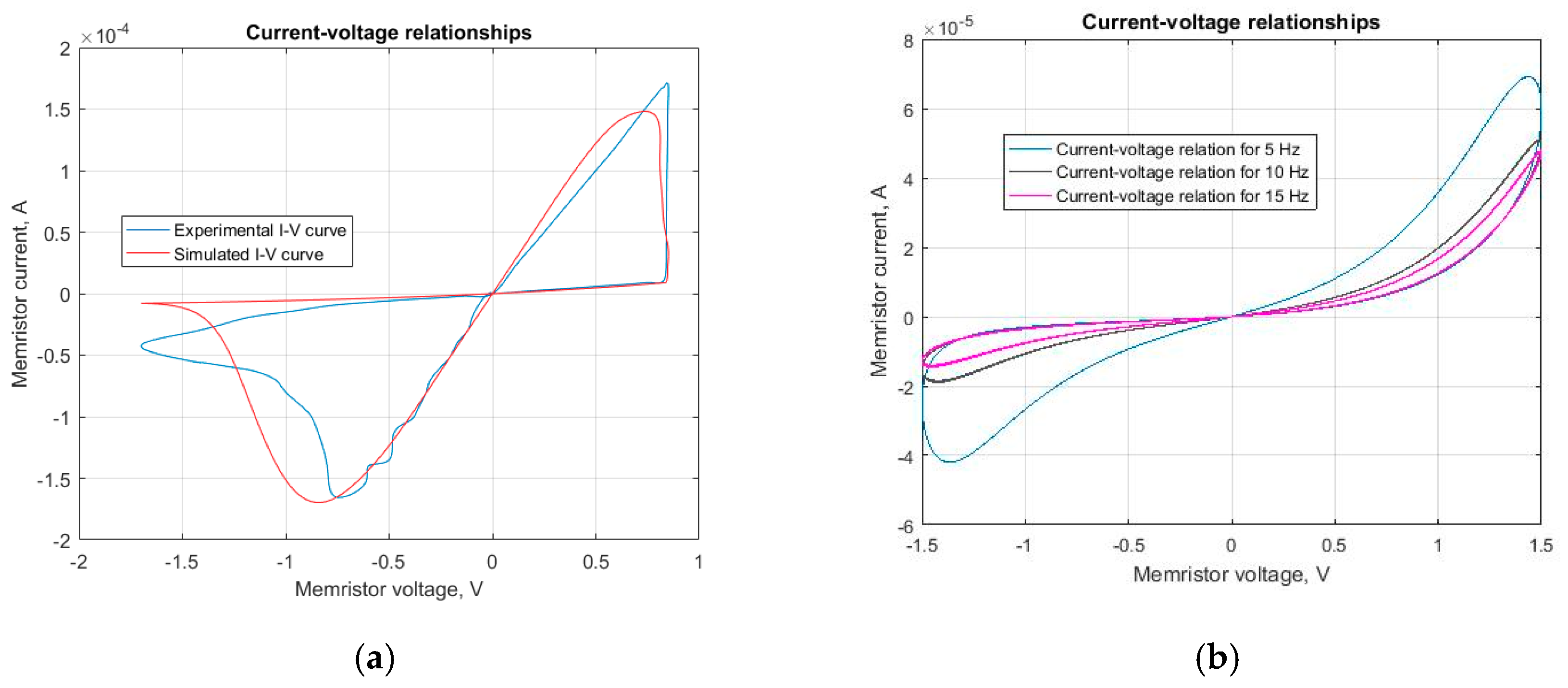
where the last equation in Equation (8) is the current–voltage relationship of the memristor element given in Equation (1). The applied modified mathematical Biolek’s memristor model is fully described by Equation (8) [7,8,14]. The corresponding current–voltage characteristic of the memristor element [7,8,14] is acquired after several simulations and adjusting the modified memristor model according to the [10]. This relationship is found using computer simulations in the MATLAB environment [18] and is plotted in Figure 1a to illustrate the closeness between the simulated and the experimental current–voltage characteristics.
3. Parameter Estimations of the Considered Memristor Model
The applied methodology for memristor model parameter estimations is founded on altering the memristor fitting parameters and searching for a global minimum of the root mean square error between the experimental and the obtained simulated current–voltage characteristics [15,16]. All the tuning coefficients of the model in Equation (8) were changed independently from one another. In the beginning of this procedure, very large intervals for varying the adjusting parameters were chosen (from 0 to 1000), and their minimal limits were used for initial values of the needed fitting parameters. One of the adjusted parameters was changed using constant step sizes between the values of the considered model parameter. The corresponding root mean square error between the experimentally recorded and the derived simulated current–voltage characteristics was calculated. The altering of the other adjusted memristor model parameters followed independently of one another [16].
During this procedure, a visual observation of the obtained current–voltage characteristic and its proximity to the experimental one was established. The basic criterion for stopping the described calculation procedure was the minimization of the root mean square error between the current–voltage relationships of the memristor element. Additional experiments were made around the derived optimal values of the fitting parameters using reduced steps for their changes [15]. The optimal values of the fitting model parameters were further used for testing the memristor model in memristor circuits and devices, and for analysis of the basic characteristics, namely current–voltage and state–flux relationships. In Mohammad et al. [9], several tentative values of the adjusting parameters α, β, γ, and χ are given. They were applied to start a multi-factor analysis [15,16] of the derived current–voltage characteristics of the hafnium dioxide memristor model. This analysis was made in the vicinity of the initial values of the adjusting parameters. In the beginning of the factor analysis, the change of the fitting model parameters was about 10% of their respective initial values, and when a proximity between the simulated and the experimental current–voltage curves was recognized, the change in these adjusting parameters was decreased to 2%. After a comparison of the derived i–v relationship of the memristor with the experimental current–voltage characteristics for the combinations of the adjusting parameters, the above presented values were derived for the best approximate matching between the simulated and the experimental current–voltage relationships [15].
The best possible memristor model parameters were also estimated using the least squares algorithm in the Simulink Design Optimization Toolbox and the Global Optimization Toolbox in the MATLAB environment [18]. The last toolbox was applied for finding the global minimum of the cost function, having in mind the assumption that it could contain several local minima [24]. A simulated annealing method was used for finding the global minimum of the cost function [25].
The least squares algorithm applied here was as follows. In the beginning of the simulation, the initial values of the adjusting model parameters were chosen. They were placed between their previously determined minimal and maximal limits. All the applied signals were formerly sampled in the time domain. The input signal of the algorithm was the memristor voltage u1. The experimental value of the output signal (the memristor current) was denoted by imes. The calculated output signal was the derived value of the memristor current icalc, in accordance with the hafnium dioxide memristor model. The cost function Scost was defined as a sum of the squares of the differences between the computed and the experimental output signal’s samples [15,16]:
where N is the number of signal samples. In the first iteration, the cost function was computed using the model parameters’ initial values. The criterion for stopping the described algorithm was the minimization the value of the cost function. Its minimum was reached when its partial derivatives with respect to all the memristor model parameters were zero [16]:
where ε is the vector of the adjusting parameters [14]:
For the next iteration of the considered algorithm, the model parameters’ values were changed by very low increments. The defined cost function was calculated again. Its derivatives according to the memristor model parameters were expressed. The parameters’ increments were chosen such that the cost function was decreasing. The optimal model parameters’ values were derived when the cost function was minimized [5,16].
The errors for the applied memristor model according to the used methodology were 4.2% for the considered modified model versus 4.6% for the original Lehtonen–Laiho model with the standard Biolek window [4,5]. The derived error according to the estimated parameters was 3.81% for the modified hafnium dioxide model. The simulation time of the considered model was 0.104 s, and for the existing model [11], it was 0.127 s. The obtained errors found using the applied methodology and using the least squares algorithm were almost equal. This confirmed the ability of the applied methodology to efficiently extract the memristor model parameters. An advantage of the considered modified model is the lower error with respect to the classical hafnium dioxide memristor model [5]. Another advantage of the modified model is its ability for realistic representation of the nonlinear ionic drift for high-level and high-frequency signals [5].
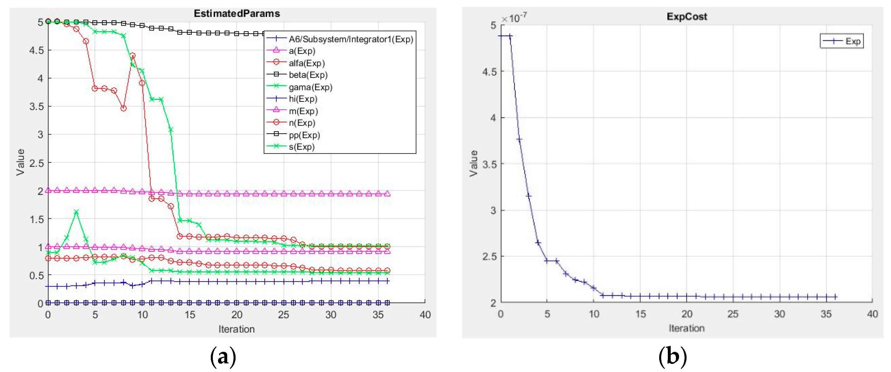
The change of the fitting parameters for the modified hafnium oxide memristor model during the estimation procedure realized in the MATLAB environment is presented in Figure 1a to visualize the estimating processes till the optimal values were found. The decreasing cost function during the parameter extraction process is presented in Figure 1b.
4. Analysis of the Considered Hafnium Oxide Memristor Model in the PSpice Environment
After finishing the tuning procedures and acquiring a good similarity between the experimental data [11] and the derived simulated current–voltage relationship (Figure 2a), an analysis of the considered memristor model was made in the OrCAD PSpice environment [5]. A PSpice substituting macro-model of the present mathematical memristor model was derived using Equation (8). The schematic of the memristor model was based on the mathematical operations in Equation (8) and it was created using the standard functional blocks in PSpice [5,19]. The PSpice library model of the hafnium dioxide memristor given in Appendix A was based on the considered substituting macro-model. Several i–v curves of the HfO2 memristor derived in the PSpice environment for different frequencies (5 Hz, 10 Hz, and 20 Hz) are presented in Figure 2b to illustrate the decrease of the area of the pinched hysteresis loop for higher-frequency signals. The observed result confirmed the main properties of the hafnium dioxide memristor element that were expressed using the applied mathematical model, namely passivity [26], memory effect [27], and high nonlinearity [28]. Although the memristor operated in a soft-switching mode, the state variable changed in broad range between 0.1 and 0.65.
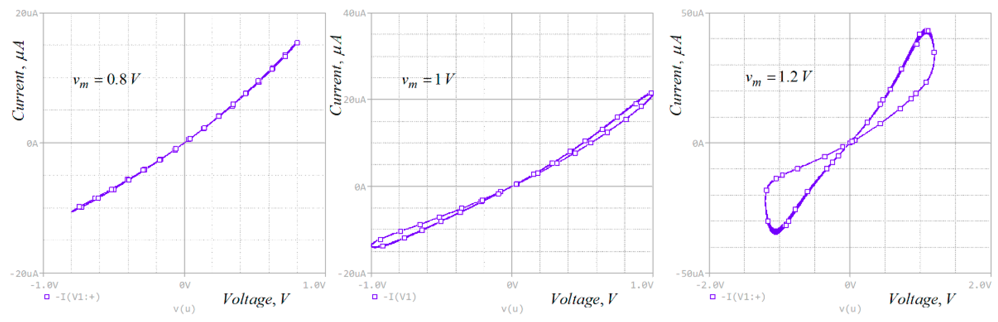
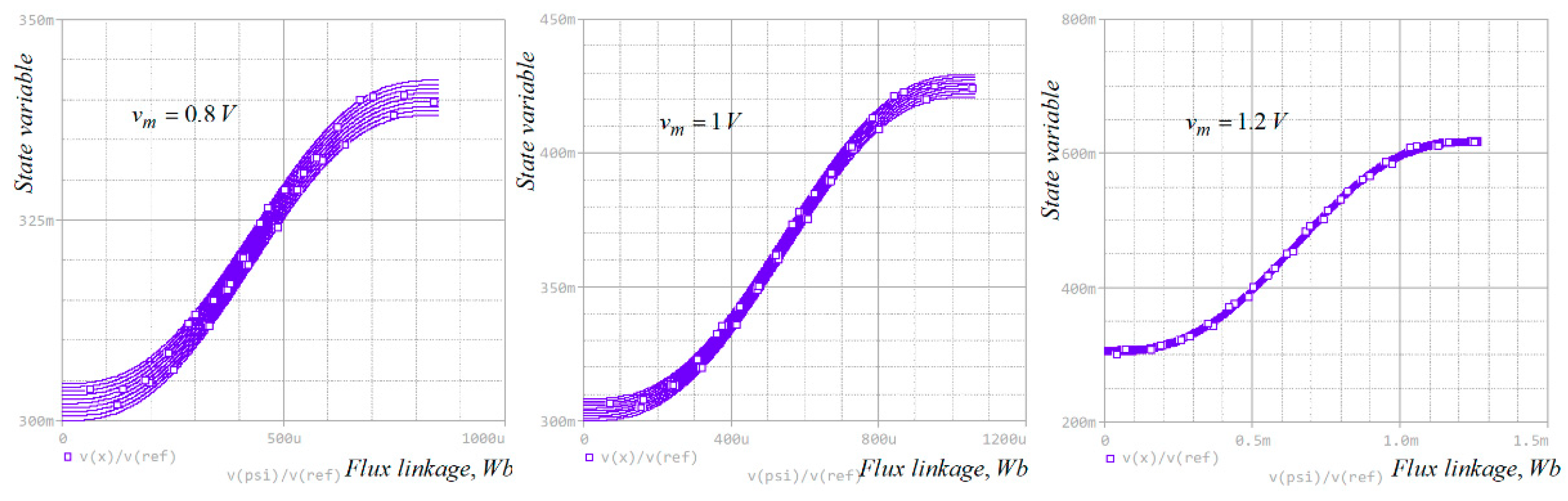
According to the previously described PSpice model of the hafnium dioxide memristor, several current–voltage relationships derived for different voltage amplitudes using a frequency of 3 kHz and sinusoidal mode are presented in Figure 3. They provide confirmation of the performance and the correct operation of the considered PSpice memristor model, where increasing the signal’s amplitude caused the area of the current–voltage pinched hysteresis loop to increase too. The considered hafnium dioxide memristor model was simulated using sine-wave voltage signals with several different amplitudes and frequencies, and convergence problems were not observed. The derived i–v curves were symmetrical for soft-switching mode and non-symmetrical for states near the hard-switching mode due to the internally applied non-symmetrical current–voltage relationship and the presence of the corresponding two terms in Equation (1), namely the hyperbolic sine and exponential terms that describe tunneling and semiconducting effects, respectively. The corresponding state–flux relations are presented in Figure 4 to demonstrate their almost single- and multi-valuedness for the soft-switching and hard-switching modes, respectively.
5. Application and Testing of the Proposed Hafnium Oxide Memristor Model
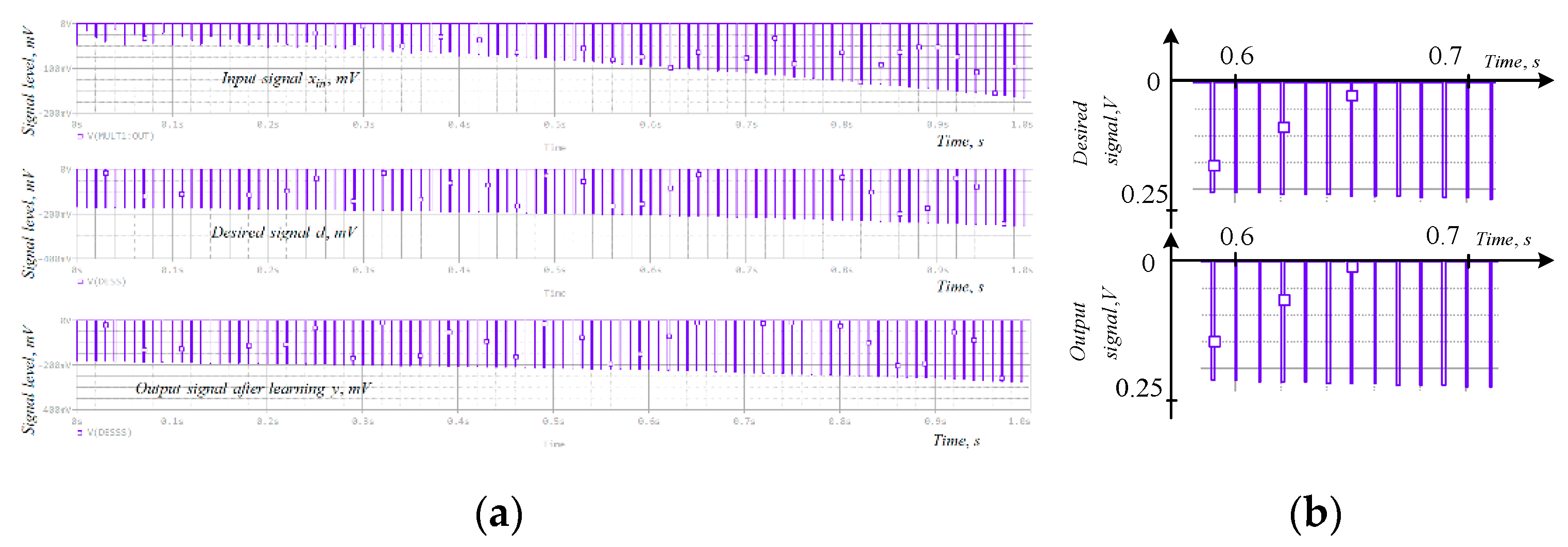
The considered hafnium oxide memristor model was used in a simple multilayer neural network for function fitting [20]. It used memristor-resistor synaptic bonds [21,23,26]. The schematic of the neural network is presented in Figure 5. The considered multilayer neural network was used for fitting the input signal x according to the desired signal d. The input signal applied to the network and expressed in the time domain was x = 0.055[1 –exp(t + 0.4)] + 0.02exp(−4t)sin(2π × 40t) V. This signal was sampled using a short rectangular pulse sequence with a frequency of 50 Hz [14]. The respective desired signal was d = 0.025[1 – exp(1.5t)] − 0.17 V and it was sampled with the same sampling pulses. The pauses between the corresponding values of the used signals were applied for tuning the synaptic weights [20]. These signals were applied for a time interval with a duration of 1 s such that it could be concluded that an epoch had a length of 1 s. The considered neural network contained five neurons in the hidden layer and one neuron with a linear activation function in the output layer [5]. The principle of operation of the considered memristor-based neural network was based on a supervised learning, backpropagation error correction algorithm, and on tuning the synaptic weights [5,20]. The neurons in the hidden network’s layer used a sigmoid activation function [5]. The synapses in the neural network were based on hafnium dioxide memristors and they were made according to the bridge schematic topology expressed in Mladenov [21]. A schematic of the applied memristor-based synapses is presented in Figure 6a to display their structure and principle of operation. This type of synapse was made using a bridge schematic topology and it was suitable for storing synaptic weights, both with positive, zero, and negative values. The synapses in the hidden layer are denoted by V1, V2, V3, V4, and V5. The synaptic bonds in the output layer are denoted by W1, W2, W3, W4, and W5, respectively.
The input and output signals of the considered memristor-based synapses were denoted using vin and vout, respectively. The transfer function (synaptic weight) of the described synapse (Figure 6a) was [14,21]:
Based on the value of the resistance of the memristor M, the synaptic weight w could have a positive, zero, or negative value [21]. The resistances of the used resistors were R2 = 550 Ω, R3 = 120 Ω, andR4 = 120 Ω. The weight of the memristor synapse was altered by applying input voltage impulses. The considered neural network was first simulated and the synaptic weights were tuned in MATLAB [18]. After the teaching of the neural network, the resistances of the memristors in the synapses obtained stable and constant values [5]. After the learning process, the neural network was able to fit the input data. The input, desired, and output signals are presented in Figure 6b for the comparison of the output and the desired signals of the multilayer neural network after the learning procedure. These signals were almost equal one to another when the elapsed time was longer than 0.5 s; the difference between them was 0.002 V or 1.82% of the value of the desired signal. In the initial moment of the investigation of the network, all the synaptic weights were zeros. After finalizing the learning procedure, they obtained the correct and constant values. The biases of the input layer b1n; the weights of the bias of the hidden layer of the neural network b2; the synaptic weights for the input layer v1n; the synaptic weights for the hidden layer w; and the respective resistances Mb1, Mb2, and Mw of the memristors are presented in Table 1. The number n presents the respective synapse in the network.
The learned neural network with tuned memristor synapses was simulated in the PSpice environment. The variation in time of the signals derived in PSpice are presented in Figure 7a to illustrate their similarity to those obtained in the MATLAB environment (Figure 6). A zoomed diagram is presented in Figure 7b for a detailed comparison of the signals. If the time was t = 0.5 s, then the difference between the output and the desired signals was about 1.9 mV, or about 1.8% of the value of the desired signal. The average value of the relative error was near 3%.
A good closeness between the obtained signals was obtained (Figure 6 and Figure 7). This confirmed the capability of the considered memristor neural network for function fitting and the proper operation of the used hafnium oxide memristor model for the memristors in the synapses. The considered model is applicable not only for hafnium-dioxide memristors but also for titanium dioxide memristors because it was based on the Lehtonen–Laiho model [8]. The main advantages of the considered model with respect to the existing hafnium dioxide models are its capability for operation at signals with high amplitudes and frequencies, the possibility for tuning, the higher accuracy, and realistic representation of the ionic motion for high signal levels. An advantage of the presented memristor model according to several other modified author’s models [23] is the use of a continuous and differentiable function instead of the step function, and therefore the reduced occurrence of convergence problems. According to the main existing models [28], the considered model more realistically represents the ionic dopant drift and the switching effects for high-amplitude and high-frequency signals.
6. Conclusions
The highly nonlinear drift memristor model with a modified window function used in this research, which was proposed by the author in another paper, was successfully adjusted to experimentally record the current–voltage characteristic of a HfO2-based memristor element. For the fitting procedure, a minimization of the root mean square error between the current–voltage characteristics was applied. The comparison between the experimental and the simulated current–voltage relations produced a reasonable closeness between the corresponding relationships. After a tuning procedure, the considered hafnium dioxide memristor model was simulated in the OrCAD PSpice environment for voltage signals with different magnitudes and frequencies. The considered hafnium dioxide memristor model was successfully applied and tested in a simple multilayer neural network for function fitting with memristor–resistor bridge synapses. The correct operation of the memristor-based neural network was confirmed for both the learning and the fitting processes analyzed in the time domain. The main advantages of the proposed modified HfO2memristor model are its relative simplicity for realization in the PSpice environment, the lack of convergence problems due to the use of a differentiable tangent hyperbolic function instead of the non-differentiable step function, and the realistic representation of the nonlinearity of the ionic dopant drift in the memristor element due to the higher nonlinearity of the modified window function used and the corresponding current–voltage relation.
Funding
This research received no external funding.
Conflicts of Interest
The author declares no conflict of interest.
Appendix A
*PSpice code of the considered memristor model
.subckthfo a c
V_CONST10HI 0 DC 30e-6
V_CONST1A 0 DC 230
E_ABM4FW1 0 VALUE {
+(((1-pwrs((V(x)-V(st)),V(dvepe))))+(V(mm)*(sin(3.14*V(x)))*(sin(3.14*V(x)))))/(V(mm)+1)
+}
G_ABMII1A C VALUE { (V(IM))}
V_CONST4C 0 DC 3
E_DIFF2N12206 0 VALUE {V(N12130,N12164)}
R_R1A N110561 TC=0,0
V_CONST8BETA 0 DC 90e-6
E_ABM6GPLUS 0 VALUE { 1/((1+exp(-50*(V(TT)))))}
E_MULT2N11926 0 VALUE {V(N11854)*V(N11904)}
V_CONST7FW2 0 DC 0
E_EXP1N12130 0 VALUE {EXP(V(N12092))}
V_CONST6ALFA 0 DC 1.9
E_ABM9ST 0 VALUE { 1/((1+exp(-50*(V(U)))))}
V_CONST11N12164 0 DC 1.000
E_ABM7GMINUS 0 VALUE { 1/((1+exp(50*(V(TT)))))}
X_INTEG1N11330 X SCHEMATIC1_INTEG1
E_ABM10N11854 0 VALUE { (exp((V(N11818)))-exp(-(V(N11818))))/(2)}
E_MULT4N12092 0 VALUE {V(GAMA)*V(U)}
V_CONST9GAMA 0 DC 0.5
R_R3C 01g TC=0,0
X_INTEG2U PSI SCHEMATIC1_INTEG2
E_PWRS1N11904 0 VALUE {PWRS(V(X),5)}
E_ABM8N11330 0 VALUE {
+V(a)*pwrs(V(u),V(m))*(V(FW1))*V(gplus)+V(gminus)*V(fw2)}
E_MULT1N11818 0 VALUE {V(ALFA)*V(U)}
V_CONST2M 0 DC 5
V_CONST5THR 0 DC 0.2
E_ABM5TT 0 VALUE { (abs(V(U))-V(thr))}
E_MULT5N12250 0 VALUE {V(HI)*V(N12206)}
E_DIFF1U 0 VALUE {V(N11056,C)}
V_CONST3B 0 DC 20
R_R2N11056 C1g TC=0,0
E_SUM1IM 0 VALUE {V(N11990)+V(N12250)}
E_MULT3N11990 0 VALUE {V(BETA)*V(N11926)}
V_CONST12DVEPE 0 DC 10
V_CONST13MM 0 DC 0.7
.ends
.subckt SCHEMATIC1_INTEG1 in out
G_INTEG10 $$U_INTEG1 VALUE {V(in)}
C_INTEG1$$U_INTEG1 0 {1/1.0}
R_INTEG1$$U_INTEG1 0 1G
E_INTEG1out 0 VALUE {V($$U_INTEG1)}
.ICV($$U_INTEG1) = 0.3
.ends SCHEMATIC1_INTEG1
.subckt SCHEMATIC1_INTEG2 in out
G_INTEG20 $$U_INTEG2 VALUE {V(in)}
C_INTEG2$$U_INTEG2 0 {1/1.0}
R_INTEG2$$U_INTEG2 0 1G
E_INTEG2out 0 VALUE {V($$U_INTEG2)}
.ICV($$U_INTEG2) = 0V
.ends SCHEMATIC1_INTEG2
References
- Chua, L. Memristor—The Missing Circuit Element. IEEE Trans. Circuit Theory 1971, 18, 507–519. [Google Scholar] [CrossRef]
- Strukov, D.; Snider, G.; Stewart, D.; Williams, R. The Missing Memristor Found. Nat. Lett. 2008, 453, 80–83. [Google Scholar] [CrossRef] [PubMed]
- Joglekar, Y.; Wolf, S. The Elusive Memristor: Properties of Basic Electrical Circuits. Eur. J. Phys. 2009, 30, 661–675. [Google Scholar] [CrossRef] [Green Version]
- Biolek, Z.; Biolek, D.; Biolkova, V. SPICE Model of Memristor with Nonlinear Dopant Drift. Radioengineering 2009, 18, 210–214. [Google Scholar]
- Mladenov, V. A New Simplified Model for HfO2-Based Memristor. In Proceedings of the 2019 8th International Conference on Modern Circuits and Systems Technologies (MOCAST), Thessaloniki, Greece, 13–15 May 2019. [Google Scholar]
- Strukov, D.; Williams, R.S. Exponential ionic drift: Fast switching and low volatility of thin-film memristors. Appl. Phys. A 2009, 4, 515–519. [Google Scholar] [CrossRef]
- Yang, J.; Pickett, M.; Li, X.; Ohlberg, D.; Stewart, D.; Williams, R. Memristive switching mechanism for metal/oxide/metal nanodevices. Nat. Nanotechnol. 2008, 3, 429–433. [Google Scholar] [CrossRef] [PubMed]
- Lehtonen, E.; Laiho, M. CNN using memristors for neighborhood connections. In Proceedings of the 2010 12th International Workshop on Cellular Nanoscale Networks and their Applications, Berkeley, CA, USA, 3–5 February 2010. [Google Scholar]
- Mohammad, B.; Jaoude, M.; Kumar, V.; Homouz, D.; Nahla, H.; Al-Qutayri, M.; Christoforou, N. State of the art of metal oxide memristor devices. Nanotechnol. Rev. 2016, 5, 311–329. [Google Scholar] [CrossRef]
- Lupo, N.; Bonizzoni, E.; Pérez, E.; Wenger, C.; Maloberti, F. A Voltage–Time Model for Memristive Devices. IEEE Trans. Very Large Scale Integr. Syst. 2018, 26, 1452–1460. [Google Scholar] [CrossRef]
- Amer, С.; Sayyaparaju, S.; Rose, G.; Beckmann, K.; Cady, N. A practical hafnium-oxide memristor model suitable for circuit design and simulation. In Proceedings of the 2017 IEEE International Symposium on Circuits and Systems (ISCAS), Baltimore, MD, USA, 28–31 May 2017; pp. 1–5. [Google Scholar]
- Matveyev, Y.; Kirtaev, R.; Fetisova, A.; Zakharchenko, S.; Negrov, D.; Zenkevich, A. Crossbar Nanoscale HfO2-Based Electronic Synapses. Nanoscale Res. Lett. 2016, 11, 1–6. [Google Scholar] [CrossRef] [PubMed] [Green Version]
- Kumar, S.; Wang, Z.; Huang, X.; Kumari, N.; Davila, N.; Strachan, J.; Vine, D.; Kilcoyne, A.; Nishi, Y.; Williams, R. Oxygen migration during resistance switching and failure of hafnium oxide memristors. Appl. Phys. Lett. 2017, 110, 103503. [Google Scholar] [CrossRef] [Green Version]
- Mladenov, V.; Kirilov, S. A Nonlinear Drift Memristor Model with a Modified Biolek Window Function and Activation Threshold. Electronics 2017, 6, 77. [Google Scholar] [CrossRef] [Green Version]
- Zhou, J.; Shi, J. A comprehensive multi-factor analysis on RFID localization capability. Adv. Eng. Inform. 2011, 25, 32–40. [Google Scholar] [CrossRef]
- Chen, S.; Billings, A.; Luo, W. Orthogonal least squares methods and their application to non-linear system identification. Int. J. Control 1989, 50, 1873–1896. [Google Scholar] [CrossRef]
- Ntinas, V.; Ascoli, A.; Tetzlaff, R.; Sirakoulis, G. Transformation techniques applied to a TaO memristor model to enable stable device simulations. In Proceedings of the 2017 European Conference on Circuit Theory and Design, Catania, Italy, 4–6 September 2017. [Google Scholar]
- Palm, W. Introduction to MATLAB for Engineers; McGraw-Hill: New York, NY, USA, 2011; ISBN 978-1-259-01205-1. [Google Scholar]
- Rashid, M. Introduction to PSpice Using OrCAD for Circuits and Electronics, 3rd ed.; Prentice Hall: Upper Saddle River, NJ, USA, 2004; ISBN 0-13-101988-0. [Google Scholar]
- Fausett, L. Fundamentals of Neural Networks; Prentice Hall: Upper Saddle River, NJ, USA, 1994; ISBN 0130422509. [Google Scholar]
- Mladenov, V. Synthesis and Analysis of a Memristor-Based Artificial Neuron. In Proceedings of the 16th International Workshop on Cellular Nanoscale Networks and their Applications, Budapest, Hungary, 28–30 August 2018. [Google Scholar]
- Mladenov, V.; Kirilov, S. Learning of an Artificial Neuron with Resistor-Memristor Synapses. In Proceedings of the Advances in Neural Networks and Applications, St. Konstantin, Bulgaria, 15–17 September 2018. [Google Scholar]
- Mladenov, V. Advanced Memristor Modeling—Memristor Circuits and Networks; MDPI: Basel, Switzerland, 2019; ISBN 978-3-03897-104-7. [Google Scholar]
- Liberti, L. Introduction to Global Optimization; LIX, Ecole Polytechnique: Palaiseau, France, 2008. [Google Scholar]
- Haddock, J.; Mittenthal, J. Simulation optimization using simulated annealing. Comput. Ind. Eng. 1992, 22, 387–395. [Google Scholar] [CrossRef]
- Chua, L. Resistance switching memories are memristors. Appl. Phys. A Mater. Sci. Process. 2011, 5, 765–783. [Google Scholar] [CrossRef] [Green Version]
- Walsh, A.; Carley, R.; Feely, O.; Ascoli, A. Memristor circuit investigation through a new tutorial toolbox. In Proceedings of the 2013 European Conference on Circuit Theory and Design, Dresden, Germany, 8–12 September 2013. [Google Scholar]
- Ascoli, A.; Tetzlaff, R.; Biolek, Z.; Kolka, Z.; Biolkovà, V.; Biolek, D. The Art of Finding Accurate Memristor Model Solutions. IEEE J. Emerg. Sel. Top. Circuits Syst. 2015, 5, 133–142. [Google Scholar] [CrossRef]
Figure 1.
(a) Model’s parameters change during the estimation process. (b) Minimization of the previously defined cost function.
Figure 1.
(a) Model’s parameters change during the estimation process. (b) Minimization of the previously defined cost function.

Figure 2.
(a) Current–voltage characteristics (experimental and simulated), derived after fitting the proposed HfO2 nonlinear memristor model; a reasonable matching between these characteristics was established. (b) Current–voltage relationships obtained for different frequencies: 5 Hz, 10 Hz, and 20 Hz; for lower frequencies, the current–voltage curve was asymmetric and the area of the pinched hysteresis loop decreased with increasing signal frequencies.

Figure 3.
Current–voltage relationships of the considered memristor model, derived in the PSpice environment for sinusoidal mode and several different amplitudes of the voltage signal. These relationships have non-symmetrical shapes due to the internally applied non-symmetrical relationship in the model.

Figure 4.
The corresponding state–flux relationships of the considered hafnium dioxide memristor model for sinusoidal mode and different voltage amplitudes.
Figure 4.
The corresponding state–flux relationships of the considered hafnium dioxide memristor model for sinusoidal mode and different voltage amplitudes.

Figure 5.
A memristor-based multilayer neural network for function fitting.

Figure 6.
(a) The applied synaptic circuit based on resistors and a memristor; the bridge structure of this circuit ensured negative, zero, and positive synaptic weights could be obtained. (b) Signal convergence over time of the input signal, desired signal, and output signal of the neural network, derived after the learning procedure; the desired and the output signal of the considered device, derived after learning using the neural network, almost matched each other when the elapsed time was longer than 0.5 s.

Figure 7.
(a)Variation over time of the input, output, and the desired signals of the neural network derived in PSpice after finishing the learning procedure. (b) A detailed zoomed region of the desired and the output signals.
Figure 7.
(a)Variation over time of the input, output, and the desired signals of the neural network derived in PSpice after finishing the learning procedure. (b) A detailed zoomed region of the desired and the output signals.


Table 1.
Values of the synaptic weights and the corresponding memristances.
| n | 1 | 2 | 3 | 4 | 5 |
|---|---|---|---|---|---|
| b1n | −0.45 | −0.45 | 0.01 | 0.05 | 0.31 |
| b1 | −0.0052 | - | - | - | - |
| v1n | 0.5997 | 0.9652 | −0.1571 | 0,1110 | 0.3220 |
| w1n | 0.0744 | 0.0720 | −0.2898 | 0.5309 | 0.1276 |
| Mb1n | 10450 | 10450 | 528.4 | 450 | 129.01 |
| Mb2 | 561.6 | - | - | - | - |
| Mv1n | 149.8 | 174.62 | 1053.96 | 350.16 | 119.09 |
| Mw1n | 407.52 | 411.53 | 2066.55 | 160.48 | 326.35 |
© 2020 by the author. Licensee MDPI, Basel, Switzerland. This article is an open access article distributed under the terms and conditions of the Creative Commons Attribution (CC BY) license (http://creativecommons.org/licenses/by/4.0/).
Share and Cite
MDPI and ACS Style
Mladenov, V.
A New Simplified Model and Parameter Estimations for a HfO2-Based Memristor
AMA Style
Mladenov V.
A New Simplified Model and Parameter Estimations for a HfO2-Based Memristor
Mladenov, Valeri.
2020. "A New Simplified Model and Parameter Estimations for a HfO2-Based Memristor
Note that from the first issue of 2016, this journal uses article numbers instead of page numbers. See further details here.