
Analysis, Simulation, and Development of a Low-Cost Fully Active-Electrode Bioimpedance Measurement Module

 ,
, 
Abstract
:1. Introduction
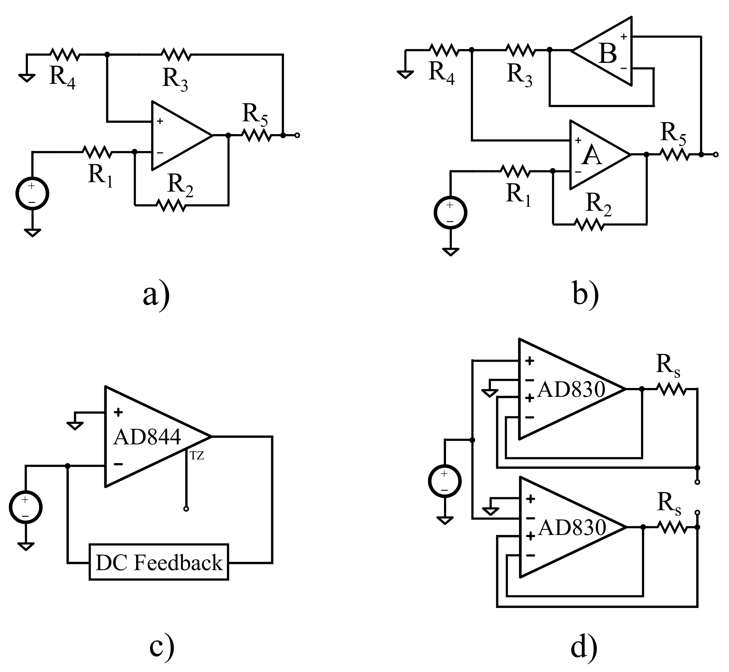
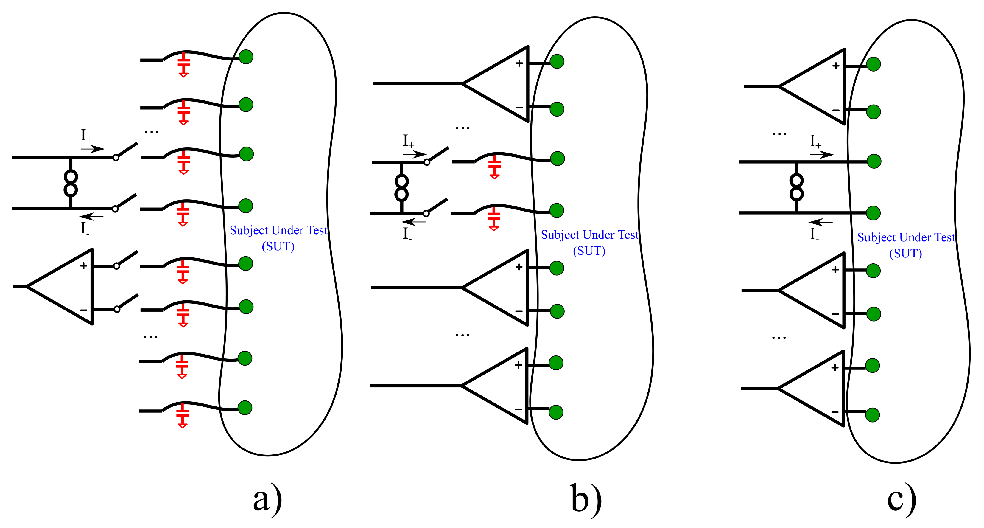
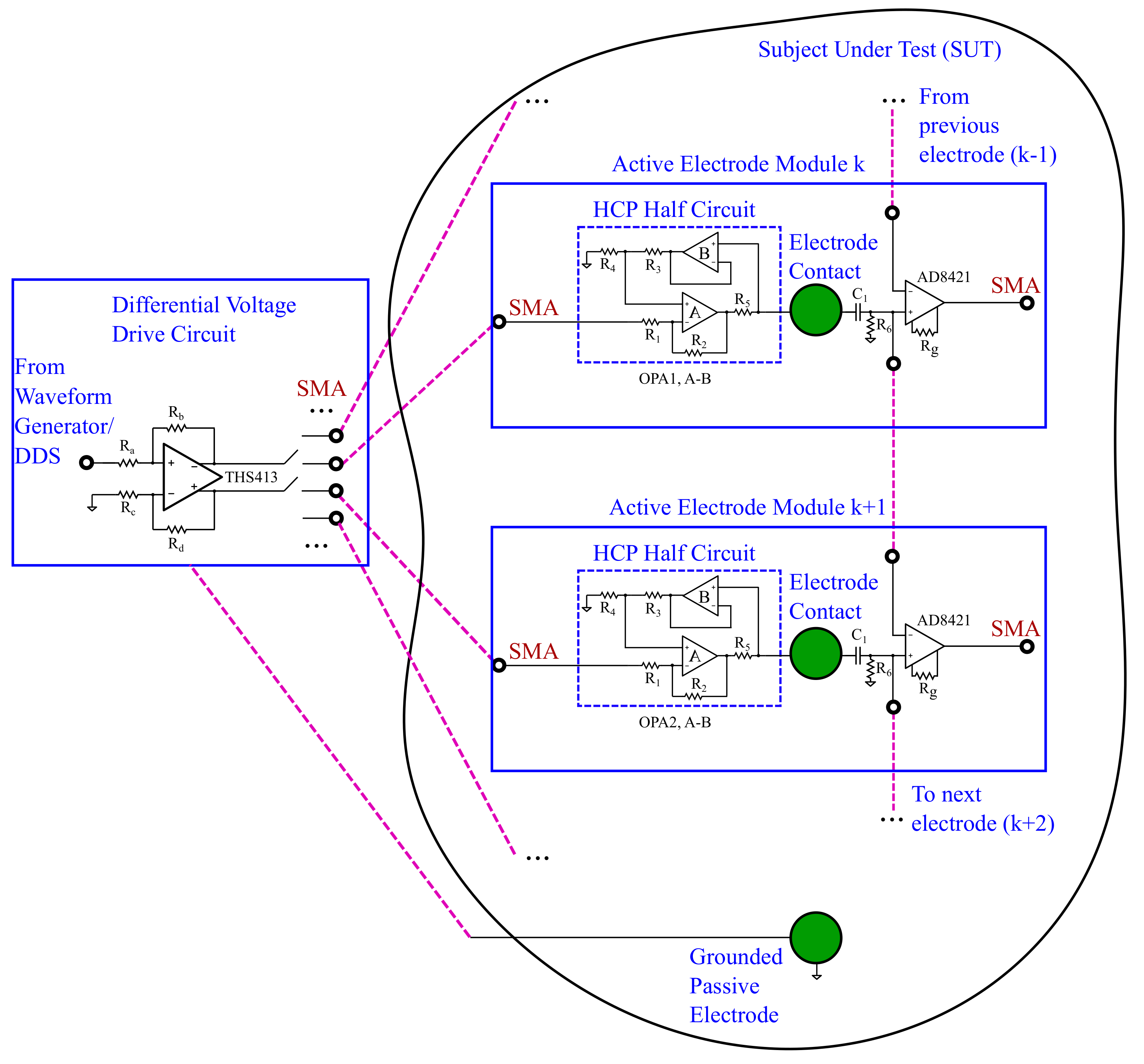
2. The Proposed Module
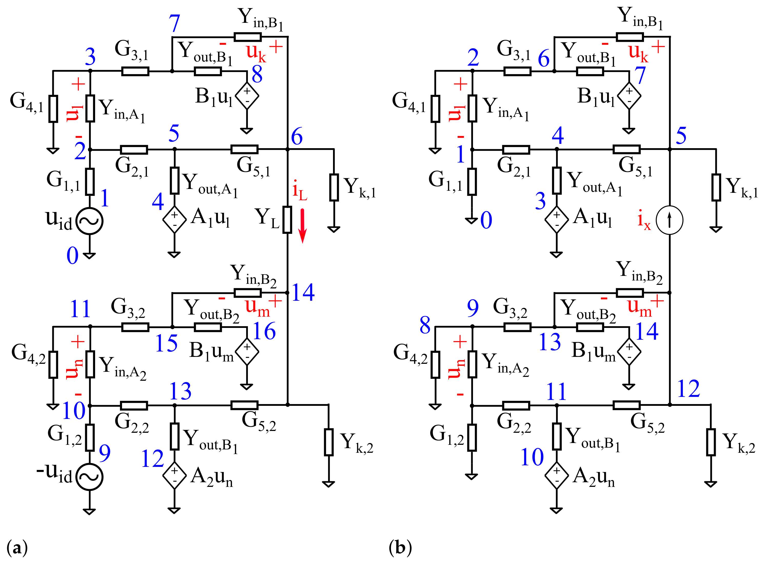
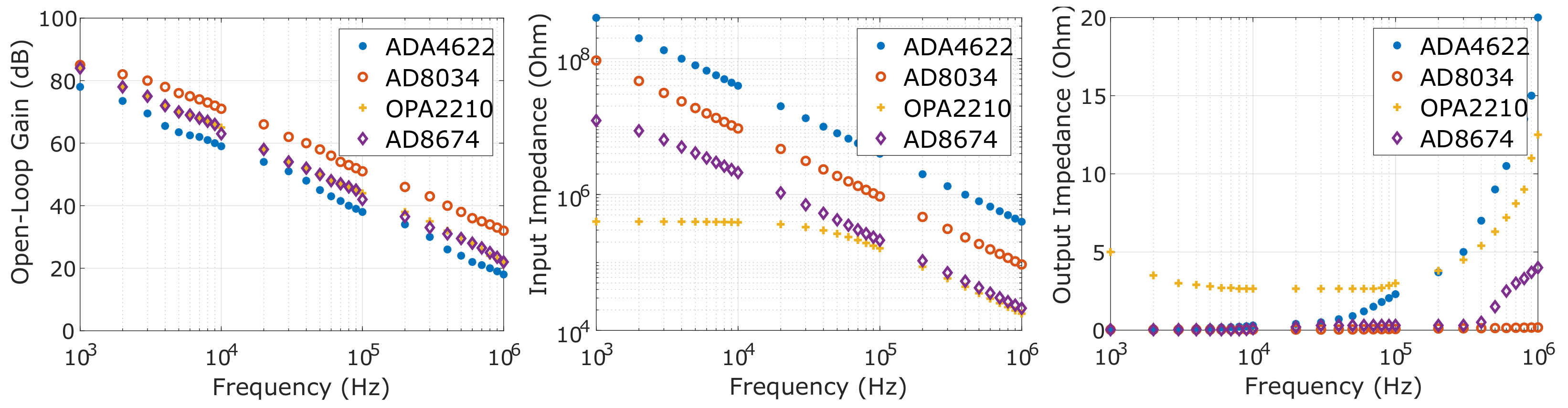
3. Circuit Analysis
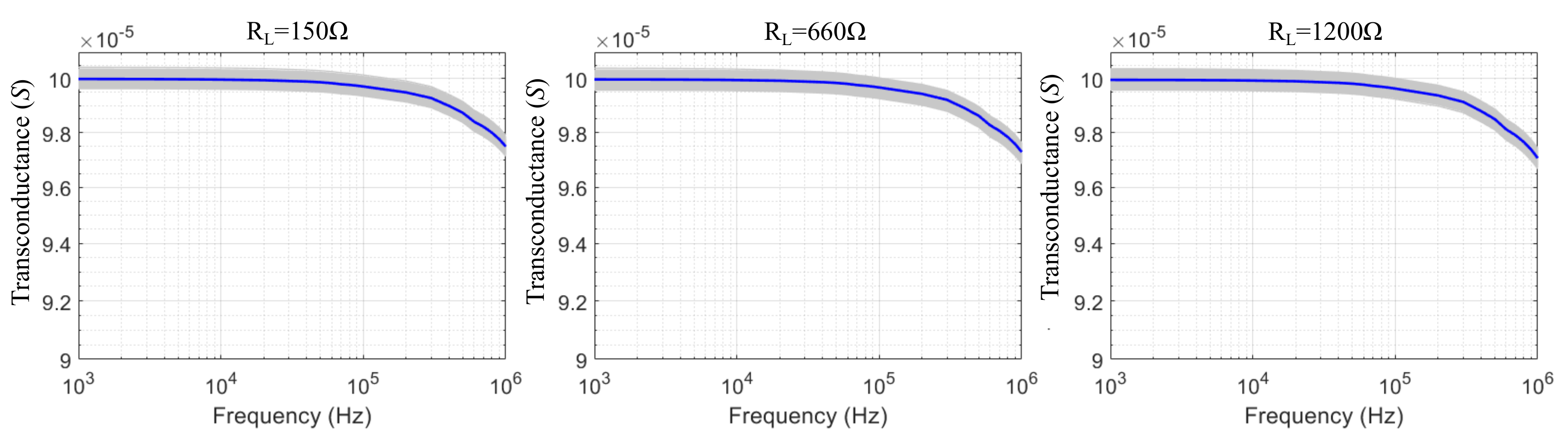
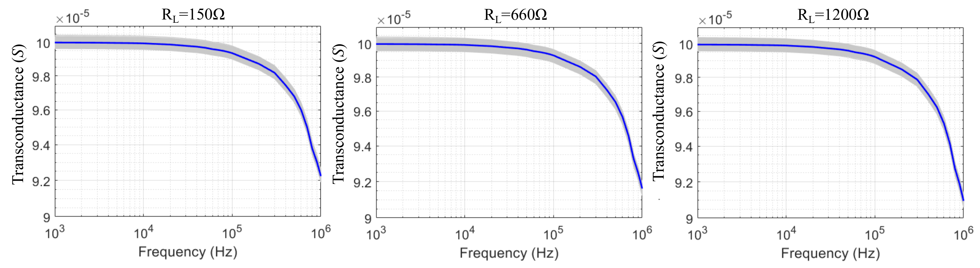
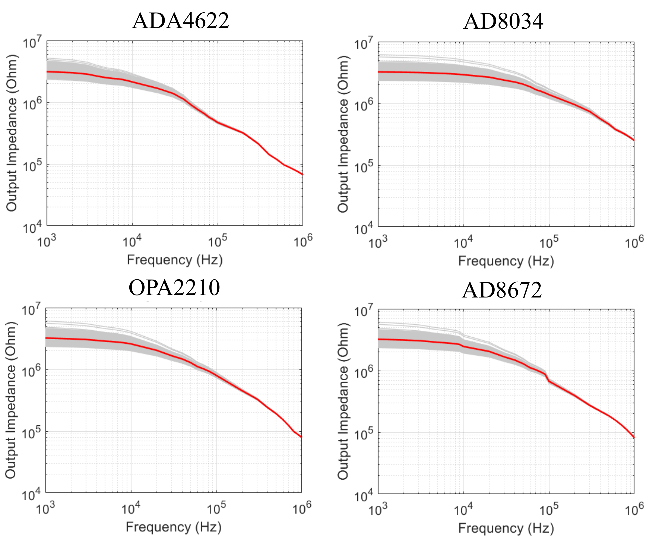
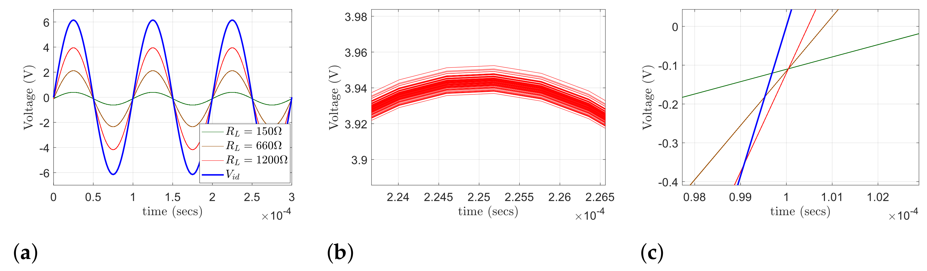
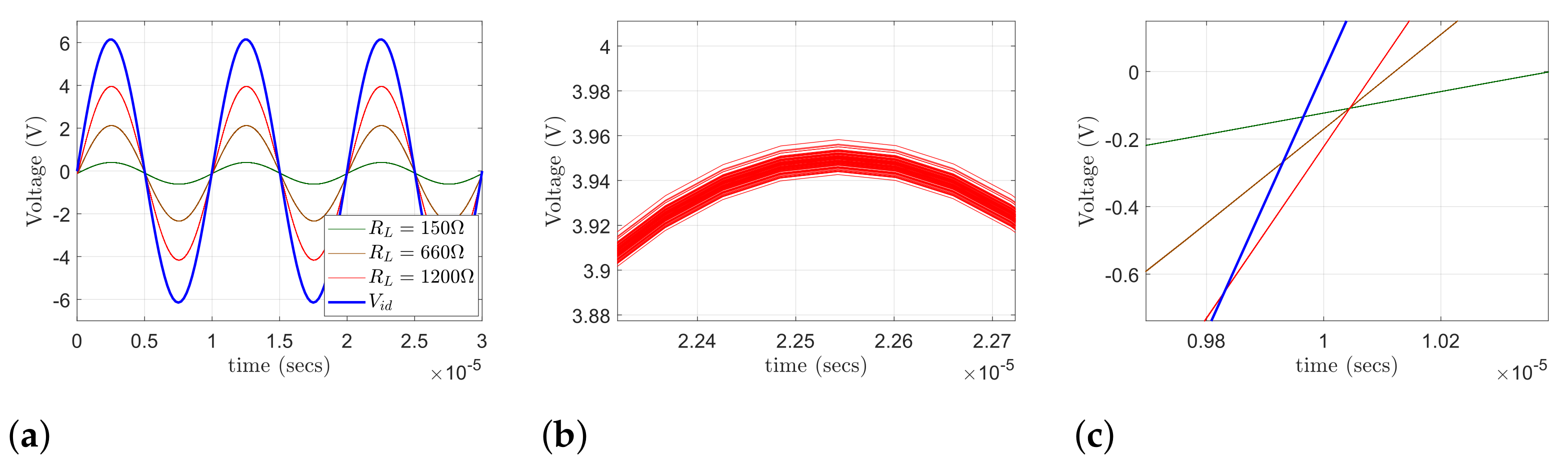
4. SPICE Simulations
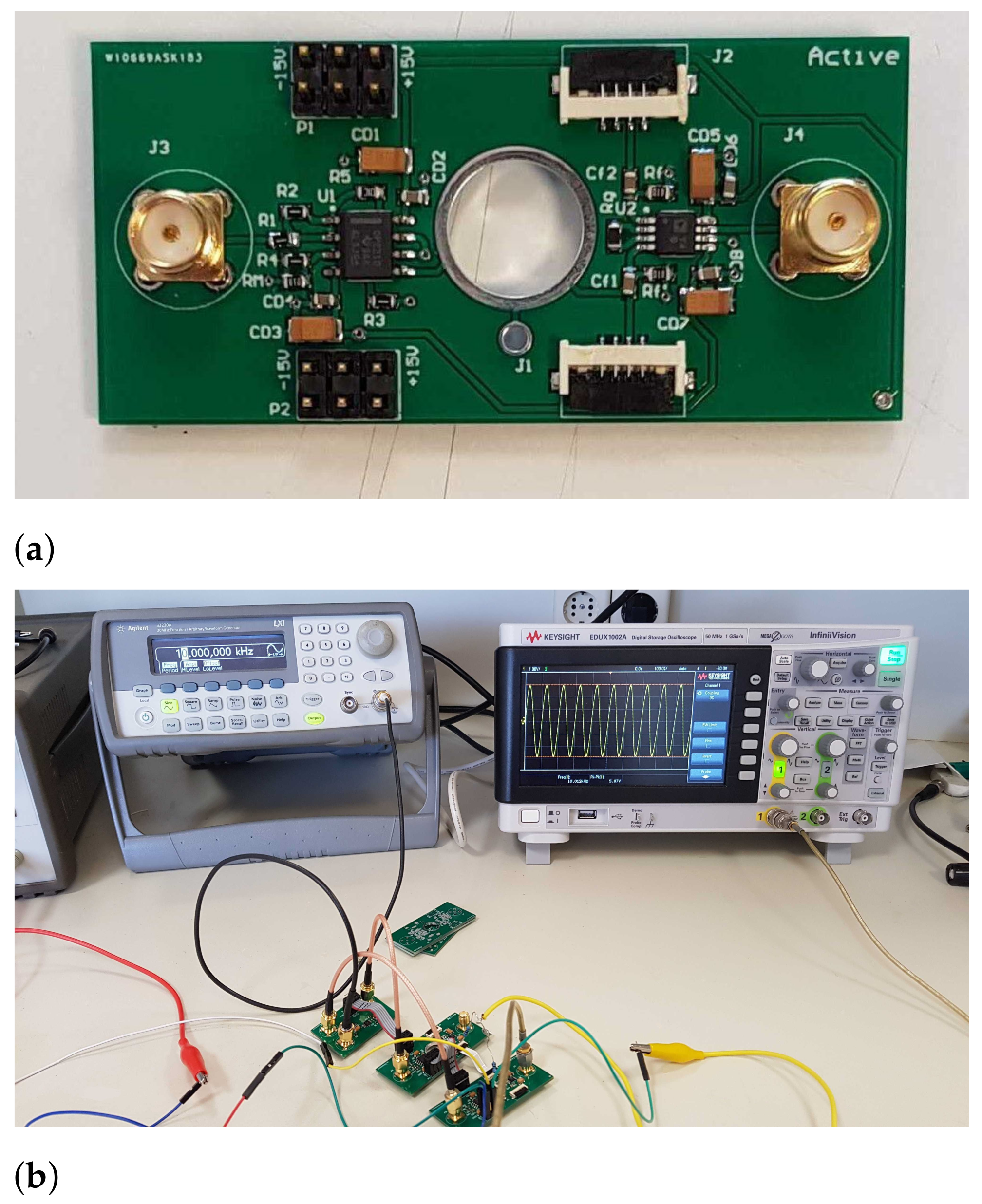
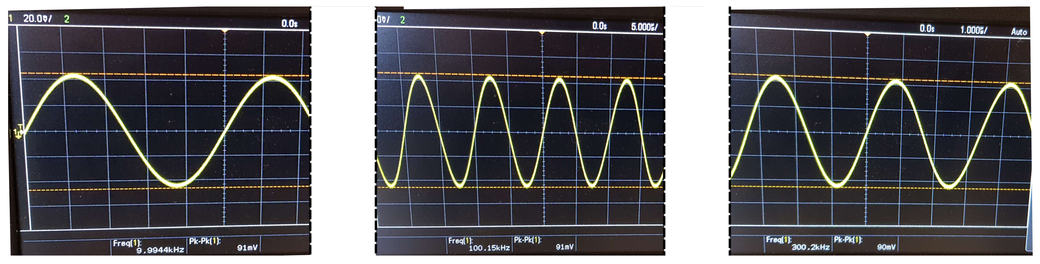
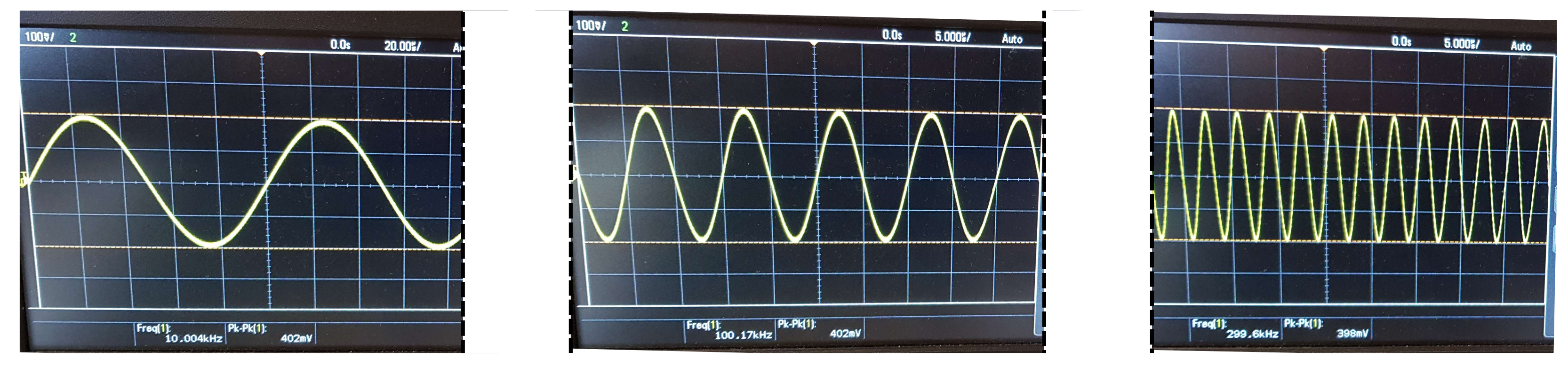
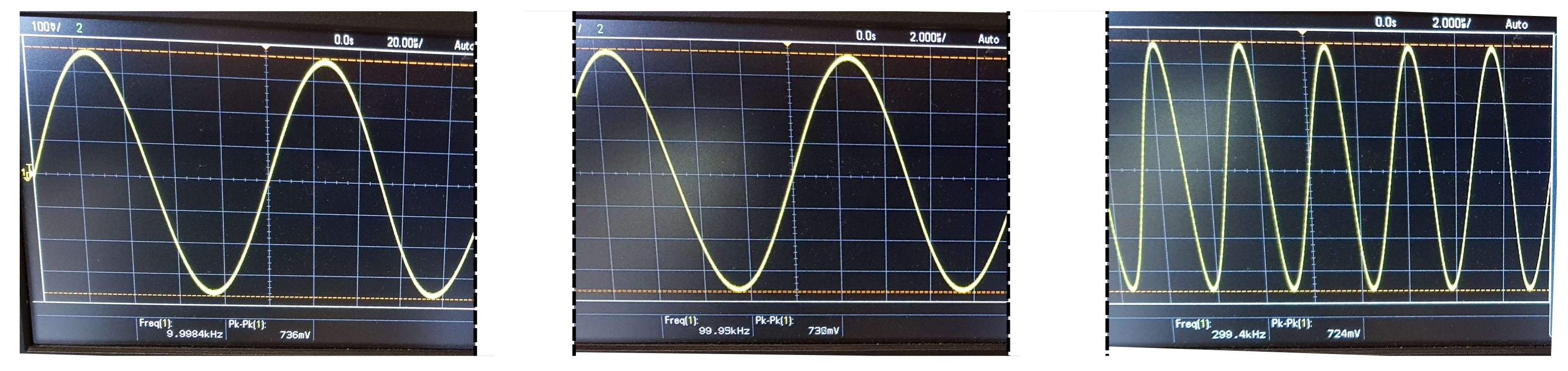
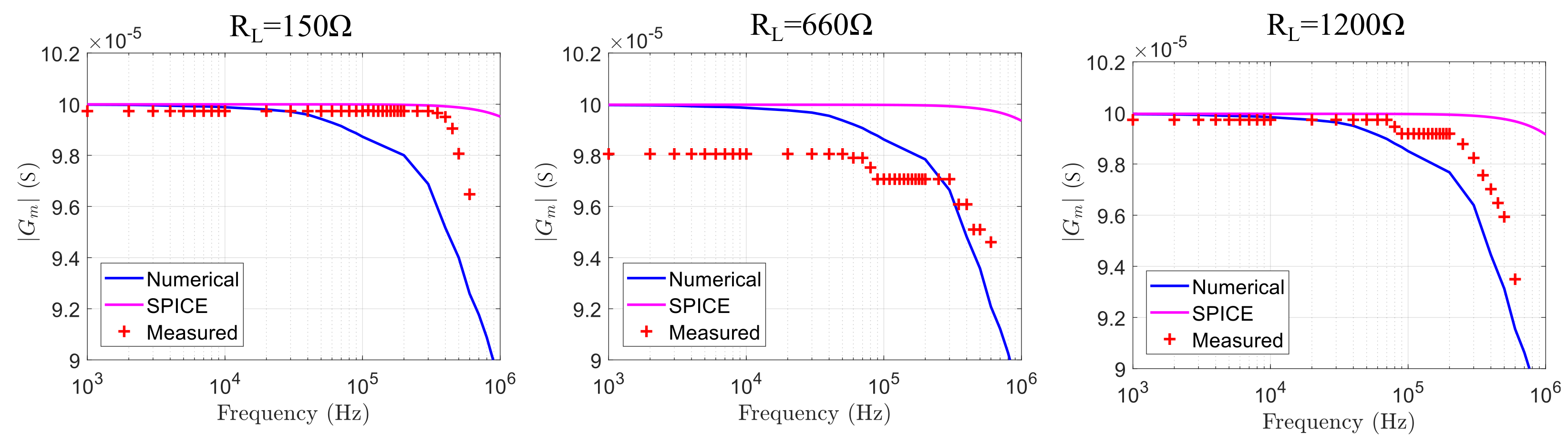
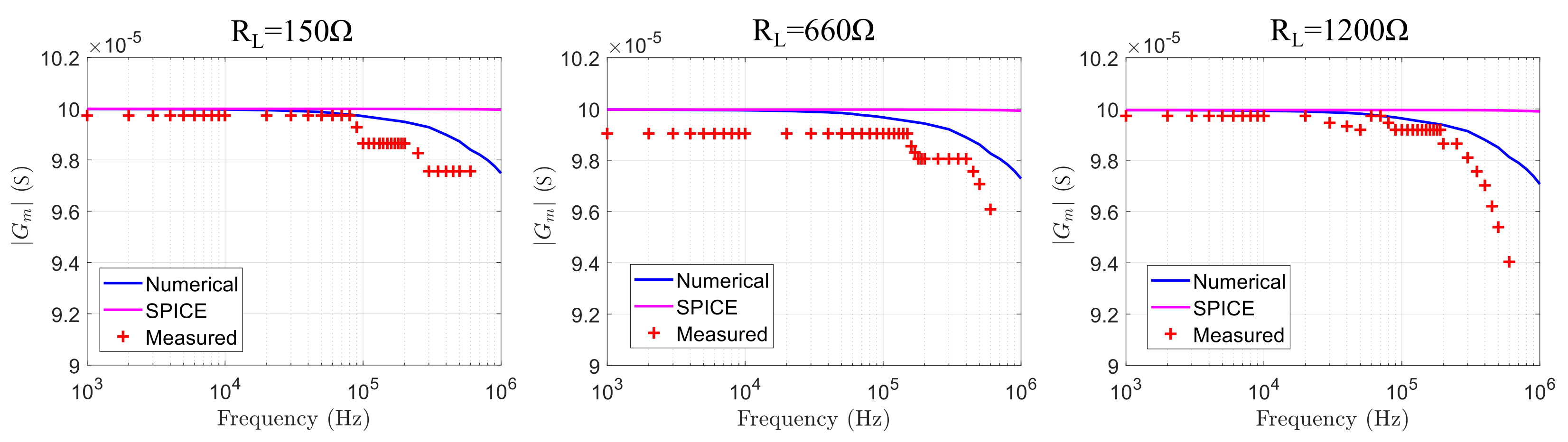
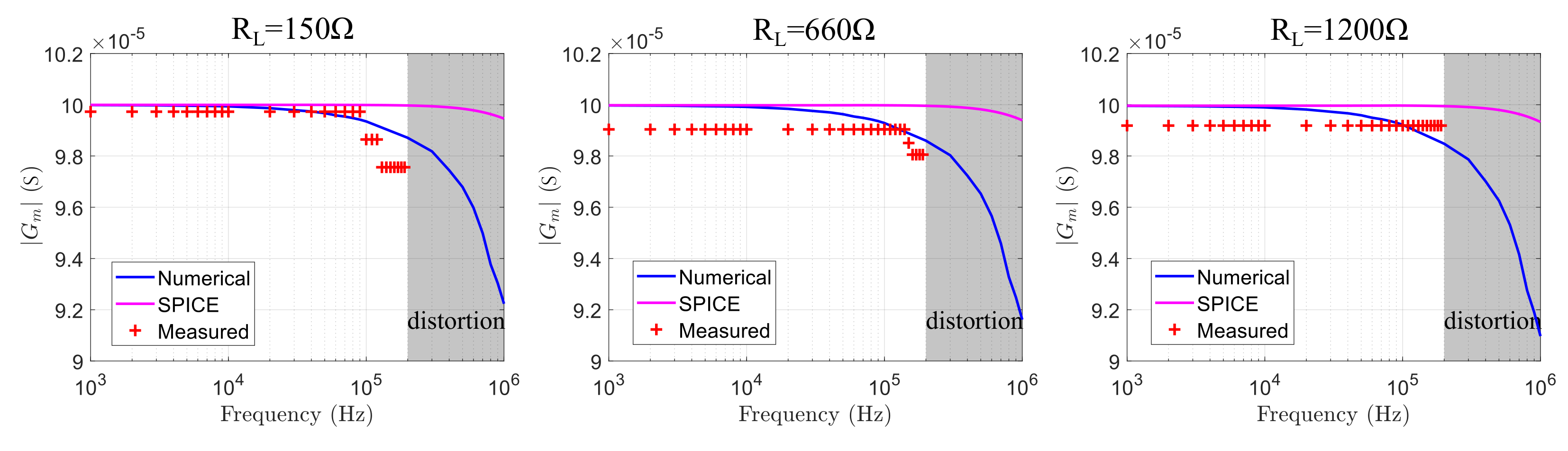
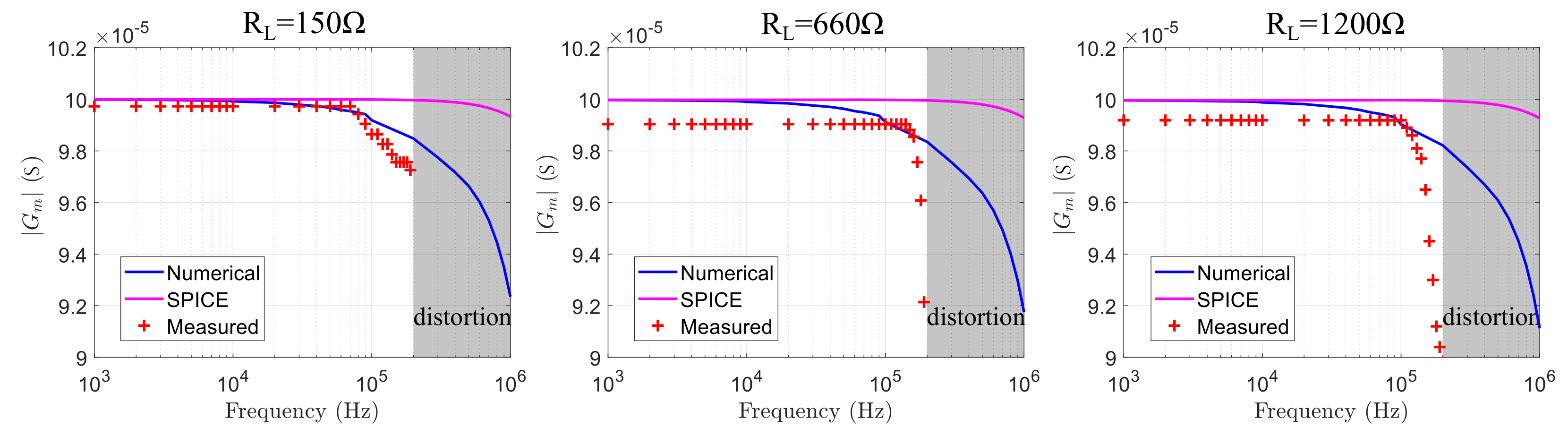
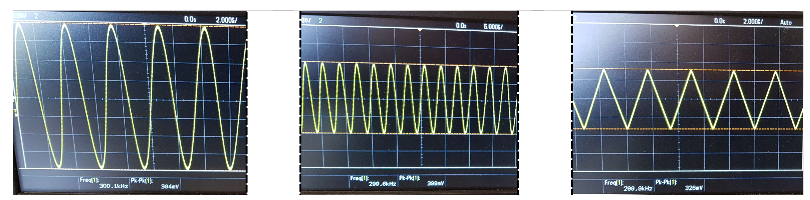
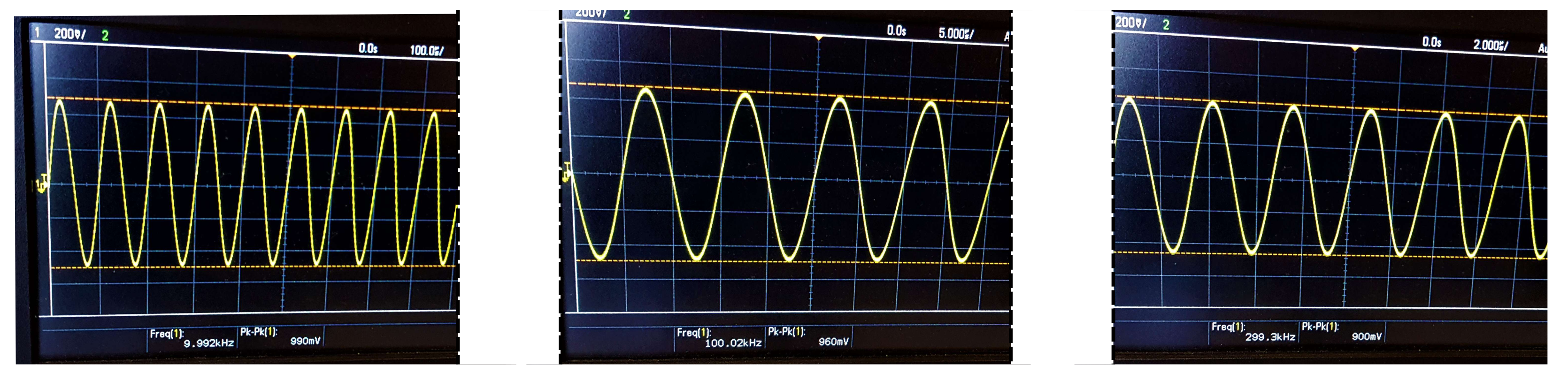
5. Implementation and Measurement Results
6. Conclusions
Author Contributions
Funding
Conflicts of Interest
References
- Gabriel, S.; Gabriel, C.; Corthout, E. The dielectric properties of biological tissues: I. Literature survey. Phys. Med. Biol. 1996, 68, 2231. [Google Scholar] [CrossRef] [Green Version]
- Gabriel, S.; Lau, R.; Gabriel, C. The dielectric properties of biological tissues: II. Measurements in the frequency range 10 Hz to 20 GHz. Phys. Med. Biol. 1996, 41, 2251. [Google Scholar] [CrossRef] [PubMed] [Green Version]
- Gabriel, S.; Lau, R.; Gabriel, C. The dielectric properties of biological tissues: III. parametric models for the dielectric spectrum of tissues. Phys. Med. Biol. 1996, 41, 2271. [Google Scholar] [CrossRef] [Green Version]
- Ibrahim, B.; Jafari, R. Cuffless blood pressure monitoring from an array of wrist bio-impedance sensors using subject-specific regression models: Proof of concept. IEEE Trans. Biomed. Circuits Syst. 2019, 13, 1723–1735. [Google Scholar] [CrossRef] [PubMed]
- Ibrahim, B.; Hall, D.A.; Jafari, R. Bio-impedance simulation platform using 3D time-varying impedance grid for arterial pulse wave modeling. In Proceedings of the 2019 IEEE Biomedical Circuits and Systems Conference (BioCAS), Nara, Japan, 17–19 October 2019. [Google Scholar]
- Ibrahim, B.; Hall, D.A.; Jafari, R. Pulse Wave Modeling Using Bio-Impedance Simulation Platform Based on a 3D Time-Varying Circuit Model. IEEE Trans. Biomed. Circuits Syst. 2021, 15, 143–158. [Google Scholar] [CrossRef]
- Wu, Y.; Hanzaee, F.F.; Jiang, D.; Bayford, R.H.; Demosthenous, A. Electrical Impedance Tomography for Biomedical Applications: Circuits and Systems Review. IEEE Open J. Circuits Syst. 2021, 2, 380–397. [Google Scholar] [CrossRef]
- Padilha Leitzke, J.; Zangl, H. A review on electrical impedance tomography spectroscopy. Sensors 2020, 20, 5160. [Google Scholar] [CrossRef]
- Takhti, M.; Odame, K. Structured design methodology to achieve a high SNR electrical impedance tomography. IEEE Trans. Biomed. Circuits Syst. 2019, 13, 364–375. [Google Scholar] [CrossRef]
- XMurphy, E.K.; Takhti, M.; Skinner, J.; Halter, R.J.; Odame, K. Signal-to-noise ratio analysis of a phase-sensitive voltmeter for electrical impedance tomography. IEEE Trans. Biomed. Circuits Syst. 2016, 11, 360–369. [Google Scholar] [CrossRef] [PubMed]
- Wu, Y.; Jiang, D.; Bardill, A.; De Gelidi, S.; Bayford, R.; Demosthenous, A. A high frame rate wearable EIT system using active electrode ASICs for lung respiration and heart rate monitoring. IEEE Trans. Circuits Syst. I Regul. Pap. 2018, 65, 3810–3820. [Google Scholar] [CrossRef]
- Rao, A.; Teng, Y.C.; Schaef, C.; Murphy, E.K.; Arshad, S.; Halter, R.J.; Odame, K. An analog front end ASIC for cardiac electrical impedance tomography. IEEE Trans. Biomed. Circuits Syst. 2018, 12, 729–738. [Google Scholar] [CrossRef]
- Takhti, M.; Odame, K. A power adaptive, 1.22-pW/Hz, 10-MHz read-out front-end for bio-impedance measurement. IEEE Trans. Biomed. Circuits Syst. 2019, 13, 725–734. [Google Scholar] [CrossRef]
- Bouchaala, D.; Kanoun, O.; Derbel, N. High accurate and wideband current excitation for bioimpedance health monitoring systems. Measurement 2016, 79, 339–348. [Google Scholar] [CrossRef]
- Bertemes-Filho, P.; Brown, B.H.; Wilson, A.J. A comparison of modified Howland circuits as current generators with current mirror type circuits. Physiol. Meas. 2018, 21, 1. [Google Scholar] [CrossRef] [Green Version]
- Hong, H.; Rahal, M.; Demosthenous, A.; Bayford, R.H. Comparison of a new integrated current source with the modified Howland circuit for EIT applications. Physiol. Meas. 2009, 30, 10999. [Google Scholar] [CrossRef]
- Bertemes-Filho, P.; Vincence, V.C.; Santos, M.M.; Zanatta, I.X. Low power current sources for bioimpedance measurements: A comparison between Howland and OTA-based CMOS circuits. J. Electr. Bioimpedance 2012, 3, 66–73. [Google Scholar] [CrossRef] [Green Version]
- Bertemes-Filho, P.; Felipe, A.; Vincence, V.C. High Accurate Howland Current Source: Output Constraints Analysis. Circuits Syst. 2013, 4, 451. [Google Scholar] [CrossRef] [Green Version]
- Batista, D.S.; Silva, G.B.; Granziera, F.; Tosin, M.C.; Gazzoni, D.L.; Melo, L.F. Howland Current Source Applied to Magnetic Field Generation in a Tri-Axial Helmholtz Coil. IEEE Access 2019, 7, 125649–125661. [Google Scholar] [CrossRef]
- Bouchaala, D.; Shi, Q.; Chen, X.; Kanoun, O.; Derbel, N. Comparative study of voltage controlled current sources for biompedance measurements. In Proceedings of the IEEE 2012 9th International Multi-Conference on Systems, Signals and Devices, Chemnitz, Germany, 20–23 March 2012; pp. 1–6. [Google Scholar] [CrossRef]
- Seoane, F.; Bragós, R.; Lindecrantz, K. Current source for multifrequency broadband electrical bioimpedance spectroscopy systems. A novel approach. In Proceedings of the IEEE 2006 9th International Conference of the IEEE Engineering in Medicine and Biology Society (EMBC), New York, NY, USA, 30 August–3 September 2006; pp. 5121–5125. [Google Scholar] [CrossRef]
- Zhang, F.; Teng, Z.; Zhong, H.; Yang, Y.; Li, J.; Sang, J. Wideband mirrored current source design based on differential difference amplifier for electrical bioimpedance spectroscopy. Biomed. Phys. Eng. Express 2018, 4, 025032. [Google Scholar] [CrossRef]
- Constantinou, L.; Triantis, I.F.; Bayford, R.; Demosthenous, A. High-power CMOS current driver with accurate transconductance for electrical impedance tomography. IEEE Trans. Biomed. Circuits Syst. 2014, 8, 575–583. [Google Scholar] [CrossRef]
- Constantinou, L.; Bayford, R.; Demosthenous, A. A wideband low-distortion CMOS current driver for tissue impedance analysis. IEEE Trans. Circuits Syst. II Express Briefs 2015, 62, 154–158. [Google Scholar] [CrossRef]
- Hong, H.; Rahal, M.; Demosthenous, A.; Bayford, R.H. Floating voltage-controlled current sources for electrical impedance tomography. In Proceedings of the 18th European Conference on Circuit Theory and Design, Seville, Spain, 27–30 August 2007; pp. 208–211. [Google Scholar] [CrossRef]
- Wu, Y.; Jiang, D.; Langlois, P.; Bayford, R.; Demosthenous, A. A CMOS current driver with built-in common-mode signal reduction capability for EIT. In Proceedings of the 43rd IEEE European Solid State Circuits Conference (ESSCIRC), Leuven, Belgium, 11–14 September 2017; pp. 227–230. [Google Scholar] [CrossRef]
- Bragos, R.; Rosell, J.; Riu, P. A wide-band AC-coupled current source for electrical impedance tomography. Physiol. Meas. 1994, 15, 91. [Google Scholar] [CrossRef]
- Rao, A.J.; Murphy, E.K.; Shahghasemi, M.; Odame, K.M. Current-conveyor-based wide-band current driver for electrical impedance tomography. Physiol. Meas. 2019, 40, 034005. [Google Scholar] [CrossRef] [Green Version]
- Texas, I. An-1515 a comprehensive study of the Howland current pump. In Application Report SNOA474A; Texas Instruments: Dallas, TX, USA, 2008. [Google Scholar]
- Filho, P.B. Tissue Characterization Using Impedance Spectroscopy Probe. Ph.D. Thesis, University of Sheffield, Sheffield, UK, 2002. [Google Scholar]
- Nouri, H.; Ayed, E.B.; Bouchaala, D.; Derbel, H.B.J.; Kanoun, O. Comparative Study of Howland Current Source Configurations for Accurate Biomedical Devices. In Proceedings of the IEEE 2019 5th International Conference on Nanotechnology for Instrumentation and Measurement (NanofIM), Sfax, Tunisia, 30–31 October 2019; pp. 1–8. [Google Scholar] [CrossRef]
- Mahnam, A.; Yazdanian, H.; Samani, M.M. Comprehensive study of Howland circuit with non-ideal components to design high performance current pumps. Measurement 2016, 82, 94–104. [Google Scholar] [CrossRef]
- Tucker, A.S.; Fox, R.M.; Sadleir, R.J. Biocompatible, high precision, wideband, improved Howland current source with lead-lag compensation. IEEE Trans. Biomed. Circuits Syst. 2012, 7, 63–70. [Google Scholar] [CrossRef] [PubMed]
- Morcelles, K.F.; Sirtoli, V.G.; Bertemes-Filho, P.; Vincence, V.C. Howland current source for high impedance load applications. Rev. Sci. Instruments 2017, 88, 114705. [Google Scholar] [CrossRef]
- Liu, J.; Qiao, X.; Wang, M.; Zhang, W.; Li, G.; Lin, L. The differential Howland current source with high signal to noise ratio for bioimpedance measurement system. Rev. Sci. Instruments 2014, 85, 055111. [Google Scholar] [CrossRef]
- Sirtoli, V.G.; Morcelles, K.F.; Vincence, V.C. Design of current sources for load common mode optimization. J. Electr. Bioimpedance 2018, 9, 59–71. [Google Scholar] [CrossRef] [Green Version]
- Shi, X.; Li, W.; You, F.; Huo, X.; Xu, C.; Ji, Z.; Dong, X. High-precision electrical impedance tomography data acquisition system for brain imaging. IEEE Sens. J. 2018, 18, 5974–5984. [Google Scholar] [CrossRef]
- Simini, F.; Bertemes-Filho, P. Bioimpedance in Biomedical Applications and Research; Springer: New York, NY, USA, 2018. [Google Scholar]
- Wi, H.; Sohal, H.; McEwan, A.L.; Woo, E.J.; Oh, T.I. Multi-frequency electrical impedance tomography system with automatic self-calibration for long-term monitoring. IEEE Trans. Biomed. Circuits Syst. 2013, 8, 119–128. [Google Scholar]
- Zarafshani, A.; Bach, T.; Chatwin, C.; Xiang, L.; Zheng, B. Current source enhancements in Electrical Impedance Spectroscopy (EIS) to cancel unwanted capacitive effects. Biomed. Appl. Mol. Struct. Funct. Imaging 2017, 10137, 101371X. [Google Scholar]
- Wu, Y.; Jiang, D.; Bardill, A.; Bayford, R.; Demosthenous, A. A 122 fps, 1 MHz bandwidth multi-frequency wearable EIT belt featuring novel active electrode architecture for neonatal thorax vital sign monitoring. IEEE Trans. Biomed. Circuits Syst. 2019, 13, 927–937. [Google Scholar] [CrossRef] [Green Version]
- Gaggero, P.O.; Adler, A.; Brunner, J.; Seitz, P. Electrical impedance tomography system based on active electrodes. Physiol. Meas. 2012, 33, 831. [Google Scholar] [CrossRef] [Green Version]
- Mellenthin, M.M.; Mueller, J.L.; De Camargo, E.D.L.B.; De Moura, F.S.; Santos, T.B.R.; Lima, R.G.; Alsaker, M. The ACE1 electrical impedance tomography system for thoracic imaging. IEEE Trans. Instrum. Meas. 2018, 68, 3137–3150. [Google Scholar] [CrossRef] [PubMed]
- Xu, J.; Mitra, S.; Matsumoto, A.; Patki, S.; Van Hoof, C.; Makinwa, K.A.; Yazicioglu, R.F. A wearable 8-channel active-electrode EEG/ETI acquisition system for body area networks. IEEE J. Solid-State Circuits 2014, 49, 2005–2016. [Google Scholar] [CrossRef] [Green Version]
- Alimisis, V.; Dimas, C.; Pappas, G.; Sotiriadis, P.P. Analog Realization of Fractional-Order Skin-Electrode Model for Tetrapolar Bio-Impedance Measurements. Technologies 2020, 8, 61. [Google Scholar] [CrossRef]
- Hanbin, M.; Su, Y.; Nathan, A. Cell constant studies of bipolar and tetrapolar electrode systems for impedance measurements. Sens. Actuators B Chem. 2015, 221, 1264–1270. [Google Scholar]
- Dimas, C.; Tsampas, P.; Ouzounoglou, N.; Sotiriadis, P.P. Development of a modular 64-electrodes electrical impedance tomography system. In Proceedings of the 2017 6th International Conference on Modern Circuits and Systems Technologies (MOCAST), Thessaloniki, Greece, 4–6 May 2017; pp. 1–4. [Google Scholar] [CrossRef]
- Kassanos, P.; Seichepine, F.; Yang, G.Z. A Comparison of Front-End Amplifiers for Tetrapolar Bioimpedance Measurements. IEEE Trans. Instrum. Meas. 2020, 70, 1–14. [Google Scholar] [CrossRef]
- Dimas, C.; Uzunoglu, N.; Sotiriadis, P.P. A parametric EIT system spice simulation with phantom equivalent circuits. Technologies 2020, 8, 13. [Google Scholar] [CrossRef] [Green Version]
- Kassanos, P.; Ip, H.M.; Yang, G.Z. A tetrapolar bio-impedance sensing system for gastrointestinal tract monitoring. In Proceedings of the 2015 IEEE 12th International Conference on Wearable and Implantable Body Sensor Networks (BSN), Cambridge, MA, USA, 9–12 June 2015; pp. 1–6. [Google Scholar] [CrossRef]
- Sun, J. Noise analysis of a driven chain with improved Howland current source for electrical impedance tomography. Meas. Sci. Technol. 2021, 32, 095903. [Google Scholar]


| 1 k | 1 k | 1 k | 1 k | 100 k | 10 k | 10 M | 1 nF |
| Resource | Topology | Opamp | Tolerance | , 10 kHz | , 100 kHz | , 1 MHz |
|---|---|---|---|---|---|---|
| [15] | Enhanced HCP | Not Mentioned | 750 k–4.5 M | 670 k | 70 k | |
| [15] | CCII with AD844 | No Opamp | 2 M | 288 k–700 k | 70 k | |
| [18] | Enhanced HCP | OPA655 | 80 k–10 M | 80 k–2 M | 80 k–300 k | |
| [32] | Enhanced HCP | LM741 | 200 k | 10 k | 5 k | |
| [32] | Buffered HCP | LM741 | 300 k | 20 k | 7 k | |
| [32] | Bridge HCP | LM741 | 600 k | 35 k | 7 k | |
| [32] | Enhanced HCP (pF ) | AD818 | 3 M | 200 k | 60 k | |
| [34] | Enhanced-Optimized Difference Evolution | AD825 | 5 M | 3 M | 100 k | |
| This Work | Mirrored-Buffered HCP- Active Electrode | AD8034 | 2.5 M–4 M | 0.9 M–2 M | 100 k–250 k |
| Test Case | Expected | Measured | Error (%) |
|---|---|---|---|
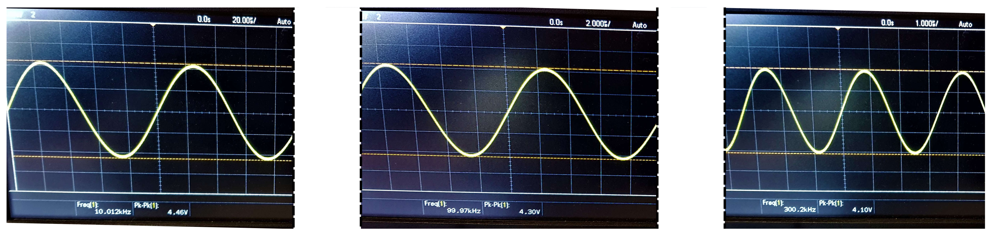
| 150 , kHz | 1014 | 990 | 2.36 |
| 150 , kHz | 1014 | 960 | 5.36 |
| 150 , kHz | 1014 | 900 | 11.2 |
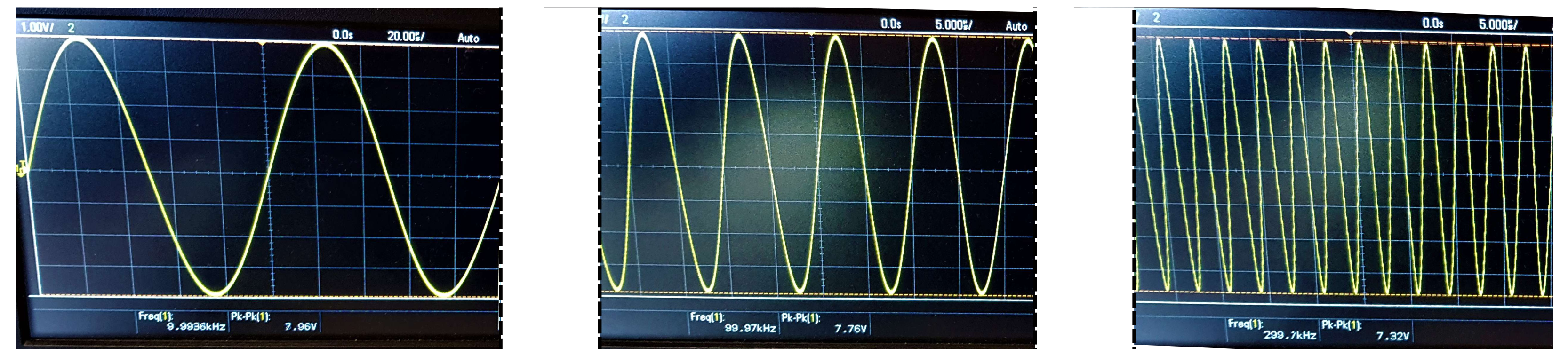
| 660 , kHz | 4465 | 4460 | 0.11 |
| 660 , kHz | 4465 | 4300 | 3.70 |
| 660 , kHz | 4465 | 4100 | 8.17 |
| 1200 , kHz | 8118 | 7960 | 1.94 |
| 1200 , kHz | 8118 | 7760 | 4.41 |
| 1200 , kHz | 8118 | 7320 | 9.83 |
Publisher’s Note: MDPI stays neutral with regard to jurisdictional claims in published maps and institutional affiliations. |
© 2021 by the authors. Licensee MDPI, Basel, Switzerland. This article is an open access article distributed under the terms and conditions of the Creative Commons Attribution (CC BY) license (https://creativecommons.org/licenses/by/4.0/).
Share and Cite
Dimas, C.; Alimisis, V.; Georgakopoulos, I.; Voudoukis, N.; Uzunoglu, N.; Sotiriadis, P.P. Analysis, Simulation, and Development of a Low-Cost Fully Active-Electrode Bioimpedance Measurement Module. Technologies 2021, 9, 59. https://0-doi-org.brum.beds.ac.uk/10.3390/technologies9030059
Dimas C, Alimisis V, Georgakopoulos I, Voudoukis N, Uzunoglu N, Sotiriadis PP. Analysis, Simulation, and Development of a Low-Cost Fully Active-Electrode Bioimpedance Measurement Module. Technologies. 2021; 9(3):59. https://0-doi-org.brum.beds.ac.uk/10.3390/technologies9030059
Chicago/Turabian StyleDimas, Christos, Vassilis Alimisis, Ioannis Georgakopoulos, Nikolaos Voudoukis, Nikolaos Uzunoglu, and Paul P. Sotiriadis. 2021. "Analysis, Simulation, and Development of a Low-Cost Fully Active-Electrode Bioimpedance Measurement Module" Technologies 9, no. 3: 59. https://0-doi-org.brum.beds.ac.uk/10.3390/technologies9030059