Article

Improving the Detection Accuracy of an Ag/Au Bimetallic Surface Plasmon Resonance Biosensor Based on Graphene

Shanghai Key Laboratory of Modern Optics System, Engineering Research Center of Optical Instrument and System, School of Optical-Electrical and Computer Engineering, University of Shanghai for Science and Technology, 516 Jungong Rd, Shanghai 200093, China
*
Author to whom correspondence should be addressed.
Submission received: 1 December 2021 / Revised: 17 December 2021 / Accepted: 23 December 2021 / Published: 27 December 2021
(This article belongs to the Special Issue Chemical Sensors for Bio-Medical and Environmental Applications)

Abstract

:
A theoretical study was conducted with the aim of improving the detection accuracy of graphene-based surface plasmon resonance (SPR) biosensors. We studied the effect of applying a bias voltage to the sensor surface on its detection accuracy. The optimum thicknesses of silver and gold layers in the biosensor of 47 nm and 3 nm, respectively, were determined. Graphene layers deposited on these thin silver and gold films formed a sensor surface system, on which the surface plasmons were excited. The real and imaginary parts of the refractive index of graphene were controlled by the bias voltage. When the chemical potential was increased from 36 meV to 8 eV, the detection accuracy of the sensor was correspondingly increased by 213%.

1. Introduction

Surface plasmon (SPs) is the collective oscillation of free electrons on the interface between metal and medium, under the excitation of a transverse magnetic p polarization wave, which produces a surface plasmon wave (SPW). The incident light enters on the metal film from the prism at a certain angle, and the light is totally reflected at the interface between the prism and the metal. When total reflection occurs, the light waves are not all reflected back onto the prism. Instead, they pass through the interface between the prism and the metal and enter the metal for a short distance. The transmitted wave with exponential attenuation is called the evanescent wave. The total reflection evanescent wave matches the SPW wave vector, and the light energy is transferred to effectively excite the surface plasmon resonance (SPR) [1,2,3]. Compared with the traditional resistance sensors, SPR-based biosensors are not only immune to electromagnetic interference, but also cheap and easy to make. Therefore, SPR-based biosensors are attractive for use in the fields of biomolecular detection, pathological diagnosis, and biochemical markers identification.
Graphene is a two-dimensional sheet of graphite with a honeycomb lattice structure. Graphene has many favorable characteristics, such as low magnetoresistance, excellent carrier mobility, high optical transparency, and extensibility. Recently, graphene has been widely used in the field of optoelectronics and sensors. Using graphene as a detection layer can greatly improve the sensitivity of the SPR sensors. In the conventional Krestschmann-type SPR biosensor structure, a metal film is coated on one side of a prism to separate the sensing medium from the prism. Such films are usually made of precious metals, such as gold and silver, which support the propagation of SPs at visible light frequencies. However, biomolecules show low adsorption capacities for gold. This shortcoming limits the sensitivity of traditional SPR biosensors. In previous studies, Wu et al. used the ATR method to detect the change of refractive index caused by biomolecule adsorption on a sensor surface. They found that a sensor with graphene on its surface exhibited higher sensitivity than that of a sensor containing only metal on its surface [4]. Maharana et al. found that the detection accuracy of chalcogenide glass with a high refractive index was 16 times higher than that of silicon glass [5]. Anower and co-workers found that the addition of a graphene layer to the sensor improved its S, but decreased its detection accuracy [6]. This was caused by the larger imaginary part of the permittivity of the graphene layer and its damping effect. To improve the detection accuracy of their sensor, the same group added a WS2 layer that overcame the limitations of the graphene-based sensor [7]. Moreover, Maurya et al. raised the detection accuracy of graphene-based sensors by adding a silicon layer [8]. Mudgal et al. increased the detection accuracy of graphene-based sensors by adding BaTiO3 material [9]. Consequently, much work remains to be conducted to improve the detection accuracy of graphene-based SPR biosensors.
In this paper, we demonstrate a high detection accuracy sensor based on graphene and a double-metal Krestschmann-type SPR structure. The optimal thickness of a bimetallic sensor is obtained by comparing the performance of a monometallic sensor with that of a bimetallic sensor. A graphene layer is included in the sensor. Varying the chemical potential of graphene can not only induce a high detection accuracy, but can also improve the quality factor. Additionally, we use Ge20Ga5Sb10S65 (2S2G) glass as the substrate, which can also improve the detection accuracy. As a result, the designed SPR biosensor is able to improve the detection accuracy by 213%, and improve the quality factor from 29.79 to 93.33 RIU−1.

2. Simulation Method

2.1. Performance Evaluation Formula

It is well known that, for optical surface wave structures, SPR strongly depends on the refractive index of the environmental dielectric. A change in the refractive index of the environmental dielectric occurred and caused a resonance peak shift in different resonance angle; by monitoring the resonance angle, we can measure the environmental media. The effect can be utilized to construct different types of sensors whose performances are usually described by sensitivity expressed by ref. [10]:
S = Δ θ Δ n ,
where Δ θ is the small change in SPR angle corresponding to the small change of the environmental media, and Δ n is the refractive index of the environmental dielectric.
Detection accuracy indicates how accurately the angular position of the dip minimum in an SPR curve can be located. The sharper the SPR spectral curve, the higher the detection accuracy is. In this study, we define detection accuracy as the ratio of the shift of the resonance angle relative to the full width at half-maximum (FWHM) of the reflectance curve, which makes it a unitless parameter.
  D . A .   = Δ θ   FWHM   .
Quality factor is the ratio of the sensitivity to the FWHM of the reflectance curve. The unit of the quality factor is RIU−1.
  Q   = S   FWHM   .

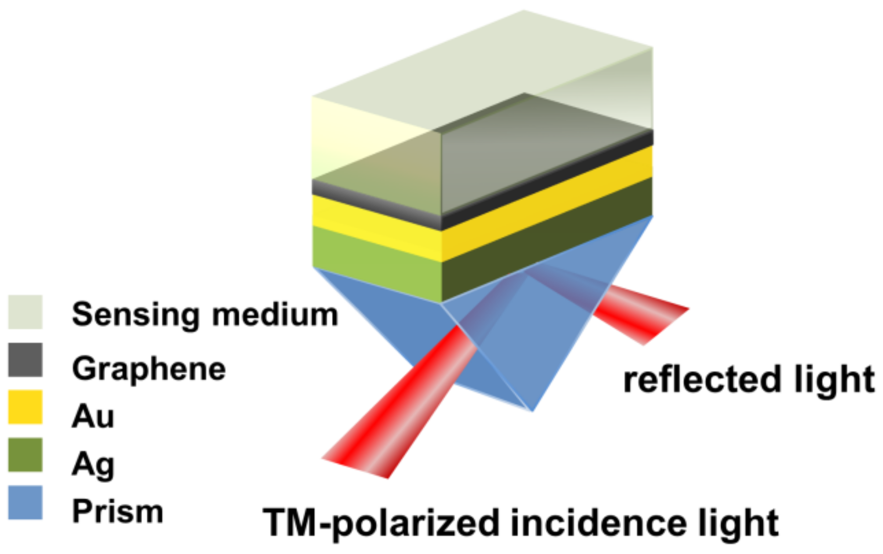
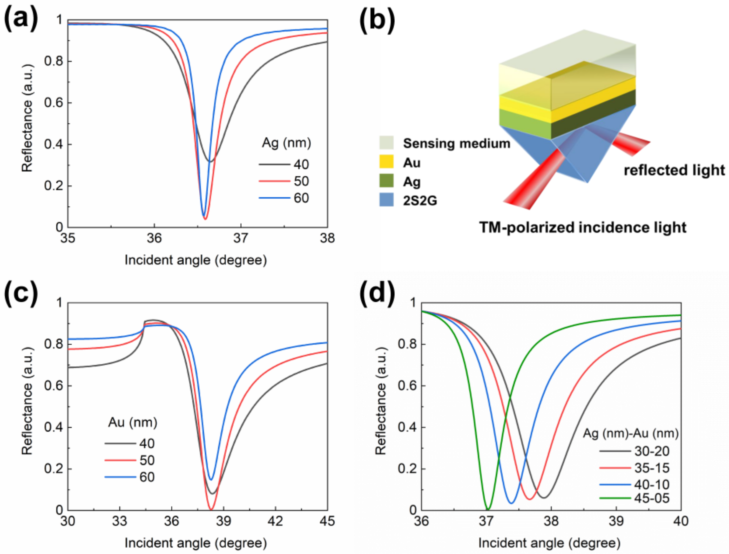
2.2. Sensor Structural Configuration

The structure of our proposed composite layered SPR sensor, which is based on the Kretschmann configuration, is shown in Figure 1. The first layer of the sensor is 2S2G glass, the second layer is Ag, the third layer is Au, the fourth layer is graphene, and the fifth layer is the sensing medium.
According to the principle of SPR, the refractive index of the prism material should be greater than that of the sample. Otherwise, there will be neither light coupling nor SPR. Silicon-based prisms are suitable for SPR measurements in the visible light range, while chalcogenide glasses have a wide operating window in the infrared region, leading to a large detection depth and accurate measurement of the angle. The refractive index of 2S2G glass has been calculated by using the following expression from ref. [11]:
n 252 G = 2.24047 + 2.693 × 10 2 λ 2 + 8.08 × 10 3 λ 4 .
The most common metal used in SPR sensor applications is Au because it has great environmental durability. Ag is also a good candidate for SPR chips, and its reflectance curve has a narrower FWHM and sharper dip, leading to higher detection accuracy. However, SPR sensors with only an Au layer provide high sensitivity with low of detection accuracy and quality factor, while that with only an Ag film ameliorates the sensor’s detection accuracy and quality factor at a cost of low sensitivity. Therefore, bimetallic structures consisting of Ag/Au films are considered as a compromise between two single metal based sensors [12,13,14,15,16,17].
In the calculation, the refractive index for Ag ( n Ag ) is taken as:
n Ag = 0.0562 + i 4.2760 .
In the calculation, the refractive index for Au ( n Au ) is taken from ref. [18]:
n Au = 0.1958 + i 3.2578 .
The real and imaginary parts of the metal refractive index control the transparency feature of the metal film. Furthermore, the real and imaginary parts become larger at longer wavelengths. Hence, we know that increasing the real part of the refractive index makes the metal more reflective from the prism–metal interface, whereas increasing the imaginary part makes it more absorptive.
The refractive index of graphene in the structure is calculated by the Kubo formula. The refractive index of the sensing medium layer is given as n s = 1.33 + Δ n , where Δ n is the index change of the sensing medium layer.

3. Simulation Results

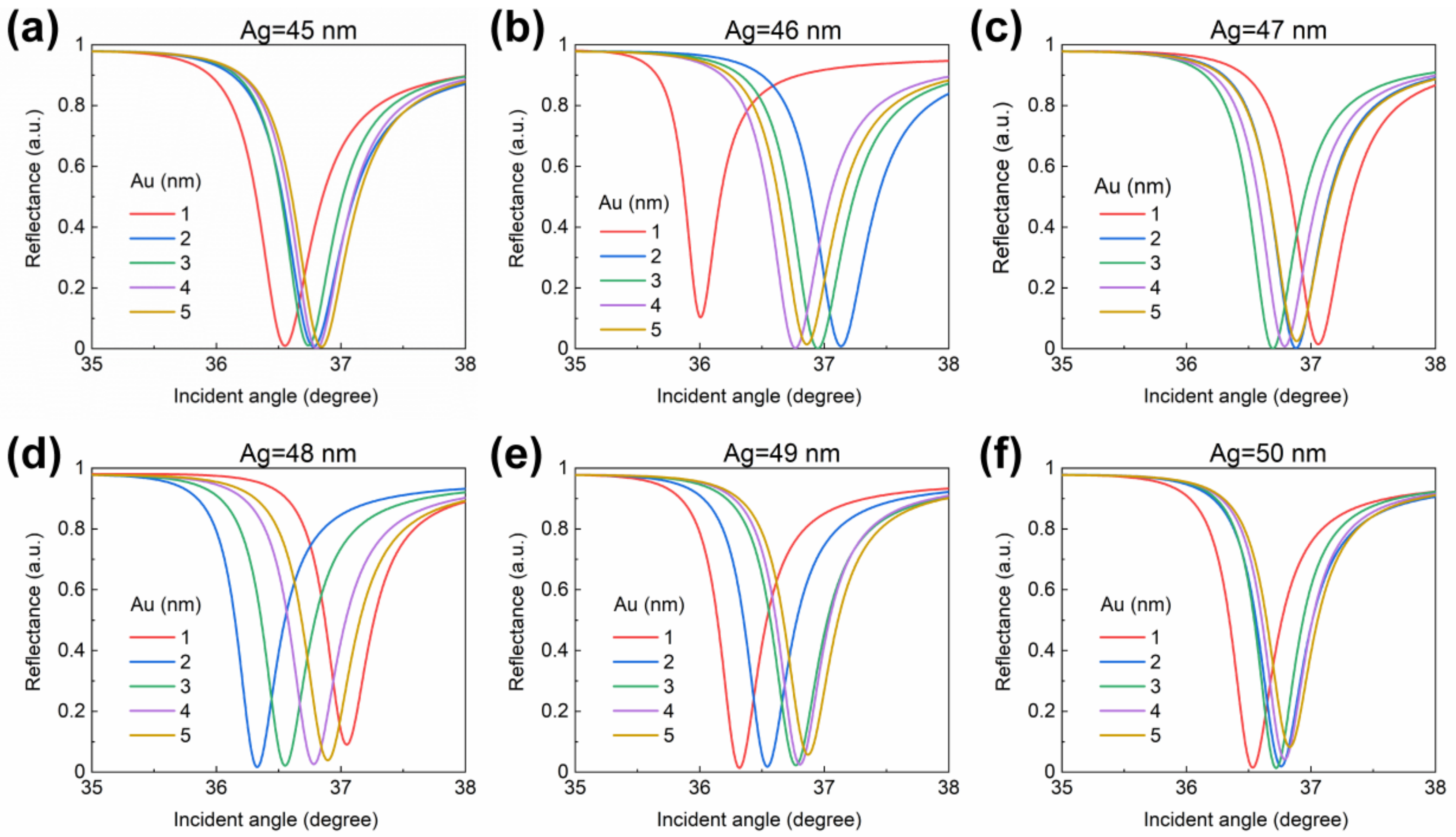
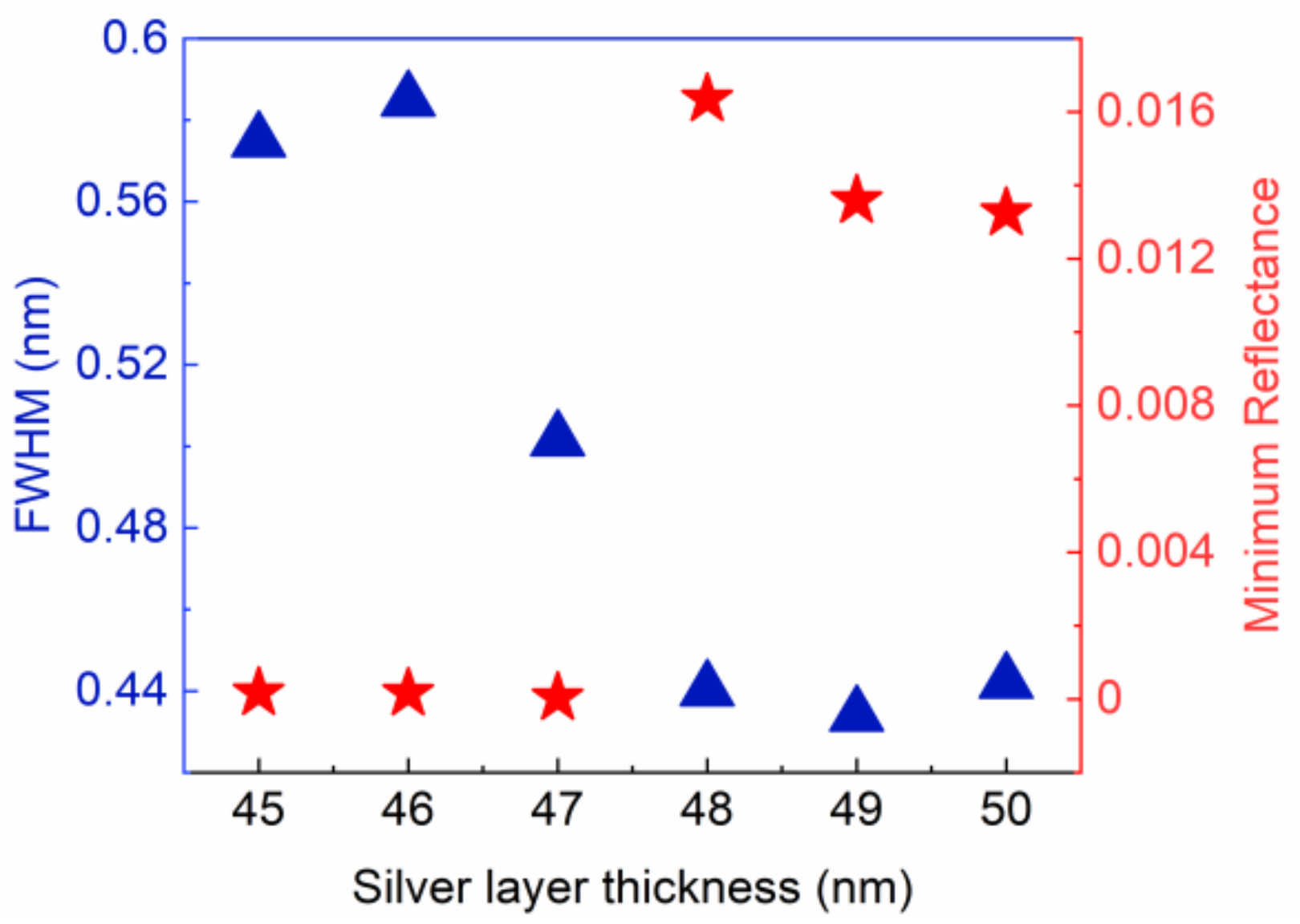
3.1. Influence of Metal Layer Thickness on SPR Spectral Curve

Silver and gold layers were used to study the reflectance of the sensor. The metal thickness was changed with an increment of 10 nm. There is clear evidence that zero reflection cannot be achieved, if the metal layer was thinner or thicker than the optimum thickness. If the metal layer was too thin, the SPPs were strongly damped due to the radiation damping in the glass. Conversely, if the metal film was too thick, SPPs were not effectively excited due to absorption by the metal. In biosensor applications, the surface properties of adsorbed biomolecules play an important role in determining the performance of biosensors. Gold has poor adsorption for biomolecules, which influences the performance of traditional SPR biosensors. A self-assembled monolayer (SAM) on the gold surface, generally by alkanothiols or disulfides, is one way to solve the limitation [19,20]. Such alkanethiols can be functionalized at the outer end of the molecule, and the functionalization is chosen so as to promote the interaction with further layers of biomolecules or other species. Another attractive alternative to improve the performance of SPR biosensors is to functionalize the gold film with biomolecular recognition elements (BRE), in order to enhance the adsorption of biomolecules on the gold surface. Graphene can act as a BRE on Au due to its carbon-based ring structure, which improves the sensitivity of biosensors [5,21,22].
We use FDTD solutions (commercial software) to simulate the structure. The sensor was illuminated with a plane wave source at the wavelength of 633 nm wavelength. Parameter sweep was used for angular interrogation over a wide range of source angels, in order to obtain the resonance angle. The parameter sweep was set up to run 400 times simulations at the angle range.
A structure reflection diagram of devices with a total Ag/Au thickness of 50 nm was drawn, in Figure 2d. However, it was difficult to determine the optimum thickness of the silver and gold layers from Figure 2. To solve this challenge, we calculated reflectance maps corresponding to the more accurate Ag and Au thicknesses. The thickness of the silver layer was increased from 45 nm to 50 nm, and that of the gold layer was increased from 1 nm to 5 nm, with an interval of 1 nm. The simulated change of reflectance at different incident angles with the thickness of the silver layer fixed, and the thickness of the gold layer changing, is shown in Figure 3. Table 1 lists the optimal thickness of the gold layer for silver layers with different thicknesses. The thicknesses of the Ag-Au layers are expressed as 45 nm-4 nm; 46 nm-3 nm; 47 nm-3 nm; 48 nm-2 nm; 49 nm-1 nm; and 50 nm-3 nm, respectively. The optimal thickness of the Au layer was 3 nm, when the Ag layer had a thickness of 47 nm.
The Rmin and FWHM of the gold layers, with an optimal thickness on different silver layers, are compared in Figure 4. It was found that Rmin decreased when the thickness of the silver layer was 47 nm or lower. The FWHM was narrower when the thickness of the silver layer was 48 nm or higher. When the thickness of the silver layer was 47 nm, it had both a low Rmin and narrow FWHM. Hence, an Ag layer with a thickness of 47 nm and an Au layer with a thickness of 3 nm were chosen in our sensors.

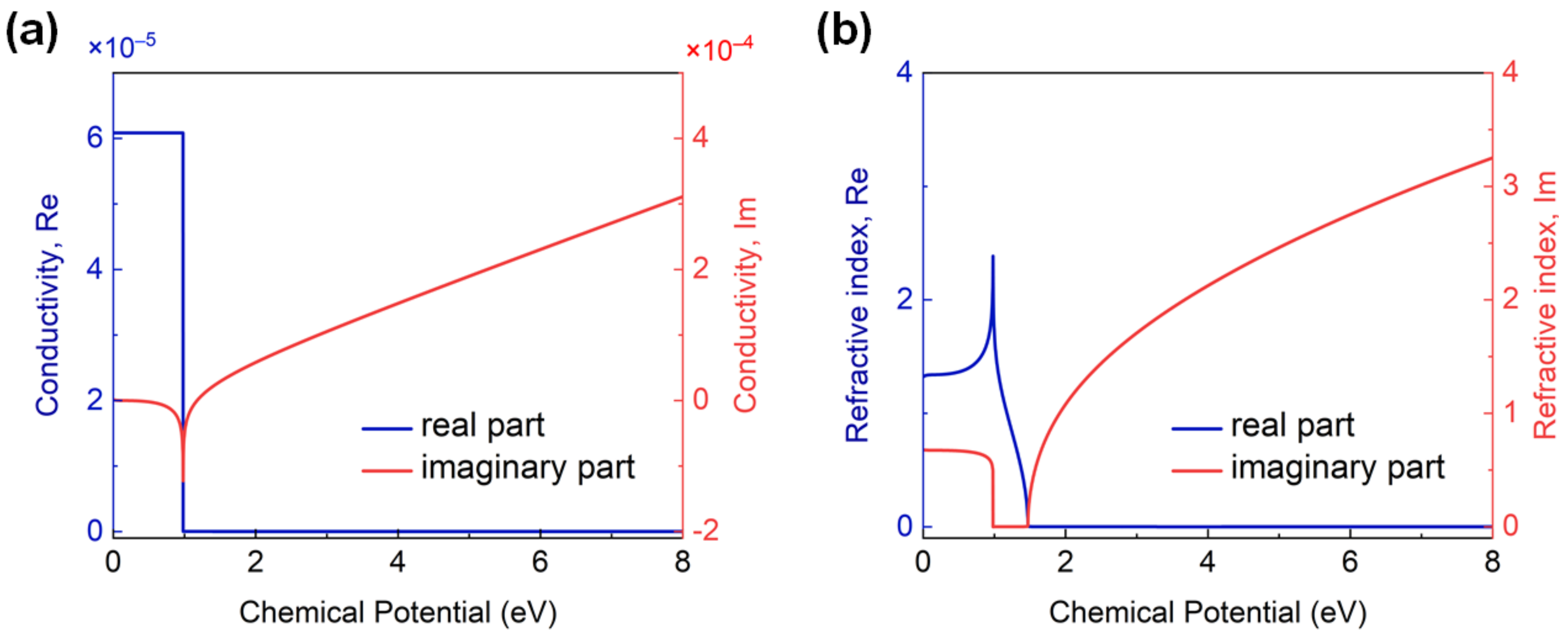
3.2. Effect of Chemical Potential on the Refractive Index of Graphene

Graphene is a thin two-dimensional layer of graphite, an allotrope of carbon, which contains carbon atoms arranged to form a honeycomb lattice structure [23]. The chemical potential of graphene can be easily moved above or below the Dirac point, which allows the carrier concentration ( n g ) of graphene to be adjusted by applying voltage. That, in our sensor, is the carrier concentration of graphene that can be determined by the applied voltage ( V g ) in Ref. [24]. n g is expressed by Equation (7).
n g = V g ε 0 ε r qd sub ,
where ε 0 = 8.85 × 10 12   F / m is the permittivity of the vacuum, ε r is the relative permittivity of the substrate, q is the electron charge, and d sub is the substrate thickness. Based on the carrier concentration of the system, the chemical potential μ c can be calculated from ref. [25]:
μ c = ћ v f π n g ,
where ћ = 1.055 × 10 34 J S is the reduced Planck’s constant and v f 10 6 m / s is the Fermi velocity. Graphene optical conductivity σ is related to the intra-band electron-photon scattering σ intra   and the inter-band electron transition conductivity σ inter   as a function of radiation frequency ω , and is given as the following equation.
σ ( ω ) = σ intra   ( ω ) + σ inter   ( ω ) ,
which can be calculated using the Kubo formula from ref. [26]:
σ intra   ( ω ) = i q 2 π ћ ω + i τ 1 × μ c + 2 K B T × ln exp μ c / K B T + 1 ,
σ inter   ( ω ) = i q 2 4 π ћ ln 2 μ c ћ ω + i τ 1 2 μ c + ћ ω + i τ 1 ,
where K B is the Boltzmann’s constant, T = 300   K is the temperature, τ = μ c m u / q v f 2 is the momentum relaxation time, m u = 10 4 cm 2 / V s is the impurity-limited direct current mobility, ω = 2 π c / λ is the angular frequency, and λ = 633   nm is the incident wavelength.
The complex conductivity of graphene can be expressed as:
σ ( ω ) = σ R ( ω ) + σ I ( ω ) ,
where σ R and σ I are the real and imaginary parts of the graphene conductivity.
If ћ ω > 2 μ c , then
σ R ( ω ) = π e 2 2 h = 6.085 × 10 5 ,
if ћ ω < 2 μ c , then
σ R ( ω ) = τ 1 q 2 π ћ 2 ω 2 + τ 2 × H ,
σ I ( ω ) = ω q 2 π ћ 2 ω 2 + τ 2 × H + q 2 4 π ћ ln 2 μ c ћ ω + i τ 1 2 μ c + ћ ω + i τ 1 ,
where H is the factor
H = μ c + 2 K B T × ln exp μ c / K B T + 1 .
The thickness of monolayer graphene is 0.34 nm, and for a given number of graphene layers with a thickness d G , the real n R and imaginary n I parts of the graphene refractive index can be calculated from ref. [27]:
n R 2 = σ I ω ε 0 d G 2 + σ R 2 1 / 2 σ I ω ε 0 d G 2 ω ε 0 d G ,
n I 2 = σ I ω ε 0 d G 2 + σ R 2 1 / 2 + σ I ω ε 0 d G 2 ω ε 0 d G .
By observing the conductivity and refractive index of the graphene layer, the effect of chemical potential can be discussed. The chemical potential of our sensor depends on the gate voltage [28].
As the number of graphene layers changes, the propagation constant of the surface plasmon wave shifts, which satisfies the resonance conditions at different angles [29]. The propagation constant is affected by the surface plasmon field extending to graphene, and the propagation speed of an electromagnetic wave in graphene is lower than that in the adjacent medium, resulting in a decrease in the propagation velocity of the surface plasmon wave and the damping. The stronger this effect, the greater the damping in the structure. Because the FWHM is a linear function of damping, both the detection accuracy and quality factor of a sensor decrease linearly with the increasing FWHM, which limits the number of graphene layers able to be included in high-quality sensors [30]. Furthermore, refs. [22,31] discuss the number of layers of the SPR sensor. They find that the best number of layers of graphene is three, so we used three layers of graphene in our sensor.
To ensure that our sensors had both high detection accuracy and quality factor, we used three graphene layers. Figure 5 shows the changes in the real and imaginary parts of the conductivity, and refractive index of the three-layer graphene when the chemical potential was varied from 64 meV to 8 eV.
The chemical potential of graphene and, therefore, its complex conductivity can be tuned by applying a bias voltage. As a result, graphene can behave like metal or dielectric, supporting TM and transverse electric (TE) surface waves, respectively [32]. As shown in Figure 5a, when ћ ω > 2 μ c , the imaginary part of surface conductivity is positive. In this case, the intra-band conductivity term dominates the surface conductivity of graphene and it will behave as an ultra-thin metal film supporting TM surface waves. Conversely, when 0 < μ c < ћ ω / 2 , the imaginary part of surface conductivity is negative. In this case, the inter-band conductivity is the dominant term and graphene will behave as a semiconductor. Figure 5a also indicates that for three-layer graphene when μ c is less than 0.98 eV; the real part of conductivity is a constant with a value of 6.085 × 10 5 . The imaginary part of conductivity gradually decreases. When μ c is greater than 0.98 eV, the real part of conductivity decreases to nearly zero, and the imaginary part of conductivity gradually increases. Figure 5b depicts the relationship between the graphene refractive index and chemical potential. According to the data in Figure 5b, the performance of the sensor under different graphene chemical potential can be calculated.

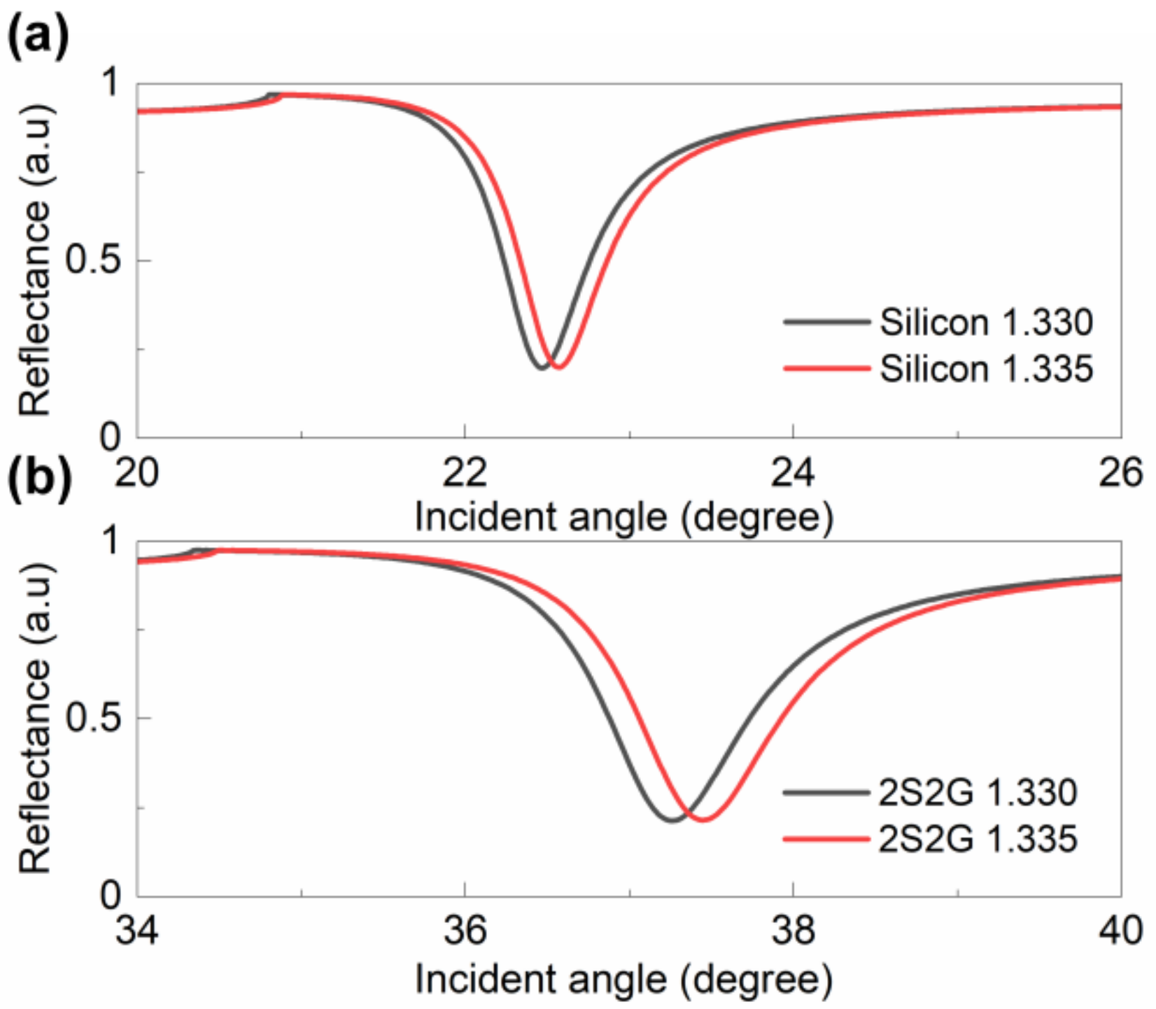
3.3. Influence of Substrates on the SPR Spectral Curve of the Proposed Sensor

According to the principle of plasmon resonance, the refractive index of the prism material should be greater than that of the sensing medium; otherwise, there will be neither light coupling nor plasmon resonance. We decided to compare the influence of different substrate materials on the sensitivity and detection accuracy of our proposed sensor. The substrates investigated were silicon [33] and 2S2G. The refractive index of 2S2G can be calculated from Equation (4). The refractive index of silicon can be calculated as follows:
n Silicon 2 = 11.6858 + 0.939816 λ 2 + 0.000993358 λ 2 1.22567 .
Figure 6 presents the shift of the resonance angle of our proposed sensor in the angular regime for two sensing media: water ( n = 1.330 ) and urine with a normal range of glucose concentration ( n = 1.335 ) [22]. Sensitivity of the sensor using silicon is 19.24 (°/RIU), and its detection accuracy is 0.1312. Sensitivity of the sensor, using 2S2G as the substrate, is 36.08 (°/RIU), and its detection accuracy is 0.1489. Therefore, to improve the detection accuracy of our sensor, we used 2S2G as the substrate material rather than silicon.

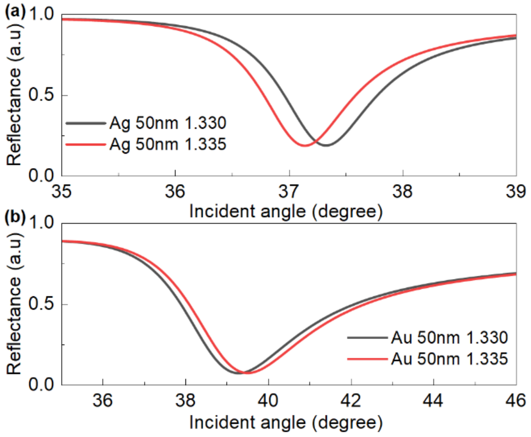
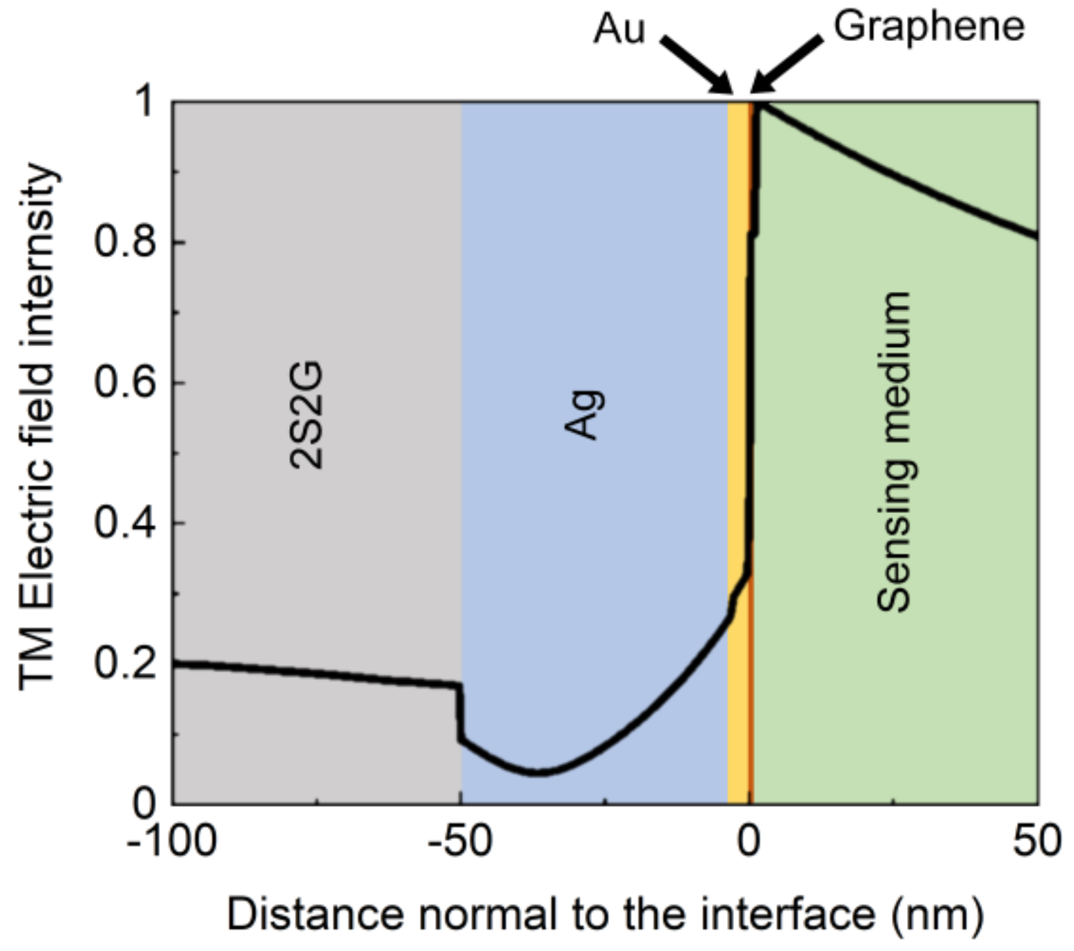
3.4. Benefits of the Bimetallic Configuration

The benefits of the bimetallic configuration can be realized by examining the performances of three configurations: having only an Ag layer, having only an Au layer, and having a coupled Ag/Au layer. Figure 7 shows the influence of single-layer Ag film and single-layer Au film on the reflection curve. The sensitivity of the sensor using Ag film is 31.66 (°/RIU), and its detection accuracy is 0.1421. The sensitivity of the sensor using Au film is 48.02 (°/RIU), and its detection accuracy is 0.0668. According to Figure 6b, the sensitivity of the Ag/Au sensor is 36.08 (°/RIU), and its detection accuracy is 0.1489.
The performance comparison of the sensor with single-layer metal and double-layer metal is shown in Table 2; a much better performance optical sensor can be achieved with the double-layer arrangement, compared to the single gold film SPR sensor.

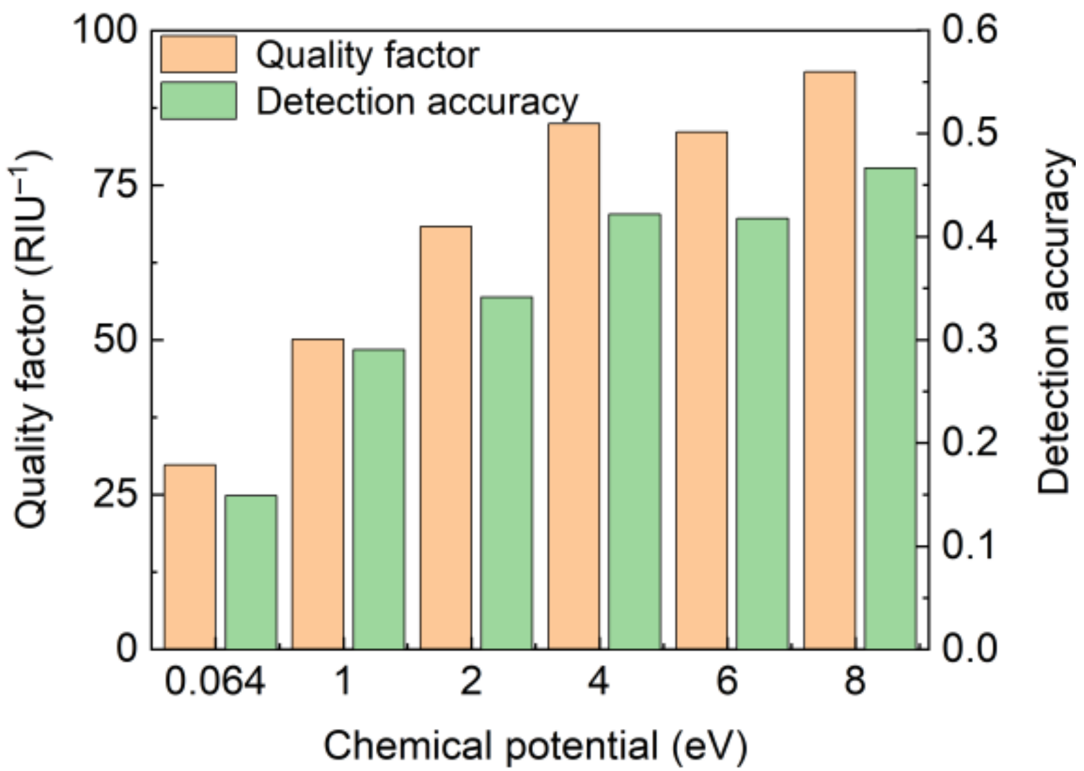
3.5. Effect of the Chemical Potential of Graphene on SPR Spectra

We observed that the surface conductivity of graphene changes with its chemical potential. Modifying the chemical potential of graphene changed its refractive index, which strongly affected the performance of the proposed SPR sensor. The incident wavelength of the sensor was 633 nm, the graphene layer number was 3, and the refractive index of the sensing medium was 1.330. Figure 8 shows the dependence of the SPR angle shift on chemical potential. When μ c was increased from 64 meV to 2 eV, the resonance angle increased. Conversely, the resonance angle decreased with the increase in μ c from 4 eV to 8 eV. The selection of Fermi energy, here, is referred to the ref. [27].
Table 3 shows the performance of the proposed sensor at different chemical potentials. Moreover, sensitivity, detection accuracy, and quality factors are defined by the previous Formulas (1) and (2). The increase in μ c had no obvious effect on sensitivity, but it affected the detection accuracy and quality factor. The detection accuracy of our proposed sensor was 0.1489 at 64 meV and 0.4666 at 8 eV. That is, detection accuracy increased by 213% by raising μ c . The quality factor increased from 29.79 to 93.33 RIU−1. Figure 9 illustrates the increase in the detection accuracy and quality factor with chemical potential. Our results show that applying a bias voltage to graphene can effectively improve the detection accuracy and quality factor of the sensors.
Table 4 compares the performance of the proposed SPR sensor with that of other reported sensors, including sensitivity and detection accuracy. Table 3 reveals that our proposed sensor has a higher detection accuracy than that of other sensors.
Finally, to better explain the performance of the proposed sensor, we simulated its normalized electric field intensity. The incident wavelength of the sensor was 633 nm, the graphene layers number was 3, and the refractive index of the sensing medium was 1.330. Figure 10 illustrates the normalized electric field intensity of the proposed sensor. The electric field strength of the metal film was enhanced after coating with graphene, which means that the SPRs were stronger.
Although we only study from the perspective of simulation, the feasibility of experimental method is also analyzed in the present study. Figure 11 is the schematic diagram of the experimental setup for the SPR sensor. Light is plunged with the wavelength of 633 nm from the laser source, the beam passes through a beam expander, a polarizer, and a half-wave plate, and reaches the SPR sensor. The TM-polarized light incidents from one lateral face of the prism, then reaches its base and totally reflected from the other lateral face. Computers and photodetectors are capable of measuring changes in the reflection, corresponding to changes in the refractive index. Samples with different refractive indexes can enter the encapsulated sensor surface from the sample channel with a syringe pump. The sensor is placed on the motorized rotation stage, and the incident angle is controlled by a motorized rotation stage, using computer.

4. Conclusions

In this work, we proposed an SPR sensor based on graphene and double-metal. The optimal thicknesses of the silver and gold layers in the sensor were determined to be 47 nm and 3 nm, respectively. The Kubo formula was used to calculate the refractive index of three-layer graphene at different Fermi energy. To improve the detection accuracy, the performance of sensors with different substrates was investigated. Changing the chemical potential of graphene modified its refractive index. We observed that the detection accuracy of the sensor was improved by 213%, by increasing the chemical potential. The proposed sensor potentially opens a new possibility for the biological detection of diabetes or diseases associated with liver and kidney dysfunction.

Author Contributions

All authors contributed to the study conception and design. Conceptualization, S.C. and Q.W.; methodology, S.C., X.G. and X.C.; software, S.C., X.G. and X.C.; writing—original draft preparation, S.C. and Q.W.; writing—review and editing, S.C. and Q.W.; supervision, D.Z.; project administration, Q.W. and D.Z. All authors have read and agreed to the published version of the manuscript.

Funding

This work was supported by the Shanghai Pujiang Program (No. 21PJD048) and the National Natural Science Foundation of China (No. 61775140, 62005165).

Conflicts of Interest

The authors declare no conflict of interest.

References

  1. Li, L.; Liang, Y.; Guang, J.; Cui, W.; Zhang, X.; Masson, J.; Peng, W. Dual Kretschmann and Otto configuration fiber surface plasmon resonance biosensor. Opt. Express 2017, 25, 26950–26956. [Google Scholar] [CrossRef] [PubMed]
  2. Wen, K.; Wei, S.; Shi, W. Thin-film tunable bandpass filter for spectral shift detection in surface plasmon resonance sensors. Opt. Lett. 2020, 45, 65–68. [Google Scholar] [CrossRef]
  3. Wang, J.; Lin, W.; Cao, E.; Xu, X.; Liang, W.; Zhang, X. Surface plasmon resonance sensors on Raman and fluorescence spectroscopy. Sensors 2017, 17, 2719. [Google Scholar] [CrossRef] [PubMed] [Green Version]
  4. Wu, L.; Chu, H.S.; Koh, W.S.; Li, E.P. Highly sensitive graphene biosensors based on surface plasmon resonance. Opt. Express 2010, 18, 15458–15463. [Google Scholar] [CrossRef]
  5. Maharana, P.K.; Jha, R. Chalcogenide prism and graphene multilayer based surface plasmon resonance affinity biosensor for high performance. Sens. Actuators B Chem. 2012, 169, 161–166. [Google Scholar] [CrossRef]
  6. Anower, M.S.; Rahman, M.S.; Rikta, K.A. Performance enhancement of graphene-coated surface plasmon resonance biosensor using tungsten disulfide. Opt. Eng. 2018, 57, 017114. [Google Scholar] [CrossRef]
  7. Rahman, M.S.; Hasan, R.; Akter, K.; Anower, M.S. A novel graphene coated surface plasmon resonance biosensor with tungsten disul fide (WS2) for sensing DNA hybridization. Opt. Mater. 2018, 75, 567–573. [Google Scholar] [CrossRef]
  8. Maurya, J.B.; Prajapati, Y.K.; Singh, V.; Saini, J.P.; Tripathi, R. Improved performance of the surface plasmon resonance biosensor based on graphene or MoS2 using silicon. Opt. Commun. 2016, 359, 426–434. [Google Scholar] [CrossRef]
  9. Mudgal, N. BaTiO3—Graphene-Affinity Layer—Based Surface Plasmon Resonance (SPR) Biosensor for Pseudomonas Bacterial Detection. Plasmonics 2020, 15, 1221–1229. [Google Scholar] [CrossRef]
  10. Jha, R.; Sharma, A.K. Chalcogenide glass prism based SPR sensor with Ag-Au bimetallic nanoparticle. J. Opt. A Pure Appl. Opt. 2009, 11, 045502. [Google Scholar] [CrossRef]
  11. Pandey, A.K.; Sharma, A.K.; Basu, R. On the Performance of Graphene based Plasmonic Biosensor with Bimetallic combination on 2S2G Prism. In Proceedings of the 2016 IEEE Annual India Conference (INDICON), Bangalore, India, 16–18 December 2016; Volume 2, pp. 3046–3052. [Google Scholar]
  12. Lee, H.S.; Seong, T.Y.; Kim, W.M.; Kim, I.; Hwang, G.W.; Lee, W.S.; Lee, K.S. Enhanced resolution of a surface plasmon resonance sensor detecting C-reactive protein via a bimetallic waveguide-coupled mode approach. Sens. Actuators B Chem. 2018, 266, 311–317. [Google Scholar] [CrossRef]
  13. Xia, L.; Yin, S.; Gao, H.; Deng, Q.; Du, C. Sensitivity Enhancement for Surface Plasmon Resonance Imaging Biosensor by Utilizing Gold-Silver Bimetallic Film Configuration. Plasmonics 2011, 6, 245–250. [Google Scholar] [CrossRef]
  14. Yuan, X.C.; Ong, B.H.; Tan, Y.G.; Zhang, D.W.; Irawan, R.; Tjin, S.C. Sensitivity-stability-optimized surface plasmon resonance sensing with double metal layers. J. Opt. A Pure Appl. Opt. 2006, 8, 959–963. [Google Scholar] [CrossRef]
  15. Dhibi, A.; Hakami, J.; Abassi, A. Performance analysis of surface plasmon resonance sensors using bimetallic alloy-perovskite-bimetallic alloy and perovskite-bimetallic alloy-perovskite nanostructures. Phys. Scr. 2021, 96, 065505. [Google Scholar] [CrossRef]
  16. Ong, B.H.; Yuan, X.; Tjin, S.C.; Zhang, J.; Ng, H.M. Optimised film thickness for maximum evanescent field enhancement of a bimetallic film surface plasmon resonance biosensor. Sens. Actuators B Chem. 2006, 114, 1028–1034. [Google Scholar] [CrossRef]
  17. Kashyap, R.; Chakraborty, S.; Zeng, S.; Swarnakar, S.; Kaur, S.; Doley, R.; Mondal, B. Enhanced biosensing activity of bimetallic surface plasmon resonance sensor. Photonics 2019, 6, 108. [Google Scholar] [CrossRef] [Green Version]
  18. Meshginqalam, B.; Barvestani, J. Aluminum and phosphorene based ultrasensitive SPR biosensor. Opt. Mater. 2018, 86, 119–125. [Google Scholar] [CrossRef]
  19. Llandro, J.; Palfreyman, J.J.; Ionescu, A.; Barnes, C.H.W. Magnetic biosensor technologies for medical applications: A review. Med. Biol. Eng. Comput. 2010, 48, 977–998. [Google Scholar] [CrossRef]
  20. Newton, L.; Slater, T.; Clark, N.; Vijayaraghavan, A. Self assembled monolayers (SAMs) on metallic surfaces (gold and graphene) for electronic applications. J. Mater. Chem. C 2013, 1, 376–393. [Google Scholar] [CrossRef]
  21. Lin, C.; Chen, S. Design of high-performance Au-Ag-dielectric-graphene based surface plasmon resonance biosensors using genetic algorithm. J. Appl. Phys. 2019, 125, 113101. [Google Scholar] [CrossRef]
  22. Maharana, P.K.; Jha, R.; Palei, S. Sensitivity enhancement by air mediated graphene multilayer based surface plasmon resonance biosensor for near infrared. Sens. Actuators B Chem. 2014, 190, 494–501. [Google Scholar] [CrossRef]
  23. Geim, A.K. Graphene: Status and Prospects. Science 2009, 324, 1530–1535. [Google Scholar] [CrossRef] [Green Version]
  24. Novoselov, K.S.; Geim, A.K. Electric Field Effect in Atomically Thin Carbon Films. Science 2004, 306, 666–670. [Google Scholar] [CrossRef] [Green Version]
  25. Thareja, V.; Kang, J.H.; Yuan, H.; Milaninia, K.M.; Hwang, H.Y.; Cui, Y.; Kik, P.G.; Brongersma, M.L. Electrically tunable coherent optical absorption in graphene with ion gel. Nano Lett. 2015, 15, 1570–1576. [Google Scholar] [CrossRef]
  26. Xiang, Y.; Guo, J.; Dai, X.; Wen, S.; Tang, D. Engineered surface Bloch waves in graphene-based hyperbolic metamaterials. Opt. Express 2014, 22, 3054–3062. [Google Scholar] [CrossRef]
  27. Gollapalli, R.P. Enhanced sensitivity in graphene-based SPR biosensors using electrical bias. Opt. Lett. 2020, 45, 2862–2865. [Google Scholar] [CrossRef]
  28. Soleymani, A.; Meymand, R.B. Broadband near-perfect terahertz absorber in single-layered and non-structured graphene loaded with dielectrics. Appl. Opt. 2020, 59, 2839–2848. [Google Scholar] [CrossRef]
  29. Mohanty, G.; Kumar, B.; Jamil, S. Comparative analysis for reflectivity of graphene based SPR biosensor. Opt. Quantum Electron. 2015, 47, 1911–1918. [Google Scholar] [CrossRef]
  30. Hossain, B.; Mustafa, I.; Moznuzzaman, M.; Faisal, L.; Hossain, A. High performance refractive index SPR sensor modeling employing graphene tri sheets. Results Phys. 2019, 15, 102719. [Google Scholar] [CrossRef]
  31. Ding, L.; Xu, C.; Xia, Z.; Xu, B.; Huang, J. Controlling polarization-dependent optical absorption of graphene through its thickness. Optik 2017, 137, 59–64. [Google Scholar] [CrossRef]
  32. Brahmachari, K.; Ray, M. Admittance loci based design of a nanobioplasmonic sensor and its performance analysis. Sens. Actuators B Chem. 2015, 208, 283–290. [Google Scholar] [CrossRef]
  33. Palik, E.D. Handbook of Optical Constants of Solids; Academic Press: Cambridge, MA, USA, 1985; Volume 1, ISBN 9780080547213. [Google Scholar]
  34. Xiang, Y.; Zhu, J.; Wu, L.; You, Q.; Ruan, B.; Dai, X. Highly Sensitive Terahertz Gas Sensor Based on Surface Plasmon Resonance with Graphene. IEEE Photonics J. 2018, 10, 6800507. [Google Scholar] [CrossRef]
  35. Banerjee, J.; Ray, M. Comparative performance evaluation of mono-metallic and bi-metallic plasmonic sensors using WS2 and graphene with optical bio-sensing application. Sens. Actuators B Chem. 2019, 281, 520–526. [Google Scholar] [CrossRef]
Figure 1. Schematic diagram of the proposed absorber.
Chemosensors 10 00010 g001
Figure 2. Surface plasmon resonance curves at a wavelength of 633 nm of sensors containing (a) an Ag film. (b) The structure of the SPR sensor based on the Kretschmann configuration. The refractive index of the sensing medium layer is 1.33. (c) an Au film, and (d) both Ag and Au films of different thicknesses.
Chemosensors 10 00010 g002
Figure 3. Reflectance of devices with the thicknesses of the silver layer at (a) 45 nm, (b) 46 nm, (c) 47 nm, (d) 48 nm, (e) 59 nm, and (f) 50 nm, and the gold layer as a different thickness. The refractive index of the sensing medium layer is 1.33.
Chemosensors 10 00010 g003
Figure 4. Optimal thicknesses of gold layers on silver layers with different thicknesses and corresponding Rmin (pentagram) and FWHM (trilateral).
Chemosensors 10 00010 g004
Figure 5. (a) Chemical potential (eV) versus conductivity and (b) chemical potential (eV) versus refractive index for three-layer graphene.
Chemosensors 10 00010 g005
Figure 6. Influence of (a) silicon and (b) 2S2G glass substrates on the reflectance spectra of the proposed sensor.
Chemosensors 10 00010 g006
Figure 7. Reflectance spectra of the SPR sensor with (a) single-layer Ag film and (b) single-layer Au film.
Chemosensors 10 00010 g007
Figure 8. Normalized reflectance of the proposed SPR sensor at different chemical potentials.
Chemosensors 10 00010 g008
Figure 9. Comparison of the quality factor and detection accuracy of the proposed sensor at different chemical potentials.
Chemosensors 10 00010 g009
Figure 10. Normalized electric field intensity of the proposed SPR sensor.
Chemosensors 10 00010 g010
Figure 11. Schematic diagram of the experimental setup for SPR sensor.
Chemosensors 10 00010 g011
Table 1. Optimal thicknesses of the gold layers on silver layers with different thicknesses, and corresponding Rmin and FWHM.
Thickness of Ag (nm)Thickness of Au (nm)RminFWHM
4540.00016609100.57477
4630.00015134700.58477
4730.00003288270.50143
4820.01634390000.44018
4910.01357580000.43395
5030.01323870000.44210
Table 2. Performance comparison of the sensor with single-layer metal and double-layer metal.
SPR Angle Shift (°)FWHMS (°/RIU)D.A.Q(RIU−1)
Ag (50 nm)0.15831.114331.660.142128.41
Au (50 nm)0.24013.592448.020.066813.37
Ag/Au (47 nm-3 nm)0.18041.211236.080.148929.79
Table 3. Performance of the SPR sensor at different chemical potentials.
Chemical Potential (eV)SPR Angle Shift (°)FWHMS (°/RIU)D.A.Q(RIU−1)
0.0640.18041.211236.080.148929.79
10.18040.621036.080.290550.10
20.20040.586640.080.341668.33
40.20040.471840.080.421784.95
60.18030.431836.080.417683.56
80.18040.386636.080.466693.33
Table 4. Comparison performance among the proposed sensor with that of other reported sensors.
ReferencesStructureS (°/RIU)D.A.
[5]2S2G/Au/Graphene460.181
[34]2S2G/air/Au/Graphene43.180.2641
[35]BK7/Ag/Au/WS2/Graphene1350.2956
Proposed work2S2G/Ag/Au/Graphene36.080.4666
Publisher’s Note: MDPI stays neutral with regard to jurisdictional claims in published maps and institutional affiliations.

