Article

Optical Response of CVD-Grown ML-WS2 Flakes on an Ultra-Dense Au NP Plasmonic Array

1
OptMatLab, Department of Physics, University of Genova, Via Dodecaneso 33, 16146 Genova, Italy
2
Center for Nanotechnology Innovation @NEST, Istituto Italiano di Tecnologia, Piazza San Silvestro 12, 56127 Pisa, Italy
3
Graphene Labs, Istituto Italiano di Tecnologia, Via Morego 30, 16163 Genova, Italy
4
Institute of Physics, Chemnitz University of Technology, Reichenhainer Str. 70, 09126 Chemnitz, Germany
5
Center for Materials, Architectures, and Integration of Nanomembranes (MAIN), Rosenbergstraße 6, 09126 Chemnitz, Germany
6
Consiglio Nazionale delle Ricerche—SuPerconducting and Other INnovative Materials and Devices Institute (CNR-SPIN), C.so Perrone 24, 16152 Genova, Italy
*
Authors to whom correspondence should be addressed.
Submission received: 30 December 2021 / Revised: 7 March 2022 / Accepted: 10 March 2022 / Published: 21 March 2022

Abstract

:
The combination of metallic nanostructures with two-dimensional transition metal dichalcogenides is an efficient way to make the optical properties of the latter more appealing for opto-electronic applications. In this work, we investigate the optical properties of monolayer WS 2 flakes grown by chemical vapour deposition and transferred onto a densely-packed array of plasmonic Au nanoparticles (NPs). The optical response was measured as a function of the thickness of a dielectric spacer intercalated between the two materials and of the system temperature, in the 75–350 K range. We show that a weak interaction is established between WS 2 and Au NPs, leading to temperature- and spacer-thickness-dependent coupling between the localized surface plasmon resonance of Au NPs and the WS 2 exciton. We suggest that the closely-packed morphology of the plasmonic array promotes a high confinement of the electromagnetic field in regions inaccessible by the WS 2 deposited on top. This allows the achievement of direct contact between WS 2 and Au while preserving a strong connotation of the properties of the two materials also in the hybrid system.

Graphical Abstract

1. Introduction

Among two-dimensional (2D) materials, transition metal dichalcogenides (TMDCs) arouse great interest due to the variety of physico-chemical properties they can offer [1,2,3,4]. Within the group-VI semiconducting TMDCs [5], such as Mo- and W-based sulphides and selenides, thinning down to the three-atom-thick monolayer (ML) leads to an indirect-to-direct bandgap transition [6,7]. Moreover, the energy gap at the two inequivalent K points of the hexagonal Brillouin zone falls in the visible-light range [8,9]. This makes TMDCs extremely intriguing light-sensitive materials for optoelectronics and photonics applications [8,10,11,12].
Within ML-TMDCs, an interesting consequence of the quantum confinement and the weak dielectric screening from the environment is the presence of tightly-bound excitons, characterized by binding energies in the order of hundreds of meV [13,14,15,16,17,18]. As a consequence, the optical properties of ML-TMDCs are governed by excitons even at room temperature [19,20].
For practical applications, however, ML-TMDCs exhibit a too weak optical absorbance. A viable strategy, thus, to increase their absorbance is represented by their integration with plasmonic nanostructures [21,22,23]. The electromagnetic-field (EM) confinement and amplification typical of metallic nano-objects supporting localized surface plasmon resonances (LSPR), i.e., light-induced collective electron oscillations [24,25], can indeed significantly strengthen the interaction of light with ML-TMDCs.
Due to the increasing interest in such hybrid systems, diverse solutions have been proposed for the integration of TMDC flakes with plasmonic materials. Depending on the application, both double-layer architectures and three-layer sandwich heterostructures were realized [26]. The first systems are composed of a layer of metallic nanostructures and a TMDC layer, while, in the latter, a TMDC flake is interposed between a continuous or nanostructured metal film and a layer of metallic nanostructures. Such hybrid architectures were exploited to increase the optical absorbance within ML-TMDCs and to control their PL properties [27,28,29,30,31,32].
The near-field interaction with plasmonic chiral metasurfaces also proved successful for the manipulation of TMDC valley-polarized PL [33], while photonic metasurfaces were used to control non-linear optical processes, e.g., second harmonic generation within 2D-TMDCs [34,35]. Another effective solution to manipulate optical, electronic and structural properties of ML-TMDCs is via the plasmon-induced hot electron injection from metallic nanostructures in contact with 2D semiconductors [36,37,38,39], which allows the control of TMDC exciton binding energy [36] and may lead to a significant bandgap renormalization [37].
Additionally, by using ad hoc designed hybrid architectures composed of few-layer and ML TMDCs integrated with plasmonic resonators, strongly-coupled excitonic-plasmonic systems were realized, with the possibility of achieving sizable Rabi-like energy splitting at low and even room temperature [40,41]. More in general, both the morphology and the geometry of the hybrid system strongly affects the plasmon–exciton coupling regime [42].
In this article, we address the optical response of ML-WS 2 laid on top of a densely-packed array of Au NPs, by means of micro-photoluminescence and micro-transmittance spectroscopies.
Ultra-dense arrays of metallic NPs are large-area plasmonic systems, which can be obtained by rather simple and cheap fabrication methods and exhibit tunable optical characteristics, exploitable for fundamental studies or plasmon-enhanced applications, such as SPR-enhanced optical spectroscopies or SPR-based sensing [43,44].
The WS 2 flakes were grown by chemical vapour deposition (CVD) and transferred onto the plasmonic substrate, where a thickness-graded ultra-thin insulating intercalation layer is present. We performed temperature-dependent studies in the 75–350 K temperature range of the hybrid system, unveiling the role of the thermal excitation and of the spacer layer thickness on the overall response.We concluded that the tight packing of the plasmonic particles, and the consequently limited EM-field spillout, promotes a weak interaction between the plasmonic and semiconducting sub-systems. The possibility to combine 2D TMDCs with densely-packed plasmonic arrays can make these systems promising, for example, in the field of molecular sensing [45,46].

2. Materials and Methods

2.1. Fabrication of the WS 2 /Au NPs Hybrid System

The plasmonic substrate is composed of a regular array of Au NPs on lithium fluoride (LiF) realized by depositing 3 nm of Au film onto a uniaxial pre-nanopatterned LiF (110) surface by molecular beam epitaxy under ultra-high vacuum conditions (p b a s e 10 9 mbar), and annealing the sample to induce solid-state dewetting of the thin film [47,48]. Since the LSPR depends on many parameters, we optimized the fabrication conditions of the Au NP array in order to match its LSPR energy to that of the WS 2 A exciton.
A thickness-graded LiF layer, with the thickness increasing from zero to about 10 nm over several millimeters, was then evaporated on top of the Au NPs at normal incidence.
WS 2 flakes were grown on SiO 2 /Si via liquid-precursor CVD (LqP-CVD) in a two-zone horizontal furnace (Lenton), following a procedure already detailed in previous studies [49,50,51]. Briefly, an aqueous solution containing a tungsten precursor (ammonium metatungstate hydrate, AMT, Sigma-Aldrich Inc, St. Luis, MO, USA, 463922) was mixed with an aqueous solution with the growth promoter (NaOH) and iodixanol, used as a density gradient (Sigma-Aldrich Inc., Opti Prep, D1556) and deionized water, in a ratio 1.5:2:1:2.
The final solution was spin-coated on a SiO 2 /Si substrate, previously cleaned via sonication in acetone and isopropanol for 5 min and treated with oxygen plasma [50]. During the growth, the spin-coated substrate was heated at high pressure at 800 C for 10 min under constant Ar/H 2 flux, while sulphur pellets were maintained at 180–210 C to induce their sublimation. At the end of the growth, the reactor was naturally cooled down under constant Ar flux.
The hybrid system was fabricated by transferring the as-grown WS 2 flakes onto the plasmonic substrate by means of a semidry transfer approach, following the same procedure described in previous works [52,53]. After the transfer, the flakes were randomly distributed on the sample surface, either in direct contact with the Au NPs or separated from them by the LiF spacer. A section of the sample was left bare, i.e., without Au NPs, in order to be able to probe WS 2 flakes directly deposited on the insulating substrate.

2.2. Variable-Temperature Transmittance Spectro-Microscopy

The samples were placed inside a cryostat with optical access (Optistat CF-V, Oxford Instruments plc, Tubney Woods, Abingdon, UK), in high vacuum conditions (p b a s e 10 6 mbar), and their temperature varied in the 75 to 350 K range. White light from a lamp, linearly polarized along the uniaxial LiF nanogrooves, impinged on the samples and, after transmission, was collected by a 5× long-working-distance objective and split in two beams. One of the beams was used for optical imaging, while the other beam was collimated by a pinhole and coupled to a spectrometer (AvaSpec-ULS2048XL-EVO, Avantes B. V., NS Apeldoorn, The Netherlands), allowing the measurement of transmittance spectra in the 400–800 nm wavelength range with a lateral resolution of approximately 20 μ m.

2.3. Photoluminescence Spectro-Microscopy
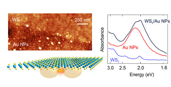
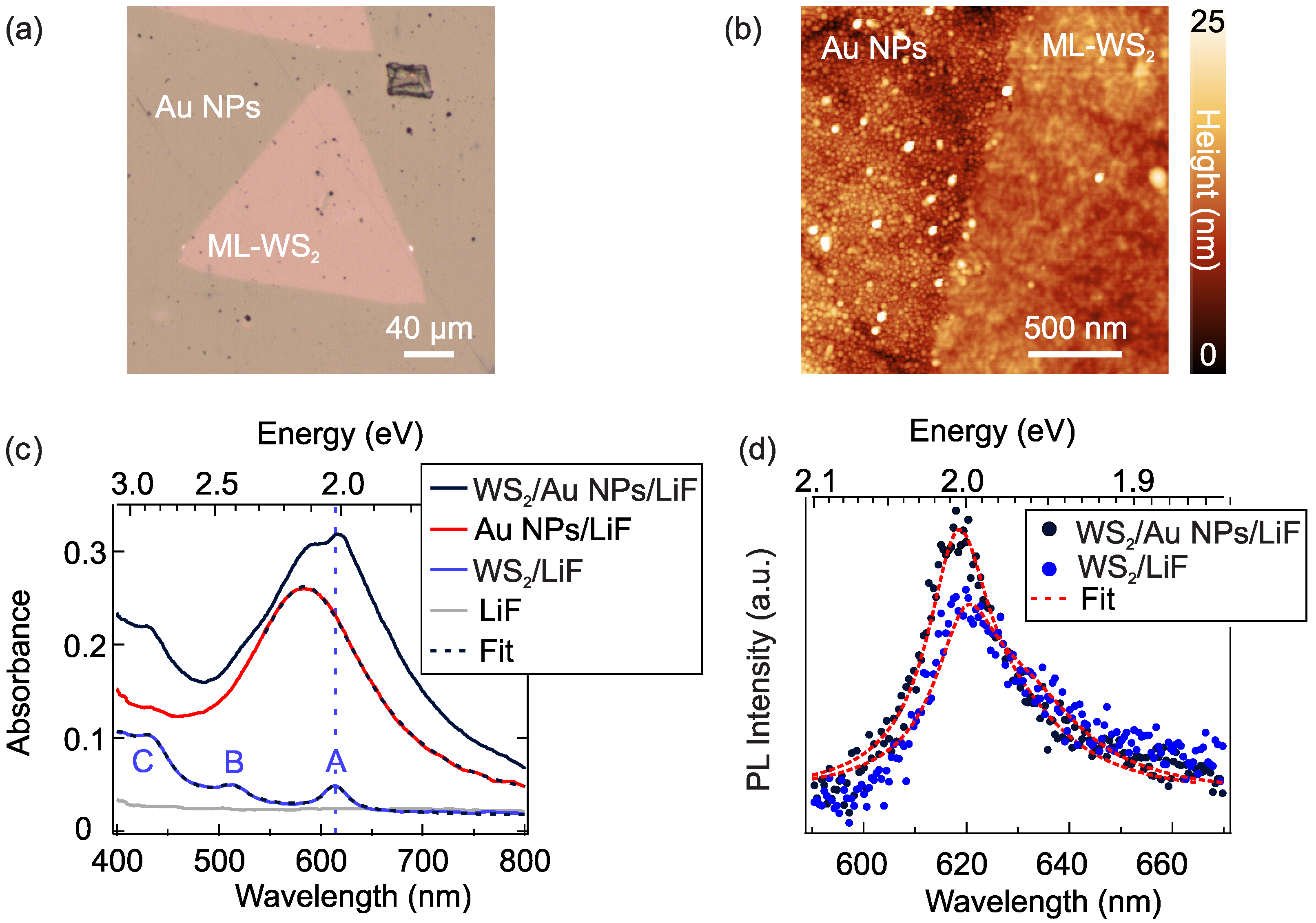
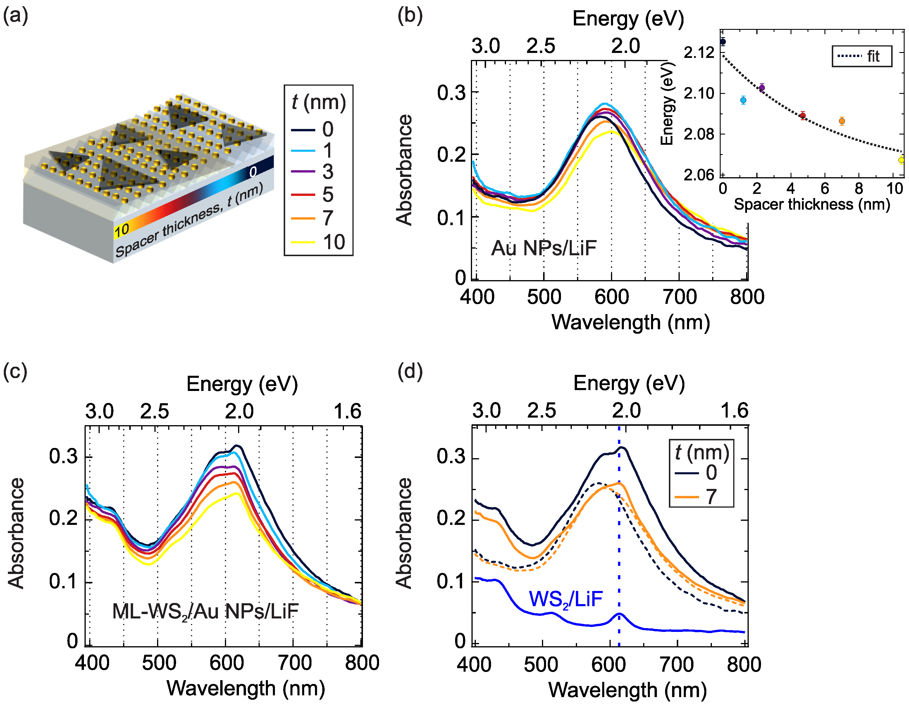
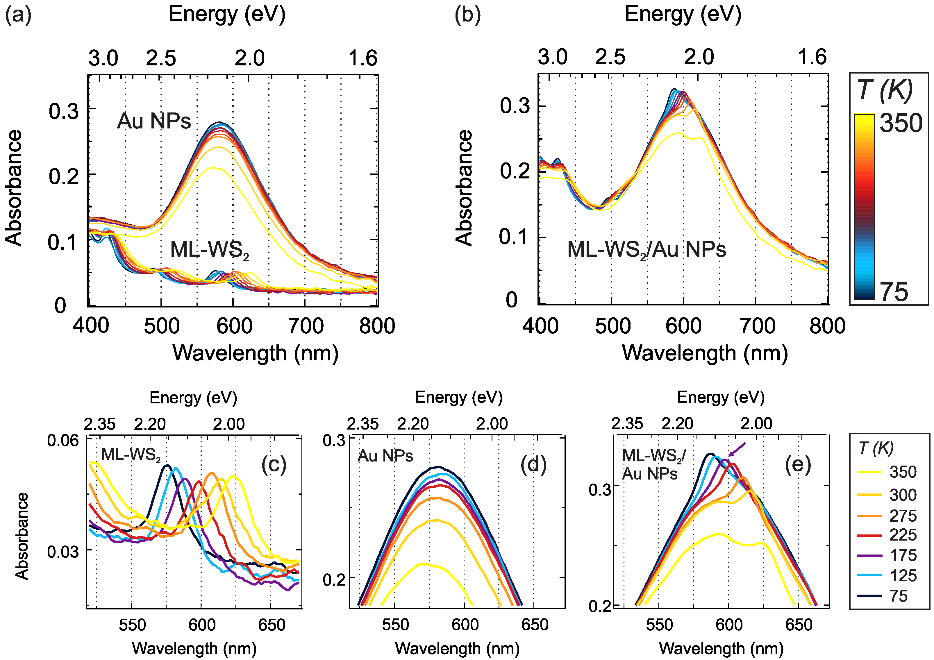
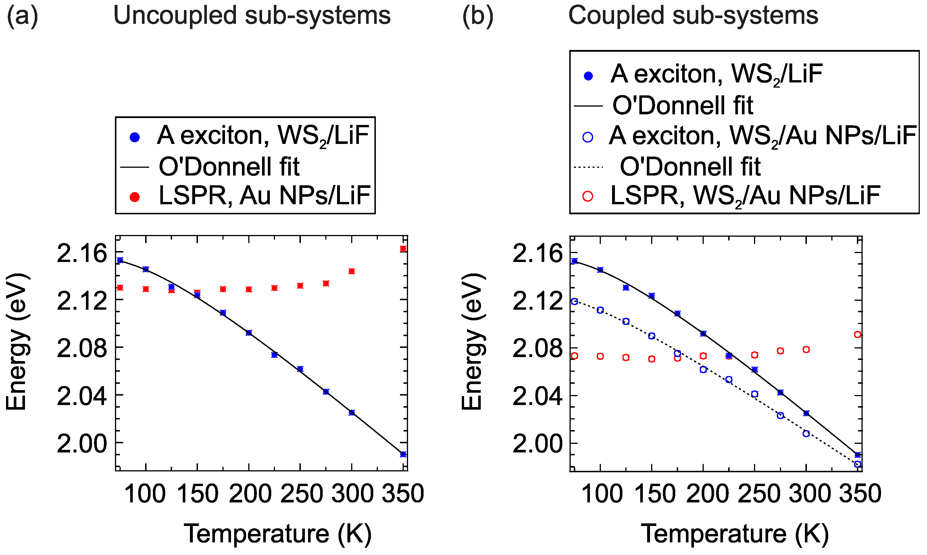
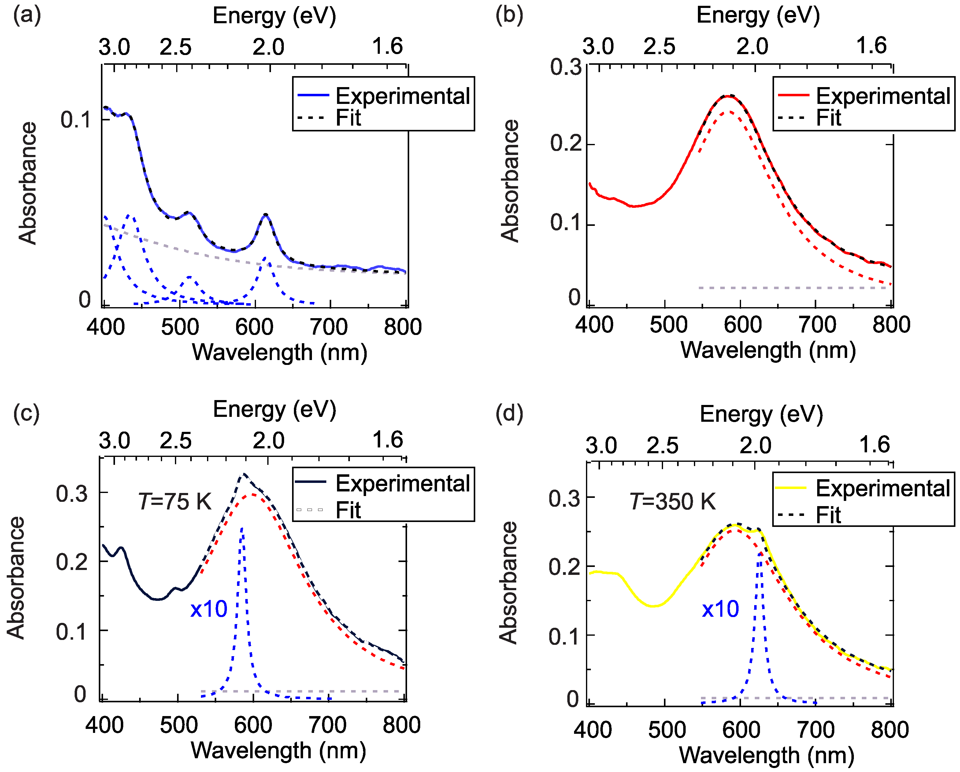
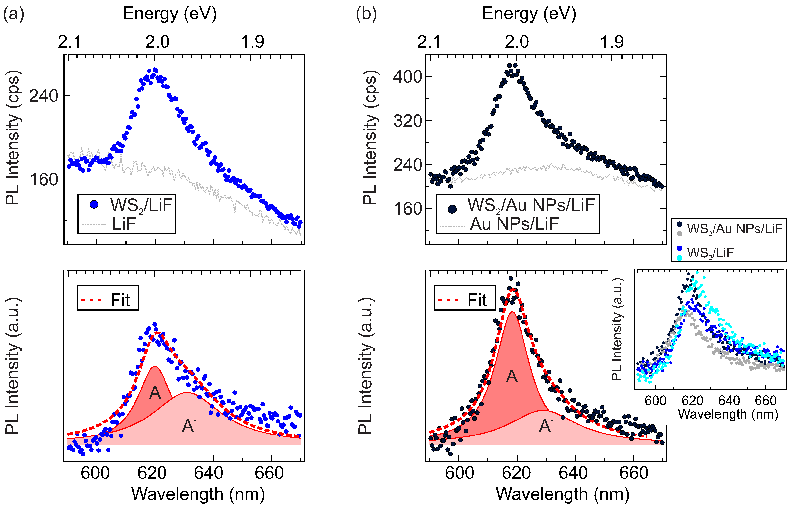
The microscopic PL characterization was performed in a Horiba Xplora Plus confocal Raman microscope, (HORIBA Jobin Yvon GmbH - Bensheim, Bensheim, Germany). A laser beam with a wavelength of 532 nm and a power of 100 μ W was focused with a 10× objective on the sample surface. The diameter of the laser spot at the surface was approximately 1 μ m. After light-sample interaction, the light was collected in a back-scattering geometry. The measurements were performed at room temperature with a spectral resolution of 0.5 nm.

3. Results

Figure 1a shows a representative optical image of the hybrid system acquired with 10× magnification in a region where the WS 2 flakes are in direct contact with the Au NPs. The ML-WS 2 flakes form a triangular shape with an edge-to-edge length of ∼200 μ m each. In Figure 1b, a 2 × 2 μ m 2 atomic force microscopy (AFM) image across the edge of the WS 2 flake is shown. Outside the flake, closely packed Au NPs appear, with an average spacing of 21 ± 2 nm along the uniaxial LiF direction (see Appendix A, Figure A1a,b for details on the plasmonic substrate).
In Figure 1c, we report representative absorbance spectra of the WS 2 /Au hybrid system, measured at room temperature. Micro-absorbance spectra of the two uncoupled sub-systems, namely WS 2 /LiF and Au NPs/LiF, are also shown. The blue curve corresponds to ML-WS 2 on bare LiF. The A, B and C excitonic peaks of WS 2 can be seen at 2.019 ± 0.001 eV, 2.415 ± 0.001 eV and 2.847 ± 0.003 eV, respectively, in agreement with the literature [54,55,56,57]. The dashed black line is a Lorentzian fit (see Appendix B, Figure A2a for details), and the solid grey line is the absorbance of the bare LiF substrate.
The red curve shows the absorption spectrum of the Au NP array, with the plasmonic peak at 2.125 ± 0.002 eV [48,58]. The dashed black curve is a Lorentzian fit (see Appendix B, Figure A2b for details). The solid black line is the absorbance of the ML-WS 2 /Au NP heterostructure. The black curve shows features belonging to both the plasmonic Au and WS 2 , as already observed for other hybrid systems [59]. A clear evidence of the interaction between the two sub-systems and, thus, of the fact that the spectrum is not simply the sum of the absorbances of the separated sub-systems, is the redshift of the LSPR peak, ascribed to the effective refractive index increase of the optical environment of the NPs [60,61]. A slight redshift of approximately 10 meV is observed also for the A-exciton feature in the hybrid medium, with respect to the reference WS 2 /LiF, as highlighted by the vertical dashed blue line in the graph.
In Figure 1d, we report two representative PL spectra acquired on ML-WS 2 on Au NPs (black markers) and on bare LiF (blue markers). The two data sets were normalized to the respective substrate signal and deconvolved as a superposition of different excitonic contributions (see Appendix C, Figure A3a,b). The black curve peaks at about 2.005 ± 0.002 eV, whereas the blue curve has its maximum around 2.000 ± 0.002 eV, as estimated from the fitting curves (dashed red lines).
The WS 2 /LiF system exhibits a Stokes shift approximately 20 meV larger than WS 2 /Au NPs, a fact that can be ascribed to electron doping of the flake and the occurrence of structural disorder [62,63], which are known to affect the local excitonic properties of CVD-grown TMDC flakes. Concerning the PL intensity, no remarkable variation is induced by the Au NPs.
To delve deeper into the properties of the hybrid medium, we investigated the absorbance as a function of the thickness t of the intercalated LiF layer, from 0 to 10 nm (see sketch in Figure 2a). The legend next to the sketch shows the spacer thicknesses for which we extracted the absorbance spectra reported in the graphs of panels (b) and (c). In detail, in Figure 2b, we report the absorbance spectra, as a function of t, of Au NPs alone. For increasing t, from black to yellow, we observe a gradual redshift of the LSPR, quantified in the inset of Figure 2b. In the inset, the dashed black curve is an exponential fit. The redshift between t = 0 and t = 10 nm is around 58 meV. The redshift can be understood as being due to the increase of the effective dielectric function of the environment [64].
In the hybrid system, the absorbance reported in Figure 2c decreases as a function of increasing t. We hypothesized that this effect is related to the nano-morphology of the capping layer, the thickness of which is ultimately comparable with the NP size and with the interparticle gaps. This is accompanied by a redshift of the LSPR peak with respect to Au NPs without WS 2 , that fades as t increases until stabilizing for t greater than ∼7 nm (orange curve), where the two sub-systems apparently cease interacting.
To better appreciate this trend, we overlapped in Figure 2d the absorbance spectra of the hybrid system when the dielectric spacer is absent (solid black curve) and in the presence of a 7 nm thick spacer (solid orange curve). In the first case, the LSPR of Au NPs in the hybrid system undergoes a spectral redshift with respect to the LSPR peak of Au NPs without WS 2 (dashed black line). In the presence of a 7 nm thick (or thicker) spacer, the absorbance of the hybrid system becomes the incoherent sum of the Au NPs (dashed orange) and ML-WS 2 (blue) spectra.
Having ascertained the conditions under which an interaction is present between the two subcomponents at RT, we investigated the temperature evolution of the optical response of WS 2 flakes in direct contact with Au NPs. In order to assess correctly the behaviour of the hybrid system, we began by addressing the temperature response of the two separated sub-systems in order to later exploit it as a reference.
Figure 3a shows the absorbance spectra of ML-WS 2 /LiF and of the Au NPs/LiF, from 75 (black) to 350 K (yellow) in the 1.55–3.10 eV energy range. In ML-WS 2 /LiF, the temperature increase induces a redshift, broadening and weakening of the exciton peaks. This is highlighted in Figure 3c, where some curves at selected T over the A exciton spectral range are shown. A redshift of about 163 meV is detected in the 75–350 K temperature range. Within the same temperature interval, the LSPR absorbance peak of the Au NP array shows a slight broadening and an intensity decrease of about 22% (see Figure 3d). The spectral position of the LSPR peak remains almost unaltered up to 275 K, at ∼2.13 eV, while it starts blueshifting from RT onward, by approximately 33 meV at 350 K with respect to 75 K.
For the WS 2 /Au NP heterostructure (see Figure 3b), the T-dependent optical response is characterized by a trend reminiscent of the superposition of the two uncoupled systems with some variations due to the interaction of the Au NPs with the WS 2 flake.
The overall absorbance of the hybrid system stays fairly constant up to RT. Then, it starts decreasing for higher temperatures. The LSPR-related component, extracted from the fitting of the hybrid system absorbance spectra (see Figure A2c,d) blueshifts by approximately 70 meV between LT and 350 K. The A-exciton feature is superimposed on the LSPR peak and redshifts with increasing T from 2.113 ± 0.002 eV to 1.989 ± 0.002 eV, crossing the LSPR peak, as displayed in Figure 3e.

4. Discussion

In Figure 4a, we plotted the temperature dependence of the A-exciton (blue markers) and the LSPR (red markers) energies in the 75–350 K T range for the two uncoupled sub-systems. The T dependence of the A-exciton energy ( E A ( T ) ) can be described in the framework of the O’Donnell model by using the following equation [65]
E A ( T ) = E A ( 0 ) s ħ ω coth ħ ω 2 k B T 1 ,
in which E A ( 0 ) is the A exciton energy at T = 0 K, s takes into account the exciton–phonon interaction, ħ ω corresponds to the average phonon energy, and k B is the Boltzmann constant. By fitting the blue curve in Figure 4a (solid black line), we obtained E A ( 0 ) = 2.157 ± 0.002 eV, s = 4.4 ± 0.2 eV and ħ ω = 26 ± 2 meV, in agreement with the values reported in literature for similar systems [61,66]. From the graph, we can notice that the LSPR energy matches the A-exciton energy of standalone WS 2 /LiF in the 125–175 K temperature range.
In Figure 4b, we compare the A-exciton energies in the standalone (filled blue circles) and coupled case (open blue circles). The exciton redshifts when in contact with the Au NPs, with respect to the LiF substrate, and the amount of this redshift decreases for increasing temperature. Fitting the E A ( T ) of the hybrid system (black dashed line), we obtained E A ( 0 ) = 2.125 ± 0.003 eV, s = 3.4 ± 0.2 eV and ħ ω = 21 ± 3 meV. The hybrid system shows a weaker dependence of the exciton energy on temperature compared to WS 2 /LiF, in line with previous observations [67], and a remarkable difference in the exciton energy extrapolated at 0 K [68].
In previous works [68], this was ascribed to the presence of strain within ML-WS 2 flakes caused by a thermal expansion coefficient mismatch between the TMDC layer and the substrate. In addition, TMDC flakes transferred on top of a nanostructured metallic substrate exhibit local heterogeneities in strain depending on the patterning of the plasmonic substrate underneath [60,69], thereby, justifying our observations [70].
From Figure 4b, we can notice that the energies of the LSPR and the exciton in the WS 2 /Au system cross each other between 175 and 200 K. The corresponding spectra do not, however, show any evidence of intermediate or strong-coupling regimes, like the avoided crossing or the transparency dip typical of Fano-type interference. Concerning this, see, for example, the purple curve marked by an arrow in Figure 3e acquired at 175 K, in which the A exciton and LSPR energies match. We note that different excitation conditions in the micro-transmittance measurements (e.g., out-of-plane polarized light) would not change the coupling regime, due to spectrally-shifted LSPR modes and the need for in-plane field components to achieve exciton formation.
The observed behaviour, i.e., the absence of intermediate or strong-coupling despite the extremely close proximity between the two sub-systems, can be rationalized considering the Au-NP geometry. This type of NP arrays is indeed characterized by NP densities as high as 10 3 NPs/ μ m 2 , and interparticle gaps below 10 nm [71]. Accordingly, the EM field is highly confined in the gaps between the Au NPs; whereas, on top of the NPs, where the WS 2 flake lies, the field intensities are usually rather weak. An example of calculating the distribution of the local electric field intensity on the NP surface for the plasmonic excitation is reported in Ref. [72]. This suggests that the mutual overlap of the EM near field that would justify the coupling of excitons in WS 2 with plasmons is relatively weak, explaining the experimental observations.

5. Conclusions

In this work, we investigated the optical response of the ML-WS 2 /Au NPs heterostructure by means of temperature-dependent optical microscopic spectroscopies. The hybrid system was composed of CVD-grown WS 2 flakes transferred on top of a densely-packed array of Au NPs. We studied the influence of a dielectric spacer with a thickness gradient inserted between the NPs and the WS 2 flakes on the optical properties of the system.
Temperature-dependent transmittance measurements with microscopic lateral resolution were performed to investigate the A exciton and LSPR energy trends in the 75–350 K temperature interval. The presence of a plasmon–exciton interaction in the weak-coupling regime can be ascribed to the morphology of the hybrid system and to the fact that the electromagnetic field is highly confined in the gap region between the Au NPs of the plasmonic array.
The presence of Au NPs affects the temperature-dependence of the optical bandgap of ML-WS 2 , which, compared to the ML-WS 2 /LiF system, shows a redshift. The observed trends confirm, once again, the pivotal role of the substrate in affecting the optical properties of TMDCs.
In general, 2D TMDCs placed on top of an ultra-dense plasmonic substrate can be an interesting system to be exploited, for example, for applications in the field of molecular sensing.

Author Contributions

Conceptualization, M.F. and F.B.; methodology and investigation, M.F., L.R., D.C., G.O., S.P., I.M., M.M., M.R. and F.B.; validation, M.F.; formal analysis, M.F. and F.B.; data curation, M.F.; writing–original draft preparation, review and editing, M.F. and F.B.; visualization, M.F.; supervision, project administration, and funding acquisition, F.B., M.C., C.C. and D.R.T.Z. All authors have read and agreed to the published version of the manuscript.

Funding

The research leading to these results has received funding from Compagnia di San Paolo (project STRATOS) and Ministero dell’Istruzione, dell’Università e della Ricerca: PRIN 2017 grant number 2017KFY7XF and Dipartimenti di Eccellenza 2018–2022. We acknowledge support from DAAD (German Academic Exchange Service) Research Grants—Short-Term Grants, 2021 (57552336). This research has also received funding from the European Union’s Horizon 2020 research and innovation program under grant agreement no. 881603-GrapheneCore3. This research was also funded by Deutsche Forschungsgemeinschaft (DFG) grant numbers ZA 146/43-1, ZA 146/44-1 and FL 670/8-1.

Institutional Review Board Statement

Not applicable.

Informed Consent Statement

Not applicable.

Data Availability Statement

The data presented in this study are available on request from the corresponding author.

Conflicts of Interest

The authors declare no conflict of interest.

Appendix A. Plasmonic Substrate

In Figure A1a, we report an AFM image to investigate the morphological properties of the plasmonic substrate. The plasmonic substrate is a densely-packed array of Au NPs with an areal density of approximately 827 ± 15 NPs/ μ m 2 and a mean NP volume of about 3627 ± 64 nm 3 , as extracted from the digital analysis [47] of the AFM image. In detail, the Au NP chains elongate along the [001] direction with a mean NP distance of 21 ± 2 nm.
The mean NP distance across the chains is about 25 ± 2 nm. From the absorbance spectra of the plasmonic array acquired by linearly polarizing the incident light beam along (blue) and across (red) the NP chains (see Figure A1b), it can be observed that the system anisotropy slightly influences the spectral position of the LSPR, which undergoes a tiny shift of approximately 6 nm by varying the polarization. In the manuscript, all the micro-transmittance measurements were acquired by using a light beam polarized along the NP chains.
Figure A1. (a) AFM image of the plasmonic array of Au NPs. The scanned area is 2 × 2 μ m 2 . The white arrow indicates the elongation direction of the Au NP chains. The red and blue arrows correspond to the light linear polarization direction, respectively, parallel and perpendicular to the Au NP chains. (b) In the graph, the corresponding absorbance spectra are shown.
Chemosensors 10 00120 g0a1

Appendix B. Deconvolution of Micro-Absorbance Spectra

Figure A2a shows the deconvolution of the micro-absorbance spectrum of ML-WS 2 /LiF acquired at RT. The fitting curve (black dashed line) is obtained by the superimposition of four Lorentzian peaks (dashed blue) on a cubic background (dashed grey curve). In detail, the Lorentzian peaks associated to the A, B and C excitons are located, respectively, at 2.019 ± 0.002 eV, 2.415 ± 0.002 eV and 2.847 ± 0.002 eV. The micro-absorbance spectrum of the Au NPs is fitted above 545 nm, where the interband transitions are not present, by using a single Lorentzian peak (dashed red curve) superimposed on a constant background (dashed grey line).
In the graphs of Figure A2c,d, we report an example of fitting of the hybrid system micro-absorbance spectra acquired, respectively, at 75 K (solid black curve, panel (c)) and 350 K (solid yellow curve, panel (d)). The fitting was performed in the spectral region, which comprises the maximum of the absorbance spectra, by using two Lorentzian peaks, one for the LSPR of Au NPs (dashed red peak) and the other for the A exciton of ML-WS 2 (dashed blue peak, multiplied by 10 in the graph). A constant background was used (dashed grey line).
Figure A2. Deconvolution of the micro-absorbance spectra of (a) ML-WS 2 /LiF (solid blue), (b) Au NPs/LiF (solid red), (c) ML-WS 2 /Au NPs/LiF at T = 75 K (solid black) and (d) ML-WS 2 /Au NPs/LiF at T = 350 K (solid yellow). In the graphs, the dashed grey lines correspond to the backgrounds, the dashed blue peaks to excitonic features (multiplied by 10 in panels (c,d)), the dashed red peak to the plasmonic resonance and the black dashed lines to the fitting curves (dashed white curve in the graph of panel (c)).
Chemosensors 10 00120 g0a2

Appendix C. Deconvolution of Micro-PL Spectra

In the top graphs of Figure A3a,b, we show the PL spectra, respectively, of ML-WS 2 /LiF (blue circles) and ML-WS 2 /Au NPs/LiF (black circles). To these curves, we overlapped the spectral response of the bare substrates (dotted grey curves), LiF (panel (a)) and Au NPs/LiF (panel (b)), respectively. The PL spectral deconvolution is shown in the bottom graph.
The fitting curves are reported as dashed red lines. In detail, two Lorentzian peaks, corresponding to neutral (A, dark red) and charged exciton (A , light red), contribute to the PL of ML-WS 2 . The energy shift between A and A peaks is about 34 meV, and the full-width at half maximum (fwhm) of A and A exciton peaks is approximately 47 and 90 meV. In addition, the A/A intensity ratio is higher for the WS 2 /LiF system. This may be caused by a n-type doping coming from the LiF substrate, which may also explain the higher Stokes shift observed for the WS 2 /LiF system with respect to the WS 2 /Au NPs/LiF system, as discussed in the main text.
In the inset graph, we show some other PL spectra extracted from different regions of the WS 2 flakes, respectively, on top of LiF (blue and light blue markers) and of Au NPs (black and grey circles). As observed in the main text, it seems that the Au NPs do not affect the PL intensity signal.
Figure A3. The top graphs show the PL spectra of (a) ML-WS 2 /LiF (blue circles) and (b) ML-WS 2 /Au NPs/LiF (black circles). The dotted grey curves correspond to the spectral response of the corresponding bare substrates, LiF and Au NPs/LiF, respectively. The bottom graphs report the deconvolution of the PL peak after having been normalized to the bare substrate. The PL spectrum is the sum of neutral (A, dark red) and charged (A , light red) exciton contributions. The fitting curves are reported in dashed red. The inset shows some other PL spectra acquired from different spots of the WS 2 flakes on LiF (blue and light blue circles) and on Au NPs (black and grey circles).
Chemosensors 10 00120 g0a3

References

  1. Wilson, J.A.; Yoffe, A.D. The transition metal dichalcogenides discussion and interpretation of the observed optical, electrical and structural properties. Adv. Phys. 1969, 18, 193–335. [Google Scholar] [CrossRef]
  2. Chhowalla, M.; Shin, H.S.; Eda, G.; Li, L.-J.; Loh, K.P.; Zhang, H. The chemistry of two-dimensional layered transition metal dichalcogenide nanosheets. Nat. Chem. 2013, 5, 263–275. [Google Scholar] [CrossRef]
  3. Butler, S.Z.; Hollen, S.M.; Cao, L.; Cui, Y.; Gupta, J.A.; Gutiérrez, H.R.; Heinz, T.F.; Hong, S.S.; Huang, J.; Ismach, A.F.; et al. Progress, challenges, and opportunities in two-dimensional materials beyond graphene. ACS Nano 2013, 7, 2898–2926. [Google Scholar] [CrossRef] [PubMed]
  4. Manzeli, S.; Ovchinnikov, D.; Pasquier, D.; Yazyev, O.V.; Kis, A. 2D transition metal dichalcogenides. Nat. Rev. Mater. 2017, 2, 71033. [Google Scholar] [CrossRef]
  5. Samadi, M.; Sarikhani, N.; Zirak, M.; Zhang, H.; Zhang, H.L.; Moshfegh, A. Group 6 transition metal dichalcogenide nanomaterials: Synthesis, applications and future perspectives. Nanoscale Horiz. 2018, 3, 90–204. [Google Scholar] [CrossRef]
  6. Splendiani, A.; Sun, L.; Zhang, Y.; Li, T.; Kim, J.; Chim, C.-Y.; Galli, G.; Wang, F. Emerging photoluminescence in monolayer MoS2. Nano Lett. 2010, 10, 1271–1275. [Google Scholar] [CrossRef] [PubMed]
  7. Mak, K.F.; Lee, C.; Hone, J.; Shan, J.; Heinz, T.F. Atomically-thin MoS2: A new direct-gap semiconductor. Phys. Rev. Lett. 2010, 105, 136805. [Google Scholar] [CrossRef] [PubMed] [Green Version]
  8. Liu, Y.; Weiss, N.O.; Duan, X.; Cheng, H.-C.; Huang, Y.; Duan, X. Van der Waals heterostructures and devices. Nat. Rev. Mater. 2016, 1, 16042. [Google Scholar] [CrossRef]
  9. Choi, W.; Choudhary, N.; Han, G.H.; Park, J.; Akinwande, D.; Lee, Y.H. Recent development of two-dimensional transition metal dichalcogenides and their applications. Mater. Today 2017, 20, 116–130. [Google Scholar] [CrossRef]
  10. Wang, Q.H.; Kalantar-Zadeh, K.; Kis, A.; Coleman, J.N.; Strano, M.S. Electronics and optoelectornics of two-dimensional transition metal dichalcogenides. Nat. Nanotech. 2012, 7, 699–712. [Google Scholar]
  11. Mak, K.F.; Shan, J. Photonics and optoelectronics of 2D semiconductor transition metal dichalcogenides. Nat. Photonics 2016, 10, 216–226. [Google Scholar] [CrossRef]
  12. Zeng, Q.; Liu, Z. Novel optoelectronic devices: Transition-metal-dichalcogenide-based 2D heterostructures. Adv. Electron. Mater. 2018, 4, 1700335. [Google Scholar] [CrossRef]
  13. Wang, G.; Chernikov, A.; Glazov, M.M.; Heinz, T.F.; Marie, X.; Amand, T.; Urbaszek, B. Colloquium: Excitons in atomically thin transition metal dichalcogenides. Rev. Mod. Phys. 2018, 90, 021001. [Google Scholar] [CrossRef] [Green Version]
  14. Cheiwchanchamnangij, T.; Lambrecht, W.R.L. Quasiparticle band structure calculation of monolayer, bilayer, and bulk MoS2. Phys. Rev. B 2012, 85, 205302. [Google Scholar] [CrossRef] [Green Version]
  15. Ramasubramaniam, A. Large excitonic effects in monolayers of molybdenum and tungsten dichalcogenides. Phys. Rev. B 2012, 115, 115409. [Google Scholar] [CrossRef] [Green Version]
  16. Qiu, D.Y.; da Jornada, F.H.; Louie, S.G. Optical spectrum of MoS2: Many-body effects and diversity of exciton states. Phys. Rev. Lett. 2013, 111, 216805. [Google Scholar] [CrossRef] [Green Version]
  17. Chernikov, A.; Berkelbach, T.C.; Hill, H.M.; Rigosi, A.; Li, Y.; Aslan, O.B.; Reichman, D.R.; Hybertsen, M.S.; Heinz, T.F. Exciton binding energy and nonhydrogenic Rydberg series in monolayer WS2. Phys. Rev. Lett. 2014, 113, 076802. [Google Scholar] [CrossRef] [Green Version]
  18. He, K.; Kumar, N.; Zhao, L.; Wang, Z.; Mak, K.F.; Zhao, H.; Shan, J. Tightly bound excitons in monolayer WSe2. Phys. Rev. Lett. 2014, 113, 026803. [Google Scholar] [CrossRef] [Green Version]
  19. Yu, H.; Cui, X.; Xu, X.; Yao, W. Valley excitons in two-dimensional semiconductors. Natl. Sci. Rev. 2015, 2, 57–70. [Google Scholar] [CrossRef]
  20. Mueller, T.; Malic, E. Exciton physics and device application of two-dimensional transition metal dichalcogenides semiconductors. npj 2D Mater. Appl. 2018, 2, 29. [Google Scholar] [CrossRef] [Green Version]
  21. Yan, S.; Zhu, X.; Dong, J.; Ding, Y.; Xiao, S. 2D materials integrated with metallic nanostructures: Fundamentals and optoelectronic applications. Nanophotonics 2020, 9, 1877–1900. [Google Scholar] [CrossRef]
  22. Sriram, P.; Manikandan, A.; Chuang, F.-C.; Chueh, Y.-L. Hybridizing plasmonic materials with 2D-transition metal dichalcogenides toward functional applications. Small 2020, 16, 1904271. [Google Scholar] [CrossRef] [PubMed]
  23. Tao, L.; Chen, Z.; Li, Z.; Wang, J.; Xu, X.; Xu, J.-B. Enhancing light-matter interaction in 2D materials by optical micro/nano architectures for high-performance optoelectronic devices. InfoMat 2021, 3, 36–60. [Google Scholar] [CrossRef]
  24. Maier, S.A. Localized surface plasmons. In Plasmonics: Fundamentals and Applications; Springer: New York, NY, USA, 2007; pp. 65–88. [Google Scholar]
  25. Pluchery, O. Optical properties of gold nanoparticles. In Gold Nanoparticles for Physics, Chemistry and Biology; Louis, C., Pluchery, O., Eds.; Imperial College Press: London, UK, 2012; pp. 43–73. [Google Scholar]
  26. Yang, Y.; Liu, W.G.; Lin, Z.T.; Pan, R.H.; Gu, C.Z.; Li, J.J. Plasmonic hybrids of two-dimensional transition metal dichalcogenides and nanoscale metals: Architectures, enhanced optical properties and devices. Mater. Today Phys. 2021, 17, 100343. [Google Scholar] [CrossRef]
  27. Giannini, V.; Fernández-Domínguez, A.I.; Heck, S.C.; Maier, S.A. Plasmonic nanoantennas: Fundamentals and their use in controlling the radiative properties of nanoemitters. Chem. Rev. 2011, 111, 3888–3912. [Google Scholar] [CrossRef] [PubMed]
  28. Eda, G.; Maier, S.A. Two-dimensional crystals: Managing light for optoelectronics. ACS Nano 2013, 7, 5660–5665. [Google Scholar] [CrossRef]
  29. Jiang, R.; Li, B.; Fang, C.; Wang, J. Metal/semiconductor hybrid nanostructures for plasmon-enhanced applications. Adv. Mater. 2014, 26, 5274–5309. [Google Scholar] [CrossRef]
  30. Li, X.; Zhu, J.; Wei, B. Hybrid nanostructures of metal/two-dimensional nanomaterials for plasmon-enhanced applications. Chem. Soc. Rev. 2016, 45, 3145–3187. [Google Scholar] [CrossRef] [Green Version]
  31. Wang, Z.; Dong, Z.; Gu, Y.; Chang, Y.-H.; Zhang, L.; Li, L.-J.; Zhao, W.; Eda, G.; Zhang, W.; Grinblat, G.; et al. Giant photoluminescence enhancement in tungsten-diselenide gold plasmonic hybrid structures. Nat. Commun. 2016, 7, 11283. [Google Scholar] [CrossRef] [Green Version]
  32. Palacios, E.; Park, S.; Lauhon, L.; Aydin, K. Identifying excitation and emission rate contributions to plasmon-enhanced photoluminescence for monolayer MoS2 using a tapered gold nanoantenna. ACS Photonics 2017, 4, 1602–1606. [Google Scholar] [CrossRef]
  33. Li, Z.; Liu, C.; Rong, X.; Luo, Y.; Cheng, H.; Zheng, L.; Lin, F.; Shen, B.; Gong, Y.; Zhang, S.; et al. Tailoring MoS2 valley-polarized photoluminescence with super chiral near-field. Adv. Mater. 2018, 30, 1801908. [Google Scholar] [CrossRef]
  34. Shi, J.; Liang, W.-Y.; Raja, S.S.; Sang, Y.; Zhang, X.-Q.; Chen, C.-A.; Wang, Y.; Yang, X.; Lee, Y.-H.; Ahn, H.; et al. Plasmonic enhancement and manipulation of optical nonlinearity in monolayer tungsten disulfide. Laser Photonics Rev. 2018, 12, 1800188. [Google Scholar] [CrossRef]
  35. Wang, Z.; Dong, Z.; Zhu, H.; Jin, L.; Chiu, M.-H.; Li, L.-J.; Xu, Q.-H.; Eda, G.; Maier, S.A.; Wee, A.T.S.; et al. Selectively plasmon-enhanced second-harmonic generation from monolayer tungsten diselenide on flexible substrates. ACS Nano 2018, 12, 1859–1867. [Google Scholar] [CrossRef] [PubMed] [Green Version]
  36. Li, Z.; Xiao, Y.; Gong, Y.; Wang, Z.; Kang, Y.; Zu, S.; Ajayan, P.M.; Nordlander, P.; Fang, Z. Active light control of the MoS2 monolayer exciton binding energy. ACS Nano 2015, 9, 10158–10164. [Google Scholar]
  37. Chen, Y.-H.; Tamming, R.R.; Chen, K.; Zhang, Z.; Hodgkiss, J.M.; Blaikie, R.J.; Ding, B.; Qiu, M. Bandgap control in two-dimensional semiconductors via coherent doping of plasmonic hot electrons. Nat. Commun. 2021, 12, 4332. [Google Scholar] [CrossRef]
  38. Kang, Y.; Najmaei, S.; Liu, Z.; Bao, Y.; Wang, Y.; Zhu, X.; Halas, N.J.; Nordlander, P.; Ajayan, P.M.; Lou, J.; et al. Plasmonic hot electron induced structural phase transition in MoS2 monolayer. Adv. Mater. 2014, 26, 6467–6471. [Google Scholar] [CrossRef] [PubMed]
  39. Milekhin, A.G.; Rahaman, M.; Rodyakina, E.E.; Latyshev, A.V.; Dzhagan, V.M.; Zahn, D.R.T. Giant gap-plasmon tip-enhanced Raman scattering of MoS2 monolayers of Au nanocluster arrays. Nanoscale 2018, 10, 2755–2763. [Google Scholar] [CrossRef] [PubMed]
  40. Gonçalves, P.A.D.; Stenger, N.; Cox, J.D.; Mortensen, N.A.; Xiao, S. Strong light-matter interactions enabled by polaritons in atomically thin materials. Adv. Opt. Mater. 2020, 8, 1901473. [Google Scholar] [CrossRef]
  41. Yankovich, A.B.; Munkhbat, B.; Baranov, D.G.; Cuadra, J.; Olsén, E.; Lourenço-Martins, H.; Tizei, L.H.G.; Kociak, M.; Olsson, E.; Shegai, T. Visualizing spatial variations of plasmon–exciton polaritons at the nanoscale using electron microscopy. Nano Lett. 2019, 19, 8171–8181. [Google Scholar] [CrossRef] [PubMed] [Green Version]
  42. Liu, L.; Tobing, L.Y.M.; Tong, J.; Qiang, B.; Fernández-Domínguez, A.I.; Garcia-Vidal, F.J.; Zhang, D.H.; Wang, Q.J.; Luo, Y. Strong plasmon–exciton interactions on nanoantenna array-monolayer WS2 hybrid system. Adv. Opt. Mater. 2020, 8, 1901002. [Google Scholar]
  43. Proietti Zaccaria, R.; Bisio, F.; Das, G.; Maidecchi, G.; Caminale, M.; Duc Vu, C.; De Angelis, F.; Di Fabrizio, E.; Toma, A.; Canepa, M. Plasmonic color-graded nanosystems with achromatic subwavelength architectures for light filtering and advanced SERS detection. ACS Appl. Mater. Interfaces 2016, 8, 8024–8031. [Google Scholar] [CrossRef] [PubMed] [Green Version]
  44. Kasani, S.; Curtin, K.; Wu, N. A review of 2D and 3D plasmonic nanostructure array patterns: Fabrication, light management and sensing applications. Nanophotonics 2019, 8, 2065–2089. [Google Scholar] [CrossRef]
  45. Chen, P.X.; Qiu, H.W.; Xu, S.C.; Liu, X.Y.; Li, Z.; Hu, L.T.; Li, C.H.; Guo, J.; Jiang, S.Z.; Huo, Y.Y. A novel surface-enhanced Raman spectroscopy substrate based on a large area of MoS2 and Ag nanoparticles hybrid system. Appl. Surf. Sci. 2016, 375, 207–214. [Google Scholar] [CrossRef]
  46. Alamri, M.; Sakidja, R.; Goul, R.; Ghopry, S.; Wu, J.Z. Plasmonic Au Nanoparticles on 2D MoS2/Graphene van der Waals heterostructures for high-sensitivity surface-enhanced Raman spectroscopy. ACS Appl. Nano Mater. 2019, 2, 1412–1420. [Google Scholar] [CrossRef]
  47. Magnozzi, M.; Ferrera, M.; Mattera, L.; Canepa, M.; Bisio, F. Plasmonics of Au nanoparticles in a hot thermodynamic bath. Nanoscale 2019, 11, 1140–1146. [Google Scholar] [CrossRef]
  48. Ferrera, M.; Magnozzi, M.; Canepa, M.; Bisio, F. Thermoplasmonics of Ag nanoparticles in a variable-temperature bath. J. Phys. Chem. C 2020, 124, 17204–17210. [Google Scholar] [CrossRef]
  49. Conti, S.; Pimpolari, L.; Calabrese, G.; Worsley, R.; Majee, S.; Polyushkin, D.K.; Paur, M.; Pace, S.; Keum, D.H.; Fabbri, F.; et al. Low voltage 2D materials-based printed field-effect transistors for integrated digital and analog electronics on paper. Nat. Commun. 2020, 11, 3566. [Google Scholar] [CrossRef]
  50. Pace, S.; Martini, L.; Convertino, D.; Keum, D.H.; Forti, S.; Pezzini, S.; Fabbri, F.; Mišekis, V.; Coletti, C. Synthesis of large-scale monolayer 1T’-MoTe2 and its stabilization via scalable hBN encapsulation. ACS Nano 2021, 15, 4213–4225. [Google Scholar] [CrossRef]
  51. Magnozzi, M.; Pflug, T.; Ferrera, M.; Pace, S.; Ramó, L.; Olbrich, M.; Canepa, P.; Ağircan, H.; Horn, A.; Forti, S.; et al. Local optical properties of CVD-grown monolayer WS2 flakes. J. Phys. Chem. C 2021, 125, 16059–16065. [Google Scholar] [CrossRef]
  52. Mišekis, V.; Bianco, F.; David, J.; Gemmi, M.; Pellegrini, V.; Romagnoli, M.; Coletti, C. Deterministic patterned growth of high-mobility large-crystal graphene: A path towards wafer scale integration. 2D Mater. 2017, 4, 021004. [Google Scholar] [CrossRef]
  53. Coletti, C.; Giambra, M.A.; Miseikis, V.; Romagnoli, M. Graphene and Two-dimensional Materials Transfer Method by Using Free-Standing Bilayer Polymeric Membrane. WO/2020/201876, 19 March 2020. [Google Scholar]
  54. Li, Y.; Chernikov, A.; Zhang, X.; Rigosi, A.; Hill, H.M.; van der Zande, A.M.; Chenet, D.A.; Shih, E.-M.; Hone, J.; Heinz, T.F. Measurement of the optical dielectric function of monolayer transition-metal dichalcogenides: MoS2, MoSe2, WS2, and WSe2. Phys. Rev. B 2014, 90, 205422. [Google Scholar] [CrossRef] [Green Version]
  55. Liu, H.-L.; Shen, C.-C.; Su, S.-H.; Hsu, C.-L.; Li, M.-Y.; Li, L.-J. Optical properties of monolayer transition metal dichalcogenides probed by spectroscopic ellipsometry. Appl. Phys. Lett. 2014, 105, 201905. [Google Scholar] [CrossRef] [Green Version]
  56. Kozawa, D.; Kumar, R.; Carvalho, A.; Kumar Amara, K.; Zhao, W.; Wang, S.; Toh, M.; Ribeiro, R.M.; Castro Neto, A.H.; Matsuda, K.; et al. Photocarrier relaxation pathway in two-dimensional semiconducting transition metal dichalcogenides. Nat. Commun. 2014, 5, 4543. [Google Scholar] [CrossRef] [PubMed]
  57. Magnozzi, M.; Ferrera, M.; Piccinini, G.; Pace, S.; Forti, S.; Fabbri, F.; Coletti, C.; Bisio, F.; Canepa, M. Optical dielectric function of two dimensional WS2 on epitaxial graphene. 2D Mater. 2020, 7, 025024. [Google Scholar] [CrossRef]
  58. Ferrera, M.; Della Valle, G.; Sygletou, M.; Magnozzi, M.; Catone, D.; O’Keeffe, P.; Paladini, A.; Toschi, F.; Mattera, L.; Canepa, M.; et al. Thermometric calibration of the ultrafast relaxation dynamics of plasmonic Au nanoparticles. ACS Photonics 2020, 7, 959–966. [Google Scholar] [CrossRef]
  59. Butun, S.; Palacios, E.; Cain, J.D.; Liu, Z.; Dravid, V.P.; Aydin, K. Quantifying plasmon-enhanced light absorption in monolayer WS2 films. ACS Appl. Mater. Interfaces 2017, 9, 15044–15051. [Google Scholar] [CrossRef]
  60. Abid, I.; Bohloul, A.; Najamaei, S.; Avendano, C.; Liu, H.-L.; Péchou, R.; Mlayah, A.; Lou, J. Resonant surface plasmon–exciton interaction in hybrid MoSe2@Au nanostructures. Nanoscale 2016, 8, 8151–8159. [Google Scholar] [CrossRef]
  61. Abid, I.; Chen, W.; Yuan, J.; Bohloul, A.; Najmaei, S.; Avendano, C.; Péchou, R.; Mlayah, A.; Lou, J. Temperature-dependent plasmon–exciton interactions in hybrid Au/MoSe2 nanostructures. ACS Photonics 2017, 4, 1653–1660. [Google Scholar] [CrossRef]
  62. Yang, F.; Wilkinson, M.; Austin, E.J.; O’Donnell, K.P. Origin of the Stokes shift: A geometrical model of exciton spectra in 2D semiconductors. Phys. Rev. Lett. 1993, 70, 323–326. [Google Scholar] [CrossRef]
  63. Kolesnichenko, P.V.; Zhang, Q.; Yun, T.; Zheng, C.; Fuhrer, M.S.; Davis, J.A. Disentangling the effects of doping, strain and disorder in monolayer WS2 by optical spectroscopy. 2D Mater. 2020, 7, 025008. [Google Scholar] [CrossRef] [Green Version]
  64. Lance Kelly, K.; Coronado, E.; Zhao, L.L.; Schatz, G.C. The optical properties of metal nanoparticles: The influence of size, shape, and dielectric environment. J. Phys. Chem. B 2002, 107, 668–677. [Google Scholar] [CrossRef]
  65. O’Donnell, K.P.; Chen, X. Temperature dependence of semiconductor band gaps. Appl. Phys. Lett. 1991, 58, 2924. [Google Scholar] [CrossRef] [Green Version]
  66. Molas, M.R.; Nogajewski, K.; Slobodeniuk, A.O.; Binder, J.; Bartosa, M.; Potemski, M. The optical response of monolayer, few-layer and bulk tungsten disulfide. Nanoscale 2017, 9, 13128–13141. [Google Scholar] [CrossRef] [PubMed] [Green Version]
  67. Lo, T.W.; Zhang, Q.; Qiu, M.; Guo, X.; Meng, Y.; Zhu, Y.; Xiao, J.J.; Jin, W.; Leung, C.W.; Lei, D. Thermal redistribution of exciton population in monolayer transition metal dichalcogenides probed with plasmon–exciton coupling spectroscopy. ACS Photonics 2019, 6, 411–421. [Google Scholar] [CrossRef]
  68. Su, L.; Yu, Y.; Cao, L.; Zhang, Y. Effects of substrate type and material-substrate bonding on high-temperature behavior of monolayer WS2. Nano Res. 2015, 8, 2686–2697. [Google Scholar] [CrossRef]
  69. Rahaman, M.; Rodriguez, R.D.; Plechinger, G.; Moras, S.; Schüller, C.; Korn, T.; Zahn, D.R.T. Highly localized strain in MoS2/Au heterostructure revealed by tip-enhanced Raman spectroscopy. Nano Lett. 2017, 17, 6027–6033. [Google Scholar] [CrossRef]
  70. Conley, H.J.; Wang, B.; Ziegler, J.I.; Haglund, R.F., Jr.; Pantelides, S.T.; Bolotin, K.I. Bandgap engineering of strained monolayer and bilayer MoS2. Nano Lett. 2013, 13, 3626–3630. [Google Scholar] [CrossRef] [Green Version]
  71. Anghinolfi, L. Self-Organized Arrays of Gold Nanoparticles. Morphology and Plasmonic Properties; Springer: Berlin/Heidelberg, Germany, 2012. [Google Scholar]
  72. Magnozzi, M.; Proietti Zaccaria, R.; Catone, D.; O’Keeffe, P.; Paladini, A.; Toschi, F.; Alabastri, A.; Canepa, M.; Bisio, F. Interband transitions are more efficient than plasmonic excitation in the ultrafast melting of electromagnetically coupled Au nanoparticles. J. Phys. Chem. C 2019, 123, 16943–16950. [Google Scholar] [CrossRef]
Figure 1. (a) Optical image of CVD-grown ML-WS 2 flake on top of Au NPs on LiF substrate. No LiF spacer is present in this region. The image was taken with a 10× objective. (b) AFM image of the edge region between Au NPs and ML-WS 2 /Au NPs. The scanned area is 2 × 2 μ m 2 . (c) Micro-absorbance spectra of LiF substrate (grey), ML-WS 2 /LiF (blue), Au NPs/LiF (red) and of the hybrid system ML-WS 2 /Au NPs/LiF (solid black). The black dashed lines are the fitting curves of the absorbance spectra of WS 2 /LiF and Au NPs/LiF. The resonance features in ML-WS 2 correspond to A, B and C excitons. The vertical dashed blue line indicates the A exciton spectral position of ML-WS 2 . (d) Micro-PL spectra of ML-WS 2 /Au NPs/LiF (black circles) and ML-WS 2 /LiF (blue circles). The dashed red lines correspond to the fitting curves.
Chemosensors 10 00120 g001
Figure 2. (a) Sketch of the sample. The plasmonic substrate is composed of Au NP chains elongated along the grooves of the LiF substrate. A LiF dielectric layer with a thickness (t) gradient (from zero (black) up to 10 nm (yellow)) is interposed between the Au NPs and the WS 2 flakes, which are spread on the plasmonic substrate. For the graphs of panels (bd) the same color code reported in the legend (from black to yellow in the 0-10 nm t range) is shown. (b) Micro-absorbance spectra of Au NPs/LiF as a function of t. In the smaller graph the energy position of the Au LSPR as a function of t reported and fitted by means of an exponential function (black dashed curve). (c) Micro-absorbance spectra of the ML-WS 2 /Au NPs heterostructure as a function of t. (d) Comparison between the absorbance of the hybrid system in absence of the LiF spacer (solid black) and in the presence of a 7 nm thick spacer (solid orange). The dashed curves are the corresponding absorbance spectra of the Au NPs/LiF. The solid blue line is the spectrum of WS 2 /LiF, with the energy position of the A exciton marked by the vertical blue line.
Chemosensors 10 00120 g002
Figure 3. (a) Micro-absorbance spectra in the temperature range 75–350 K (from black to yellow) of the two sub-systems, Au NPs/LiF and WS 2 /LiF. (b) Micro-absorbance spectra in the temperature range 75–350 K (from black to yellow) of the WS 2 /Au NPs/LiF heterostructure. Zoom in the spectral region of (c) A exciton of ML-WS 2 /LiF, (d) the maximum of the LSPR peak of Au NPs/LiF and (e) the maximum in the absorbance spectra of the hybrid system, WS 2 /Au NPs/LiF.
Chemosensors 10 00120 g003
Figure 4. (a) Trend as a function of temperature of the energy position of the A exciton in ML-WS 2 /LiF (filled blue circles) and of LSPR in Au NPs/LiF (filled red circles). The continuous black line is fit to the A exciton energy by using the O’Donnell model [65]. (b) Trend as a function of temperature of the energy position of the A exciton (open blue circles) and of the LSPR of Au NPs (open red circles) in the WS 2 /Au NPs/LiF heterostructure. The A exciton energy of the ML-WS 2 /LiF sub-system (filled blue circles) is reported for comparison. Both solid and dashed black lines are fitting curves of the A exciton energy by using the O’Donnell model.
Chemosensors 10 00120 g004
Publisher’s Note: MDPI stays neutral with regard to jurisdictional claims in published maps and institutional affiliations.

