Article

Fabrication of Zinc Oxide Nanoparticles Deposited on (3-Aminopropyl) Triethoxysilane-Treated Silicon Substrates by an Optimized Voltage-Controlled Electrophoretic Deposition and Their Application as Fluorescence-Based Sensors

by
Fawwaz Hazzazi
1,
Alex Young
1,
Christopher O’Loughlin
1 and
Theda Daniels-Race
1,2,*
1
Division of Electrical and Computer Engineering, Louisiana State University, Baton Rouge, LA 70803, USA
2
Center for Computation & Technology, Louisiana State University, Baton Rouge, LA 70803, USA
*
Author to whom correspondence should be addressed.
Submission received: 1 October 2020 / Revised: 19 December 2020 / Accepted: 21 December 2020 / Published: 29 December 2020
(This article belongs to the Section Materials for Chemical Sensing)

Abstract

:
In this study, a voltage controlled, reproducible, scalable, and cost-effective approach for depositing zinc oxide (ZnO) nanoparticles (NPs), using electrophoretic deposition (EPD) onto p-type silicon (Si) substrates, has been researched and analyzed for its feasibility with respect to electronic device fabrication and fluorescence-based sensors. Our work presents a detailed investigation to evaluate the influence of ZnO morphology, ZnO concentration, and the method of surface treatment applied to the underlying Si substrates, because these pertain to an optimized EPD system. It has been noted that the ZnO NP structures formed directly atop the (3-aminopropyl) triethoxysilane (APTES)-treated Si substrates were more adhesive, thus resulting in a higher yield of NPs over that of comparable depositions on bare silicon. Our observation is that smaller particle sizes of ZnO will increase the energy emission for fluorescence transmission, eliminate several peak emissions, obtain higher fluorescence quantum yield (FQY) efficiency, and require less excitation energy. The results obtained are promising in relation to the integration of EPD in the fabrication of nano biosensors, PV solar cells, nano electronic devices, and thin film transistors (TFTs), where ZnO improves the reliability, affordability, and increased sensitivity needed for the next generation of nanoscale devices and systems.

1. Introduction

Nanoparticles and nanostructures are of great interest to the advancement of science and next generation technology due to their versatility in nano applications and highly sensitive surfaces [1,2,3,4,5]. Wurtzite zinc oxide (ZnO) nanostructures are n-type, II–VI semiconductor films that are of particular interest owing to their direct wide bandgap in the range of (3.3–3.37 eV), with high exciton binding energy around (60 meV) [6], which is higher than GaN, amendable optical properties [7], thermal and chemical stability, excellent biocompatibility and biosensing properties [8], and oxygen storage. Such a high quantity of exciton binding energy would suggest that ZnO has a stable and efficient excitonic emission, even beyond room temperature (RT) [9]. Delivering high transmittance in the visible range can be achieved by high direct bandgap [10,11]. Traits such as a wide direct optical band gap semiconductor and large exciton binding energy (60 meV) make ZnO a good material candidate for optoelectronic and optical biosensor devices applications [12,13,14]. Moreover, ZnO nanoparticles are easily reducible from zinc nitride and zinc acetate for applications such as nanostructure surfaces and gas sensing [15,16,17,18,19]. Physical properties of ZnO nanoparticles can be used in sensing, ultraviolent ranges, and thin film transistor (TFT) applications. Thus, physical properties of ZnO nanostructures are exploited in various applications including optoelectronics [20], filed emitters [21], UV lasers [22], solar cells [23], sensors [24,25,26,27,28,29], biosensors [12,30,31,32], and thin film transistor (TFT) [33,34,35,36].
Deposition of ZnO nanoparticles has already been performed by physical and chemical techniques. For instance, radio frequency magnetron sputtering systems [37], pulsed laser deposition [38], plasma enriched chemical vapor deposition (PE-CVD) [39], metal-organic chemical vapor deposition (MOCVD) [40], sol–gel system [41], molecular beam epitaxy [42], and atomic layer deposition [43] have been researched for their compatibility with nanomaterials and film quality for device and sensor applications. Lately, the electrophoretic deposition method has gained increasing attention both in academia and industrial sectors because of the wide versatility of its applications with different materials and because of its cost-effectiveness requiring simple apparatus [44]. Additionally, the controllability of the surface quality accomplished by varying the deposition parameters of the electrophoretic deposition (EPD) system to optimize morphology, surface structures, and optical performance [22,23]. In our previous studies, we have shown successful and controllable deposition of thin carbon nanotubes films using electrospray and electrophoretic deposition systems at room temperature (RT) without postdeposition or predisposition annealing [45,46].
In this paper, we show the study on ZnO nanoparticles (NPs) deposited by an electrophoretic deposition system at room temperature without post or pre-deposition annealing at high temperatures. The suitability of the two different surface functionalization and the ZnO deposition yield was studied. Furthermore, the influence of the concentration levels of ZnO in the EPD host solutions were divided into 5 and 10 wt% and its dependance of the structural and optical features were researched. The novelty in our approach is that we functionalized the experimental substrates by pre-deposition surface treatment, which was (3-aminopropyl) triethoxysilane (APTES); then, we optimized the EPD colloidal suspension for minimum surface defects and better electrophoretic deposited ZnO NP structures on p-silicon substrates. We believe that this, and other steps taken in this study, differentiates our work from that of other groups using EPD. The application of the studied surface as smoothness, crystallinity, and transparent conductive electrodes was exhibited and examined.

2. Materials and Methods

We dedicate this section to show steps, materials and procedures that were taken during the pre-deposition stage. The Chemical and Material Section addresses the materials and from where they were obtained. In Section 2.2, we mainly explain our design of the EPD system and what concentrations of ZnO NPs in the EPD solutions were used in our experiment for deposition. Electrodes play an important role in the EPD processes, thus Section 2.3 shows cleaning and treatment procedures of the silicon substrates and platinum electrodes. In Section 2.4, we describe the APTES treatment processes performed on several substrates. Then, we show our microfabrication overview of the EPD system for depositing a ZnO NP layer on p-Si and p-Si/APTES substrates. In the Synthesizing EPD ZnO Solution Section, we demonstrate the EPD host solution’s synthesizing and weight distribution. Finally, we specify the characterization instruments and studying aspects that we are researching.

2.1. Chemical and Material

The chemicals used for the electrodeposition of the ZnO structures were zinc oxide nanopowder (<50 nm particles, catalog number 677,450) and Poly(ethylene glycol) (H(OCH2CH2)nOH, catalog number 202,398), which were purchased from Sigma-Aldrich (Dongguan, China). The substrates used for electrophoretic deposition were p-type doped silicon wafers (boron dopant; resistivity = 10−20 ohm-cm; <100> orientation) from Shin-Etsu Handotai (SEH) (Tokyo, Japan). The electrodes for the EPD setup consisted of a 2 × 1 cm2 platinum (Pt) anode and a 2 × 1 cm2 p-type silicon cathode. Ethanol (C2H5OH) was used for preparation of the EPD ZnO NP solution. For cleaning purposes, we used nitric acid (HNO3), hydrochloric acid (HCl), and acetone, which were obtained from Fisher Scientific Lab Supplies (Fair Lawn, NJ, USA).

2.2. EPD Deposition Setup

Undoped 1 wt%, 5 wt%, and 10 wt% ZnO nanoparticle solutions were deposited by the electrophoretic method using the vertical set-up presented in Figure 1. The frame (6) was a 3D-printed glass-filled polyamide with dimensions of 50 × 50 × 50 cm3 and the substrate (3) was a platinum (Pt) plate heated at 200 °C by the thermo-controlled heater (6). The platinum to silicon samples distance was 2 cm and a voltage of 30 V was applied via a DC power supply (Applied Kilovolts, Sussex, UK). The EPD solvent was placed in a 20 mL beaker (2) positioned in the middle of the EPD setup (Figure 1). The Pt electrode (3) and Si substrates (4) were placed into the EPD solution (2) and connected to a DC voltage source (1).

2.3. Electrodes Preparation

Prior to the deposition of ZnO NP onto the electrodes via EPD, we cleaned the substrates thoroughly by sonication in an acetone bath for 2 h followed by cleaning with HCl and isopropyl alcohol (IPA) sequentially. Next, substrates were treated in a heated piranha suspension (H2SO4:H2O2) for 1 h to ensure removal of any organic material, followed by soaking and a wash in deionized (DI) water for 1 min. Finally, the substrates were dried by nitrogen gas. It is worth mentioning that the previous procedure of substrate cleaning was conducted only for silicon samples. However, for electrodes, platinum (Pt) and steel, we soaked these items for 10 min in warm HNO3 to remove impurities, followed by 10 min in warm KOH and a soak in DI water for 20 min (Figure 2c). The electrophoretic deposition of ZnO NPs was carried out in a two-electrode deposition setup, where the metal electrode serve as the anode and the target substrates serve as the cathode.

2.4. 3-Aminopropyl-Triethoxysilane (APTES) Surface Functionalization Treatment of ZnO Substrates

It has been shown in the literature that 3-aminopropyl-triethoxysilane (APTES) surface functionalization can be used to increase surface adhesion, improve film quality, and immobilize material on substrates for biomaterial sensors [25,26]. In our work, we immersed p-type silicon samples in a heated solution of APTES and ethanol (volume ratio 1:5) for 45 min. Thereafter, we dried these samples in a standard electronics laboratory oven for 50 min. Figure 2c shows the Si substrate surfaces after APTES treatment. From Figure 2d, it is clear that a new layer of APTES is on the substrate. Figure 2c, captured after the piranha cleaning, introduced a soft and clean layer of hydroxyl groups onto the p-type Si substrates by hydroxylation procedure. Afterwards, we continued the salinization procedure with the hydrolysis of ethoxy (–C2H5) groups from the APTES molecules, continuing to the creation of a silanol rough layer (Si–O–H) which enhanced the adhesion of nanomaterials structures [47].

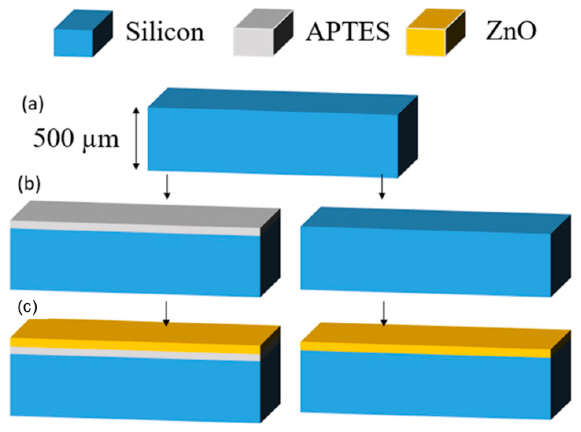
2.5. Microfabrication Processes

Figure 3 shows a schematic of the deposition steps for depositing our ZnO NPs from substrate cleaning to surface treatment to deposition. Three main fabrication steps are presented. Firstly, the substrate chosen for this work was p-type Si cleaned with acetone and piranha (see Section 2.2 for further details). Next, we functionalized one substrate, shown on the left, with a layer of APTES deposited by immersion (see Section 2.3 for further details). The substrate (on the right) was cleaned as described but not functionalized. The EPD of the ZnO NP process was the final processing step for both substrate samples as shown.

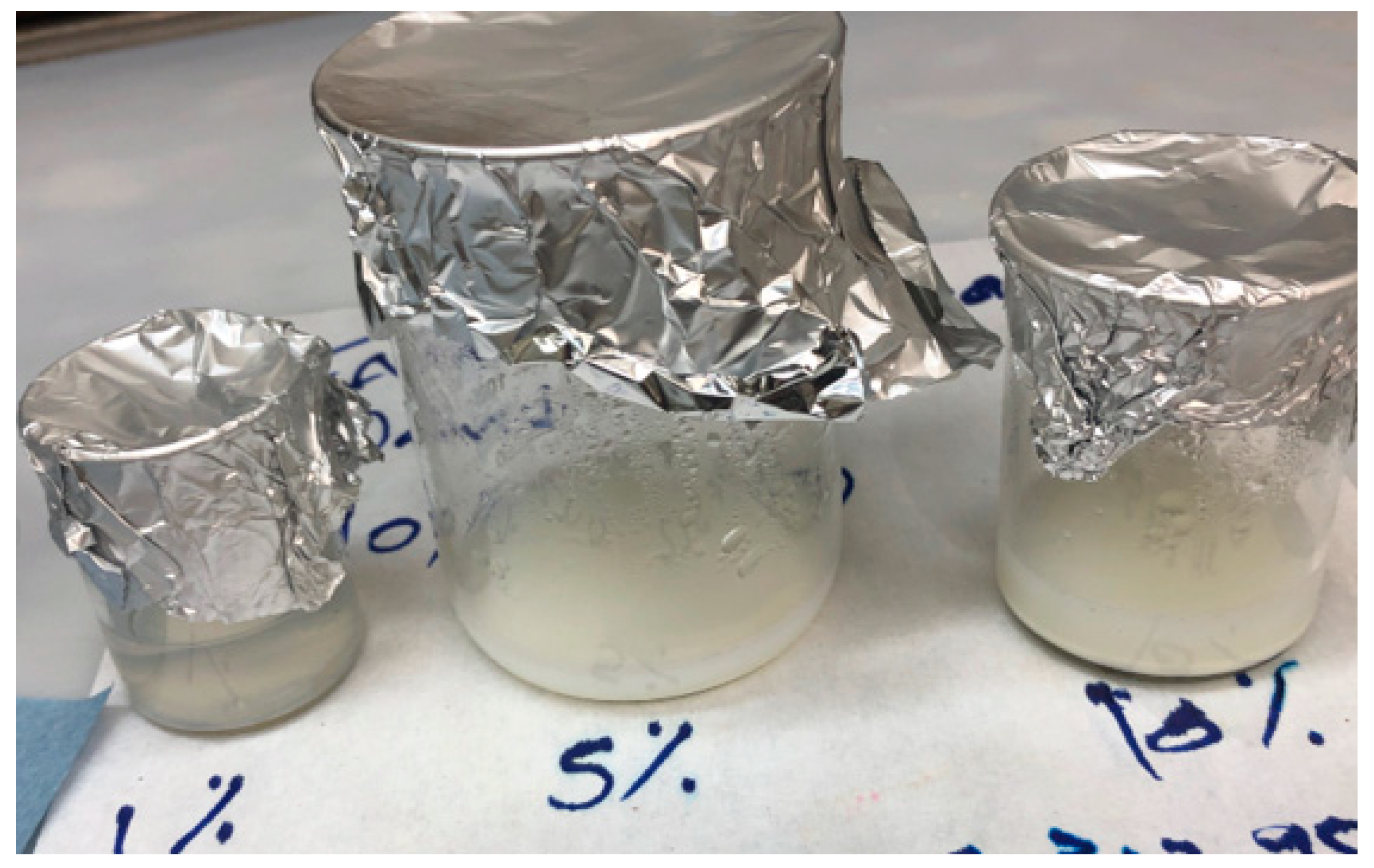
2.6. Synthesizing EPD ZnO Solution

To synthesize the composition of the host solution of ZnO NPs in the EPD system, ZnO NPs were dispersed in a mixture by weight of 10% ethylene glycol, 10% ethanol, and 80% deionized water. The solution was heated at 60 °C while being stirred by a magnetic stirrer (800 rpm) and was then sonicated for 3 h at ambient temperature. This solution was optimized to promote uniform thickness growth on substrates. By controlling the EPD solvent solution, not only might we minimize the structural coffee ring effect but also, we can obtain a higher boiling point of the EPD solvent with minimum surface tension. We used ethylene glycol as a solvent to create a uniform deposition of layered nanoparticles due to offset outward convective flow [27]. This composition was also used by Garcia-Ferrera et al. [22] with the nonionic surfactant Triton X-100. However, in our experiment we studied the growth of different concentrations of ZnO deposited onto Si without the use of a surfactant by EPD (Figure 4).

2.7. ZnO Nanostructure Characterization

We studied the surface morphology by atomic force microscopy (Veeco Dimension 3100 AFM, Gaithersburg, MD, USA), fluorescence emission and excitation spectra of ZnO determined from Fluorolog®-3 spectrofluorometer system by Horiba at an excitation wavelength of 315 nm, and wavelength excitation range 200–600 for excitation and emission.

3. Results

We started our study by optimizing the EPD chemical solutions of ZnO precursor in order to obtain smooth, flat microstructures and surfaces with good electrical characteristics and minimum elastic deformation. Three different concentrations of ZnO were used in this investigation: 1, 5 and 10 wt% of ZnO nanoparticles, where the solvent consisted of ethanol and DI water (see Table 1). A 50 nm and 100 nm BET (Brunauer–Emmett–Teller) instrument was used to study the influence of the nanoparticles’ diameters on the surface morphology and nanoelectronics device performance.

3.1. Fluorescence Spectra for Sensing ZnO Microparticles and Nanoparticles in DI Water

We investigated the impact of particle size on the photoluminescence of ZnO mixed with DI water and the sensitivity of ZnO nanoparticles. We analyzed the fluorolog emission and excitation spectra of the EPD suspension. Figure 1 shows normalized fluorescence emission and excitation spectra of ZnO microparticles mixed with DI water by using a Fluorolog®-3 spectrofluorometer system for a fixed excitation wavelength (λf = 315 nm). The strong intensity emission peak wavelength and the full width at half-maxima (FWHM) are 383 nm (energy equivalent to E peak-ems-micro = 3.2 eV blue range) and 32 nm, respectively. Additionally, there were other weak UV deep-level emissions whose peak wavelength were 355 nm (3.4925 eV) and 337 nm (3.679 eV). On the excitation spectrum, the highest intensity excitation peak wavelength recorded and the full width at half-maxima (FWHM) were 312 nm (energy equivalent to EPeak-ext = 3.9739 eV) and 43 nm, respectively. We obtained the integral over the whole emission spectrum to evaluate the fluorescent quantum yield (FQY) of ZnO NPs immersed in H2O (pure water) which was 0.35. We used the following relationship [48]:
Φ F = 0 F λ f ( λ ) d λ
where ΦF is the fluorescence quantum yield of ZnO and Fλf (λ) is the emission spectrum of ZnO obtained from the Fluorolog®-3 spectrofluorometer system.
Researchers use ΦF to calculate the efficiency of the fluorescence process. There are other methods (relative [49,50,51,52,53,54,55,56] and absolute [51,57,58,59] measurement of quantum yields and the MATLAB [60] toolbox) proposed by several researchers. We used the absolute measurement with standardized procedure mentioned in sample preparation and wavelength [55]. It is worth mentioning that the fluorescence spectrum (emission spectrum) in Figure 5A reflects the ZnO microparticle distribution of the probability of the various transitions from the lowest energy an electron can occupy when it gains energy (photon or phonon) S1 to various energy levels in the ground state (original position of an electron) S0. It illustrates that the probability of an electron transitioning on a wavelength at 383 nm which corresponds to (ENP = 3.24 eV) is the highest on the wavelength spectrum. The calculated energy loss of electrons transitioning from the excited state (excitation spectrum) to the ground state (emission spectrum) is 0.7367 eV by using Strokes shift (wavelength) [61].
Δ λ = λ f λ a
where λf is the maximum wavelength of the fluorescence emission, and λa is the maximum wavelength of the absorbed spectrum.
We repeated the aforementioned processes with ZnO nanoparticle samples immersed in DI water (30 mL) under similar conditions to present a comparison analysis of particle size effects on the ZnO fluorescence spectrum. Figure 5B shows one strong intensity emission peak wavelength, the full width at half-maxima (FWHM), fluorescent quantum yield, and Stroke shift energy are 399 nm (energy equivalent to EPeak-ems-nano = 3.1074 eV (blue range)), 60 nm, 0.5182, and 0.971 eV, respectively. On the excitation spectrum of ZnO NPs, the highest fluorescence intensity excitation peak wavelength recorded and the full width at half-maxima (FWHM) were 304 nm (energy equivalent to EPeak-ext-nano = 4.0784 eV) and 27 nm, respectively. Table 2 shows highlighted results from the emission and excitation spectra of different ZnO particle sizes.
We explain the observed emission mechanisms of ZnO NP fluorescence as the following. The 399 nm (3.1 eV) ultraviolent range emission might relate to the inter-band radiation sequence of photogenerated electrons and holes. Typically, light is emitted by an electron carry energy equal to or slightly higher than the direct bandgap energy. According to Li et al. [62], the fluorescence emissions of ZnO quantum dots, synthesized at the [LiOH]/[Zn21] ratio of 1:3 and dispersed in water, were 525 nm (less than ZnO energy bandgap emission) with low intensity (fraction of 104) when it was excited by UV light at 302 nm. A fluorescence emission with energy higher than the bandgap was reported. Zhang et al. [63] deposited ZnO films by using a sputtering system onto an Si substrate and reported a 290 nm emission peak.
In Figure 5C,D, we highlighted the differences of the waveform patterns of ZnO nanoparticles and microparticles. Our observation is that smaller particle sizes of ZnO will increase the energy emission for fluorescence transmission, eliminate several peak emissions, obtain higher FQY efficiency, and require less excitation energy. Although ZnO particles do not show remarkable changes from the water Raman emission peak, the possibility of controllable peak emission shifting, and higher fluorescence, is greater when using ZnO.
The results in Table 2 show, in general, a greater sensitivity of ZnO NPs in fluorolog detection, particularly in the emission peak wavelength, fluorescence quantum yield, and Stokes shift, as compared to the other ZnO microparticles, highlighting the role of ZnO particle sizes in attaining strong emission and excitation spectrum.
When the fluorescence-based sensitivities of ZnO NPs and ZnO µPs are compared, a higher sensory response to the fluorolog spectrum is found for ZnO NPs; for peak wavelength emission, the results also slightly favor the ZnO NPs sensors, while for the emission energy a higher energy (3.24 eV) was observed for ZnO µPs. A higher Stoke shift was observed for ZnO NPs, compared to the ZnO µPs, which can also be seen from the inset of Table 2.
A photoluminescence emission of light with energy larger than the bandgap has also been observed. For instance, sputtering deposition and pulsed laser deposition of ZnO films with a 290 nm and 302 nm wavelengths emissions by Zhang et al. [63] and Ohshima et al. [64], respectively. In this study, high-energy photoemission can be explained as quasi-Fermi level shifts in the conduction band, which is explained by ZnO being an intrinsically n-type material [65].

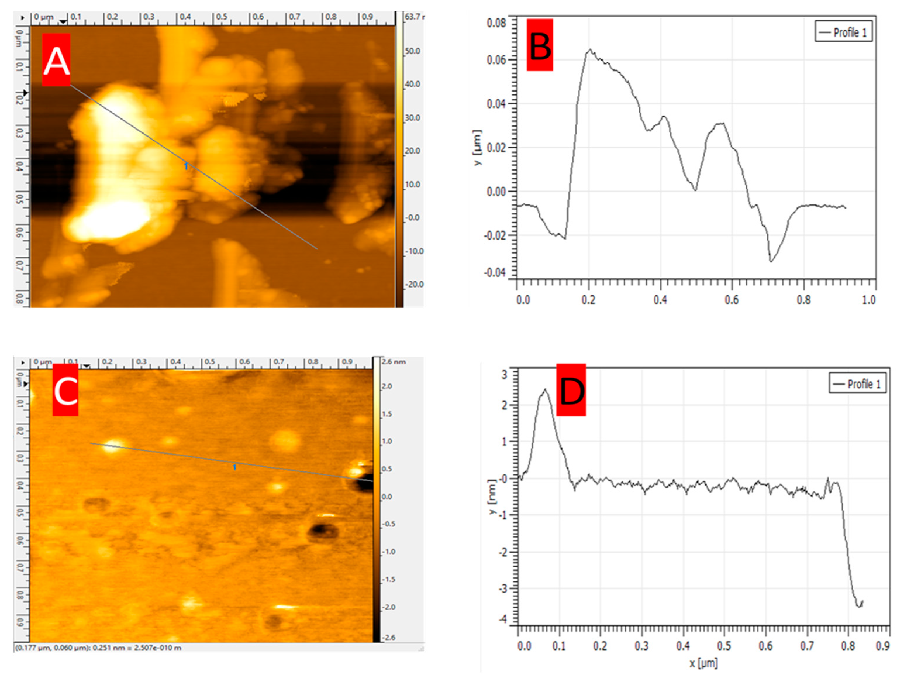
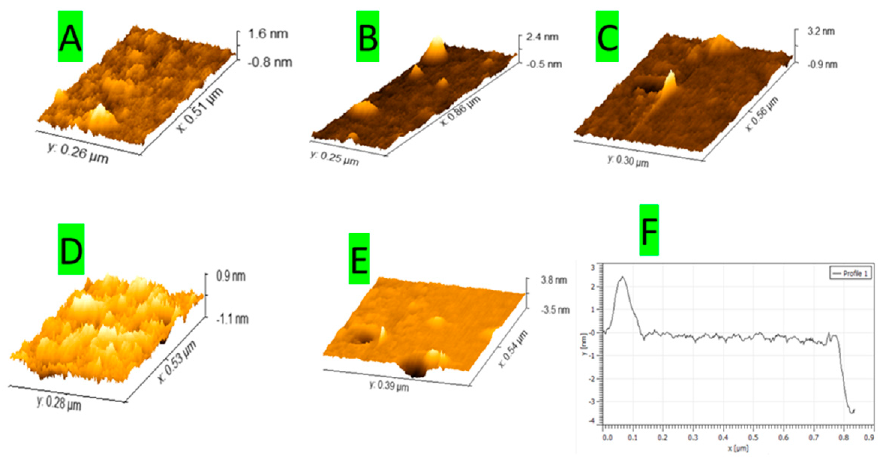
3.2. Atomic Force Microscopy Charachtrization of EPD ZnO on p-Type Si

The comprehensive morphology and surface roughness results of voltage controlled EPD ZnO NP films were analyzed by Veeco Dimension 3100 atomic force microscopy (AFM). The AFM images were taken from five different samples, and we standardized the scanning area to be 1 × 2 μm. Figure 6A–D indicate the 2D AFM measures acquired for the ZnO NP structures with different applied voltages (0–60 V) and surface functionalization of p-silicon substrates. The outcomes show that variation of applied voltage deposition of the EPD ZnO NP system strongly influences the morphology, uniformity, and roughness characterization of the ZnO nanostructure. The AFM graph (Figure 6A) showed limited uniform distribution of a ZnO grain structure, high roughness ratio, and high ZnO concentration in the central area. The AFM surface profile (Figure 6B) showed that roughness dramatically changes from 0 to 1 µm surface area between 62 nm and −24 nm. It is important to mention that the negative sign of thickness-level means that there was a hole with respect to the reference surface level that was chosen automatically by AFM. On the AFM micrograph (Figure 6C), however, we observed a better uniform distribution with minimum grains of a ZnO structure, which was steady with a high-quality ZnO thin film nanostructure with minimum pin-hole structures, and a smooth and crack-free surface [66,67]. The surface profile (Figure 6D), for the blue line on Figure 6C, shows a successful uniformity rate of the EPD system with minimum granular structures, which indicates the influence of applying higher voltage and using functionalized silicon surfaces. The hole at the edge (0.8 µm) of the surface area indicates that the increased thickness with 60 V applied voltage was 4 nm thicker on average.
Figure 7A–F shows 3D images of EPD ZnO nanoparticles on p-type silicon samples and the influence of applying different EPD voltages. When the applied EPD system voltage increased in the EPD solution from 5 to 60 V, the average thicknesses of the thin film on the p-type substrate were also increased. Figure 7A–F also shows that when a higher voltage was applied on the ZnO thin film, the overall surface roughness and surface uniformity increased. The surface structure associated with 60 V (Figure 7C) was smoother than 10 V EPD applied voltage (Figure 7A) with fewer grains on the surface and less ZnO NP agglomeration. The grain size and thickness increased as the applied voltage increased. Thus, an increase in the EPD applied voltage on the ZnO NPs surface improves the overall crystalline structure of deposited ZnO NPs on P-type silicon substrates. This is confirmed by the AFM analysis. The improved uniformity with applied voltage may be due to the increase in zeta potential in the EPD setup which leads to a higher diffusivity of ZnO particles in the EPD solution [45,68]. The formation of a large island structure associated with higher applied voltage may be due to the EPD ZnO NPs, which coalesced with the bipolar ZnO thin film. Figure 7D shows the influence of depositing a heated APTES layer as a functionalization surface layer on bare p-type silicon substrates before depositing a ZnO layer. We observed that APTES-treated surfaces showed better results in terms of uniformity, fewer grains, and controllable ZnO thickness. With increasing the grain size, the surface of the thin structures on p-type silicon substrate formed island-shaped structures that led to rougher surfaces [69,70].

4. Discussion

In this communication, our present investigation has demonstrated that morphology controlled ZnO nanoparticles (NPs) can be successfully deposited via a system of electronic deposition with synthesized organic solvent as the EPD solution and be exploited as fluorescence-based sensors for the detection of ZnO particle sizes. This study was carried out through synthesizing EPD solvent, microfabricating samples, functionalizing substrates, characterizing with fluorologs and AFM, and sensing particle sizes via fluorolog spectra. The fluorolog photoluminescence properties of the ZnO NPs and microparticles mixed with DI water highly influence the energy emission for fluorescence transmission, eliminate several peak emissions, obtain higher FQY efficiency, and require less excitation energy. Hence, compared with other EPD solutions, ZnO NP surfaces synthesized by using a minimum surface tension solvent such as ethylene glycol obtain a better-quality grain size, higher transmittance of fluorescent emission associated with small particle sizes, and better crystallite quality. It was observed that there was a strong influence of the applied voltage, ZnO concentration, and APTES-treated substrates on the overall morphology, coverage, thickness, and flatness of deposited nanostructures. We observed that APTES-treated surfaces showed better results in terms of uniformity, fewer grains, and controllable ZnO thickness. We showed that increasing the EPD applied voltage can improve the coverage, adhesion, and the uniformity of ZnO NP nanostructures. Our work in this direction will focus on reproducibility tests, depositing ZnO NPs onto p-type doped direct bandgap semiconductors, such as GaAs, as well as sapphire substrates to test the performance of ZnO/substrate heterojunctions. We will take current–voltage characteristics of our current samples. Other experimental possibilities include introducing channels in our substrates by using lithography to ensure the accumulation of ZnO nanoparticles in designated areas and examining our samples by atomic force microscopy (AFM) to study sample topology. We will also experiment with introducing variation to the EPD system via changing the distance between electrodes, length of contact with electrolytes, electrode materials, and electrolyte composition. A device performance study based on the EPD of ZnO on p-silicon is also in progress.

5. Conclusions

APTES functionalized silicon surfaces perform better with EPD of ZnO NPs than non-functionalized substrates in terms of adhesion, uniformity, and surface roughness. We used the fluorolog properties for distinguishing and sensing the ZnO particle sizes. The energy emission was highly influenced by the ZnO particle size. The results obtained can enhance the integration of EPD of ZnO NPs in the microfabrication of sensors, materials for nano electronics devices, and thin film transistors (TFTs), where ZnO NPs improve the reliability, affordability, and increased sensitivity needed for the next generation of nanoscale devices and systems.

Author Contributions

Conceptualization, T.D.-R.; data curation, F.H.; formal analysis, F.H.; funding acquisition, T.D.-R.; investigation, T.D.-R.; methodology, T.D.-R.; project administration, T.D.-R.; resources, A.Y., C.O. and T.D.-R.; software, T.D.-R.; supervision, T.D.-R.; validation, T.D.-R.; writing—original draft, F.H.; writing—review and editing, T.D.-R. All authors have read and agreed to the published version of the manuscript.

Funding

This work was partially funded by the Louisiana Board of Regents LIFT2 grant (LSU-2018-LIFT 002) and the LSU Foundation project #104454-340 as created through the generosity of Dr. Kristina M. Johnson.

Institutional Review Board Statement

Not applicable.

Informed Consent Statement

Not applicable.

Data Availability Statement

Data sharing not applicable.

Acknowledgments

The authors also wish to recognize the staff and appreciate the use of the Electronic Materials & Devices Laboratory (EMDL) housed in the Division of Electrical & Computer Engineering at Louisiana State University.

Conflicts of Interest

The authors declare no conflict of interest.

References

  1. Chaudhary, S.; Umar, A.; Bhasin, K.K.; Baskoutas, S. Chemical Sensing Applications of Zno Nanomaterials. Materials 2018, 11, 287. [Google Scholar] [CrossRef] [PubMed] [Green Version]
  2. Priyadarsini, S.; Mohanty, S.; Mukherjee, S.; Basu, S.; Mishra, M. Graphene and Graphene Oxide as Nanomaterials for Medicine and Biology Application. J. Nanostruct. Chem. 2018, 8, 123–137. [Google Scholar] [CrossRef] [Green Version]
  3. Wang, J.; Chen, R.; Xiang, L.; Komarneni, S. Synthesis, Properties and Applications of Zno Nanomaterials with Oxygen Vacancies: A Review. Ceram. Int. 2018, 44, 7357–7377. [Google Scholar] [CrossRef]
  4. Wang, X.; Yu, S.; Jin, J.; Wang, H.; Alharbi, N.S.; Alsaedi, A.; Hayat, T.; Wang, X. Application of Graphene Oxides and Graphene Oxide-Based Nanomaterials in Radionuclide Removal from Aqueous Solutions. Sci. Bull. 2016, 61, 1583–1593. [Google Scholar] [CrossRef] [Green Version]
  5. Wu, Z.P.; Wang, Y.; Liu, X.; Lv, C.; Li, Y.; Wei, D.; Liu, Z. Carbon-Nanomaterial-Based Flexible Batteries for Wearable Electronics. Adv. Mater. 2019, 31, 1800716. [Google Scholar] [CrossRef] [PubMed]
  6. Zeng, H.; Duan, G.; Li, Y.; Yang, S.; Xu, X.; Cai, W. Blue Luminescence of Zno Nanoparticles Based on Non-Equilibrium Processes: Defect Origins and Emission Controls. Adv. Funct. Mater. 2010, 20, 561–572. [Google Scholar] [CrossRef]
  7. Tachikawa, S.; Noguchi, A.; Tsuge, T.; Hara, M.; Odawara, O.; Wada, H. Optical Properties of Zno Nanoparticles Capped with Polymers. Materials 2011, 4, 1132–1143. [Google Scholar] [CrossRef] [Green Version]
  8. Dagdeviren, C.; Hwang, S.-W.; Su, Y.; Kim, S.; Cheng, H.; Gur, O.; Haney, R.; Omenetto, F.G.; Huang, Y.; Rogers, J.A. Transient, Biocompatible Electronics and Energy Harvesters Based on Zno. Small 2013, 9, 3398–3404. [Google Scholar] [CrossRef]
  9. Franco, A., Jr.; Pessoni, H. Effect of Gd Doping on the Structural, Optical Band-Gap, Dielectric and Magnetic Properties of Zno Nanoparticles. Phys. B Condens. Matter 2017, 506, 145–151. [Google Scholar] [CrossRef]
  10. Zhang, Y.; Wen, Y.-H.; Zheng, J.-C.; Zhu, Z.-Z. Direct to Indirect Band Gap Transition in Ultrathin Zno Nanowires under Uniaxial Compression. Appl. Phys. Lett. 2009, 94, 113114. [Google Scholar] [CrossRef]
  11. Srikant, V.; Clarke, D.R. On the Optical Band Gap of Zinc Oxide. J. Appl. Phys. 1998, 83, 5447–5451. [Google Scholar] [CrossRef]
  12. Wang, J.; Sun, X.W.; Wei, A.; Lei, Y.; Cai, X.; Li, C.M.; Dong, Z.L. Zinc Oxide Nanocomb Biosensor for Glucose Detection. Appl. Phys. Lett. 2006, 88, 233106. [Google Scholar] [CrossRef]
  13. Arya, S.K.; Saha, S.; Ramirez-Vick, J.E.; Gupta, V.; Bhansali, S.; Singh, S.P. Recent Advances in Zno Nanostructures and Thin Films for Biosensor Applications. Anal. Chim. Acta 2012, 737, 1–21. [Google Scholar] [CrossRef] [PubMed]
  14. Wei, A.; Sun, X.W.; Wang, J.; Lei, Y.; Cai, X.; Li, C.M.; Dong, Z.; Huang, W. Enzymatic Glucose Biosensor Based on Zno Nanorod Array Grown by Hydrothermal Decomposition. Appl. Phys. Lett. 2006, 89, 123902. [Google Scholar] [CrossRef]
  15. Hassan, H.S.; Elkady, M.; Farghali, A.; Salem, A.M.; El-Hamid, A.A. Fabrication of Novel Magnetic Zinc Oxide Cellulose Acetate Hybrid Nano-Fiber to Be Utilized for Phenol Decontamination. J. Taiwan Inst. Chem. Eng. 2017, 78, 307–316. [Google Scholar] [CrossRef]
  16. Yadav, A.; Yadav, B. A Mechanochemical Synthesis of Nanostructured Zinc Oxide Via Acetate Route for Lpg Sensing. J. Exp. Nanosci. 2014, 9, 501–511. [Google Scholar] [CrossRef]
  17. Tonto, P.; Mekasuwandumrong, O.; Phatanasri, S.; Pavarajarn, V.; Praserthdam, P. Preparation of Zno Nanorod by Solvothermal Reaction of Zinc Acetate in Various Alcohols. Ceram. Int. 2008, 34, 57–62. [Google Scholar] [CrossRef]
  18. Ohyama, M.; Kouzuka, H.; Yoko, T. Sol-Gel Preparation of Zno Films with Extremely Preferred Orientation Along (002) Plane from Zinc Acetate Solution. Thin Solid Film. 1997, 306, 78–85. [Google Scholar] [CrossRef]
  19. Sakohara, S.; Ishida, M.; Anderson, M.A. Visible Luminescence and Surface Properties of Nanosized Zno Colloids Prepared by Hydrolyzing Zinc Acetate. J. Phys. Chem. B 1998, 102, 10169–10175. [Google Scholar] [CrossRef]
  20. Belhaj, M.; Dridi, C.; Elhouichet, H.; Valmalette, J.C. Study of Zno Nanoparticles Based Hybrid Nanocomposites for Optoelectronic Applications. J. Appl. Phys. 2016, 119, 095501. [Google Scholar] [CrossRef]
  21. Lai, L.-T.; Chang, S.-J.; Yang, C.-C.; Young, S.-J. Uv-Enhanced 2-D Nanostructured Zno Field Emitter with Adsorbed Pt Nanoparticles. IEEE Electron Device Lett. 2018, 39, 1932–1935. [Google Scholar] [CrossRef]
  22. Zhang, Q.; Xie, G.; Xu, M.; Su, Y.; Tai, H.; Du, H.; Jiang, Y. Visible Light-Assisted Room Temperature Gas Sensing with Zno-Ag Heterostructure Nanoparticles. Sens. Actuators B Chem. 2018, 259, 269–281. [Google Scholar] [CrossRef]
  23. Lin, C.-H.; Chang, S.-J.; Chen, W.-S.; Hsueh, T.-J. Transparent Zno-Nanowire-Based Device for Uv Light Detection and Ethanol Gas Sensing on C-Si Solar Cell. RSC Adv. 2016, 6, 11146–11150. [Google Scholar] [CrossRef]
  24. Zhu, L.; Zeng, W. Room-Temperature Gas Sensing of Zno-Based Gas Sensor: A Review. Sens. Actuators A Phys. 2017, 267, 242–261. [Google Scholar] [CrossRef]
  25. Comini, E.; Hartiti, B.; Moumen, A.; Arachchige, H.M.M.; Fadili, S.; Thevenin, P.; Kamal, A. Effect of Vanadium Doping on Zno Sensing Properties Synthesized by Spray Pyrolysis. Mater. Des. 2018, 139, 56–64. [Google Scholar]
  26. Fan, Z.; Wang, D.; Chang, P.-C.; Tseng, W.-Y.; Lu, J.G. Zno Nanowire Field-Effect Transistor and Oxygen Sensing Property. Appl. Phys. Lett. 2004, 85, 5923–5925. [Google Scholar] [CrossRef] [Green Version]
  27. Li, X.; Chang, Y.; Long, Y. Influence of Sn Doping on Zno Sensing Properties for Ethanol and Acetone. Mater. Sci. Eng. C 2012, 32, 817–821. [Google Scholar] [CrossRef]
  28. Miura, N.; Akisada, K.; Wang, J.; Zhuiykov, S.; Ono, T. Mixed-Potential-Type No X Sensor Based on Ysz and Zinc Oxide Sensing Electrode. Ionics 2004, 10, 1–9. [Google Scholar] [CrossRef]
  29. Wan, Q.; Li, Q.; Chen, Y.; Wang, T.-H.; He, X.; Li, J.; Lin, C. Fabrication and Ethanol Sensing Characteristics of Zno Nanowire Gas Sensors. Appl. Phys. Lett. 2004, 84, 3654–3656. [Google Scholar] [CrossRef] [Green Version]
  30. Yang, K.; She, G.-W.; Wang, H.; Ou, X.-M.; Zhang, X.-H.; Lee, C.-S.; Lee, S.-T. Zno Nanotube Arrays as Biosensors for Glucose. J. Phys. Chem. C 2009, 113, 20169–20172. [Google Scholar] [CrossRef]
  31. Zhao, Z.; Lei, W.; Zhang, X.; Wang, B.; Jiang, H. Zno-Based Amperometric Enzyme Biosensors. Sensors 2010, 10, 1216–1231. [Google Scholar] [CrossRef] [PubMed]
  32. Singh, S.; Arya, S.K.; Pandey, P.; Malhotra, B.; Saha, S.; Sreenivas, K.; Gupta, V. Cholesterol Biosensor Based on Rf Sputtered Zinc Oxide Nanoporous Thin Film. Appl. Phys. Lett. 2007, 91, 063901. [Google Scholar] [CrossRef]
  33. Lim, S.; Kwon, S.; Kim, H. Zno Thin Films Prepared by Atomic Layer Deposition and Rf Sputtering as an Active Layer for Thin Film Transistor. Thin Solid Film. 2008, 516, 1523–1528. [Google Scholar] [CrossRef]
  34. Kwon, S.; Bang, S.; Lee, S.; Jeon, S.; Jeong, W.; Kim, H.; Gong, S.C.; Chang, H.J.; Park, H.-H.; Jeon, H. Characteristics of the Zno Thin Film Transistor by Atomic Layer Deposition at Various Temperatures. Semicond. Sci. Technol. 2009, 24, 035015. [Google Scholar] [CrossRef]
  35. Lim, S.; Kwon, S.-J.; Kim, H.; Park, J.-S. High Performance Thin Film Transistor with Low Temperature Atomic Layer Deposition Nitrogen-Doped Zno. Appl. Phys. Lett. 2007, 91, 183517. [Google Scholar] [CrossRef] [Green Version]
  36. Siddiqui, J.; Cagin, E.; Chen, D.; Phillips, J. Zno Thin-Film Transistors with Polycrystalline (Ba, Sr) Ti O 3 Gate Insulators. Appl. Phys. Lett. 2006, 88, 212903. [Google Scholar] [CrossRef] [Green Version]
  37. Chen, H.-C.; Peng, G.-T.; Liu, T.-F. Optoelectronic Properties and Anisotropic Stress of Mo: Zno Thin Films Deposited on Flexible Substrates by Radio Frequency Magnetron Sputtering. Appl. Opt. 2020, 59, 1454–1460. [Google Scholar] [CrossRef]
  38. Kaur, G.; Mitra, A.; Yadav, K. Pulsed Laser Deposited Al-Doped Zno Thin Films for Optical Applications. Prog. Nat. Sci. Mater. Int. 2015, 25, 12–21. [Google Scholar] [CrossRef] [Green Version]
  39. Robbins, J.; Harvey, J.; Leaf, J.; Fry, C.; Wolden, C. Transport Phenomena in High Performance Nanocrystalline Zno: Ga Films Deposited by Plasma-Enhanced Chemical Vapor Deposition. Thin Solid Film. 2005, 473, 35–40. [Google Scholar] [CrossRef]
  40. Tan, S.T.; Chen, B.; Sun, X.; Fan, W.; Kwok, H.S.; Zhang, X.; Chua, S. Blueshift of Optical Band Gap in Zno Thin Films Grown by Metal-Organic Chemical-Vapor Deposition. J. Appl. Phys. 2005, 98, 013505. [Google Scholar] [CrossRef] [Green Version]
  41. Khan, M.; Bhatti, K.; Qindeel, R.; Alonizan, N.; Althobaiti, H.S. Characterizations of Multilayer Zno Thin Films Deposited by Sol-Gel Spin Coating Technique. Results Phys. 2017, 7, 651–655. [Google Scholar] [CrossRef]
  42. Coke, M. Electronic Properties of Zinc Oxide and Related Materials Grown by Molecular Beam Epitaxy; UCL (University College London): London, UK, 2017. [Google Scholar]
  43. Banerjee, P.; Lee, W.-J.; Bae, K.-R.; Lee, S.B.; Rubloff, G.W. Structural, Electrical, and Optical Properties of Atomic Layer Deposition Al-Doped Zno Films. J. Appl. Phys. 2010, 108, 043504. [Google Scholar] [CrossRef] [Green Version]
  44. Hu, L.; Hecht, D.S.; Gruner, G. Carbon Nanotube Thin Films: Fabrication, Properties, and Applications. Chem. Rev. 2010, 110, 5790–5844. [Google Scholar] [CrossRef] [PubMed]
  45. Kanakamedala, K.; DeSoto, J.; Sarkar, A.; Race, T.D. Study of Electrospray Assisted Electrophoretic Deposition of Carbon Nanotubes on Insulator Substrates. Electron. Mater. Lett. 2015, 11, 949–956. [Google Scholar] [CrossRef]
  46. Maulik, S.; Sarkar, A.; Basu, S.; Daniels-Race, T. Voltage-Controlled Spray Deposition of Multiwalled Carbon Nanotubes on Semiconducting and Insulating Substrates. J. Electron. Mater. 2018, 47, 4604–4609. [Google Scholar] [CrossRef]
  47. Sarkar, A.; Daniels-Race, T. Electrophoretic Deposition of Carbon Nanotubes on 3-Amino-Propyl-Triethoxysilane (Aptes) Surface Functionalized Silicon Substrates. Nanomaterials 2013, 3, 272–288. [Google Scholar] [CrossRef] [PubMed] [Green Version]
  48. Valeur, B. Molecular Fluorescence. Digit. Encycl. Appl. Phys. 2003, 477–531. [Google Scholar] [CrossRef]
  49. Cosby, A.G.; Quevedo, G.; Boros, E. A High-Throughput Method to Measure Relative Quantum Yield of Lanthanide Complexes for Bioimaging. Inorg. Chem. 2019, 58, 10611–10615. [Google Scholar] [CrossRef]
  50. Levitus, M. Tutorial: Measurement of Fluorescence Spectra and Determination of Relative Fluorescence Quantum Yields of Transparent Samples. Methods Appl. Fluoresc. 2020, 8, 033001. [Google Scholar] [CrossRef]
  51. Magde, D.; Wong, R.; Seybold, P.G. Fluorescence Quantum Yields and Their Relation to Lifetimes of Rhodamine 6g and Fluorescein in Nine Solvents: Improved Absolute Standards for Quantum Yields. Photochem. Photobiol. 2002, 75, 327–334. [Google Scholar] [CrossRef]
  52. Serpone, N. Relative Photonic Efficiencies and Quantum Yields in Heterogeneous Photocatalysis. J. Photochem. Photobiol. A Chem. 1997, 104, 1–12. [Google Scholar] [CrossRef]
  53. Ware, W.R.; Rothman, W. Relative Fluorescence Quantum Yields Using an Integrating Sphere. The Quantum Yield of 9, 10-Diphenylanthracene in Cyclohexane. Chem. Phys. Lett. 1976, 39, 449–453. [Google Scholar]
  54. Williams, A.T.R.; Winfield, S.A.; Miller, J.N. Relative Fluorescence Quantum Yields Using a Computer-Controlled Luminescence Spectrometer. Analyst 1983, 108, 1067–1071. [Google Scholar] [CrossRef]
  55. Würth, C.; Grabolle, M.; Pauli, J.; Spieles, M.; Resch-Genger, U. Relative and Absolute Determination of Fluorescence Quantum Yields of Transparent Samples. Nat. Protoc. 2013, 8, 1535–1550. [Google Scholar] [CrossRef] [PubMed]
  56. Würth, C.; Grabolle, M.; Pauli, J.; Spieles, M.; Resch-Genger, U. Comparison of Methods and Achievable Uncertainties for the Relative and Absolute Measurement of Photoluminescence Quantum Yields. Anal. Chem. 2011, 83, 3431–3439. [Google Scholar] [CrossRef]
  57. Meijer, M.S.; Rojas-Gutierrez, P.A.; Busko, D.; Howard, I.A.; Frenzel, F.; Würth, C.; Resch-Genger, U.; Richards, B.S.; Turshatov, A.; Capobianco, J.A. Absolute Upconversion Quantum Yields of Blue-Emitting Liyf 4: Yb 3+, Tm 3+ Upconverting Nanoparticles. Phys. Chem. Chem. Phys. 2018, 20, 22556–22562. [Google Scholar] [CrossRef] [Green Version]
  58. Porres, L.; Holland, A.; Pålsson, L.-O.; Monkman, A.P.; Kemp, C.; Beeby, A. Absolute Measurements of Photoluminescence Quantum Yields of Solutions Using an Integrating Sphere. J. Fluoresc. 2006, 16, 267–273. [Google Scholar] [CrossRef] [PubMed]
  59. Würth, C.; Kaiser, M.; Wilhelm, S.; Grauel, B.; Hirsch, T.; Resch-Genger, U. Excitation Power Dependent Population Pathways and Absolute Quantum Yields of Upconversion Nanoparticles in Different Solvents. Nanoscale 2017, 9, 4283–4294. [Google Scholar] [CrossRef] [PubMed]
  60. Wünsch, U.J.; Murphy, K.R.; Stedmon, C.A. Fluorescence Quantum Yields of Natural Organic Matter and Organic Compounds: Implications for the Fluorescence-Based Interpretation of Organic Matter Composition. Front. Mar. Sci. 2015, 2, 98. [Google Scholar] [CrossRef]
  61. McCartney, M.; Whitaker, A.; Wood, A. George Gabriel Stokes: Life, Science and Faith; Oxford University Press: New York, NC, USA, 2019. [Google Scholar]
  62. Li, S.; Sun, Z.; Li, R.; Dong, M.; Zhang, L.; Qi, W.; Zhang, X.; Wang, H. Zno Nanocomposites Modified by Hydrophobic and Hydrophilic Silanes with Dramatically Enhanced Tunable Fluorescence and Aqueous Ultrastability toward Biological Imaging Applications. Sci. Rep. 2015, 5, 8475. [Google Scholar] [CrossRef] [Green Version]
  63. Guo-Bin, Z.; Chao-Shu, S.; Zheng-Fu, H.; Jun-Yan, S.; Zhu-Xi, F.; Kirm, M.; Zimmerer, G. Photoluminescent Properties of Zno Films Deposited on Si Substrates. Chin. Phys. Lett. 2001, 18, 441. [Google Scholar] [CrossRef]
  64. Ohshima, T.; Thareja, R.; Yamagata, Y.; Ikegami, T.; Ebihara, K.; Narayan, J. Laser-Ablated Plasma for Deposition of Zno Thin Films on Various Substrates. Sci. Technol. Adv. Mater. 2001, 2, 517–523. [Google Scholar] [CrossRef] [Green Version]
  65. Zhang, S.; Wei, S.-H.; Zunger, A. Intrinsic N-Type Versus P-Type Doping Asymmetry and the Defect Physics of Zno. Phys. Rev. B 2001, 63, 075205. [Google Scholar] [CrossRef] [Green Version]
  66. Foo, K.L.; Kashif, M.; Hashim, U.; Liu, W.-W. Effect of Different Solvents on the Structural and Optical Properties of Zinc Oxide Thin Films for Optoelectronic Applications. Ceram. Int. 2014, 40, 753–761. [Google Scholar] [CrossRef]
  67. Sengupta, J.; Sahoo, R.; Mukherjee, C. Effect of Annealing on the Structural, Topographical and Optical Properties of Sol–Gel Derived Zno and Azo Thin Films. Mater. Lett. 2012, 83, 84–87. [Google Scholar] [CrossRef] [Green Version]
  68. Besra, L.; Liu, M. A Review on Fundamentals and Applications of Electrophoretic Deposition (Epd). Prog. Mater. Sci. 2007, 52, 1–61. [Google Scholar]
  69. Kim, Y.Y.; Kong, B.H.; Cho, H.K. Vertically Arrayed Ga-Doped Zno Nanorods Grown by Magnetron Sputtering: The Effect of Ga Contents and Microstructural Evaluation. J. Cryst. Growth 2011, 330, 17–21. [Google Scholar] [CrossRef]
  70. Lee, S.M.; Ikeda, S.; Yagi, T.; Harada, T.; Ennaoui, A.; Matsumura, M. Fabrication of Cuins 2 Films from Electrodeposited Cu/in Bilayers: Effects of Preheat Treatment on Their Structural, Photoelectrochemical and Solar Cell Properties. Phys. Chem. Chem. Phys. 2011, 13, 6662–6669. [Google Scholar] [CrossRef]
Figure 1. Schematic diagram of the EPD system set-up: 1—DC voltage source; 2—EPD ZnO solution; 3—Platinum (2 × 1 cm2 electrode); 4-silicon substrate; 5—connectors; 6—EPD base; 7—adjustable contact length of electrodes within the electrolyte; 8—adjustable distance between electrode and substrate.
Chemosensors 09 00005 g001
Figure 2. (a) Cleaned silicon sample and platinum sample (electrode). (b) ZnO nanopowder as-purchased from Sigma-Aldrich (catalog number 677450). (c) Substrate treated by warm piranha solution and (d) Silicon substrate treated by APTES solution prepared for ZnO electrophoretic deposition.
Chemosensors 09 00005 g002
Figure 3. Three fabrication steps (ac) from cleaning to depositing ZnO NPs by electrophoretic deposition.
Chemosensors 09 00005 g003
Figure 4. After heating while magnetic stirring, and then sonication of the three different ZnO concentrations.
Chemosensors 09 00005 g004
Figure 5. (A) microparticles emission and excitation spectrum of ZnO, (B) ZnO NPs emission and excitation spectrum, (C) ZnO particle size fluorescent emission contrast, and (D) ZnO particle size fluorescent excitation contrast.
Chemosensors 09 00005 g005
Figure 6. Structure study of electrophoretic deposited ZnO NPs. We examined the surface uniformity and roughness by atomic force microscopy (AFM). 2D AFM images of the ZnO thin films EPD with different applied voltage: (A) 10 V; (B) Surface profile of the blue line on (A); (C) 60 V with APTES; and (D) Surface profile of the blue line on (C).
Chemosensors 09 00005 g006
Figure 7. AFM 3D thickness measurements of ZnO structures with different applied voltage EPD system. ZnO surfaces deposited with different voltages: (A) 10 V; (B) 30 V; (C) 60 V; (D) APTES functionalized substrate with 10 V; (E) APTES functionalized substrate with 60 V; and (F) thickness profile of (E).
Chemosensors 09 00005 g007
Table 1. Description of EPD solution samples used.
Zinc Weight Percentage to EPD Solution (%)C2H6O2 Weight Percentage to EPD Solution (%)DI Water Weight Percentage to EPD Solution (%)Average Particle Diameter (nm)
1 (0.22 g)198050
5 (1.1 g)158050
10 (2.2 g)108050
10 (2.2 g)1080100
Table 2. Summary of ZnO NPs fluorescence of EPD solution samples. Fluorescence spectrometer of ZnO particles immersed in DI water under fixed wavelength (λ = 315 nm).
EmissionExcitationStoke Shift
Point of StudyPeak Wavelength (nm)Energy (eV)FWHM (nm)FQYPeak Wavelength (nm)Energy (eV)FWHM (nm)Energy (eV)
Particles Sizes
ZnO nanoparticles3993.10600.523044.08270.971
ZnO microparticles3833.24320.353123.98430.74
Publisher’s Note: MDPI stays neutral with regard to jurisdictional claims in published maps and institutional affiliations.

