Article

Gold Nanoframe Array Electrode for Straightforward Detection of Hydrogen Peroxide

by
Agnes Purwidyantri
1,2,
Ya-Chung Tian
3,
Gardin Muhammad Andika Saputra
4,
Briliant Adhi Prabowo
1,5,
Hui-Ling Liu
6,
Chia-Ming Yang
6,7,8,9,* and
Chao-Sung Lai
3,6,8,10,11,*
1
International Iberian Nanotechnology Laboratory, 4715-330 Braga, Portugal
2
Research Unit for Clean Technology, Indonesian Institute of Sciences, Bandung 40135, Indonesia
3
Department of Nephrology, Chang Gung Memorial Hospital, Linkou 33305, Taiwan
4
Materials Engineering Department, Faculty of Mechanical and Aerospace Engineering, Bandung Institute of Technology, Bandung 40135, Indonesia
5
Research Center for Electronics and Telecommunications, Indonesian Institute of Sciences, Bandung 40135, Indonesia
6
Department of Electronic Engineering, Chang Gung University, Taoyuan 30002, Taiwan
7
Institute of Electro-Optical Engineering, Chang Gung University, Taoyuan 33302, Taiwan
8
Biosensor Group, Biomedical Engineering Research Center, Chang Gung University, Taoyuan 33302, Taiwan
9
Department of General Surgery, Chang Gung Memorial Hospital, Linkou 33305, Taiwan
10
Department of Materials Engineering, Ming Chi University of Technology, New Taipei City 24301, Taiwan
11
Artificial Intelligence Research Center, Chang Gung University, Taoyuan 30002, Taiwan
*
Authors to whom correspondence should be addressed.
Submission received: 24 December 2020 / Revised: 5 February 2021 / Accepted: 14 February 2021 / Published: 16 February 2021

Abstract

:
The nanostructuring of a sensing membrane is performed through colloidal nanosphere lithography (NSL) techniques with a tiny polystyrene nanobead template 100 nm in size. The solvent ratio adjustment has been proven to be effective in assisting the monolayer deposition of small templating particles with minimal defects. Two distinct structures, namely, a billowy gold nanostructure (BGN) where the nanobead template is left unetched and a gold nanoframe array (GNA) with a regular ring-like structure after template removal, are used for the extended-gate field-effect transistor (EGFET) electrodes. The GNA structure generates an electroactive surface area significantly (~20%) larger than its geometrical area as well as a greater surface roughness than the BGN. When integrated with the portable constant voltage–constant current (CVCC) FET circuitry for pH screening to determine the optimized measurement conditions for H2O2 sensing, the GNA sensing membrane also shows more improved Nernstian sensitivity at ~50 mV/pH than the BGN electrode. The more optimized sensitivity is then proven using the GNA in the detection of H2O2, the most common representative reactive oxygen species (ROS) involved in the environment, food, and neurodegenerative diseases, such as Parkinson´s and Alzheimer´s diseases. The GNA electrode has a sensitivity of 70.42 mV/log µM [H2O2] and a limit of detection (LoD) of 1.183 µM H2O2. The integrated ion sensing system employing unique, highly ordered gold array gate electrodes and a portable CVCC circuit system has shown a stable real-time output voltage signal, representing an alternative to bulky conventional FET devices for potential on-site H2O2 detection.

1. Introduction

The measurement of ions in samples at low concentrations with rapid and accurate responses has been an important approach, with comprehensive impacts in various fields, such as biomedical research and diagnostics [1,2], environmental control [3,4], and food safety [5,6]. An ion-selective field-effect transistor (ISFET) is highly regarded as the earliest and most robust solid-state ion sensor typically incorporating an ion-selective membrane [7]. In a practical application, an extended-gate field-effect transistor (EGFET) has been widely employed as an ISFET structure alternative since it allows the direct measurement of samples only in contact with the gate part, which provides insulation and encapsulation of the device and electric connection from the solution and protects the device from liquid penetration [8]. Among the myriad of highly conductive gate materials, gold has drawn tremendous interest due to its high conductivity, excellent stability in harsh chemical reactions and the environment, and exceptional biocompatibility [9,10,11]. With the high price of bulk gold, the implementation of nanogold has created an economical solution for sensing material fabrication. Importantly, gold nanostructures have provided a remarkable surface area to volume ratio, which apparently reinforces signal acquisition and reduces the content of the materials required for the same surface area [12,13].
Well-ordered arrays of nanoparticles have been highly recognized for their paramount properties in sensing technology applications, such as in optical [14,15], electrochemical [16], and field-effect transistor platforms [17,18,19]. Standard photolithography is applied to tune the nanodimensional size, shape, and interstitial spacing. However, this is a diffraction-limited approach in terms of the final resolution due to the wavelength of light used to expose the photoresist [20]. Electron-beam lithography, despite resulting in a high aspect ratio, requires long writing times and is highly expensive for producing gold nanoarrays at a cm2 scale and for mass production [21]. Moreover, the conventional lithography procedure must be conducted in a strictly controlled and high-cost clean-room facility, which requires capital investment, making it less than accessible to non-microelectronic researchers. Some alternatives have been proposed to overcome these disadvantages, such as soft lithography, which refers to the production of a mask or mold, typically with a flexible or soft substrate such as polydimethylsiloxane (PDMS) for replicating a nanoscale structure [22]. However, although soft lithography is considered inexpensive and less complicated and can be performed in a standard laboratory, elastic substrates are vulnerable to deformation, leading to nanopattern misalignment. Among these pre-existing nanopatterning methods, colloidal nanosphere lithography (NSL) has appeared as a potentially inexpensive and environmentally friendly approach in producing highly periodic arrays of nanoparticles with a distinct size, combining the advantages of both top-down and bottom-up approaches. The NSL process is simply initiated by masking the substrate with a polystyrene nanobead template to pattern the underlying substrate with desired materials [23,24,25]. In our previous works, we successfully integrated NSL by drop casting polystyrene nanobeads (with sizes from 500 nm down to 100 nm) onto a solid substrate with a cm2 scale area in a monolayer hexagonal close-packed arrangement. Followed by the deposition of gold thin films with different techniques, e.g., spin coating and thermal evaporation to various thicknesses, a number of gold nanoarray structures, such as gold nanohoneycombs for electrochemical and FET-based DNA sensors and metal films over nanosphere (MFoN) electrodes for surface-enhanced Raman spectroscopy (SERS) substrates with prominent sensing performance, were generated [26,27,28].
H2O2 has long been considered a reactive oxygen species found in a number of chemical reactions and biological processes applied in a wide field of studies. For instance, in food safety control [29] and environmental screening, free radical compounds can be formed in air and aquatic environments, which can cause acid rain from the oxidation of sulfur dioxide (SO2) in hygroscopic aerosols [30]. In human health, H2O2 is involved in neuropathology and central nervous system impairment, such as in Parkinson’s [31] and Alzheimer’s [32] diseases. It has also been reported that H2O2 has been found as an oxidative product in living cell metabolism, with a wide range of concentrations from pM to mM [33,34,35]. Therefore, rapid, sensitive, and accurate H2O2 detection has become a crucially demanding parameter in diverse fields of application. Various strategies such as titrimetric, chemiluminescence, optical, electrochemical, and FET sensors have been reported to determine H2O2 concentrations [36,37]. However, most of the proposed works still employ large instrumentation, expensive and unstable reagents, and indirect and time-consuming procedures.
Herein, we report a demonstration of the real-time and rapid measurement of ion concentrations from pH and H2O2 detection using a highly periodic 2D array of gold nanostructures, namely, a gold nanoframe array (GNA) electrode, to be compared with a billowy gold nanostructure (BGN) as extended-gate field-effect transistor (EGFET) electrodes measured by a portable constant current–constant voltage (CVCC) circuit system. Nanostructuring is achieved by a low-cost NSL approach to fabricate subnanometer-scale gold nanoarrays with an extremely high electroactive area. The CVCC setup in this study is applied to eliminate the need for a bulky device and lengthy data analysis time after standard current from drain to source and voltage from gate to source (IDSVGS) signal recording, as well as to provide stable, real-time, and rapid ion screening [38]. The integrated system successfully demonstrates improved sensitivity and straightforward, rapid, and stable real-time ion detection over a wide dynamic range.

2. Materials and Methods

2.1. Materials

Polystyrene (PS) nanospheres with a diameter of 100 nm, phosphate-buffered saline (PBS) tablets, Au evaporation slug, and hydrogen peroxide solution (H2O2) were purchased from Sigma Aldrich (St. Louis, MO, USA). Toluene, acetone, and isopropyl alcohol (IPA) for substrate cleaning were purchased from Avantor (Radnor, PA, USA). Indium tin oxide (ITO) on a glass substrate with a thickness of 0.7 mm and sheet resistance of 7 Ω/square was purchased from Uni-Onward (Taipei, Taiwan). Potassium chloride (KCl), sodium dodecyl sulfate (SDS), potassium ferricyanide (K3Fe(CN)6), hydrogen chloride (HCl), and sodium hydroxide (NaOH) were purchased from Merck (Darmstadt, Germany). The deionized water used in the entire experiment (resistivity at 25 °C = 18.2 MΩ·cm) was obtained from a Milli-Q system.

2.2. Apparatus

The hydrophilicity of ITO on a glass substrate was obtained through cleaning with an oxygen plasma cleaner from Harrick Plasma (New York, NY, USA). The morphological and topological properties of the electrodes were characterized by field emission-scanning electron microscopy (FE-SEM, HITACHI S-4700, Tokyo, Japan) with an energy-dispersive X-ray spectroscopy (EDX) system from Oxford Instruments (High Wycombe, UK) and atomic force microscopy (AFM, Innova B067-Bruker Corp., Camarillo, CA, USA). Cyclic voltammetry (CV) for electroactive surface area determination was conducted using a PGSTAT101 Metrohm Autolab (Herisau, Switzerland). The ion sensing measurement was performed by a portable constant voltage–constant current (CVCC) circuit with product number BCS V2, from eBio Technology Inc. (New Taipei City, Taiwan) with a multichannel FET sensor connected to a WiFi wireless module.

2.3. Methods

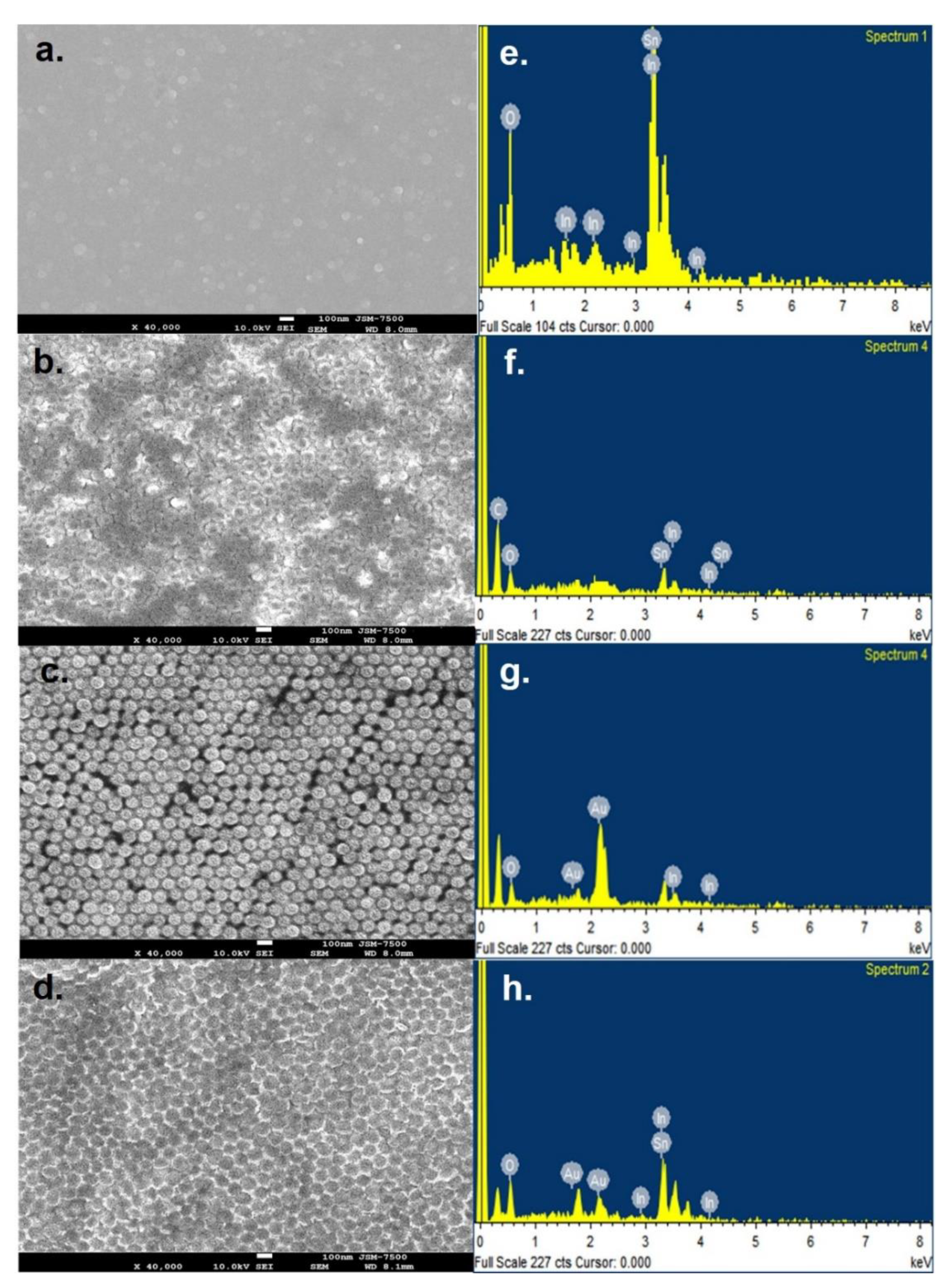
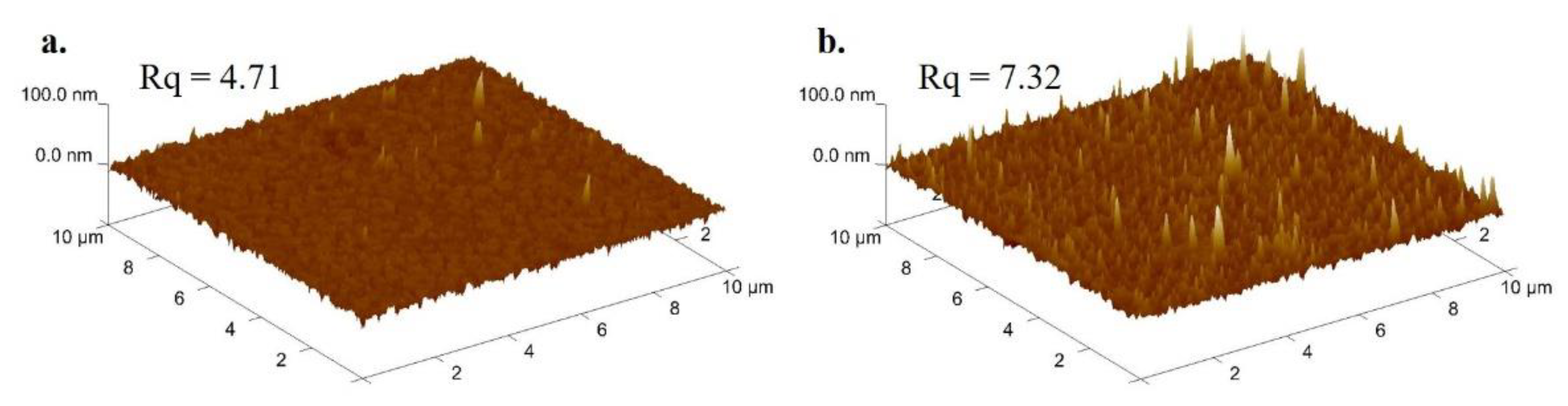
2.3.1. BGN and GNA Electrode Fabrication and Surface Characterization

The electrode surface nanostructure was templated using 100 nm diameter polystyrene nanobeads following our previously reported studies [26,28,39]. A 5 nm Au film was deposited onto the nanobead-covered ITO surface through a thermal evaporation process using a 2 nm Cr adhesion layer. The sensing area was defined in a circle area with d = 2 mm and mounted on a printed circuit board (PCB). The substrates were divided into two groups: one group proceeded with polystyrene nanobead etching with toluene, creating a periodic gold nanoframe array (GNA), and the other group was left without nanobead etching, generating a billowy gold nanostructure (BGN). The morphological characteristics of the substrates from each stage of modification were screened with AFM and FE-SEM with EDX analysis. The electroactive surface areas of the BGN and GNA electrodes were determined using cyclic voltammetry (CV) with potentials between −0.1 and 0.6 V, tested in a solution containing 5 × 10⁻⁶ mol/cm3 K3[Fe(CN)6] under a series of increasing scan rates.

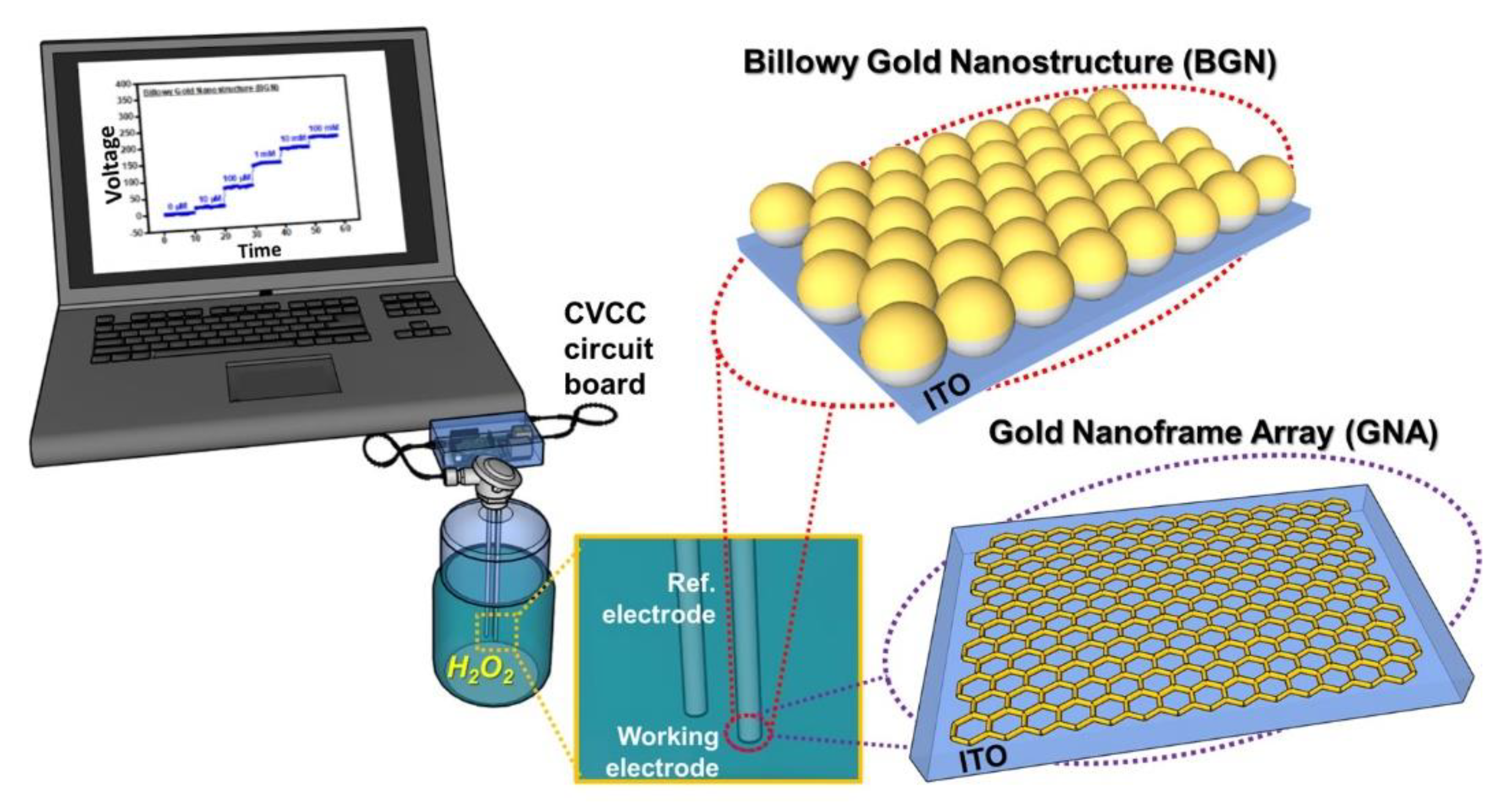
2.3.2. pH Measurement Using BGN and GNA Electrodes in the CVCC Circuit

To investigate the influence of the pH of the background buffer solution, the fabricated electrodes were immersed into a solution containing 50 mL of 10 mM H2O2 with various pH values ranging from pH 4 to pH 10, achieved by pH fixation with HCl and NaOH. The measurement was performed for 30 min for each pH value, and the last 10 output voltage points of the triplicate measurements using different sensing substrate produced under identical conditions, were extracted and plotted. The system was adjusted to measure 1 point per minute, and the measurement was performed with a fixed voltage across the gate and drain at 0.5 V, and a drain current at 100 µA.

2.3.3. H2O2 Detection using BGN and GNA Electrodes in the CVCC Circuit

The electrodes were immersed in a series of H2O2 concentrations prepared in 0.01× PBS (pH 7.4) as the background electrolyte with a total volume of 40 mL. The tested H2O2 aliquot ranged from 10 µM to 100 mM. The setup of the CVCC circuit used to record the output voltage versus time and the data point analysis is similar to the pH measurement mentioned above. The comprehensive experimental setup is presented in Figure 1.

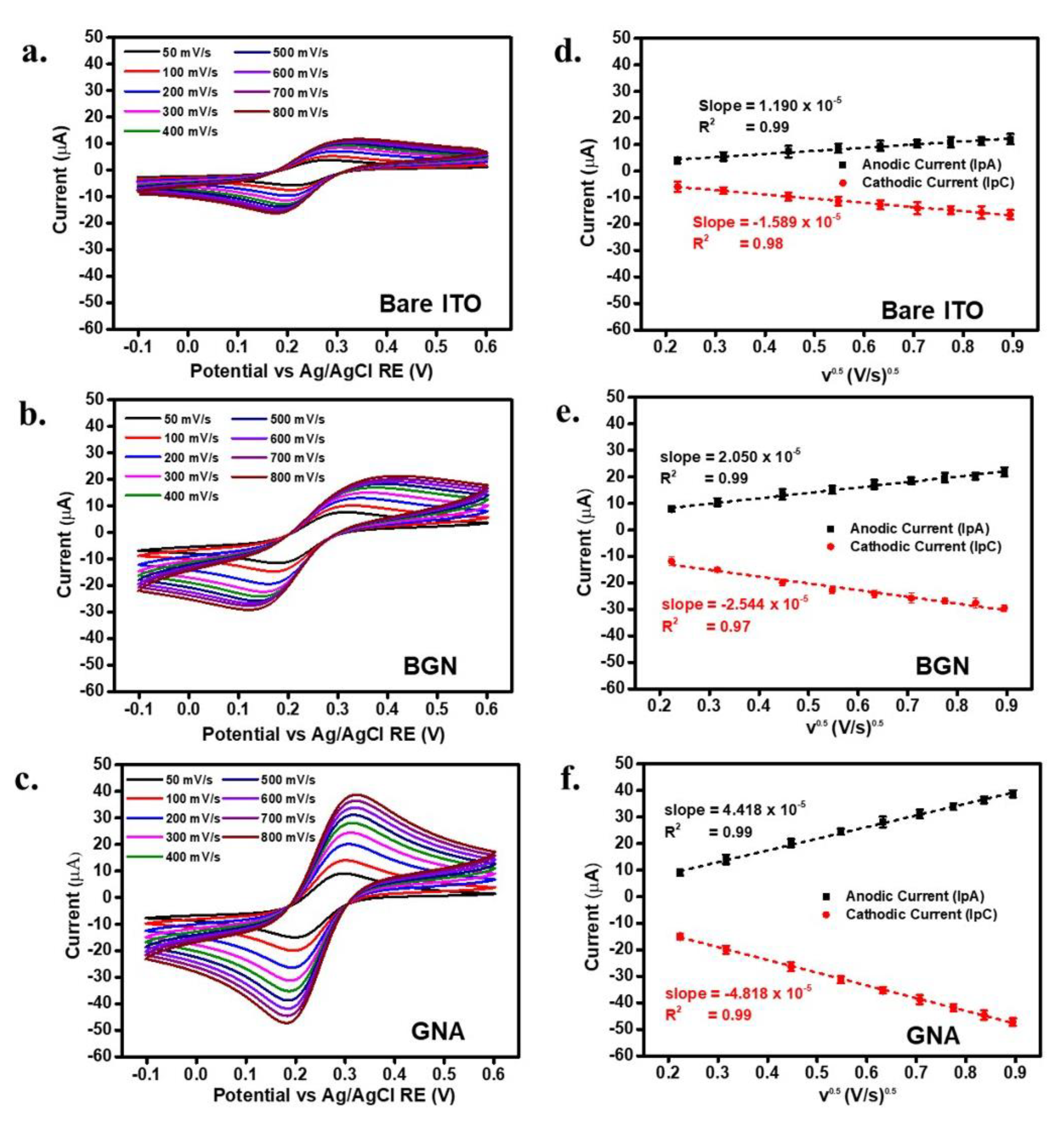
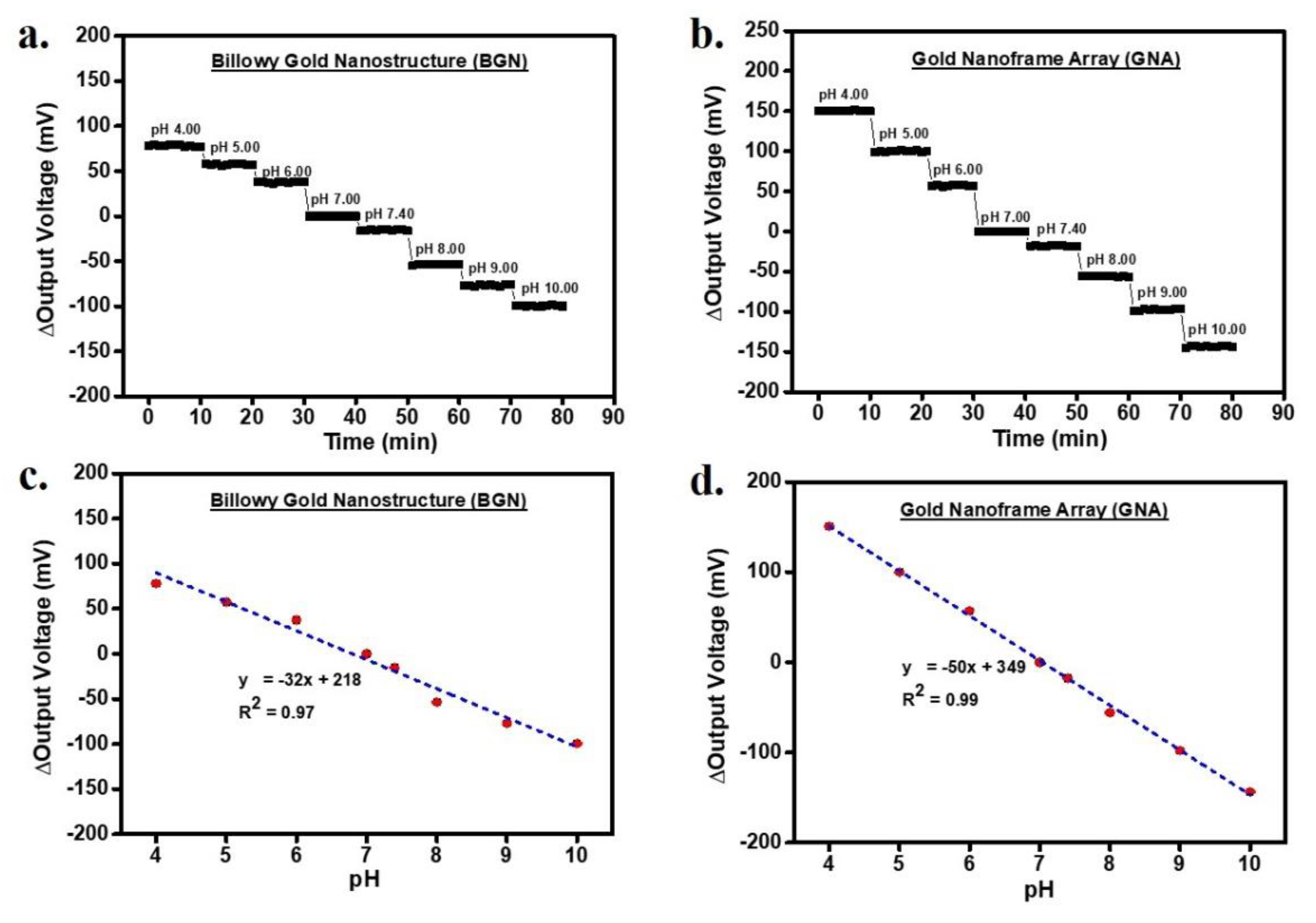
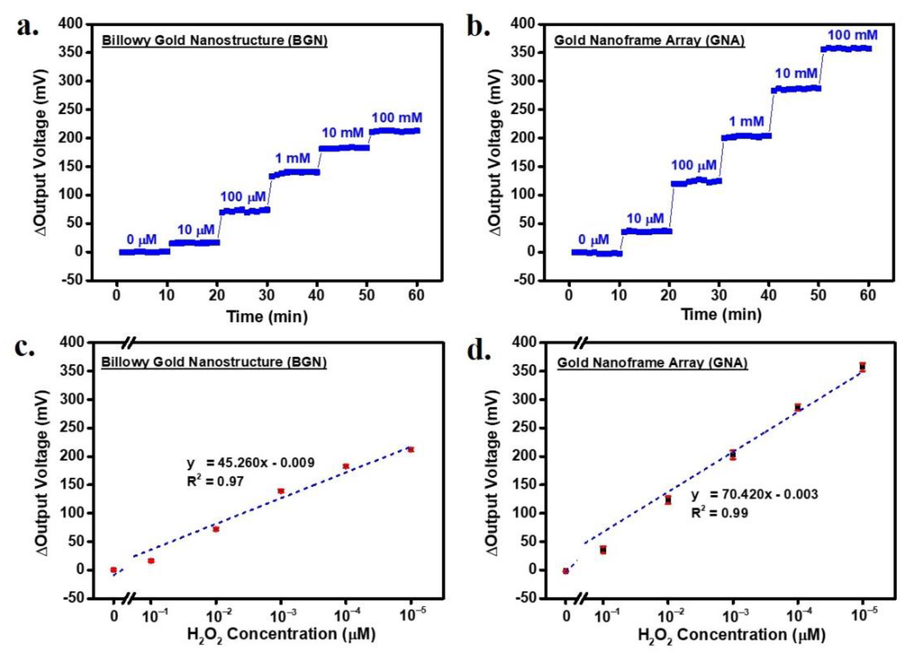
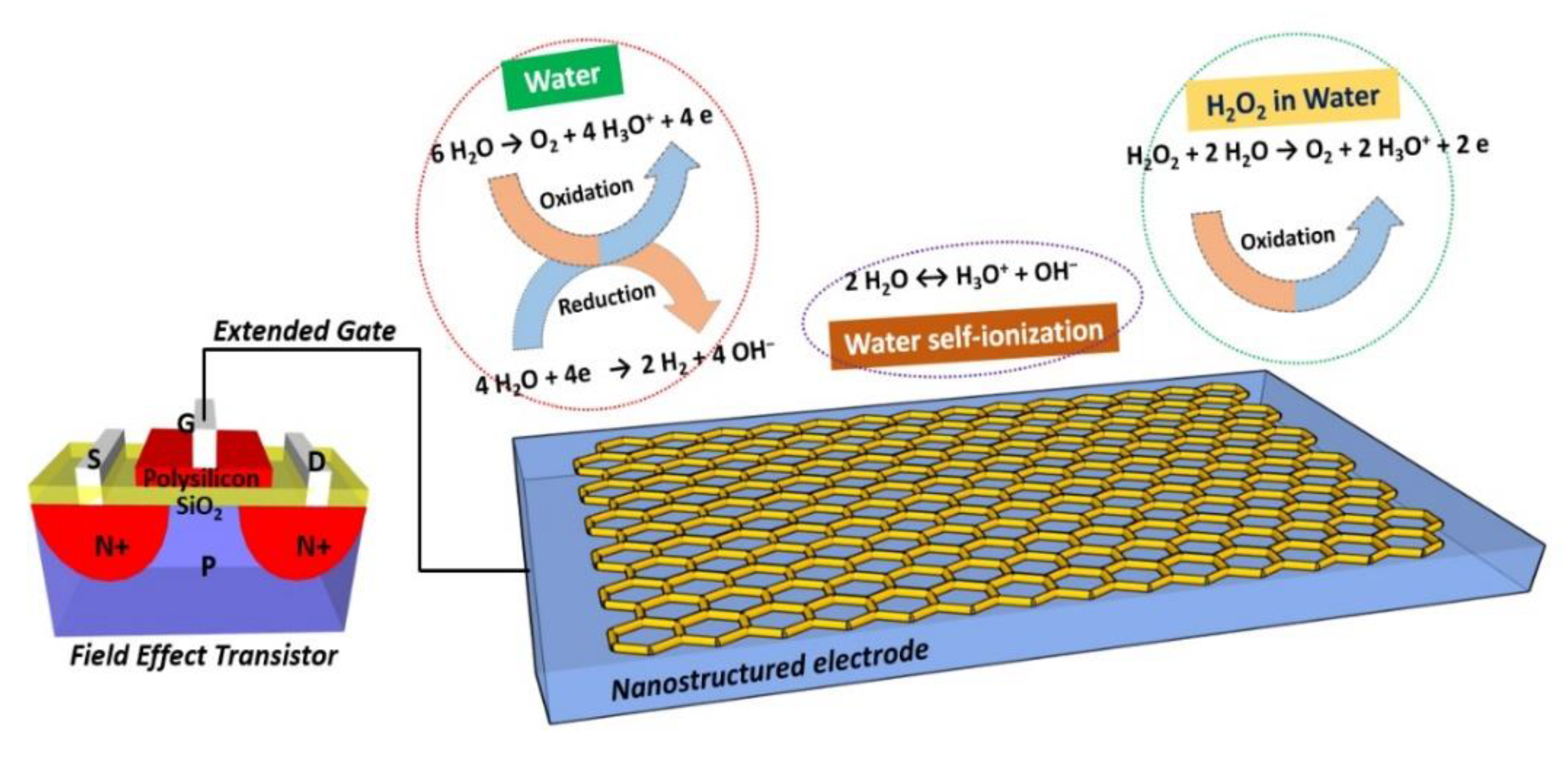
3. Results and Discussion

The deposition of monolayer polystyrene nanobeads onto the substrate is crucial in the initial stage of nanostructuring, while tiny particles with d < 200 nm exhibit a high tendency for forming clusters and multilayers [40]. The step-by-step surface nanostructuring is displayed in Figure 2. Starting from the bare ITO in Figure 2a, a cleaned ITO substrate was prepared before PS nanobead deposition. The transfer of the nanobeads results in a considerably monolayer coverage with minimum template dislocations on the hydrophilic ITO substrate as shown in Figure 2b. In working with small particles (d = ~100 nm), an equal portion of water facilitates faster ethanol evaporation. In addition, the surface tension is dominantly governed by the solid-to-liquid ratio (R) of the solid and liquid volume, creating a specific curvature of the liquid that should be maintained as positive [41]. In this work, we used an equal water-to-ethanol ratio of the nanobead mixture during the drop-casting method to facilitate obtaining the lowest energy configuration that leads to free diffusion of the particles across the substrate by providing a sufficient solvent amount to form a convex hull for monolayer deposition onto the substrate. Figure 2c showing the gold film-covered nanobeads on the ITO substrate concomitantly revalidates successful nanobead template transfer onto the ITO surface as well as the uniform Au film coverage onto it as observed in a higher resolution of SEM image than that of Figure 2b before Au film deposition. In most of the previously published works, NSL is incorporated in spin-coating, drop-casting, and dip-coating of larger nanobead templates with the reported typical defect-free (nanosphere polydispersity, site randomness, point defects (vacancies), line defects (slip dislocations), and polycrystalline domains) areas in the μm2 range [42]. With the approach of maintaining an equal solvent component ratio in the drop-casting method, we obtained a comparably high nanobead coverage area of ~6 µm2 with minimum site randomness and point defects (vacancies) using particle sizes as small as 100 nm. Nevertheless, as shown in Figure 2c, the billowy structure was evenly formed by the Au film due to the thermal evaporation process. It is observed that the gold film more predominantly covers the curvatures and the interstices between adjacent nanobeads rather than directly on the ITO, as seen by the brightness contrast in the few point defect sites. A contrast is seen in Figure 2d after nanobead template etching, which created a highly regular lattice of hexagonal Au nanoframes with a diameter of ~80 nm/frame in a considerably large surface area with only a minimum number of dislocated sites.
The surface nanostructuring stage is later validated with the EDX analysis. In the bare ITO substrate, the dominant elements of Sn, In, and O are observed in the EDX spectrum, as shown in Figure 2e. In contrast, after nanobead deposition onto ITO, the elemental percentage of ITO is noticed to be very low, while C, mainly composing the polymeric nanobead, is prominent as displayed in Figure 2f. The compositional analysis further shows that the Au particle percentage in BGN, as shown in Figure 2g, is nearly twice lower (with a value of 16.84%) than that in GNA, as shown in Figure 2h, which reaches the value of 30.64%. The honeycomb-like nanoframe array results from the highly regular and repetitive evaporation of gold in a considerably large area with a significant gold element percentage, indicating the suitability of the process for high-throughput fabrication. The overall NSL procedures only require less than 5 min to simultaneously deposit the monolayer PS nanobead onto two targeted ITO substrates. The reproducibility of the BGN and GNA electrodes’ morphology under different production batches is presented in FE-SEM graphs in Figure S1 (Supplementary Information).
The topological observation by AFM denotes that the BGN structure in Figure 3a exhibits a less spikey texture than the GNA structures that have noticeable protruding spicules, as shown in Figure 3b, mostly formed by the Au film that filled the void between the two nanobead templates after the etching process. This topography is linearly associated with the surface roughness properties, given by the Rq values of 4.71 nm for BGN and 7.32 nm for GNA. The higher surface roughness of GNA is significantly assisted by the etching of the templating particles and the strong adhesion of thermally evaporated gold, leaving firm regular ring-like arrays that are potentially beneficial for improved electron transport, ion penetration, and molecular entrapment.
In addition to determining the distinct Au array configuration and the Au particle percentage, surface roughness measurements were performed to validate the total usable nanostructured surface area for a larger sensing site as well as to overcome the challenge of ion interference during the measurement [43]. The two nanostructures were then subjected to cyclic voltammetry analysis using an ionic redox probe at a series of scan rates. In all the ITO, BGN, and GNA electrodes, as seen in Figure 4a–c, the peak current gradually increased with increasing scan rates. The increment of the current range (y-axis) is recorded with each stage of surface modification from bare ITO, BGN, and finally, GNA structures. This finding is correlated to the transformation of the surface morphology and topology in each surface modification, from bare ITO owning a planar 2D surface, BGN with its 3D curvy structure, and finally GNA with its larger surface area produced by its regular ring-like structure. The higher surface area in GNA allows a more intense redox reaction, which consequently requires higher currents in cyclic voltammetry. As shown in Figure 4d–f, the plot of the extracted anodic currents is linear with the square root of scan rates in the range 50–800 mV/s, reflecting the characteristics of a quasi-reversible diffusion-controlled electrode process [44]. The surface area calculation is performed using the Randles–Sevcik formula as follows [27,45]:
I p = ( 2.69 × 10 5 ) n 3 2 A D 0 1 2 C v 1 2
where I p is the peak current, n is the number of electrons transferred, A is the dimensional surface area, v is the scan rate, D 0 is the standard diffusion coefficient, equal to 7.6 × 10⁻⁶ cm2/s for K3Fe(CN)6, and C is the concentration of the K3Fe(CN)6 redox probe in the solution. Through this calculation, we observed a gradual increment of the electroactive surface area; 0.010, 0.017, and 0.037 cm2 for the bare ITO, BGN, and GNA electrodes, respectively. A comparison is made over the original geometric area, where the GNA dramatically increases the surface area by ~20%. The findings adequately support the morphological properties, as well as the surface roughness analysis via FE-SEM and AFM, and the GNA structure achieves optimized surface characteristics for ionic analyte sensing.
After surface characterization, the BGN and GNA electrodes were then tested in a portable CVCC circuit for the detection of pH to optimize the H2O2 measurement conditions. The CVCC circuit is explained in detail in [38]. The output voltage measurement with a series of pH values ranging from pH 4 to 10 in the background solution of 10 mM H2O2, as shown in Figure 5a,b, shows that the voltage rapidly decreased from pH 4 to 10 in BGN and GNA. The real-time measurement from the 10-min output voltage reading at each pH reveals that the CVCC circuit is highly stable, as indicated by the low standard deviations in both nanostructures. The Nernstian response of the pH sensitivity using the GNA electrode is higher, at ~50 mV/pH, as shown in Figure 5c, than that using the BGN electrode, which only reached ~32 mV/pH. Moreover, this result suggests that a neutral solution was the most optimized condition for the CVCC setup for H2O2 detection. Furthermore, by applying neutral pH as the background solution, we attempted to avoid the net balance charge (in the use of basis as the background solution) or the charge accumulation effects (in the use of acids as the background solution). It has been reported that the hollow structure in FET electrodes assists molecular and ionic transport at nanoscale dimensions and provides additional functional layers such as natural ionic membranes [46]. Moreover, wider diffusion of the H+ ions coupled to the floating gate applied by the CVCC circuit in this measurement setup could be obtained in GNA with its highly ordered cavities than in the BGN structure where a more concentrated ionic current occurs. In contrast, in GNA, the ionic current flows freely when the electrostatic potential across the Au ring array or volume exclusion and ion adsorption is altered [47].
The changes in output voltage were used to monitor the responses of the BGN and GNA electrodes upon the addition of H2O2 at various concentrations in real-time. The signal corresponding to H2O2 was extracted using the change in voltage (ΔVoutput = VH2O2 − VBlank), where VBlank is the output voltage from the measurement of 0.01× PBS without H2O2 and VH2O2 is the output voltage from the measurement of 0.01× PBS after the addition of a particular H2O2 concentration. Figure 6a,b presents the output voltage signal from both the BGN and GNA electrodes under different H2O2 concentrations in 0.01× PBS, exhibiting a trend of increased voltage with increasing H2O2 concentration in a fixed duration of the measurement, which may be ascribed to the presence of positive charges after H2O2 is introduced onto the interface [37], which will be explained in detail later. The results indicate that the GNA electrode has a higher output signal response range than the BGN electrode based on the detection of a series of H2O2 concentrations over a dynamic range of 10 µM to 100 mM, which may cover the H2O2 concentration range in both medical and environmental applications [33,34,35,48]. The sensitivity calculation derived from the linear fitting in the calibration plots in Figure 6c,d demonstrates that the GNA electrode presented a significantly higher sensitivity (~56%) than the BGN electrode. In the statistical analysis of H2O2 detection, all the standard deviations in the calibration plots were taken from triplicate measurements on an electrode fabricated and treated under similar conditions. The long-term stability of the sensors is tested in an hour measurement of 10 µM H2O2 in pH 7.40, as shown in Figure S2 (Supplementary Information). It is indicated that the GNA reaches faster stability than the BGN structures. Moreover, rigorous stability is also shown until the measurement completed in an hour. This supports the findings in the GNA’s higher electroactive surface area than the BGN, as well as the higher surface roughness facilitating more uniform ionic distribution at the interface. The limit of detection (LoD) was approximated from the minimum concentration of H2O2 solution that changed the output voltage signal under CVCC measurement, equivalent to three times the average background noise in the pure background solution (blank). In this study, the LoD calculation results in a lower value of 1.183 µM for GNA electrodes, while a higher LoD of 2.065 µM is obtained by the BGN electrode.
The findings in Figure 6 are supported by a schematic mechanism of H2O2 detection in neutral pH solution as shown in Figure 7. In our FET setup, the interfacial reaction comes from several phenomena [49]. First, it is initiated from the occurrence of water electrolysis events due to the electrical polarization at the surface as follows:
6 H2O → O2 + 4 H3O+ + 4 e (water oxidation)
4 H2O + 4 e → 2 H2 + 4 OH (water reduction)
Second, the self-ionization of water:
2 H2O ↔ H3O+ + OH
Third, when the H2O2 is introduced to the interface, the additional oxidation reaction occurs:
H2O2 + 2 H2O → O2 + 2 H3O+ + 2 e
From those reactions, the hydronium ions (H3O+) are highly produced and lead to the local pH drop. The positive charge accumulation results in the wider depletion layer on the FET channel because the Vref is a negative voltage. Subsequently, the current flow from drain (D) to source (S) drops. This state will be feedback information to increase the drain voltage to maintain the FET in the “on-state” condition and consequently triggers the increment of the output voltage.
A comparison of the proposed EGFET sensor system for H2O2 detection with other systems is listed in Table 1. In terms of sensing performance, there are some aspects to be improved compared to other methods. Nevertheless, the proposed measurement system in this research using the CVCC method leads to a fully portable design and low-power sensor platform. The circuit board power and data communication are connected by a universal serial bus (USB) cable from a laptop or by WiFi connection. Moreover, the signal acquisition software is user friendly, customized, and can be fully operated from a laptop.

4. Conclusions

This work presents a real-time, straightforward, miniaturized, and reliable sensing system for pH and H2O2 detection. Nanoscopic manipulation to create two distinct structures of ordered 2D gold arrays in subnanometer interstitial dimensions is achieved by NSL, enabling both bottom-up and top-down approaches of nanostructuring through a cost-effective and simple process with potential for high-throughput fabrication. The GNA, with its regular ring-like and spikey morphology produced by polystyrene nanobead template removal after gold film deposition, shows more prominent results in ionic screening by pH and H2O2 measurements due to its higher electroactive surface area than the BGN with periodic golden ball-like Au nanofilms covering the nonetched nanobead template. The integration of nanostructured electrodes with a portable multichannel CVCC circuit has realized a real-time and stable ion sensing system as an alternative to bulky conventional FET measurement systems and opens up the possibility for multiplex in situ detection in a remote and harsh screening environment. Further development would target the application of low-dimensional gate materials, such as graphene or carbon nanotubes (CNT) targeting the improvement of the LoD and sensitivity, as well as the realization of the wireless data acquisition and full integration to the smartphone app.

Supplementary Materials

The following are available online at https://0-www-mdpi-com.brum.beds.ac.uk/2227-9040/9/2/37/s1, Figure S1. The FE-SEM graphs showing the reproducibility of the fabricated electrodes with BGN structure from production in (a) Batch 1 and (b) Batch 2, in tilting position; and GNA structure from production in (c) Batch 1 (d) and Batch 2, captured in the same magnification. Figure S2. A one-hour measurement of using 10 µM H2O2 in pH 7.40 using BGN and GNA electrodes performed by a portable CVCC circuit.

Author Contributions

Conceptualization, A.P., Y.-C.T. and H.-L.L.; methodology, A.P. and G.M.A.S.; formal analysis, investigation, data curation, and validation, A.P., Y.-C.T., B.A.P. and G.M.A.S.; visualization, B.A.P.; writing—original draft preparation, original manuscript writing, A.P. and B.A.P.; writing—review and editing, A.P., Y.-C.T., B.A.P., C.-M.Y. and C.-S.L.; supervision, A.P., C.-M.Y. and C.-S.L. All authors have read and agreed to the published version of the manuscript.

Funding

This research was funded by Chang Gung Memorial Hospital, Taiwan under contract numbers CMRPD2K0051, CMRPD2K0171, CMRPD2I0012, and the Ministry of Science of Technology of Taiwan under contract numbers MOST:109-2221-E-182-013-MY3, 109-2622-8-182-001-TS1, 108-2221-E-182-060-MY3, 108-2628-E-182-002-MY3.

Institutional Review Board Statement

Not applicable.

Informed Consent Statement

Not applicable.

Data Availability Statement

The data presented in this study are available on request from the corresponding authors.

Acknowledgments

Gardin Muhammad Andika Saputra thanks Agnes Purwidyantri and Briliant Adhi Prabowo for the technical guidance during the science internship at the Indonesian Institute of Sciences (LIPI).

Conflicts of Interest

The authors declare no conflict of interest.

References

  1. Anastasios, V.; Adamos, C.; Libu, M.; Ravinder, D. Ultrathin Ion-Sensitive Field-Effect Transistor Chips with Bending-Induced Performance Enhancement. ACS Appl. Electron. Mater. 2020, 2, 2601–2610. [Google Scholar]
  2. Moreddu, R.; Elsherif, M.; Adams, H.; Moschou, D.; Cordeiro, M.F.; Wolffsohn, J.S.; Vigolo, D.; Butt, H.; Cooper, J.M.; Yetisen, A.K. Integration of paper microfluidic sensors into contact lenses for tear fluid analysis. Lab Chip 2020, 20, 3970–3979. [Google Scholar] [CrossRef] [PubMed]
  3. Gao, J.; Wang, Y.; Han, Y.; Gao, Y.; Wang, C.; Han, L.; Zhang, Y. Graphene-based field-effect transistors integrated with microfluidic chip for real-time pH monitoring of seawater. J. Mater. Sci. Mater. Electron. 2020, 31, 15372–15380. [Google Scholar] [CrossRef]
  4. Machado, R.C.L.; Alexis, F.; De Sousa, A.F.B.; Sousa, D. Nanostructured and Photochromic Material for Environmental Detection of Metal Ions. Molecules 2019, 24, 4243. [Google Scholar] [CrossRef] [PubMed] [Green Version]
  5. Wang, D.; Wang, Z.; Wang, X.; Zhuang, X.; Tian, C.; Luan, F.; Fu, X. Functionalized Copper Nanoclusters-Based Fluorescent Probe with Aggregation-Induced Emission Property for Selective Detection of Sulfide Ions in Food Additives. J. Agric. Food Chem. 2020, 68, 11301–11308. [Google Scholar] [CrossRef] [PubMed]
  6. Vivaldi, F.; SantaLucia, D.; Poma, N.; Bonini, A.; Salvo, P.; Del Noce, L.; Melai, B.; Kirchhain, A.; Kolivoška, V.; Sokolová, R.; et al. A voltammetric pH sensor for food and biological matrices. Sens. Actuators B Chem. 2020, 322, 128650. [Google Scholar] [CrossRef]
  7. Kaisti, M. Detection principles of biological and chemical FET sensors. Biosens. Bioelectron. 2017, 98, 437–448. [Google Scholar] [CrossRef]
  8. Pullano, S.A.; Critello, C.D.; Mahbub, I.; Tasneem, N.T.; Shamsir, S.; Islam, S.K.; Greco, M.; Fiorillo, A.S. EGFET-Based Sensors for Bioanalytical Applications: A Review. Sensors 2018, 18, 4042. [Google Scholar] [CrossRef] [Green Version]
  9. Liu, Y.-L.; Jin, Z.-H.; Hu, X.-B.; Qin, Y.; Xu, J.-Q.; Fan, C.-F.; Huang, W.-H. Stretchable Electrochemical Sensor for Real-Time Monitoring of Cells and Tissues. Angew. Chem. Int. Ed. 2016, 55, 4537–4541. [Google Scholar] [CrossRef] [PubMed]
  10. Melani, V.; Haddada, M.B.; Moustaoui, H.; Landoulsi, J.; Djaker, N.; Chapelle, M.L.; Spadavecchia, J. Pegylated doxorubicin gold complex: From nanovector to potential intercalant agent for biosensor applications. Front. Lab. Med. 2017, 1, 114–121. [Google Scholar] [CrossRef]
  11. Gupta, R.; Rai, B. Effect of Size and Surface Charge of Gold Nanoparticles on their Skin Permeability: A Molecular Dynamics Study. Sci. Rep. 2017, 7, 45292. [Google Scholar] [CrossRef] [Green Version]
  12. Bakshi, S.; Mehta, S.; Kumeria, T.; Shiddiky, M.J.A.; Popat, A.; Choudhury, S.; Bose, S.; Nayak, R. Rapid fabrication of homogeneously distributed hyper-branched gold nanostructured electrode based electrochemical immunosensor for detection of protein biomarkers. Sens. Actuators B Chem. 2021, 326, 128803. [Google Scholar] [CrossRef]
  13. Ma, H.; Chen, Z.; Gao, X.; Liu, W.; Zhu, H. 3D hierarchically gold-nanoparticle-decorated porous carbon for high-performance supercapacitors. Sci. Rep. 2019, 9, 1–10. [Google Scholar] [CrossRef] [PubMed]
  14. Song, H.Y.; Wong, T.I.; Sadovoy, A.; Wu, L.; Bai, P.; Deng, J.; Guo, S.; Wang, Y.; Knoll, W.; Zhou, X. Imprinted gold 2D nanoarray for highly sensitive and convenient PSA detection via plasmon excited quantum dots. Lab Chip 2015, 15, 253–263. [Google Scholar] [CrossRef] [PubMed]
  15. Fan, X.; Hao, Q.; Jin, R.; Huang, H.; Luo, Z.; Yang, X.; Chen, Y.; Han, X.; Sun, M.; Jing, Q.; et al. Assembly of gold nanoparticles into aluminum nanobowl array. Sci. Rep. 2017, 7, 1–7. [Google Scholar] [CrossRef] [PubMed]
  16. Wang, X.; Wang, Y.; Ye, X.; Wu, T.; Deng, H.; Wu, P.; Li, C. Sensing platform for neuron specific enolase based on molecularly imprinted polymerized ionic liquids in between gold nanoarrays. Biosens. Bioelectron. 2018, 99, 34–39. [Google Scholar] [CrossRef]
  17. Gao, Z.; Kang, H.; Naylor, C.H.; Streller, F.; Ducos, P.; Serrano, M.D.; Ping, J.; Zauberman, J.; Carpick, R.W.; Wang, Y.J.; et al. Scalable Production of Sensor Arrays Based on High-Mobility Hybrid Graphene Field Effect Transistors. ACS Appl. Mater. Interfaces 2016, 8, 27546–27552. [Google Scholar] [CrossRef]
  18. Tarasov, A.; Tsai, M.-Y.; Flynn, E.M.; Joiner, C.A.; Taylor, R.C.; Vogel, E.M. Gold-coated graphene field-effect transistors for quantitative analysis of protein–antibody interactions. 2D Mater. 2015, 2, 044008. [Google Scholar] [CrossRef] [Green Version]
  19. Ban, T.; Uenuma, M.; Migita, S.; Okamoto, N.; Ishikawa, Y.; Uraoka, Y.; Yamashita, I.; Yamamoto, S.-I. One-dimensional array of gold nanoparticles fabricated using biotemplate and its application to fine FET. Jpn. J. Appl. Phys. 2018, 57, 06HC05. [Google Scholar] [CrossRef] [Green Version]
  20. Paik, S.; Kim, G.; Chang, S.; Lee, S.; Jin, D.; Jeong, K.-Y.; Lee, I.S.; Lee, J.; Moon, H.; Lee, J.; et al. Near-field sub-diffraction photolithography with an elastomeric photomask. Nat. Commun. 2020, 11, 805. [Google Scholar] [CrossRef] [Green Version]
  21. Acikgoz, C.; Hempenius, M.A.; Huskens, J.; Vancso, G.J. Polymers in conventional and alternative lithography for the fabrication of nanostructures. Eur. Polym. J. 2011, 47, 2033–2052. [Google Scholar] [CrossRef] [Green Version]
  22. Qin, D.; Xia, Y.; Whitesides, G.M. Soft lithography for micro- and nanoscale patterning. Nat. Protoc. 2010, 5, 491–502. [Google Scholar] [CrossRef] [Green Version]
  23. Xu, X.; Yang, Q.; Wattanatorn, N.; Zhao, C.; Chiang, N.; Jonas, S.J.; Weiss, P.S. Multiple-Patterning Nanosphere Lithography for Fabricating Periodic Three-Dimensional Hierarchical Nanostructures. ACS Nano 2017, 11, 10384–10391. [Google Scholar] [CrossRef] [PubMed]
  24. Wahle, M.; Brassat, K.; Ebel, J.; Bürger, J.; Lindner, J.K.N.; Kitzerow, H.-S. Two-dimensional switchable blue phase gratings manufactured by nanosphere lithography. Opt. Express 2017, 25, 22608. [Google Scholar] [CrossRef] [PubMed]
  25. Lin, B.-C.; Ku, C.-S.; Lee, H.-Y.; Wu, A.T. Epitaxial growth of ZnO nanorod arrays via a self-assembled microspheres lithography. Appl. Surf. Sci. 2017, 414, 212–217. [Google Scholar] [CrossRef]
  26. Purwidyantri, A.; Hsu, C.-H.; Yang, C.-M.; Prabowo, B.A.; Tian, Y.-C.; Lai, C.-S. Plasmonic nanomaterial structuring for SERS enhancement. RSC Adv. 2019, 9, 4982–4992. [Google Scholar] [CrossRef] [Green Version]
  27. Purwidyantri, A.; Chen, C.-H.; Hwang, B.-J.; Luo, J.-D.; Chiou, C.-C.; Tian, Y.-C.; Lin, C.-Y.; Cheng, C.-H.; Lai, C.-S. Spin-coated Au-nanohole arrays engineered by nanosphere lithography for a Staphylococcus aureus 16S rRNA electrochemical sensor. Biosens. Bioelectron. 2016, 77, 1086–1094. [Google Scholar] [CrossRef] [PubMed]
  28. Purwidyantri, A.; Kamajaya, L.; Chen, C.-H.; Luo, J.-D.; Chiou, C.-C.; Tian, Y.-C.; Lin, C.-Y.; Yang, C.-M.; Lai, C.-S. A Colloidal Nanopatterning and Downscaling of a Highly Periodic Au Nanoporous EGFET Biosensor. J. Electrochem. Soc. 2018, 165, H3170–H3177. [Google Scholar] [CrossRef]
  29. Ivanova, A.S.; Merkuleva, A.D.; Andreev, S.V.; Sakharov, K.A. Method for determination of hydrogen peroxide in adulterated milk using high performance liquid chromatography. Food Chem. 2019, 283, 431–436. [Google Scholar] [CrossRef]
  30. Liu, T.; Clegg, S.L.; Abbatt, J.P.D. Fast oxidation of sulfur dioxide by hydrogen peroxide in deliquesced aerosol particles. Proc. Natl. Acad. Sci. USA 2020, 117, 1354–1359. [Google Scholar] [CrossRef]
  31. Liu, Y.; Bai, L.; Li, Y.; Ni, Y.; Xin, C.; Zhang, C.; Liu, J.; Liu, Z.; Li, L.; Huang, W. Visualizing hydrogen peroxide in Parkinson’s disease models via a ratiometric NIR fluorogenic probe. Sens. Actuators B Chem. 2019, 279, 38–43. [Google Scholar] [CrossRef]
  32. Yang, J.; Yang, J.; Liang, S.H.; Xu, Y.; Moore, A.; Ran, C. Imaging hydrogen peroxide in Alzheimer’s disease via cascade signal amplification. Sci. Rep. 2016, 6, 35613. [Google Scholar] [CrossRef] [PubMed] [Green Version]
  33. Huang, B.K.; Sikes, H.D. Quantifying intracellular hydrogen peroxide perturbations in terms of concentration. Redox Biol. 2014, 2, 955–962. [Google Scholar] [CrossRef] [Green Version]
  34. Di Marzo, N.; Chisci, E.; Giovannoni, R. The Role of Hydrogen Peroxide in Redox-Dependent Signaling: Homeostatic and Pathological Responses in Mammalian Cells. Cells 2018, 7, 156. [Google Scholar] [CrossRef] [Green Version]
  35. Jacewicz, D.; Siedlecka-Kroplewska, K.; Drzeżdżon, J.; Piotrowska, A.; Wyrzykowski, D.; Tesmar, A.; Żamojć, K.; Chmurzyński, L. Method for detection of hydrogen peroxide in HT22 cells. Sci. Rep. 2017, 7, srep45673. [Google Scholar] [CrossRef] [Green Version]
  36. Al-Hardan, N.H.; Abdul Hamid, M.A.; Shamsudin, R.; Al-Khalqi, E.M.; Kar Keng, L.; Ahmed, N.M. Electrochemical hy-drogen peroxide sensor based on macroporous silicon. Sensors 2018, 18, 716. [Google Scholar] [CrossRef] [PubMed] [Green Version]
  37. Zheng, C.; Jin, X.; Li, Y.; Mei, J.; Sun, Y.; Xiao, M.; Zhang, H.; Zhang, Z.; Zhang, G.-J. Sensitive Molybdenum Disulfide Based Field Effect Transistor Sensor for Real-time Monitoring of Hydrogen Peroxide. Sci. Rep. 2019, 9, 759. [Google Scholar] [CrossRef]
  38. Chung, W.-Y.; Lin, Y.-T.; Pijanowska, D.G.; Yang, C.-H.; Wang, M.-C.; Krzyskow, A.; Torbicz, W. New ISFET interface circuit design with temperature compensation. Microelectron. J. 2006, 37, 1105–1114. [Google Scholar] [CrossRef]
  39. Purwidyantri, A.; El-Mekki, I.; Lai, C.-S. Tunable Plasmonic SERS “Hotspots” on Au-Film over Nanosphere by Rapid Thermal Annealing. IEEE Trans. Nanotechnol. 2017, 16, 551–559. [Google Scholar] [CrossRef]
  40. Chau, C.F.; Melvin, T. The fabrication of macroporous polysilicon by nanosphere lithography. J. Micromech. Microeng. 2008, 18, 064012. [Google Scholar] [CrossRef]
  41. Chandramohan, A.; Sibirev, N.V.; Dubrovskii, V.G.; Petty, M.C.; Gallant, A.J.; Zeze, D.A. Model for large-area monolayer coverage of polystyrene nanospheres by spin coating. Sci. Rep. 2017, 7, 40888. [Google Scholar] [CrossRef] [Green Version]
  42. Haynes, C.L.; Van Duyne, R.P. Nanosphere Lithography: A Versatile Nanofabrication Tool for Studies of Size-Dependent Nanoparticle Optics. J. Phys. Chem. B 2001, 105, 5599–5611. [Google Scholar] [CrossRef]
  43. Fakih, I.; Durnan, O.; Mahvash, F.; Napal, I.; Centeno, A.; Zurutuza, A.; Yargeau, V.; Szkopek, T. Selective ion sensing with high resolution large area graphene field effect transistor arrays. Nat. Commun. 2020, 11, 1–12. [Google Scholar] [CrossRef] [PubMed]
  44. Fu, K.; Bohn, P.W. Nanopore Electrochemistry: A Nexus for Molecular Control of Electron Transfer Reactions. ACS Cent. Sci. 2017, 4, 20–29. [Google Scholar] [CrossRef] [PubMed] [Green Version]
  45. Ferrari, A.G.-M.; Foster, C.W.; Kelly, P.J.; Brownson, D.A.C.; Banks, C.E. Determination of the Electrochemical Area of Screen-Printed Electrochemical Sensing Platforms. Biosensors 2018, 8, 53. [Google Scholar] [CrossRef] [Green Version]
  46. Shim, J.H.; Kim, J.; Cha, G.S.; Nam, H.; White, R.J.; White, H.S.; Brown, R.B. Glass nanopore-based ion-selective electrodes. Anal. Chem. 2007, 79, 3568–3574. [Google Scholar] [CrossRef] [PubMed]
  47. Kasianowicz, J.J.; Balijepalli, A.K.; Ettedgui, J.; Forstater, J.H.; Wang, H.; Zhang, H.; Robertson, J.W. Analytical applications for pore-forming proteins. Biochim. Biophys. Acta Biomembr. 2016, 1858, 593–606. [Google Scholar] [CrossRef]
  48. Anh, D.T.; Olthuis, W.; Bergveld, P. A hydrogen peroxide sensor for exhaled breath measurement. Sens. Actuators B Chem. 2005. [Google Scholar] [CrossRef] [Green Version]
  49. Diallo, A.K.; Djeghlaf, L.; Launay, J.; Temple-Boyer, P. Modelling of Impulsional pH Variations Using ChemFET-Based Microdevices: Application to Hydrogen Peroxide Detection. Sensors 2014, 14, 3267–3283. [Google Scholar] [CrossRef] [Green Version]
  50. Anh, D.T.; Olthuis, W.; Bergveld, P. Hydrogen peroxide detection with improved selectivity and sensitivity using constant current potentiometry. Sens. Actuators B Chem. 2003, 91, 1–4. [Google Scholar] [CrossRef]
  51. Kotchey, G.P.; Allen, B.L.; Vedala, H.; Yanamala, N.; Kapralov, A.A.; Tyurina, Y.Y.; Klein-Seetharaman, J.; Kagan, V.E.; Star, A. The Enzymatic Oxidation of Graphene Oxide. ACS Nano 2011, 5, 2098–2108. [Google Scholar] [CrossRef] [PubMed]
  52. Park, J.W.; Park, S.J.; Kwon, O.S.; Lee, C.; Jang, J. Polypyrrole Nanotube Embedded Reduced Graphene Oxide Transducer for Field-Effect Transistor-Type H2O2 Biosensor. Anal. Chem. 2014, 86, 1822–1828. [Google Scholar] [CrossRef] [PubMed]
  53. Kim, W.; Shin, D.H.; Jun, J.; Kim, J.H.; Jang, J. Fabrication of Shape-Controlled Palladium Nanoparticle-Decorated Elec-trospun Polypyrrole/Polyacrylonitrile Nanofibers for Hydrogen Peroxide Coalescing Detection. Adv. Mater. Interfaces 2017, 4, 1700573. [Google Scholar] [CrossRef]
  54. Lee, S.H.; Kim, K.H.; Seo, S.E.; Kim, M.I.; Park, S.J.; Kwon, O.S. Cytochrome C-decorated graphene field-effect transistor for highly sensitive hydrogen peroxide detection. J. Ind. Eng. Chem. 2020, 83, 29–34. [Google Scholar] [CrossRef]
Figure 1. Schematic diagram of the real-time H2O2 sensing setup using a billowy gold nanostructure (BGN) and gold nanoframe array (GNA) extended-gate field-effect transistor (EGFET) integrated with a portable constant voltage–constant current (CVCC) circuit system.
Chemosensors 09 00037 g001
Figure 2. Field emission-scanning electron microscopy (FE-SEM) micrographs of (a) bare ITO, (b) polystyrene (PS) nanobead-covered ITO, (c) billowy gold nanostructure (BGN), (d) gold nanoframe array (GNA), and energy-dispersive X-ray spectroscopy (EDX) spectra of (e) bare ITO, (f) PS nanobead-covered ITO, (g) BGN, and (h) GNA.
Chemosensors 09 00037 g002
Figure 3. Atomic force microscopy (AFM) surface roughness profiling of (a) billowy gold nanostructure (BGN) and (b) gold nanoframe array (GNA) structures.
Chemosensors 09 00037 g003
Figure 4. Cyclic voltammograms and the linear relations of the anodic peak current against the scan rate’s square root of the (a,d) bare ITO, (b,e) billowy gold nanostructure (BGN), and (c,f) gold nanoframe array (GNA) electrodes.
Chemosensors 09 00037 g004
Figure 5. Real-time measurement of pH in 10 mM H2O2 and the respective calibration plots performed by a portable CVCC circuit using the (a,c). billowy gold nanostructure (BGN) and (b,d). gold nanoframe array (GNA) electrodes.
Chemosensors 09 00037 g005
Figure 6. Real-time measurement of H2O2 solution and the respective calibration plots performed by a portable CVCC circuit using the (a,c). billowy gold nanostructure (BGN) and (b,d). gold nanoframe array (GNA) electrodes.
Chemosensors 09 00037 g006
Figure 7. The water-based ion generation during H2O2 detection.
Chemosensors 09 00037 g007
Table 1. Comparison of FET-based H2O2 sensors in terms of sensing structure, measurement technique, portability, and performance.
FET Sensor StructureMeasurement TechniquePortabilityQuantification PerformanceRef
Remote Pt gate electrode (electroactive gate MOSFET)Vth measurementNoTunable sensitivity: 221–720 mV/decade[50]
rGO FET with a back gateVth measurementNo∼40 μM[51]
Electrochemical Field-Effect Transistor (ElecFET)Vth measurementNoMeasurement range: 1–150 mM[49]
Polypyrrole Nanotube Embedded rGO FETIDS measurementNoLoD: 100 pM[52]
Pd Nanoparticle at Polypyrrole/Polyacrylonitrile NanofibersIDS measurementNoLoD: 1 nM[53]
MOS2/rGO FETIDS measurementNoLoD: 1 pM[37]
Cytochrome c modified single-layered graphene FETIDS measurementNoLoD: 100 fM[54]
Gold nanoframe array on EGFETVs on CVCC systemYesSensitivity: 70 mV/decade
LoD: 1.183 µM
This work
Publisher’s Note: MDPI stays neutral with regard to jurisdictional claims in published maps and institutional affiliations.

