
Metal–Oxide Nanowire Molecular Sensors and Their Promises
by
 , ,
, ,
Hao Zeng
1 ,
,
Guozhu Zhang
1,*, 
Kazuki Nagashima
1,2,
Tsunaki Takahashi
1,2,
Takuro Hosomi
1,2 and
Takeshi Yanagida
1,3,* 1
Department of Applied Chemistry, Graduate School of Engineering, The University of Tokyo, 7-3-1, Hongo, Bunkyo-ku, Tokyo 113-8654, Japan
2
JST-PRESTO, 4-1-8 Honcho, Kawaguchi, Saitama 332-0012, Japan
3
Institute for Materials Chemistry and Engineering, Kyushu University, 6-1 Kasuga-Koen, Kasuga, Fukuoka 816-8580, Japan
*
Authors to whom correspondence should be addressed.
Chemosensors 2021, 9(2), 41; https://0-doi-org.brum.beds.ac.uk/10.3390/chemosensors9020041
Submission received: 15 January 2021
/
Revised: 15 February 2021
/
Accepted: 19 February 2021
/
Published: 22 February 2021
(This article belongs to the Special Issue Nanomaterials-Based Sensors)
Abstract
:During the past two decades, one–dimensional (1D) metal–oxide nanowire (NW)-based molecular sensors have been witnessed as promising candidates to electrically detect volatile organic compounds (VOCs) due to their high surface to volume ratio, single crystallinity, and well-defined crystal orientations. Furthermore, these unique physical/chemical features allow the integrated sensor electronics to work with a long-term stability, ultra-low power consumption, and miniature device size, which promote the fast development of “trillion sensor electronics” for Internet of things (IoT) applications. This review gives a comprehensive overview of the recent studies and achievements in 1D metal–oxide nanowire synthesis, sensor device fabrication, sensing material functionalization, and sensing mechanisms. In addition, some critical issues that impede the practical application of the 1D metal–oxide nanowire-based sensor electronics, including selectivity, long-term stability, and low power consumption, will be highlighted. Finally, we give a prospective account of the remaining issues toward the laboratory-to-market transformation of the 1D nanostructure-based sensor electronics.
1. Introduction
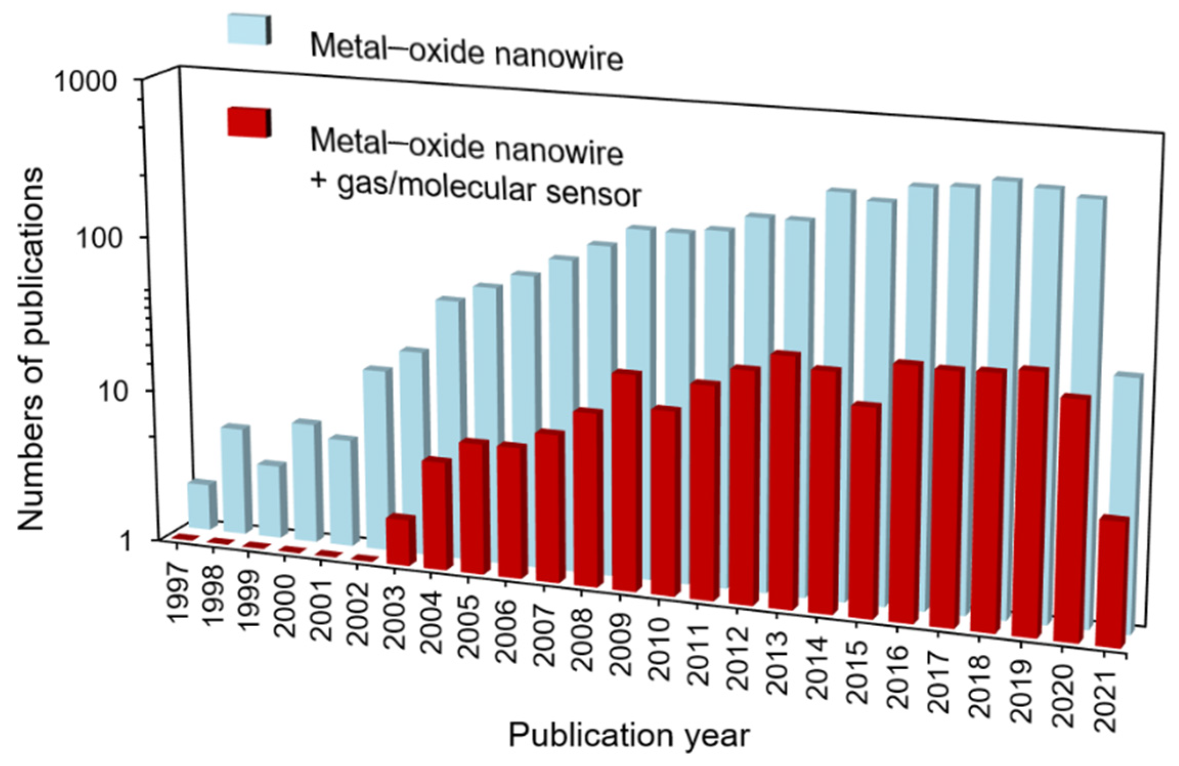
For the upcoming “trillion sensor electronics” era, molecular sensor and electronic recognition devices, which collect the enormous chemical information as big data from various volatile organic molecules (VOCs), are gaining increasing interests in health care [1,2,3], environment [1,4,5], security [6,7,8,9] and agriculture areas [3,4,10,11]. Among various molecular sensors, chemiresistive sensors integrated with metal–oxide semiconductor (MOS) nanostructures are of particular interest due to their high sensitivity and fast response [12,13,14,15,16]. Especially with the advancement of nanomaterial fabrication technology, a large number of functional MOS nanostructures, such as nanodots [17,18], nanowires [19,20,21,22], nanosheets [23,24,25], and hierarchical nanostructures [26,27,28], are synthesized as building blocks for the fabrication of sensor electronics.
Among these nanostructured forms, 1D MOS nanowires offer an ideal platform for nanoscale sensor integration due to their high surface to volume ratio, comparable sized Debye length, high crystallinity, excellent surface chemical reaction, and low power consumption [29,30,31]. Ever since the first report of using the 1D metal–oxide nanostructure as the gas sensor by Comini, great progress has been achieved in the past two decades [32]. To date, hundreds of papers have been published on molecular sensors integration based on 1D metal–oxide nanostructures (SnO2 [29], In2O3 [33], Fe2O3 [34], V2O5 [35], CeO2 [36], ZnO [37], WO3 [38], NiO [39], CuO [40], NaNbO3 [41], Zn2SnO4 [42,43], CdIn2O4 [44], etc.), and the numbers of publications related to nanowires and metal–oxide nanowire sensors can be seen in Figure 1. Meanwhile, to fulfill multiple demands of molecule detection and monitoring, nanowire-based sensor devices with different structures, such as flat [45], suspended [46], bridging [47], and vertical structure [48], have also been addressed. Despite much effort being devoted to advancing the metal–oxide nanowire-based molecular sensor electronics, molecular sensors based on 1D MOS nanowires have not yet been successfully commercialized compared to the MOS film structures.
The inherent limitations for the practical applications of the 1D MOS nanowire-based molecular sensors can be summarized as follows:
(1) Lack of effective method for the large-scale synthesis of geometrically uniform single-crystalline nanowires—as is known, the electrical [49], optical [50], thermal [51], and chemical [52] properties of nanomaterials are strongly affected by their size and shape due to the quantum confinement effect [53]. The electrical conduction becomes more sensitive to the field-effect as the nanowire diameter decreases [54]. Until now, although highly crystalline MOS nanowire with various diameters [55], compositions [28,29,30,31,32,33,34,35,36,37,38,39,40] and heterostructures [56,57] can be grown in vapor phase (physical vapor deposition (PVD) [58,59], pulsed laser ablation deposition (PLD) [60,61] and chemical vapor deposition (CVD) [62,63], etc.) and solution phase (hydrothermal [64,65] and solvothermal [66,67]), the large-scale synthesis of geometry uniform (diameter) nanowires is still a big challenge [68].
(2) Poor reproducibility—it has been demonstrated that the nanowires present a fantastic performance as they are integrated into single nanowire devices [69]. For such a kind of device, lithography and sputtering techniques are frequently utilized to design and deposit interdigitated electrodes on randomly distributed nanowires for the device fabrication [70]. However, this process is only accessible for fundamental laboratory research, and assembling scalable and controllable nanowires on arbitrary substrates remain a major challenge toward performance reproducible sensor device fabrication [71].
(3) Poor environmental/thermal stability—to deeply exploit the data science from the obtained sensor signal, the long-term stability of the sensor response is highly required for time-series data collection [72]. However, performance degradation usually occurs in the nanowire-based sensor electronics because the surrounding oxygen, water, and contaminates would react with the active nanowire surface as well as the nanowire–electrode contact when the sensors are exposed to ambient air for molecular detection [47,73,74].
(4) Poor sensor selectivity—although the sensitivity of the single nanowire sensor devices has been demonstrated to possess an exponential enhancement as compared with those thin-film devices [75,76], it is still desired to significantly improve the selectivity of nanowire-based sensor electronics. Therefore, further efforts are still encouraged to promote MOS nanowire-based sensor electronics for the IoT applications.
Here, in this review, we first give a comprehensive overview of the recent studies and achievements in 1D MOS nanowire synthesis, sensor device fabrication, device functionalization, and sensing mechanisms. Then, some critical issues that impede the practical application of the 1D MOS nanowire-based sensor electronics, including selectivity, long-term stability, and low power consumption, will be pointed out. Finally, we give an outlook of the remaining issues towards the lab-to-market transfer of the 1D nanostructure-based sensor electronics.
2. Metal–oxide Nanowires Growth
Nanowire-based electronics offers an excellent possibility for future systems beyond the limitation of Moore’s law and provides a promising platform to explore the physical origin and intrinsic properties. In recent decades, significant efforts and progress have been made, and many methods have been developed to synthesize 1D metal–oxide nanowires, including PVD, CVD, PLD, thermal oxidization and solution-based growth for single-crystalline nanowires, and template growth, electro-spun for polycrystalline/amorphous nanowires. Here, this section will mainly focus on the metal–oxide nanowires growth mechanism.
2.1. Vapor–Liquid–Solid Growth (VLS Growth)
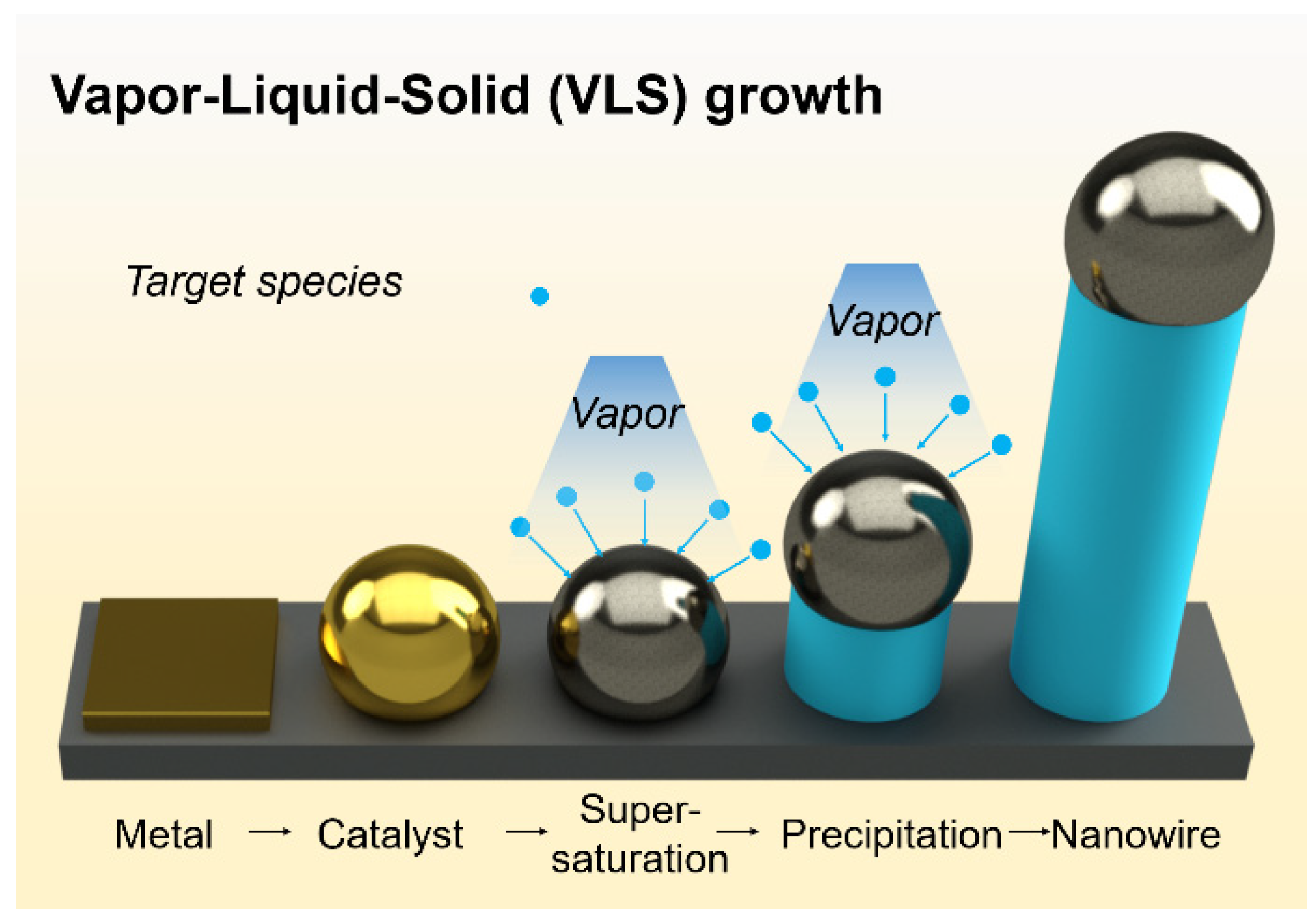
The vapor–liquid–solid (VLS) mechanism is widely employed to grow high-quality nanowires [77,78,79,80,81,82,83,84,85,86,87,88,89]. In a typical VLS growth, as shown in Figure 2, a metallic catalyst droplet is firstly formed via heating the pre-deposited metal catalyst thin film. Then, by continuously feeding the vapor species to the metallic catalyst at an elevated temperature, a liquid eutectic alloy is formed. Finally, once the alloy reaches super-saturation, nanowires can be anisotropically grown from the nucleated seeds at the liquid–solid interface and the length of nanowires can be controlled by the growth time.
In 1998, the Lieber group firstly reported a laser ablation technique for gaining VLS silicon nanowires [81]. Following this interesting work, various methods such as CVD, PVD, PLD, electron beam evaporation, and molecular beam epitaxy (MBE) have been developed to grow the metal–oxide nanowires ITO [90,91,92], NiO [93,94,95], ZnO [83,96], SnO2 [97,98], TiO2 [99,100], In2O3 [101,102], MgO [103,104,105], etc. [106,107].
In recent years, the Yanagida Lab (The University of Tokyo) has made great efforts in the VLS growth of metal–oxide nanowires [85,86,94,98,99,105,108,109,110,111,112,113,114,115,116,117,118,119,120,121,122,123,124,125,126,127,128,129,130,131]. They have pointed out that materials flux is an important variable which has been underestimated in VLS nanowires growth. For example, via precisely controlling the material flux within an order of magnitude, the structure and composition of VLS growth ITO nanowires can be altered from Rutile structure (Sn 100%, In 0%) to Fluorite structure (Sn 28%, In 72%) and Bixbyite structure (Sn 21%, In 79%) [86]. Moreover, the proposed “material flux window” concept from their group has been successfully applied for the synthesis of SnO2, In2O3, ITO, ZnO, NiO, MnO, CaO, Sm2O3, Eu2O3 and MgO nanowires [85]. Nevertheless, the VLS process of metal–oxides growth generally requires relatively high temperatures (600–1000 °C), which essentially limits their practical applications.
To solve this problem, Zhu et al. demonstrated a rational method to reduce the growth temperature via using the concept of “materials flux window” [83]. As shown in Figure 3a, it was found that a reduction in growth temperature can be successfully achieved via precisely controlling the vapor flux which originates from the suppression of nucleation at the vapor–solid interface. By optimizing an appropriate vapor flux for VLS nanowire, this concept can be applied to reduce the growth temperature for various metal–oxides, including ZnO (from 750 to 400 °C), SnO2 (from 750 to 400 °C), and MgO (from 800 to 350 °C), as shown in Figure 3b–d. In addition, it has shown a successful application of this concept for the VLS growth SnO2 nanowire on tin-doped indium oxide (ITO) glass at 500 °C and ZnO nanowires on polyimide (PI) substrates at 350 °C.
2.2. Vapor–Solid Growth (VS Growth)
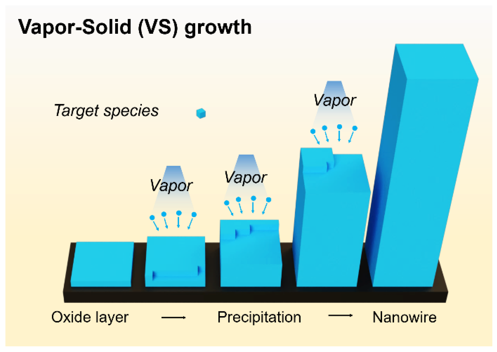
In the absence of a metal catalyst, 1D material structures can also be directly formed from the vapor phase into the solid phase, that is, the VS growth (Figure 4). In the view of the current studies, VS growth mechanisms are generally concluded as three types: (1) The anisotropic growth mechanism: nanowires can be synthesized via the preferential reactivity and binding of gas reactants on a specific surface to minimize the total surface energy [132,133,134]; (2) The defect-induced growth (or screw dislocations) mechanism: the growth of crystal proceeds by adding atoms at the kink sites of a surface step [135,136,137,138,139]; (3) The self-catalytic growth mechanism: metal–oxide can be decomposed into metal and oxygen by heating under vacuum condition, then the metal vapors are condensed and forming liquid droplets on a lower temperature substrate, and such droplets are the ideal catalysts for metal–oxide nanowire growth [140,141,142,143,144,145,146,147,148,149,150,151]. Similar to VLS growth, various metal–oxide nanowires, such as Ga2O3, ZnO, MgO, In2O3, and SnO2 [140,141,142,143,144,145,146,147,148,149,150,151,152,153], have been successfully synthesized via VS growth. Furthermore, by using surface-roughness-assisted or seed-layer-assisted VS growth, nanowires can be also grown in a selective area [154,155,156].
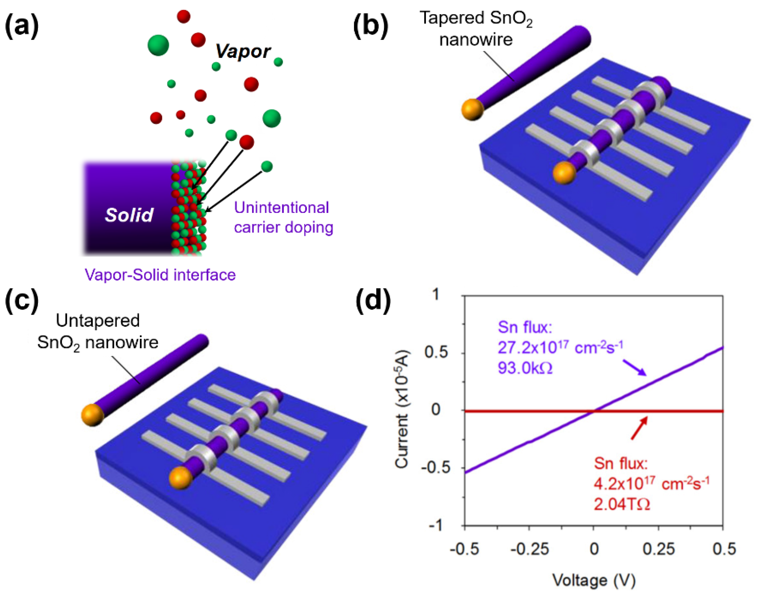
Compared with VLS growth, VS growth nanowires are suffering from insufficient ability to control uniformity, which usually results in a tapered morphology of nanowires. Recently, Anzai et al. reported a negative effect of VS growth on the tapered SnO2 nanowire electrical performance [79]. By using spatially resolved single nanowire electrical measurements, plane-view electron energy-loss spectroscopy and molecular dynamics simulations, it has been observed that the VS growth will generate a large number of defects in the oxides, thus making an unintentional doping in the nanowire structure. As shown in Figure 5d, such an unintentionally doping effect will cause a seven orders increase in the conductance, which entirely alters the intrinsic properties of nanowires. Furthermore, in light of their latest results, oxygen deficiency is the critical factor of the unintentionally doping effect in the VS growth [157]. Moreover, increasing oxygen partial pressure during the VS growth is an alternative way to prevent this drawback.
2.3. Solution Phase Growth
The solution-phase growth, for example, the hydrothermal growth, is extensively used for the synthesis of metal–oxide nanowires [64,65,158,159,160]. Compared with the vapor phase growth (both VLS and VS), a much lower temperature is required for the solution growth, which allows the nanowires to be directly integrated on the flexible organic substrates for the modern wearable device. In addition, the morphology and properties of the solution phase growth nanowires can be conveniently manipulated by tuning the concentration of the composition, introducing additional composition, or adding additives in the solvent.
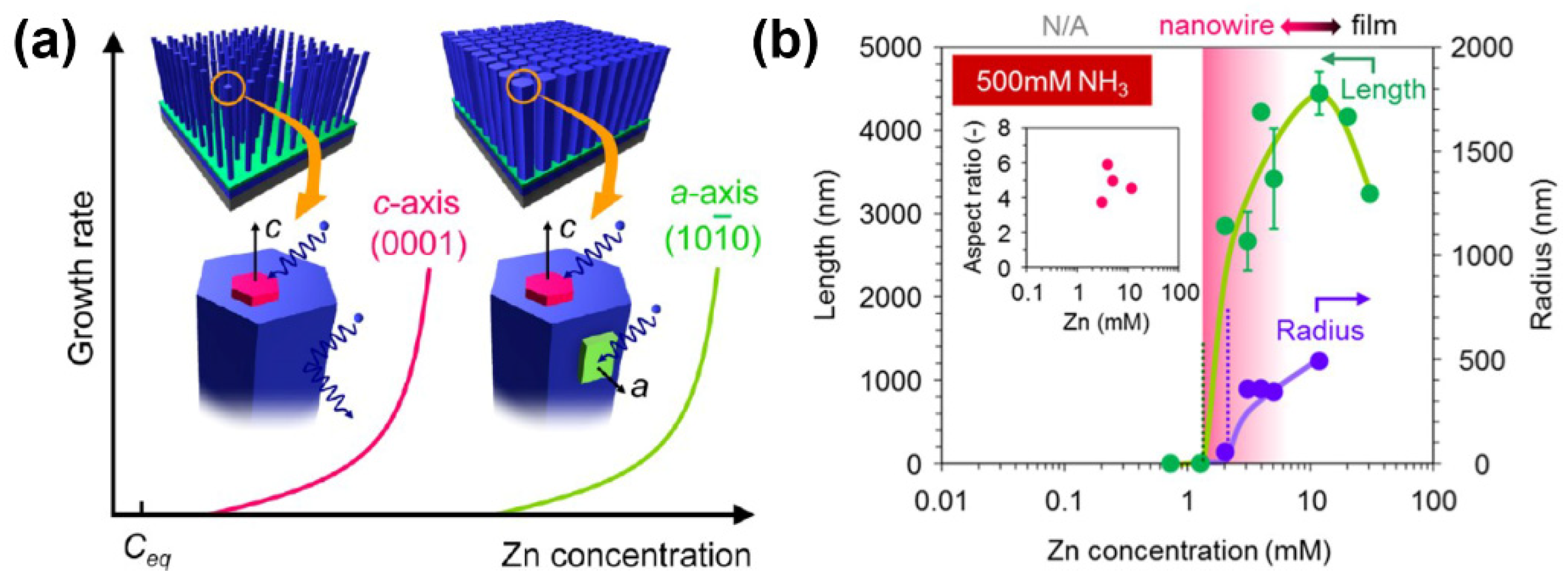
In the case of ZnO nanowires, the concept of a “concentration window” in the control of ZnO nanowire morphology has been demonstrated by He et al., as shown in Figure 6a [111]. Via carefully controlling the concentration of Zn ionic species within a specific concentration range, a selective growth on the (0001) plane can be realized. Meanwhile, under the guidance of a “concentration window”, Sakai et al. achieved a significant improvement in the growth rate of ZnO nanowires (up to 2000 nm/h) with the assistance of ammonia, as shown in Figure 6b [161]. Moreover, Joo et al. pointed out that the axial and the radial growth of ZnO nanowire can also be controlled by introducing and tuning the amount of Cd (Cu, Mg, Ca) ions or Al (In, Ga) ions in the growth solution, respectively [161]. Not only in the growth of ZnO nanowires, other anisotropic 1D nanowires can also be controlled via tuning the concentration of additives. For example, Choi et al. reported a straightforward process for synthesizing tungsten oxide nanostructure with various morphologies [162]. By changing the composition of the solvent, the crystalline phase of tungsten oxide, such as mono-clinic W18O49 nanowires (with ethanol), hexagonal WO3 platelets (with water/ethanol ratio (1:9)), and monoclinic WO3 nanosheets (with water) can be alternatively controlled. Currently, many kinds of nanowires, such as SnO2, ZnO, TiO2, In2O3, MnO2, and WO3, have been successfully synthesized via solution-phase growth with/without the assistance of the seed layer [160,163,164,165,166,167,168,169,170,171,172,173]. Owing to the low cost, less hazardous, no metal catalysts, the effectively controllable morphology and properties, the solution phase growth strategy has been successfully integrated into a well-developed micro-electro-mechanical system (MEMS) [174,175,176].
2.4. Thermal Oxidation Growth
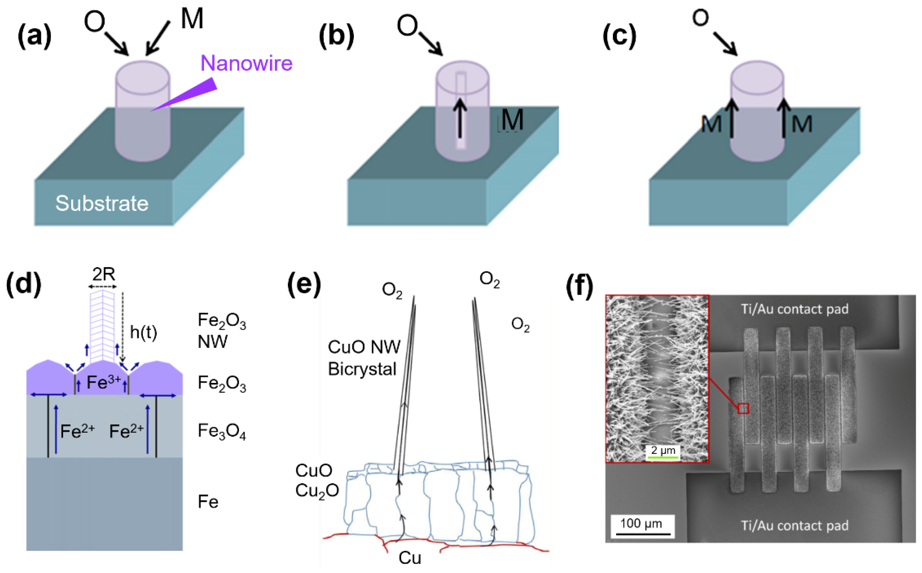
The thermal oxidation method is an easy way to massively grow metal–oxide nanowires in situ [177]. For example, Sn and Ga oxide nanowires can be easily obtained as the environment temperature increases over their melting points in the air or water vapor surroundings [31,178]. Interestingly, Zn, W, Fe, Mo, and Cu oxide nanowires can be grown by the thermal oxidation method at an even lower temperature [179,180,181,182,183,184,185,186,187]. As shown in Figure 7a–c, several possible mechanisms have been invoked to account for the thermal oxidation growth: (1) Evaporation and condensation [179,188]; (2) Fast internal diffusion along a tunnel centered on the core of a screw dislocation [180,189]; (3) Surface diffusion along the sides of nanowires [181,190]. For example, α-Fe2O3 nanowires are spontaneously grown due to the fact Fe ions tend to leave from the compressed regions at the Fe2O3/Fe3O4 interface and diffuse to the stress-free Fe2O3 surface layer, whereas CuO nanowires are basically grown due to the continuous diffusion of Cu ions from the substrate to the tip of nanowires through the internal grain boundary, as depicted in Figure 7d,e [181,189].
Owing to the in situ growth behavior of nanowires, a novel and simple technology has been reported by Steinhauer et al. for the fabrication of CuO nanowire sensors [177]. Via heating the Cu layer loaded on the patterned electrodes in air, CuO nanowires were naturally grown from the electrodes. By increasing the growth time, nanowires on foreign electrodes were mutually attached, forming the nanowire–nanowire conductive junctions as a functional sensing channel. Due to its simplicity and lack of post-processing steps after nanowire synthesis, this technique has been extensively employed to integrate CuO nanowires in a sensing device [191,192,193].
2.5. Template-Assisted Growth
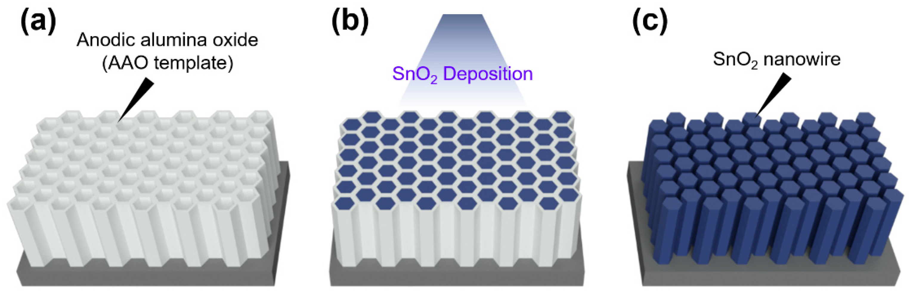
Metal–oxide nanowires can be achieved by merely depositing oxide materials into an organic template such as poly(methyl methacrylate) (PMMA) or an inorganic template such as anodic aluminum oxide (AAO). The diameter, density, and length of the nanowires can be conveniently controlled based on the template design, as shown in Figure 8. Kolmakov et al. has shown a typical inorganic template-assisted growth method to synthesize SnO2 nanowires [29]. By depositing Sn into nanoporous alumina and further etching the template by NaOH solution (or cracking by sonication), highly crystalline Sn nanowires are harvested. Then, via processing an air annealing on the metallic Sn nanowires, SnO2 nanowires are obtained.
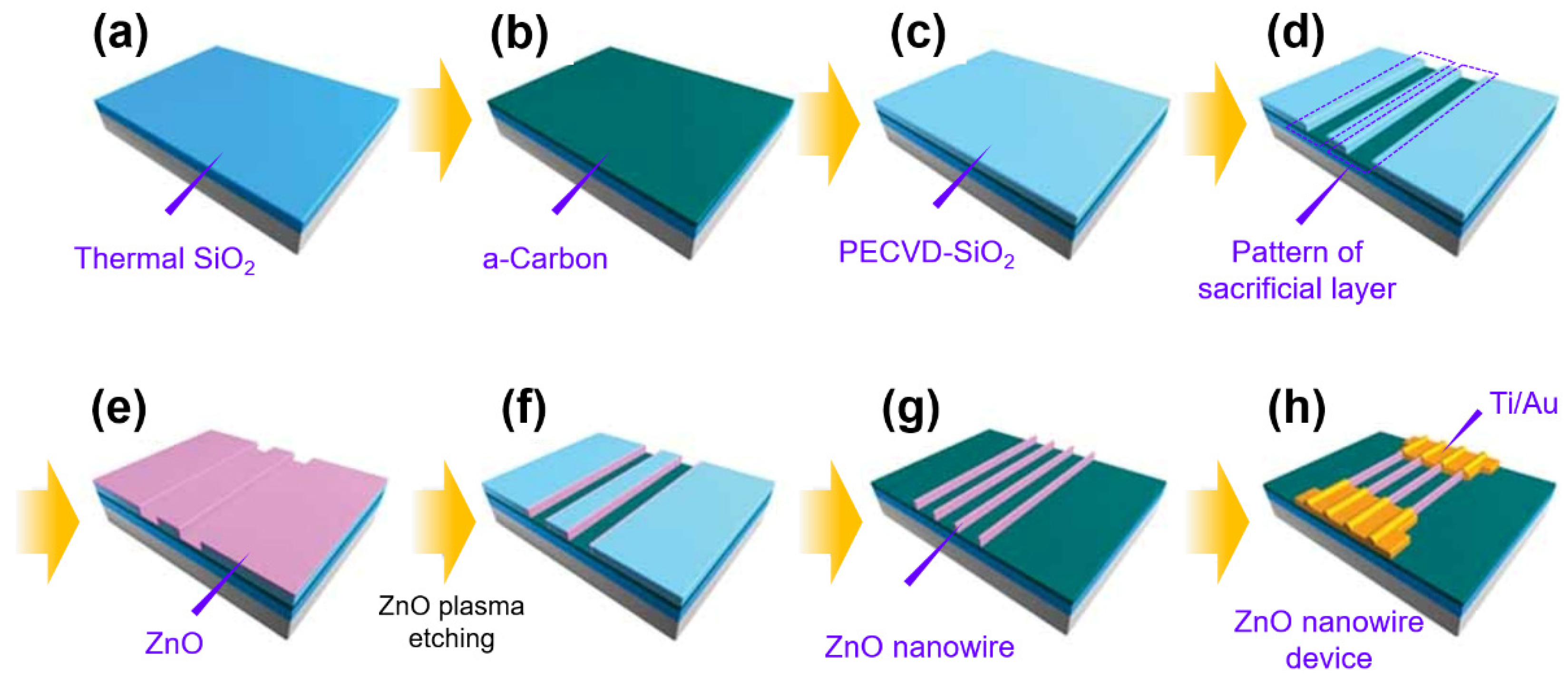
Ra et al. reported the use of an organic template for obtaining ZnO nanowires [194]. As depicted in Figure 9, a-carbon was first deposited on the SiO2/Si wafer as an etch-stop layer. Then, the wafer was coated by a sacrificial layer via plasma-enhanced chemical vapor deposition (PECVD). Then, the PECVD layer was patterned using conventional lithography and etched by the CF4/Ar inductively coupled plasma (ICP) process. Then, an atomic layer deposition (ALD) process was used to create a 70 nm ZnO layer over the pre-patterned sacrificial layer. Then, by ICP etching with Cl2/Ar discharges, the ZnO layer was removed except for the spacer part. Finally, ZnO nanowire arrays were obtained by removing the sacrificial oxide layer. A similar fabrication process for CuO, NiO, and Cr2O3 nanowires has also been recently reported [195]. Such patterning methods by using lithography techniques can prevent the problems associated with the alignment of the nanowires.
2.6. Electro-Spun Growth
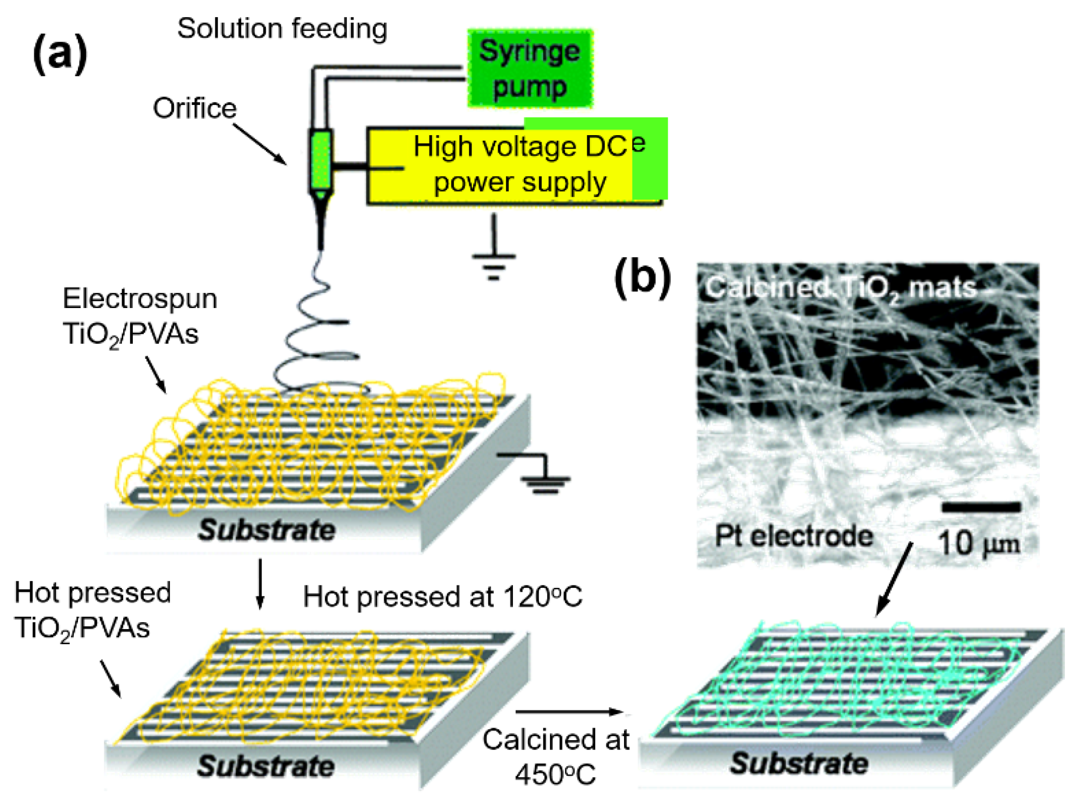
Electro-spinning is one of the easiest, template-free, versatile, and cost-effective approaches to produce 1D nanostructures. Almost all the oxides and mixed oxides nanowires can be fabricated using this method [196,197,198,199,200,201,202,203,204,205,206,207,208,209,210]. Figure 10 shows a typical example of nanowires/nanofibers fabrication by electro-spun growth [201]. As shown in Figure 10a, an appropriate ratio of dimethylformamide, poly(vinyl acetate) (PVA), titanium(IV) propoxide, and acetic acid are mixed as the precursor solution. Then, the solution is loaded into a syringe, which is connected to a high-voltage supply. Afterward, the precursor solution was directly spun onto the Al2O3 substrate with pre-patterned Pt electrode arrays. Finally, nanofibers are pressed under 120 °C to prevent sticking and further calcined in air at 450 °C, and thus TiO2 nanofibers sensors with the mat-like structure are obtained. Due to the simple and inexpensive fabrication process, electrospinning has attracted increasing attention in the commercial field.
3. Metal–oxide Nanowire Devices Fabrication
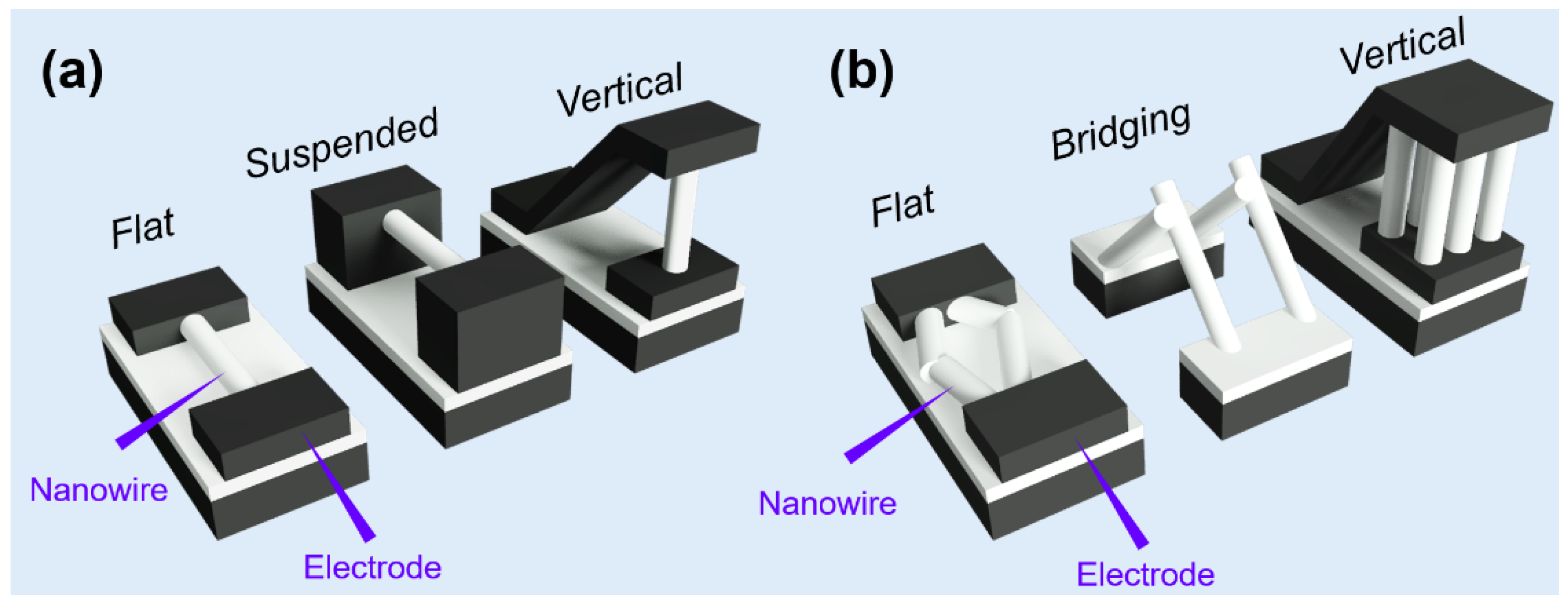
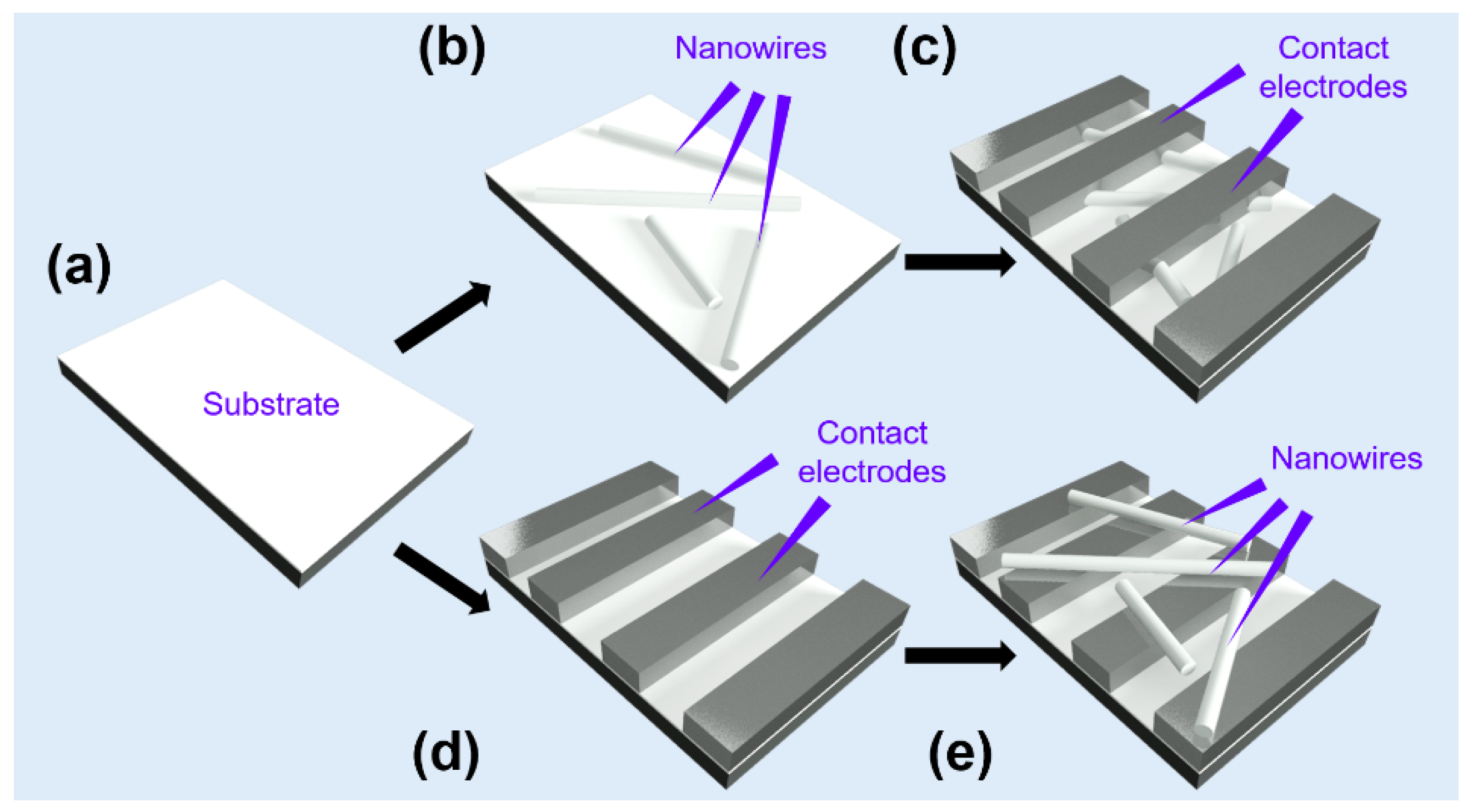
To study the intrinsic properties of nanowires and use their functionality as a sensing element, one necessary process is transferring nanowires from the growth substrate and integrating them with contact electrodes on a platform. As shown in Figure 11, the current nanowire-based device can be divided into two types: (a) individual nanowire device; and (b) multiple nanowire devices.
3.1. Individual Metal–Oxide Nanowire Device
Due to the fast development of modern electronics, individual metal–oxide nanowire devices such as the field-effect transistor (FET) offer a great chance to explore the electrical, chemical, and mechanical properties of the nanowire.
3.1.1. Device with Flat Structure
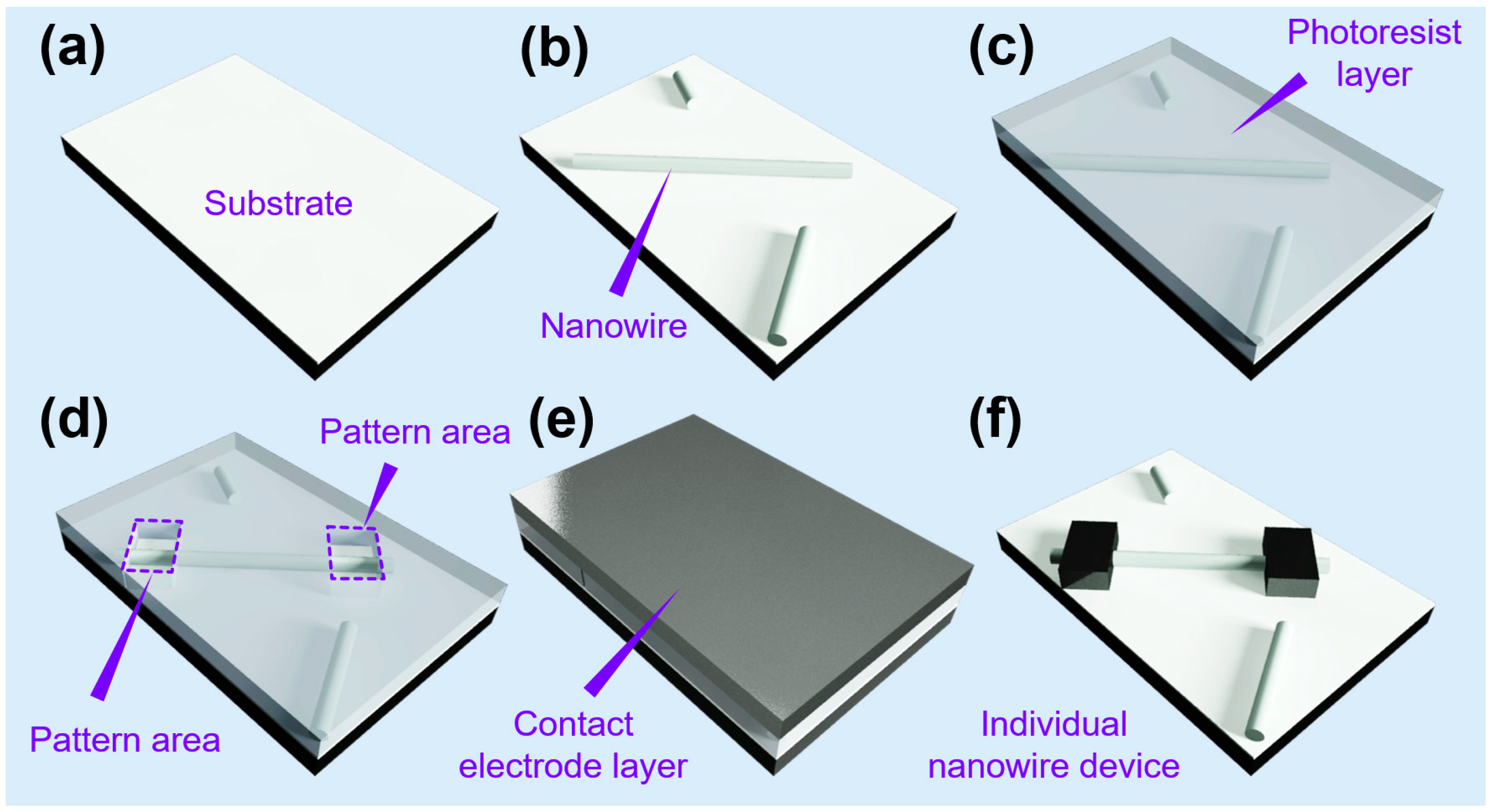
A “pick and place” is a common technique in fabricating individual nanowire devices. First, one must “pick” metal–oxide nanowires from the growth substrate. The substrate with nanowires should be immersed in a readily volatile solvent such as isopropanol, ethanol, methanol, and even water. Then, the metal–oxide nanowires are transferred from the growth substrate and dispersed into solvents under the ultrasonic wave. One must then ‘place’ the nanowires. One drop of solvents containing dispersed nanowires should be placed on the platform with pre-deposited electrode pads and dried by simple evaporation. With the assistance of optical scope or SEM observation, the relative positions of nanowires to the pre-deposited markers are recorded. Then, the platform should be covered with a layer of photoresist by spin coating technique. By combining laser/electron-beam lithography and sputtering deposition (or using focused ion beam technique), nanowires can be connected with the electrode pads. Finally, the additional metal and photoresist can be removed by a lift-off process in the organic solvent such as N-methyl-2-pyrrolidone (NMP), dimethylformamide (DMF), and ethanol. The schematic image of the individual nanowire device fabrication process can be seen in Figure 12. Other novel fabrication processes can be seen in the latest review [211].
3.1.2. Device with Suspended Structure
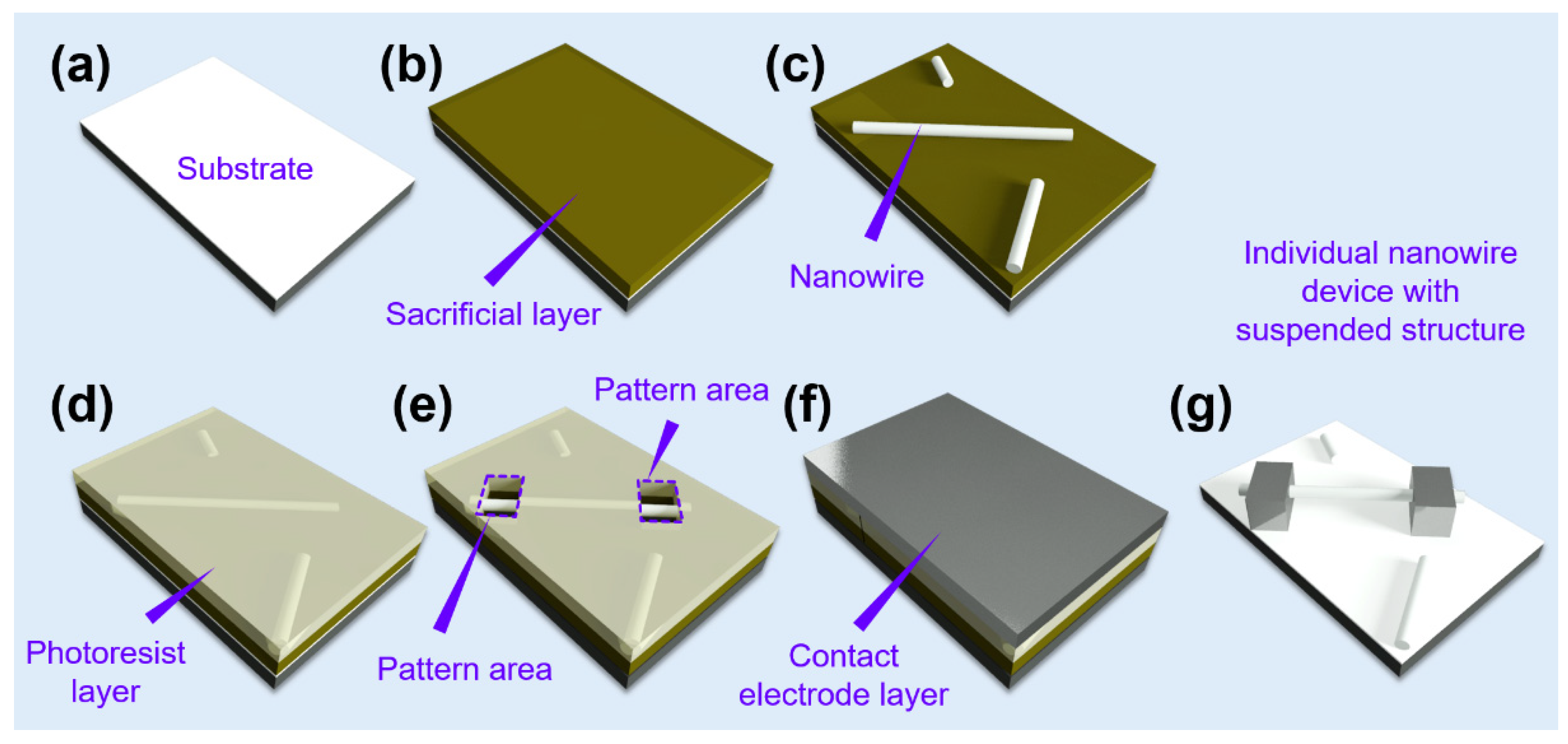
Due to the sensor heating, the hot air near the sensor surface will form a layer which is likely to support convective processes leading to the concentration gradients of reactive analyte gases, termed as stagnant layer [212]. Such a layer can measure up to several tens of nanometers, and it is comparable with the nanowire size, which will cause insufficient exposure to the target molecules [213,214]. To prevent this problem, a suspended structure has been developed to improve sensor performance. The suspended structure is a highly favorable configuration because the nanowires are surrounded by the gas atmosphere. As shown in Figure 13, the fabrication process of a suspended nanowire device is similar to that of a flat nanowire device. However, it requires one more sacrificial layer (inorganic MgO/organic PMMA) before the drop of nanowire solvent (Figure 13b). The overall enhancement in the performance of the nanodevice is benefited from the suspended structure. For example, Nima et al. fabricated a stable, reproducible ZnO nanowire humidity sensor with a suspended structure [215]. It is observed that the suspended nanowire device presented an exponential change (over five orders) of resistance in response to relative humidity from 0% (dry air) to 60% at room temperature. This improvement is strongly associated with a subthreshold carrier modulation in the nanowire core, the high surface-to-volume ratio of the nanowire, and most importantly, complete exposure of the nanowire surface to air. Owing to the gigantic enhancement in gas sensing response, the development of metal–oxide nanowire gas sensors with the suspended structure has been extensively studied [214,216,217,218,219,220].
3.1.3. Device with Vertical Structure
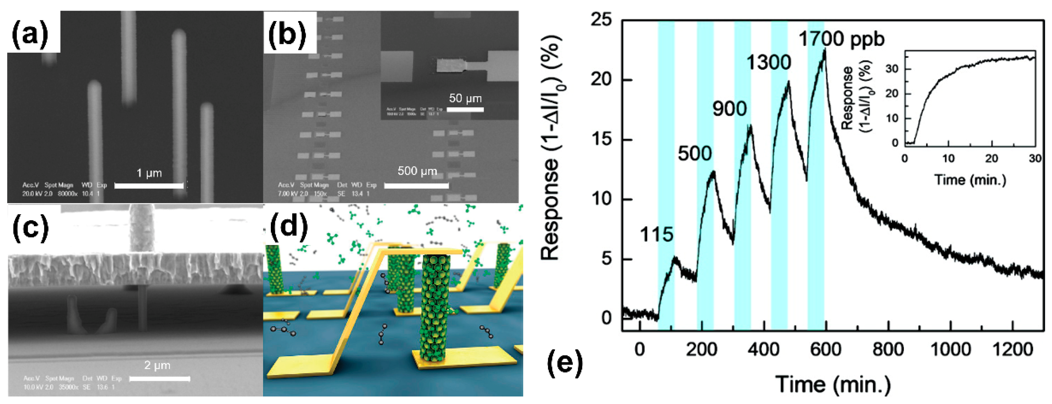
Similar to the suspended nanowire device, sensors with a vertical structure have also been considered a promising design for gas detection due to their 3D architecture. Unfortunately, the conventional “pick and place” technique cannot obtain individual nanowire devices with vertical structures due to the current limitation in nanotechnology. To date, a few papers reported the individual nanowire sensor devices with a vertical structure [221,222]. Offermans et al. offered a potential way to achieve the individual nanowire gas sensor with vertical structure [223,224]. As shown in Figure 14, vertical indium arsenide (InAs) nanowires are firstly grown on an InP(111)B wafer. Then, the nanowires were patterned into arrays ranging in size from 30 μm × 30 μm to 100 μm × 100 μm via combining the sacrificial resist layer and etching process. Finally, using the sacrificial resist layer with sputtering deposition, air bridges were formed to make electrical connections. In view of their device structure, it is possible to achieve a device with fewer nanowire connections or even a single nanowire connection by shrinking the size of the patterned array. Meanwhile, it was shown that this vertical structure of the sensor device presents a very high sensitivity to 100 ppb of NO2 at room temperature. However, due to the uncertainty and complexity of this process, it is impossible to massively fabricate such a device with individual vertical nanowires. To the best of our knowledge, to date, there has been no report using individual metal–oxide nanowires with vertical structure as the gas sensor.
3.2. Metal–Oxide Multiple Nanowire Device
Due to the requirement of precise alignment between the single nanowire and pre-deposited patterned electrodes, the overall fabrication process of the individual nanowire device is complicated, time-consuming, and expensive [225,226,227,228,229]. Furthermore, high accuracy and stable electrical measurement systems are needed to obtain the electrical sensing signals of the single nanowire sensor devices [75]. To simplify the fabrication process and electrical signal measurement, multiple nanowire devices become the most widely accepted device design in practical sensor device applications.
3.2.1. Device with Flat Structure
A mat-like nanowire structure is similar to the single nanowire device with a flat structure, while the fabrication process is much easier than that of the single nanowire device. In a typical mat-like structure, the device can be loaded easily via two steps. As shown in Figure 15, nanowires can be firstly transferred from the growth substrate onto a platform, and then the contact electrodes are deposited by utilizing a mask with sputtering. Alternatively, the electrodes can be firstly pre-deposited on the platform, and finally nanowires are transferred on the surface of electrodes. Both of the two methods are simple, costless, and unnecessary pre/post-process. Due to its convenience in terms of fabrication process, various metal–oxide nanowire gas sensors, including SnO2, ZnO, WO3, TiO2, NiO, CuO [230,231,232,233,234,235], are successfully obtained by this method. Moreover, this technique is in favor of flexible sensor electronics integration.
3.2.2. Device with Bridging Structure
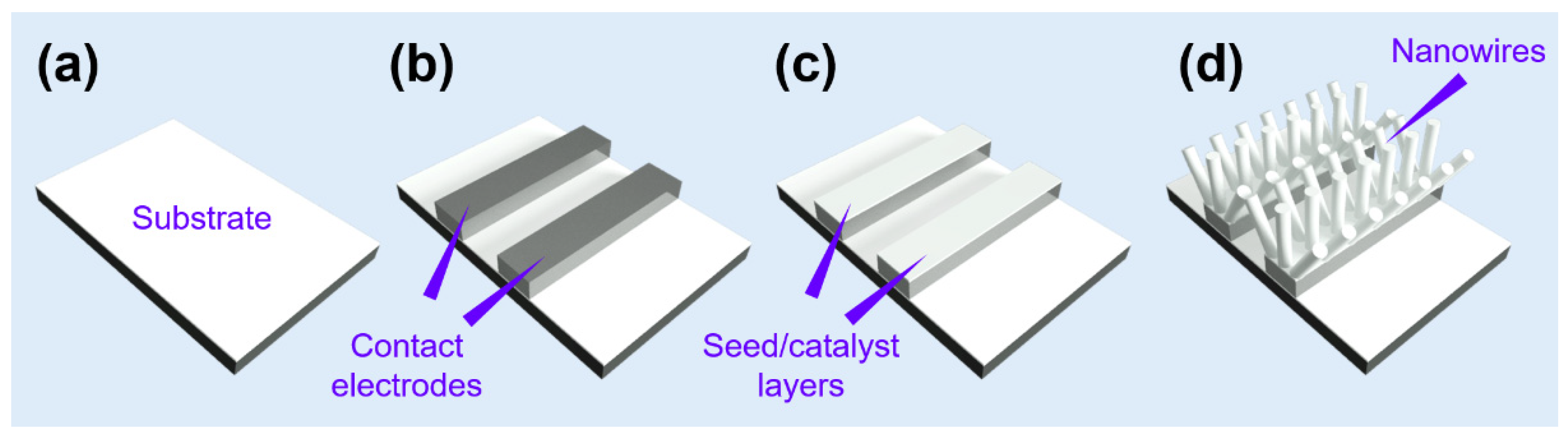
Due to the easy fabrication, in situ controllable nanowire growth position, and 3D architecture, bridging structure is another promising design for nanowire gas sensors [43,177,191,192,193,236,237,238,239,240,241,242,243,244,245,246,247,248,249,250,251,252,253,254,255,256,257,258,259,260,261,262,263,264,265,266,267]. In the typical fabrication process of the device with a bridging structure, bottom electrodes should be firstly deposited on the substrate, then a seed/catalyst layer will be deposited on the top of the bottom electrodes. Finally, nanowire will be grown in situ only on the seed/catalyst layer, as shown in Figure 16. With the increase in the growth time, nanowires will incline and contact other nanowires, forming nanowire–nanowire junctions, which can be utilized as a sensing channel for gas detection. Such on-chip growth nanowire sensors can prevent nanowire–electrode contact issues encountered by the flat nanowire sensor devices, and these kind of sensors show a more stable physical and electrical performance than the sensors fabricated by spinning, dropping, or spray coating technique. Park et al. firstly reported a comparison study of NO2 sensing between air-bridged nanowire sensors and conventional nanoparticle sensors [251]. Owing to a higher exposed area to the surroundings, the bridging structure shows a faster response and recovery rates as compared with that of nanoparticle sensors. Meanwhile, Kim et al., Jung et al., and Hung et al. systematically studied the effect of nanowire junction density on the device sensing performance [245,253,260]. Through the controlling of nanowire growth time, the number of nanowire–nanowire junctions within the bridging sensor structures can be quantitatively manipulated. Furthermore, it was found that the bridged structures with a high density of junctions show a high sensing performance to NO2. However, the response and recovery time of the bridging nanowire device with a high density of junctions are slower than that of the low-density nanowire device, because a long time is needed for the molecules’ diffusion in the high density of nanowire network.
3.2.3. Device with Vertical Structure
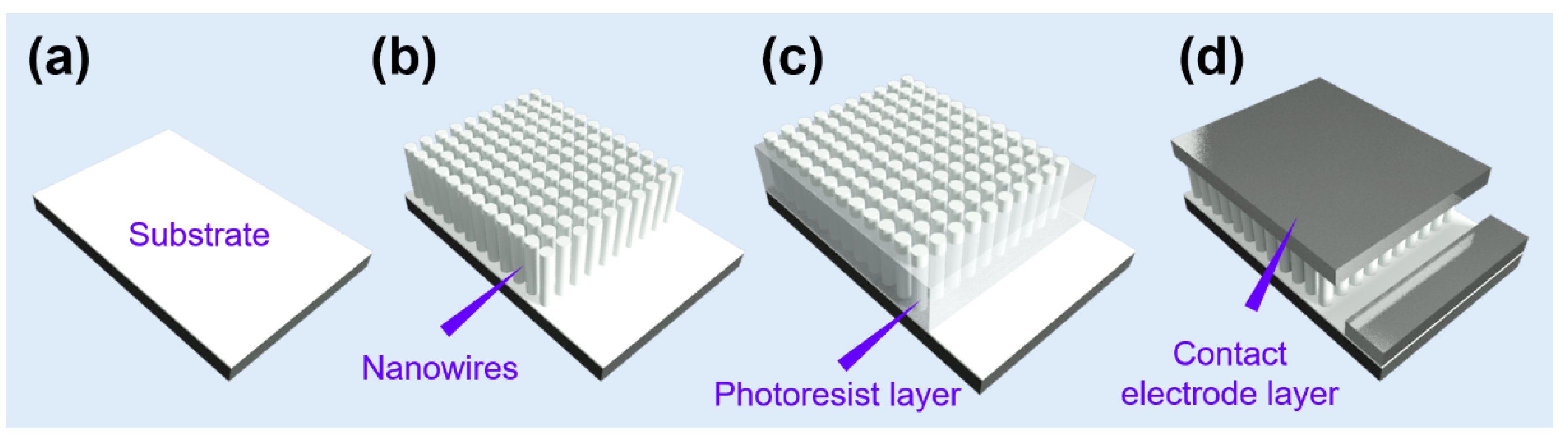
Recently, the nanowire array sensors with the vertical structure are promising due to their porosity structure and reliable electrical performance [268,269,270]. To obtain a vertical nanowire sensor, three steps are typically needed, as shown in Figure 17. First, nanowires are grown vertically on the substrate through solution–phase/vapor–phase methods. Then, the nanowires are covered by spin coating a layer of organic photoresist. By precisely controlling the thickness of photoresist on a nanowire array via etching process, the tips of nanowires will be exposed. Afterwards, a metal contact layer is deposited onto the photoresist and connected with all the tips of the nanowires. Finally, a vertical structure of the sensor device can be achieved by removing the unnecessary photoresist. Cao et al. has demonstrated the integration of a vertical WO3 nanowire sensor with high sensitivity to NO2 [268]. It is shown that the vertical device exhibited the capability to detect NO2 concentrations down to the 50 ppb level, which shows a promising future in the field of low concentration gas detection. In addition, Chen et al. has proposed a sensor array composed of vertical device structures with different noble metal decorations (Pd, Pt, and Au) for selective gases detection [48]. Several different types of sensors are fabricated via altering the selection of decorating materials.
4. Current Progress in Performance Tailoring of Metal–Oxide Nanowire-Based Gas Sensors
Although metal–oxide nanowires have already shown great potential as gas sensing materials, further efforts are still encouraged to enhance the sensing performance of nanowire-based sensor electronics, such as gas species discrimination from mixtures, low concentration, and room temperature detection. To achieve such goals, introducing additives on the nanowire surface has been proved to be an easy and effective approach.
4.1. Nanoparticles Decoration (NPs Decoration)
The loading of noble metal/oxide nanoparticles with a nanometer size onto a metal–oxide nanowire surface has been widely employed for functionalizing the nanowire-based sensors due to their low cost and simplicity in the fabrication process. Here, we introduce one common method (not least) to load nanoparticles on nanowires. For noble metal nanoparticle decoration as an example, a noble metal (M) precursor solution was firstly prepared by dissolving appropriated HMClx·H2O into H2O (ethanol, etc.). Then, by simply immersing nanowires in the above solution for a proper time and calcined at high temperature, M-loaded nanowires can be obtained. This method can also be used for metal–oxide nanoparticle decoration, despite using different precursors. Currently, there are two coexisting mechanisms to understand the sensing performance of decorated nanowires: (1) chemical sensitization (spillover effect): noble metal nanoparticles can promote the dissociation of molecules and oxygen on nanowire surface, leading to an efficient chemical reaction. Moreover, owing to the noble metal-induced lower energy barrier for gas adsorption and desorption, the response and recovery rates can be accelerated [271]; (2) electronic sensitization: the interface between oxidized noble metals (or oxide nanoparticles) and nanowires usually form a thicker electron depletion layer with a narrow channel. During exposure to the target molecules, the concentration of charge carriers can be efficiently modulated [272]. To date, researchers have made significant progress in fabricating nanoparticles decorated nanowire sensors. Through optimizing the decorated material selection/combination, the size of nanoparticles, and the surface coverage of nanowires, it is accessible to realize the fabrication of functionalized nanowire sensors with high sensitivity, high selectivity, and low working temperature. A detailed overview of the sensing performance of noble metal-decorated metal–oxide nanowire gas sensors is summarized in Table 1.
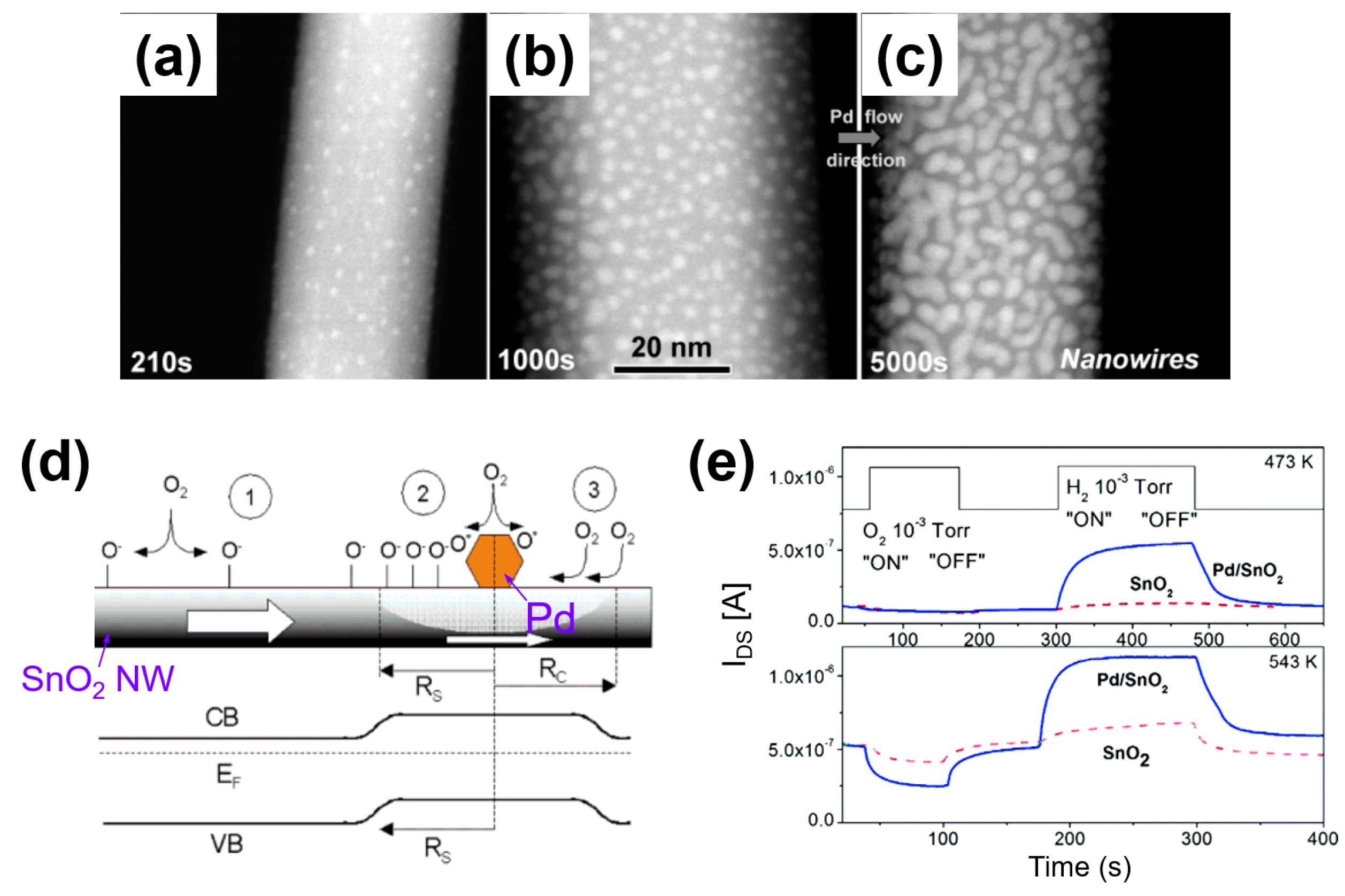
As for sensitivity, Kolmakov et al. firstly reported the use of noble metal (Pd) functionalized with metal–oxide nanowire (SnO2) device for the sensitivity enhancement [273]. As shown in Figure 18 d, due to (1) oxygen dissociation on Pd nanoparticles by spillover effect, and (2) the diffusion of weakly adsorbed oxygen on nanowire surface to Pd nanoparticles, it is found that the Pd nanoparticles decoration can dramatically enhance the device sensing performance to O2 and H2. Motivated by this encouraging result, to date, tremendous efforts via noble metal/oxide nanoparticles decoration are being intensively investigated for enhancing device sensitivity [87,273,274,275,276,277].
Nanoparticle decoration is also an alternative way to dramatically improve the selectivity of the nanowire-based sensors [174,272,274,275,276,277,278,279,280,281,282,283,284,285,286]. For example, Kim et al. reported a ZnO nanowire sensor with high sensitivity and selectivity toward H2 via Pd nanoparticle decoration [274]. Due to the synergistic effect of chemical sensitization of Pd nanoparticles and metallization effect of ZnO, the sensing response to H2, O2, NO2, C6H6, and C7H8 are increased by 3214.1, 1.6, 7.8, 17.2, and 166.9%, respectively. Moreover, compared with pristine nanowire, the Pd-decorated ZnO nanowire shows a capability to detect 0.1 ppm H2 with a wide temperature range from 150 to 350 °C. Byoun et al. reported a TeO2 nanowires gas sensor by surface decoration with oxide nanoparticles [280]. Due to the formation of p–n heterojunctions between p-type TeO2 nanowire and n-type ZnO nanoparticles, the TeO2 nanowires become more resistant and suitable for sensing oxidizing gas, especially since it shows an excellent NO2 selectivity in comparison with interfering gases such as SO2, CO, and C2H5OH.
Furthermore, surface decoration with noble metal/oxide nanoparticles has been regarded as an effective way in lowering down the sensor operation temperature [280,287,288,289,290,291,292,293,294,295]. For example, as reported by Liang et al., due to the spillover effect and the change in depletion layer caused by Au nanoparticles, the Au decorated VO2 nanowires sensor exhibits an excellent sensing performance to NO2 at 0.5–5 ppm at room temperature [285]. Lupan et al. have reported that Au nanoparticle decoration on ZnO nanowire surface can realize the H2 room temperature detection [289], Choi et al. found that Pd nanoparticles decoration on ZnO nanowires enables the CO sensing at room temperature [287] and Hong et al. have reported the Cu2O nanoparticles-decorated ZnO nanowire sensor could realize the room temperature sensing of NO [296].
In addition, the effects of decorated nanoparticle size and density have also been intensively investigated [192,271,282,296,297]. For example, Lee et al. have studied the size effect of Au nanoparticles on the CuO nanowire sensor [192]. As the diameter of Au nanoparticles decreases, the sensing responses of the nanowire sensor present an increase to NO2 and CO, and a maximum performance appears when 60 nm of Au nanoparticles are decorated on the CuO nanowire surface. Meanwhile, they have pointed out that the size of nanoparticles should be carefully optimized to prevent sufficient surface coverage, since excessive surface coverage would cause the steric hindrance on the nanowire surface, which is harmful to gas sensing.

Table 1.
A detailed overview of sensing performance of noble metal-decorated metal–oxide nanowire gas sensors.
Table 1.
A detailed overview of sensing performance of noble metal-decorated metal–oxide nanowire gas sensors.
| NWs | NPs | Target Gas | Toper, (°C) | LOD (ppm) | Response | Response Time(s) | Ref. |
|---|---|---|---|---|---|---|---|
| SnO2 | Ag | NH3 | 450 | 0.05 | 300 @ 100 ppm | 45 | [298] |
| Au | NO2 | 200 | 0.1 | 2 @ 0.1 ppm | N/A | [299] | |
| Au/ZnO-branching | NO2 | 300 | 2 | 13 @ 10 ppm | 118 | [300] | |
| Au/ZnO-shell | CO | 300 | 0.0026 | 26.6 @ 0.1 ppm | 75 | [301] | |
| Pd | H2 | 300 | 1 | 55.72 @ 100 ppm | 22 | [302] | |
| Pd | NO2 | 300 | 0.1 | 505 @ 0.1 ppm | 20 | [271] | |
| Pd | H2 | 300 | 1 | 16.95 @ 1 ppm | N/A | [88] | |
| Pd | H2 | 150 | 10 | 4.5 @ 100 ppm | N/A | [303] | |
| Pt | NO2 | 300 | 0.1 | 700 @ 0.1 ppm | 10 | [271] | |
| Pt | H2 | 25 | N/A | 1.87 @ 1000 ppm | 0.33 | [288] | |
| Pt | Ethanol | 300 | 0.1 | 6.5 @ 100 ppm | N/A | [304] | |
| Pt | Benzene | 350 | 0.1 | 18 @ 100 ppm | N/A | [304] | |
| Pt | Acetone | 300 | 0.1 | 5.8 @ 100 ppm | N/A | [304] | |
| Pt | H2 | 350 | 0.1 | 4 @ 100 ppm | N/A | [304] | |
| Pt | Toluene | 300 | 0.1 | 58 @ 100 ppm | N/A | [304] | |
| ZnO | Pd | Ethanol | 260 | - | 5 @ 500 ppm | 6 | [305] |
| Ag | Ethanol | 450 | 5 | 228.1 @ 100 ppm | 40–80 | [306] | |
| Au | NO2 | 150 | 1 | 31.4 @ 1 ppm | 29 | [284] | |
| Au | NO2 | 25(UV) | 1 | 2.6 @ 1 ppm | 39.5 | [292] | |
| Au | H2 | 25 | <1 ppm | 40 @ 100 ppm | N/A | [289] | |
| Au | Acetone | 172 | 15 | 50.5 @ 100 ppm | 1 | [307] | |
| Au | H2 | 25 | 20 | 32.9 @ 1000 ppm | N/A | [282] | |
| Au/Fe2O3 | NO2 | 400 | 150 | 247 @ 250 ppm | N/A | [308] | |
| Au/Pd | NO2 | 100 | 1 | 94.2 @ 1 ppm | 35 | [309] | |
| Pd | Benzene | 25(UV) | 0.0067 | 2.2 @ 50 ppm | N/A | [310] | |
| Pd | H2 | 350 | 1 | 87 @ 100 ppm | N/A | [274] | |
| Pd | H2S | 300 | 10 | 20 @ 500 ppm | 720 | [311] | |
| Pd/BN | H2 | 200 | 0.1 | 12.3 @ 50 ppm | 240 | [307] | |
| Pt | H2S | 260 | 0.0011 | 65 @ 0.3 ppm | 40 | [312] | |
| Pt | Toluene | 25(UV) | 0.0003 | 2.86 @ 50 ppm | N/A | [310] | |
| WO3 | Au | n-butanol | 250 | 5 | 147 @ 100 ppm | 16.5 | [313] |
| Au | Acetone | 250 | 5 | 72 @ 200 ppm | 17.5 | [313] | |
| Pd/Au | Acetone | 300 | 200 | 152.4 @ 200 ppm | 96 | [314] | |
| Pd/Au | n-butanol | 200 | 5 | 93 @ 50 ppm | 12 | [315] | |
| Rh | Acetone | 300 | 0.2 | 75 @ 5 ppm | 11 | [316] | |
| Ru | Acetone | 350 | 0.05 | 78 @ 5 ppm | 11.7 | [202] | |
| W18O49 | Ag/Pt | Trimethylamine | 240 | 0.071 | 22 @ 2 ppm | 15 | [277] |
| In2O3 | Ag | Ethanol | 25 | 0.5 | 1900 @ 100 ppm | N/A | [317] |
| Au | CO | 25 | 0.5 | 2200 @ 100 ppm | N/A | [317] | |
| Pt | H2 | 25 | 0.5 | 1400 @ 100 ppm | N/A | [317] | |
| CuO | Au | NO2 | 300 | 1 | 2.2 @ 50 ppm | N/A | [192] |
| Au | CO | 350 | 1 | 1.25 @ 50 ppm | N/A | [192] | |
| Pt | Ethanol | 200 | 1000 | 3.8 @ 1000 ppm | 480 | [318] | |
| Pd | H2 | 200 | 1000 | 4.5 @ 1000 ppm | 600 | [318] | |
| Pd | H2S | 100 | 1.9 @ 100 ppm | N/A | [319] | ||
| PdO | Pt | H2 | 25 | 10 | 1.2 @ 100 ppm | 166 | [290] |
| VO2 | Au | NO2 | 25 | 0.5 | 3.22 @ 5 ppm | N/A | [285] |
NWs: nanowires; NPs: nanoparticles; Toper: operation temperature of sensor; LOD: limit of detection); Response: Rg/Ra (Oxidizing gas) or Ra/Rg (Reducing gas).
4.2. Branched Nanowire
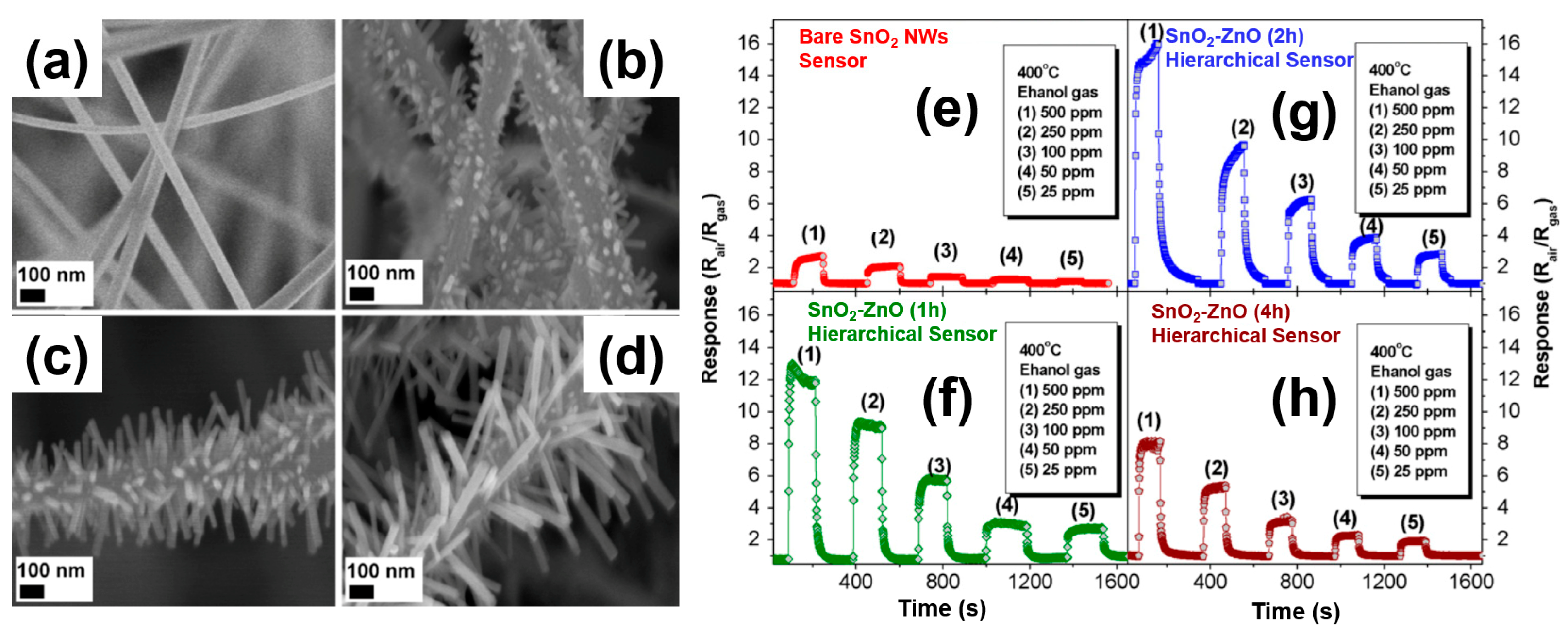
In addition to surface decoration, branched nanowires (nanowire hierarchical nanostructures) offer a high specific surface area for gas diffusion and adsorption, which are beneficial for molecular sensing. Khoang et al. reported a controllable and scalable route for preparing n-type ZnO branched n-type SnO2 nanowire hierarchical nanostructures via a combination of thermal evaporation method (SnO2 nanowires) and hydrothermal method (ZnO nanowires). As shown in Figure 19, compared with pure SnO2 nanowires, the branched nanowires sensor shows three–five-fold sensitivity enhancement to 25–500 ppm ethanol. Kaur et al. demonstrated an n-type ZnO branched p-type NiO nanowire hierarchical structures for sensing performance enhancement [233]. In such a kind of sensor, the surface of NiO nanowires is fully covered by ZnO nanowires, leading to a response mode transformation from the p-type to n-type. In addition, the lowest detection limits of these sensors to ethanol and acetone can be down to 7 and 11 ppm, respectively.
Moreover, to further improve the device sensing performance, Choi et al. attempted to decorate Au nanoparticles on the ZnO branched SnO2 nanowire surface [300]. It was indicated that the sensing response of the ZnO-branched SnO2 nanowire sensor is dramatically enhanced after Au nanoparticle decoration due to the spillover effect of noble metal. Meanwhile, the sensor shows an excellent selectivity toward NO2. Similar results have also been reported recently by Bang et al. [320]. They realized the low temperature and selective NO2 sensing via using synergistic effects of Pt decoration and Bi2O3 branching.
Figure 19.
Left figure: branches nanowire with different length on ZnO nanowires: (a) as fabricated ZnO nanowires; (b) 1h growth SnO2 branched ZnO nanowire; (c) 2 h growth; (d) 4h growth. Right figure: SnO2 nanowire and SnO2–ZnO hierarchical structure sensing performance; (e) as fabricated ZnO nanowires; (f) 1h growth SnO2 branched ZnO nanowire; (g) 2h growth; and (h) 4h growth. Reprinted from reference [321] with permission from the American Chemical Society.

4.3. Core–Shell Structure (C–S Structure)
Core–shell (C–S) metal–oxide nanowire sensors have also been extensively studied due to their ability to detect an extremely low concentration of chemical species and mitigate the poor selectivity [322,323]. The C–S structure is similar to the nanoparticle-decorated structure but with a continuous layer and higher stability [271]. Such a shell layer can serve as a catalytic layer to promote the molecular oxidizing [324], narrow the conduction core part of nanowire [325], facilitate the adsorption of gas molecules to increase the sensing activity [326], and work as a main conductive channel for sensing [327]. Currently, various C–S nanowires with a combination like n–n (n-type core/n-type shell) [323,327,328,329,330], n-p (n-type core/p-type shell) [256,331], and p-n (p-type core/n-type shell) [252,324,332] have been employed as gas sensors. According to recent C–S nanowire gas sensors, the shell layer selection and its deposition thickness are crucially important to tailor the performance of the nanowire-based gas sensors [332,333].
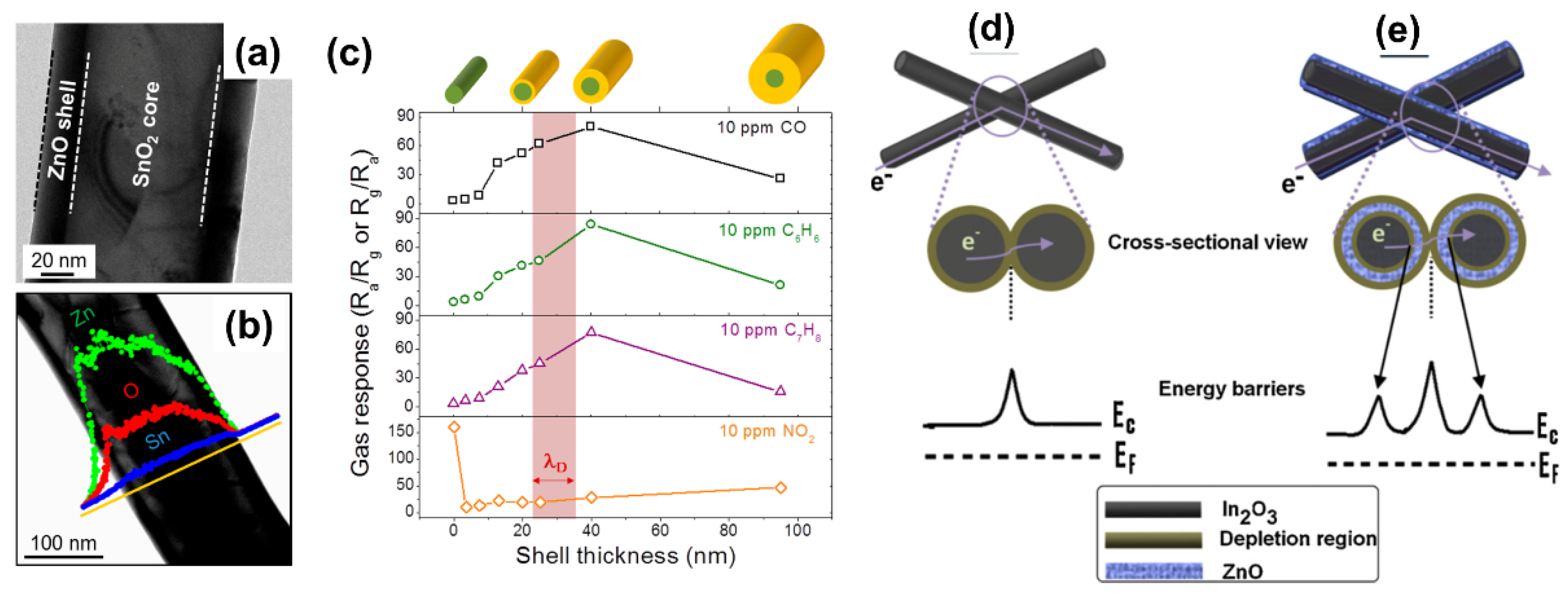
Park et al. firstly demonstrated an exciting model to understand the sensitivity enhancement in SnO2-ZnO C–S nanofibers [328]. As the deposition shell thickness is comparably shorter than or equivalent to the Debye length of the shell materials, the conducting channel can be fully depleted during the exposure to target molecules. As a result, the conductance variation is favorably considerable compared with that of the non-C–S structure. Katoch et al. also reported a similar result via systematically studying the impact of shell thickness on the sensing performance of core/shell structures [330]. By gradually changing the thickness of ZnO on SnO2 nanofibers, it was observed that the nanofiber sensor device has the highest sensing response towards CO when 20 nm of ZnO shell is loaded on the SnO2 nanofiber surface. Such thickness is identically close to the Debye length of ZnO.
As shown in Figure 20a–c, by controlling the ALD growth time of the shell layer, Choi et al. proposed a dual functional sensing mechanism in the SnO2/ZnO C–S nanowires [327]. First, as the shell layer is thinner than its Debye length, the shell layer will experience a large resistance modulation during the sensor exposure to reducing gas. As a result, a substantial portion of electron transport occurs through the inner core nanowire, which would weaken its sensing performance. Second, as the shell layer is slightly larger than its Debye length, electrical transport will be mostly confined within the shell layer, leading to a high modulation/response in sensing performance.
Singh et al. have discussed carrier transport based on In2O3 nanowires and In2O3/ZnO core–shell nanowires network devices [334]. Due to the large resistance of the polycrystalline ZnO shell, carriers mainly flow through the single crystalline In2O3 core. To achieve electron transportation from nanowire to nanowire, only one potential barrier (core–core, C/C) has to be overcome in the In2O3 nanowires device (Figure 20d), while the electrons are essentially to overcome three potential barriers (core to shell (C/S), shell to shell (S/S), and shell to core (S/C)) in the core–shell nanowire devices (Figure 20e). Owing to the modulation of potential barriers, significant enhancements in sensor response for the reducing gases have been achieved. This mechanism also can be used to explain the sensing performance enhancement in other p/n and n/p types of core/shell nanowire sensors [256,325,329,331,335].
4.4. Impurities Doping
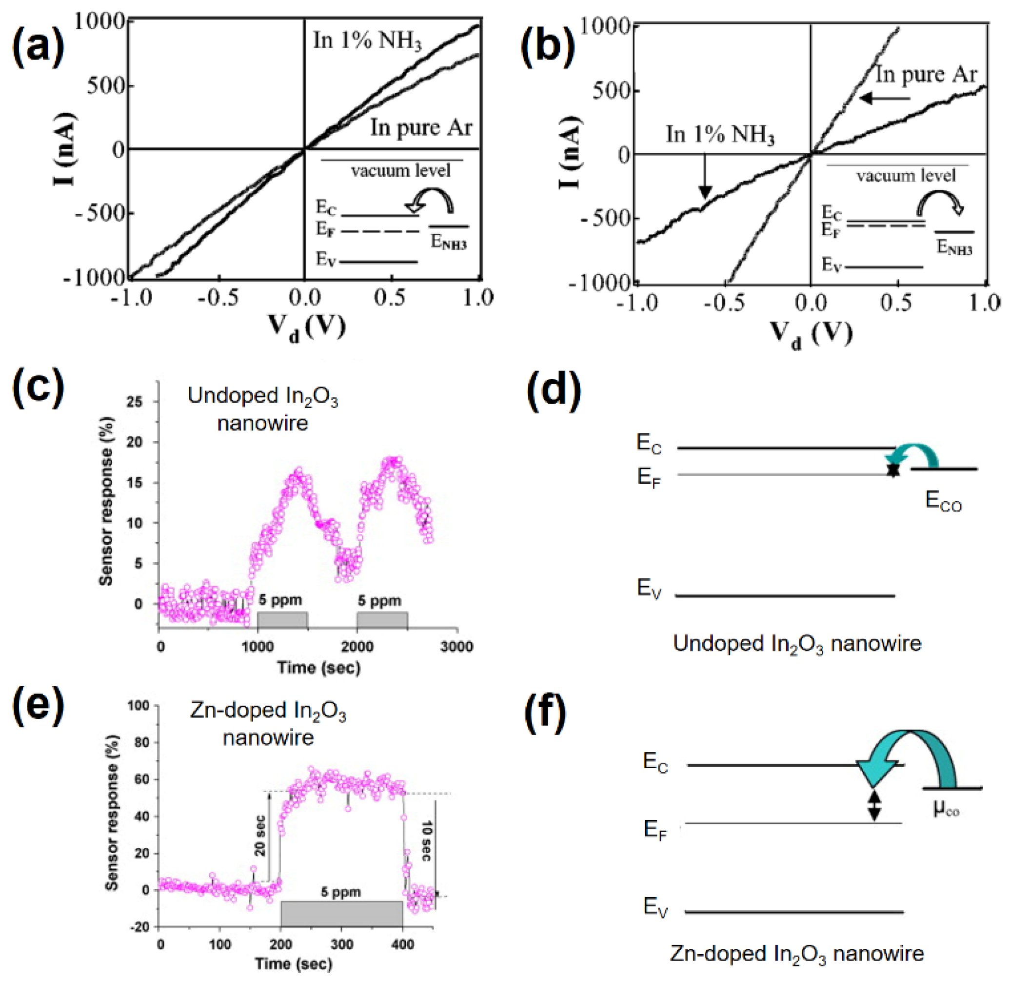
Introducing dopants have a significant impact on the electrical and chemical properties of semiconductor metal–oxides [336,337,338]. Experimental studies have proved that small amounts of impurity additives (< 0.1 at% or lower) can significantly alter the electronic and chemical properties of metal–oxide nanowires due to the modulation of the Fermi level and introducing additional adsorption sites [339]. For example, Zhang et al. have studied the oxygen vacancies doping effect in In2O3 nanowires for NH3 sensing [340]. According to their report, via varying the concentration of oxygen vacancies in In2O3 nanowires, the Fermi level (EF) of the In2O3 nanowires can be controlled close to the conduction band and above the energy level of NH3 (ENH3) in a heavily doped condition, or the Fermi level (EF) can be below ENH3 in a relatively low doping concentration. As shown in Figure 18a, when the EF of nanowires is higher than ENH3, electrons should transfer from the nanowire to the adsorbed NH3 and result in a reduction in the nanowire carrier concentration. When the EF of nanowires is lower than ENH3, electrons should migrate from adsorbed NH3 to the nanowire and result in an enhanced conductance, as shown in Figure 21a,b. This work indicates that the density of dopants can determine the signal and amplitude of the nanowire sensor response. Moreover, Singh et al. have reported an approach to tune the Fermi level of In2O3 nanowires via Zn doping and achieving the room temperature detection of CO [341]. As shown in Figure 21c,d, due to the small chemical potential gradient between the adsorbed CO molecule and Fermi level of undoped In2O3 nanowires, there is less electron transfer (to reach equilibrium) and the nanowire-based sensor shows a poor sensitivity to CO at room temperature. In contrast, as shown in Figure 21e,f, a big difference of the chemical potential between the Fermi level of nanowire and CO molecule is presented after In2O3 nanowires are doped with Zn, as a result, the Zn doped In2O3 nanowire sensor device offers a fast (response time 20s and recovery time 10s) and large transfer of electrons (1–5 ppm CO detection). However, due to the difficulties in introducing impurities into single-crystalline nanowires, impurities doping is less popular than nanoparticles decoration, branched structures, and core–shell structures for achieving high-performance device.
5. Gas Sensing Mechanism
Today, nanowire chemiresistors are being widely investigated due to their convenience in data analysis, high accuracy, low cost, and their ability to dynamically monitor the channel resistance/conductance variation during the exposure to the target molecules. Generally, the sensing mechanism of chemiresistors can be divided into three types.
5.1. Ohmic-Contacted Sensing
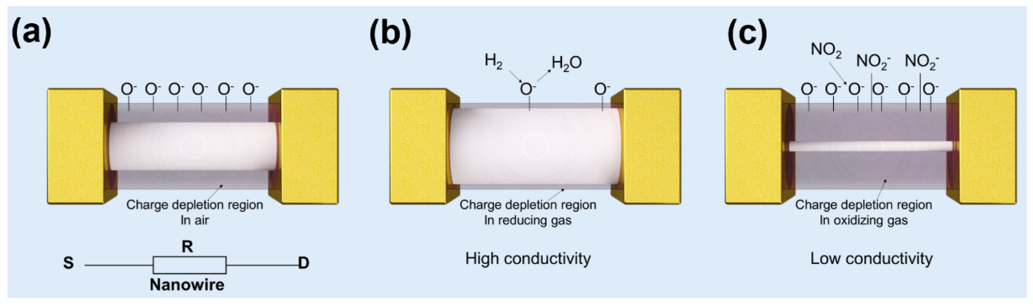
In a traditional chemiresistor sensor, Ohmic contact is highly preferred to study the intrinsic properties of nanowires. Generally, the classical D–L model is responsible for the sensitivity of nanowire gas sensors, where D represents nanowire diameter (D), and L represents the depth of the surface depletion layer (L) [342,343]. Considering the n-type oxide case, when a sensor is exposed to the atmosphere, oxygen can be adsorbed on the surface of metal–oxide nanowire and becomes negatively charged by the following equations [22]:
O2(gas) ↔ O2(ads)
O2(ads) + e− ↔ O2− (ads) (<100 °C)
O2−(ads) + e− ↔ 2O− (ads) (100–300 °C)
O−(ads) + e− ↔ O2− (ads) (>300 °C)
Such oxygen-charged behavior would extract electrons and create a shell-like surface depletion layer on the nanowire surface (Figure 22a), which can effectively modulate channel conductivity. Moreover, due to the adsorbed oxygen ions (O− and O2−), highly active towards reducing gas, high temperatures (>100 °C) are usually required to generate oxygen ions and enhance chemical reaction. For example, when the sensor is exposed to the gases (such as toluene, ethanol, CO, NH3, H2, methanol, shown in Equations (5)–(7) [22]), the charged oxygen (O−) can react with these gases, and release electrons back to the nanowire bulk. As a result, the thickness of the depletion layer is shrunk, leading to an increase in conductance (Figure 22b). In contrast, when the sensor is exposed to the oxidizing gases (such as NO2, O3, Equations (8) and (9) [22]), these gases can extract more electrons from the nanowire surface. Then, the depletion layer thickness increases and results in a reduction in nanowire conductance (Figure 22c):
CO(ads) + O−(ads) →CO2(gas)+ e−
CH3CH2OH(ads) + 6O−(ads) →2CO2(gas)+ 3H2O(gas)+ 6e−
H2(ads) + O−(ads) →H2O(gas)+ e−
e− + NO2(ads)↔ NO2−(ads)
2e− + O3(ads)↔ O2−(ads)+ O−(ads)
Due to its convenience in data analysis, tremendous works have used the Ohmic contacted device as a platform for fundamental studies to improve the device sensing performance.
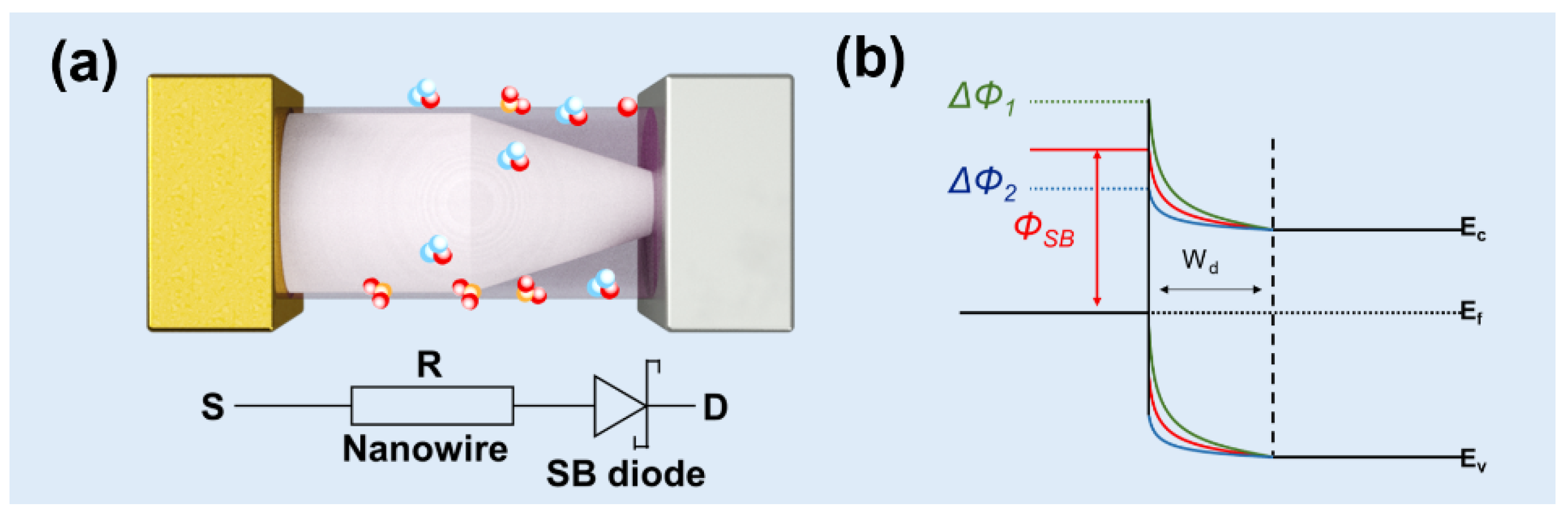
5.2. Schottky-Contacted Sensing
Recently, the Schottky-contacted nanowire sensors have attracted considerable attention due to the higher sensitivity, faster sensing response, shorter recovery time, and lower cost as compared with the conventional Ohmic-contacted nanowire sensors. In a typical Schottky-contacted sensor (Figure 23a), the overall resistance/conductance of the device is dominated by the Schottky barrier height (SBH), and its value is susceptible to external stimulus. Wei et al. firstly reported a Schottky-contacted nanowire sensor for gas molecules detection [344]. The device contains one Pt/ZnO junction (Schottky contact) and one Pt–Ga/ZnO junction (Ohmic contact). By comparing the sensing performance of the Schottky-contacted device and the conventional Ohmic-contacted device, it is shown that the Schottky-contacted sensor device presents 1085 times and 8776 times sensitivity improvement to oxidizing gas (O2) and reducing gas (CO), respectively. Furthermore, the Schottky contacted sensor device exhibited a faster response and shorter reset time, improved by a factor of 7. This new sensing concept has been extensively applied to other metal–oxide nanowire systems such as the well-known SnO2 [345] and In2O3 [346] nanowire-based sensors. Here, the author recommends the latest comprehensive review of Schottky-contacted nanowire sensors presented by Meng et al. [21].
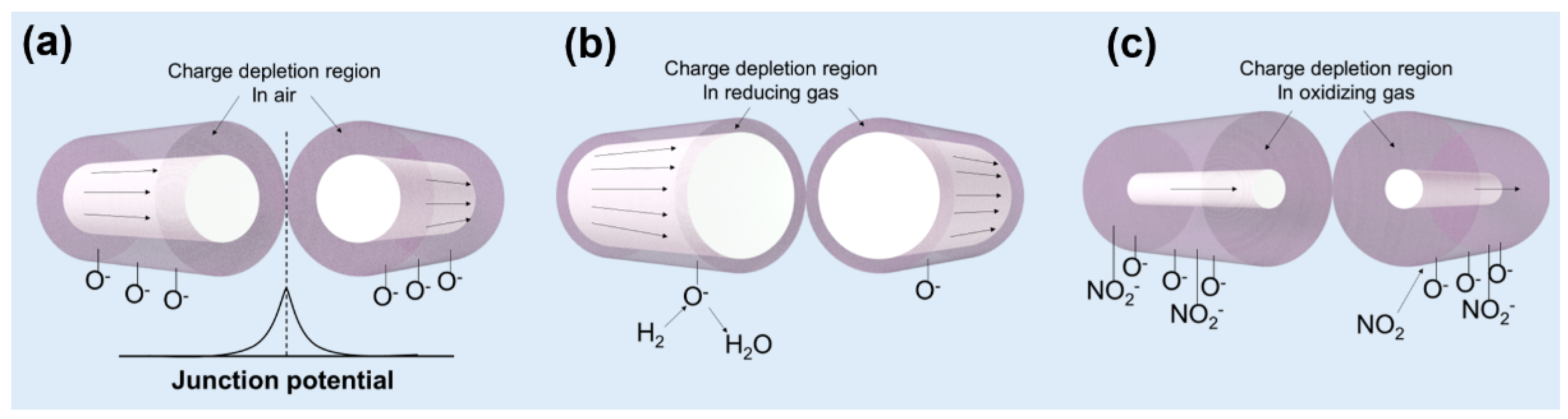
5.3. Nanowire–Nanowire Junctions Sensing
In the case of an n-type nanowire–nanowire junction sensor, as shown in Figure 24a, both the thickness of the electron depletion layer and the potential barrier height of the nanowire–nanowire interface dominates the overall conductance of the device. Furthermore, if the electron depletion layer is smaller than the nanowire diameter, the potential barrier heights of nanowire–nanowire junctions will play a crucial role in the gas sensing performance of nanowire sensors. Similar to the Schottky-contacted nanowire devices, the nanowire–nanowire barrier height can be decreased/increased when devices are exposed to a reducing/oxidizing atmosphere.
Many works have been performed using the interfacial sensing concept, not only for the simplicity in device fabrication but also for higher sensitivity. Most importantly, this concept also shows strong integration capability onto a sensing platform due to the development of nanowire devices with bridging structures [246]. Park et al. firstly reported a metal–oxide nanowire sensor with a bridging structure for NO2 detection [251]. As reported in their work, SnO2 nanowires are in situ grown at the pre-deposited electrode on-chip without using any arduous and individual lithography process. Due to self-connection with other nanowires, multiple nanowire–nanowire junctions are naturally formed as sensing channels. Consistent gas sensing characteristics can be seen due to the averaging effect of multi nanowire connections, and high sensitivity to NO2 is obtained (Rg/Ra = 230). Inspired by their encouraging work, other metal–oxide nanowires (ZnO, TiO2, and CuO) have also been applied to fabricate bridging structure sensors to combine the merits of in situ growth and nanowire–nanowire junctions sensing [177,191,250,263,347].
6. Critical Issues for Metal–Oxide Nanowire-Based Gas Sensor Devices
Despite all the extraordinary achievements of 1D nanowire-based sensors, some critical problems are still encouraged to be studied and investigated further to advance the nanowire sensor from the lab to the market. Here, we mainly discuss four critical issues: reproducibility, selectivity, stability, and energy consumption.
6.1. Reproducibility of Devices
Integrating a nanowire with contact electrodes on a platform allows us to study the intrinsic properties of the nanowire. However, a tiny variation in the size or shape of nanostructures will powerfully alter their physical and chemical properties. Thus, the nanowire-based electronics would inevitably suffer from poor reproducibility. To prevent the reproducibility issue, one easy method is to use a multiple nanowire sensor to eliminate the individual differences among nanowires. Currently, a commercially available fabrication process for the thin film sensor is used for the mat-like nanowire network sensor fabrication. Zhang et al. have compared the difference in electrical properties between single and multiple nanowire sensors [75]. It was found that all the multiple nanowire devices possess similar and consistent characteristics such as conductance, threshold gate voltage, and sensitivity to gas species. The fabrication of multiple nanowire gas sensors with the bridging structure is also an alternative approach to obtain molecular sensors with high uniformity [247]. The fabrication process in detail was described in Section 3.2.2. Unfortunately, those sensors did not really face/solve the reproducibility issues in the single nanowire devices. In fact, there is no difference between using multiple nanowire devices and conventional nanoparticle devices for gas sensing despite the porous structure.
6.2. Selectivity of Device
Another critical issue is the selectivity of the sensor device. Metal–oxide nanowire sensors generally have high sensitivity to the gas analytes, but they are also suffering from poor selectivity. To enhance the selectivity of sensors, a widely accepted method is introducing recognition elements on the sensing materials, for example, impurity elements doping, nanoparticle surface decorating, core/shell heterostructure construction. In addition, operational temperature modulation and nanowire architecture altering are also served as effective methods to improve the selectivity of the metal–oxide nanowire-based molecular sensors toward the target gas molecules. However, the results are usually far from prospects due to the low operational stability.
In addition, an alternative way to selectively detect the target gas molecules is to use the sensor array, because sensor arrays combined by a number of non-selective sensors which can acquire more information on a specific analyte than an individual sensor [348]. Subsequently, molecule information can be extracted from sensor arrays by appropriate pattern recognition techniques, such as principal component analysis (PCA) and back-propagation artificial neural network (BP-ANN) [349]. However, according to the research from Chen et al., multi-component sensing combined with PCA cannot work well if the reactions have no big difference between a specific target species and different metal–oxide surfaces [350]. Thus, enhancing the overall sensing performance of functional materials is the priority rather than data extraction and process. Unfortunately, this is usually not an easy task.
6.3. Long-Term Stability of the Device
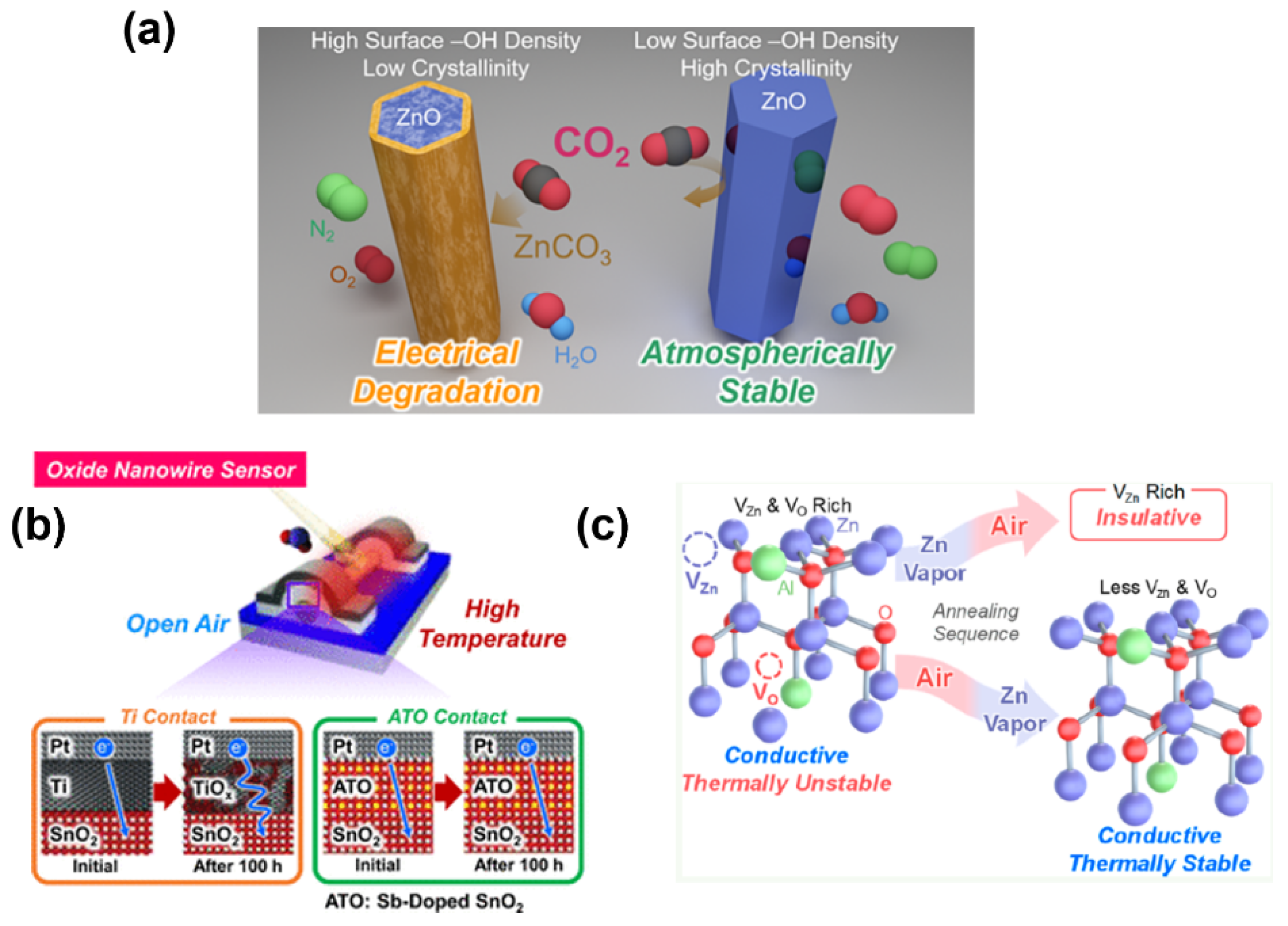
Stability, including chemical stability and physical stability, is the essential key to open the gate for sensor practical applications. Sysoev et al. firstly pointed out that using the nanowire network sensor can obtain long-term stable sensing performance compared with the conventional nanoparticle sensors because nanowires can prevent nanostructure aggregation [351]. However, although numerous efforts are devoted to improving the long-term stability of metal–oxide nanowire sensors, the influence of humidity, poisoning, and new contact issues still exist to prevent such a kind of sensors from the practical applications [47]. Steinhauer et al. reported that the sensing performance of CuO nanowire-based gas sensors is strongly weakened with the increase in surrounding H2O [47]. This is because the formation of the surface hydroxyl groups induced by H2O adsorption prevents the oxygen chemisorption from the surface active sites. Meanwhile, Nakamura et al. have noticed that a ppm-level CO2 in the air can react substantially with ZnO nanowire surfaces even at room temperature [74]. Such a reaction will form an electrically insulating zinc carbonate thin layer, which can critically determine the electrical stability of hydrothermally grown single-crystalline ZnO nanowires. In addition, Zeng et al. reported a contact issue in the conventional metal–oxide nanowire device [73]. Titanium has been most widely used to contact typical metal–oxide (e.g., SnO2, ZnO) by counting the energy level matching and good adhesion to the substrate, while the Ti contact can be oxidized easily, which causes an increase in contact resistance and further degradation in sensor performance after long-time operations under high temperature. Up to now, only a few papers have mentioned how to achieve long-term stability for metal–oxide nanowire sensors, and it is still remains a crucial challenge for commercialization.
6.4. Energy Consumption
An external heater is usually needed to elevate the temperature of metal–oxide gas sensors for effective gas sensing, which inevitably increases the power consumption and sensor size. There are currently two methods to solve this problem: (1) developing room temperature sensing materials; (2) using the self-Joule-heat technique. As for low-temperature sensors, tremendous progress has been made to reduce the operating temperature of the metal–oxide nanowire sensors, such as surface modification, additives doping, UV/visible-light irradiation. For example, Lupan et al. reported that the Pd-modified ZnO nanowires sensor could achieve room temperature sensing for H2. However, it appears to have other annoying troubles such as lower sensing response, longer response time, and slow recovery rate [352]. Self-Joule-heating is a nearly ideal strategy for operating nanowire gas sensors at ultralow power consumption, without additional heaters. Currently, it has been reported that conducting self-Joule-heat for nanowire sensors and remarkably decrease power consumption. Prades et al. have reported that the energy consumption of individual SnO2 nanowire sensor devices can be down to 20 μJ/s as self-Joule-heat is performed [218]. In addition, the power consumption of the nanowire sensor device could be further decreased via the pulsed self-heating technique [353]. However, recent studies on the self-Joule-heat technique only focused on controlling the spatial thermal properties of nanowires rather than tailoring the sensing performance of these sensors.
7. Prospective towards Metal–Oxide Nanowire Gas Sensor Electronics
As for the reproducibility of nanowire devices, we should carefully consider how to synthesize nanowires with high uniformity. Template-assisted nanowire growth is considered an alternative approach to achieve a highly ordered nanowire array. However, the complexity of template fabrication, low density of nanowires, and the extensive distribution of nanowire diameter have limited the wide application of such method [354]. Recently, Zhao et al. reported a two-step method to fabricate ZnO nanowires with uniformly shaped structures, as shown in Figure 25 [355]. Firstly, ZnO nanowires of random size are etched by NH4+ as the seed layer, and then, a very similar diameter (average about 17 nm with σ 1.3 nm, shown in Figure 25c) of ZnO nanowires are grown in the second step, which significantly increases the reproducibility of metal–oxide nanowire. This unique finding paves the way for the fabrication of nanowires-integrated nanodevices with reliable performance.
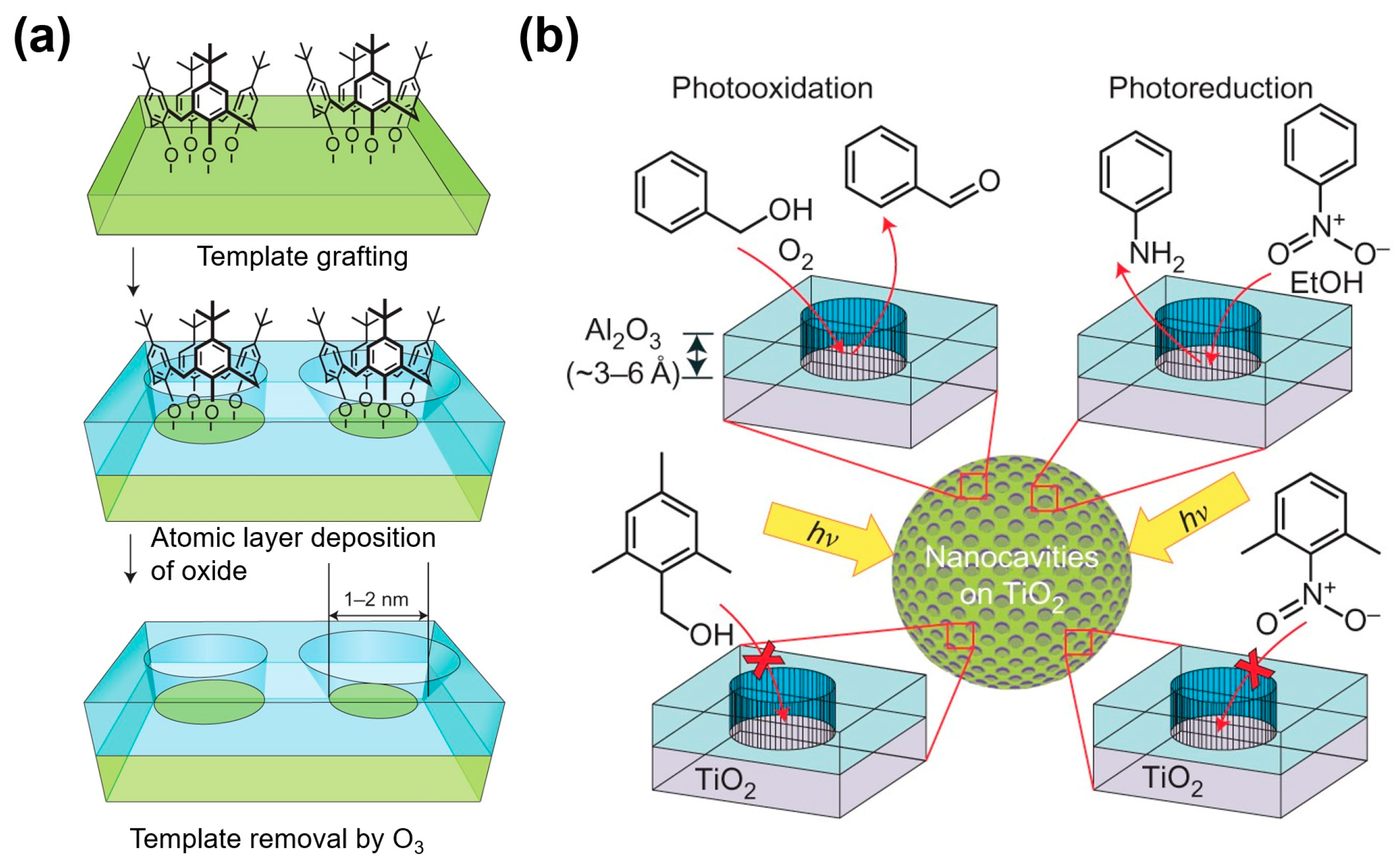
Poor selectivity is a perpetually perplexing problem that limits the wide application of the MOS gas sensor, including the metal–oxide nanowire-based sensors. Inspired by the catalytical chemistry, it is worth considering combining porous materials such as zeolites, metal–organic frameworks, and mesostructured oxides with a metal–oxide nanowire [356,357,358]. Canlas et al. reported a novel method to fabricate molecules imprinted oxide catalyst, and the fabrication process is shown in Figure 26 [359]. Using this structure, the nanocavities can preferentially react with nitrobenzene rather than nitroxylene in the photoreduction model and react with benzyl alcohol rather than 2,4,6-trimethylbenzyl alcohol in the photo-oxidation model. This technique can be applied to the metal–oxide nanowire sensor to gigantically improve selectivity due to their preferential interactions with specific VOC molecules, even with a chemically similar structure.
Solving the degradation issues, including nanowire degradation, contact degradation, and electrode degradation, is the only way to achieve long-term stability in nanowire devices. As shown in Figure 27a, Nakamura et al. demonstrated a strategy for achieving the atmospheric electrical stability of ZnO nanowires [74]. Via using a thermal annealing treatment in vacuum/air, the insulating layer induced by the unstable –OH layer on as fabricated ZnO nanowire surface is efficiently eliminated. Such a simple and low-cost method can enhance nanowire atmospheric stability for at least 40 days with stable electrical properties. Meanwhile, Zeng et al. offered a way to overcome the degradation in conventional sensor contact, as shown in Figure 27b [73]. It is found that the nanowire device can obtain good stability for at least over 2000 hours by replacing the easily oxidized contact metal (Ti) with heavily doped metal–oxide (antimony doped tin oxide). Moreover, Yan et al. reported an unusual annealing process on oxide thin films for highly thermal and chemical stability shown in Figure 27c [360,361]. It was indicated that Al-doped ZnO (AZO) nano-thin films could efficiently suppress the inevitable crystal defect formation in the as-fabricated thin film via sequential annealing process under air and Zn vapor atmosphere, resulting in a stable electrical resistivity (~10−4 Ω·cm) in air, even at high temperature (up to 500 °C). This thermally stable thin film can be utilized as electrodes for gas sensors, which obtain stable performance over 250 hours compared to the conventional Ti/Pt contact sensor. Meanwhile, the sequential annealed AZO nano-thin films also show highly chemical stability in buffer solution (pH: 3~11) compared with non-annealed AZO nano-thin films and ZnO thin films. These proposed strategies can successfully suppress the electrical performance degradation of the nanowire devices and have a great potential to be applied to various oxide nanostructures, which would give a foundation for the designing and fabrication of oxide nanomaterial-based IoT sensors with long-term stability.
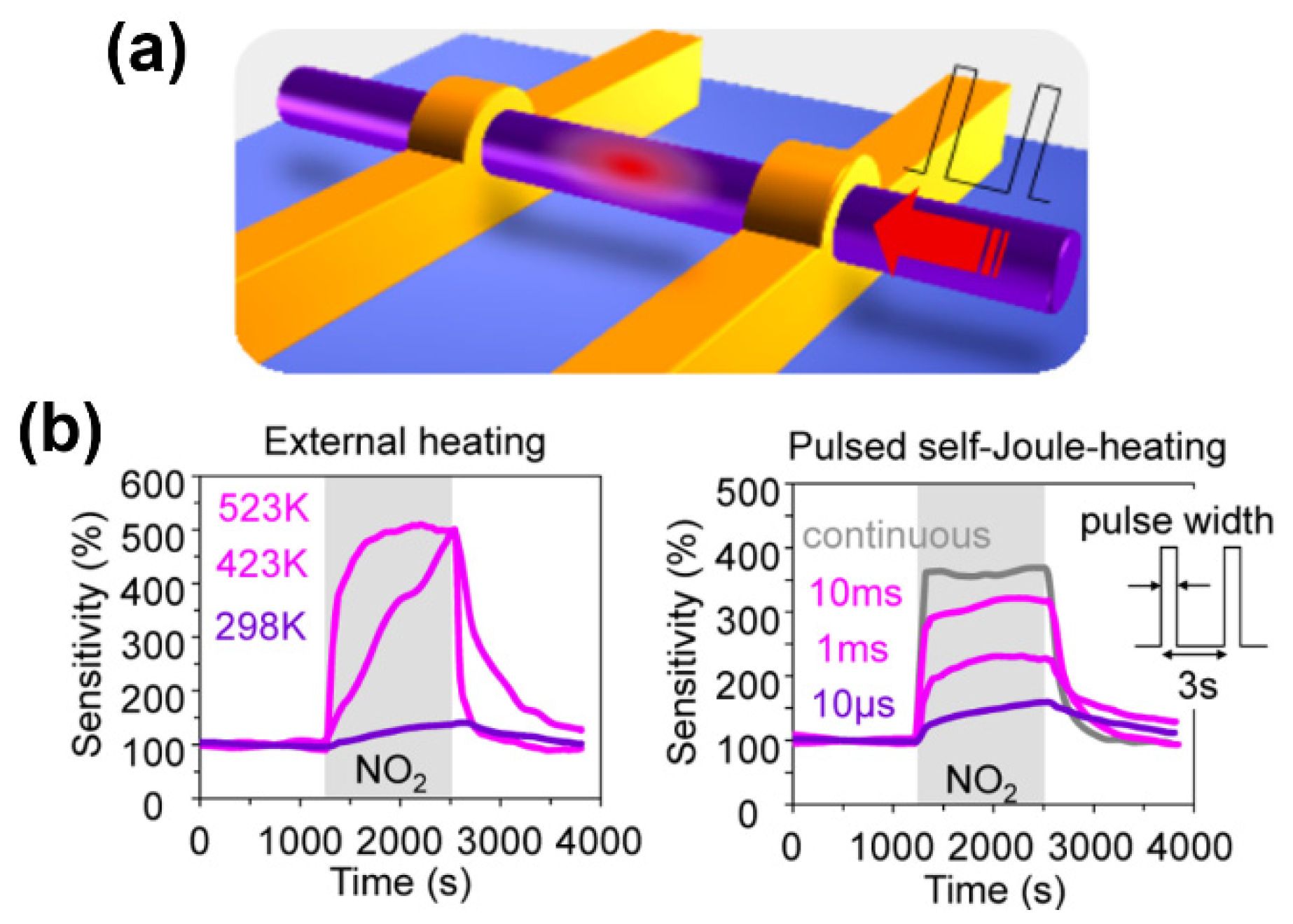
With regard to the low power consumption, Meng et al. recently reported an excellent thermal management approach in metal–oxide nanowire sensors via a pulsed self-Joule-heating technique, as shown in Figure 28 [220]. It was found that the thermal conductivity of the device was reduced due to the prohibition of heat dissipation from nanowire to surroundings, and its thermal relaxation times can be decreased down to a microsecond range, while several tens of seconds are needed for conventional MEMS gas sensors. This method enables the reduction in energy consumption down to ∼102 pJ/s and the enhancement of sensitivity for electrical sensing of NO2 (100 ppb). This proposed thermal management concept of nanowires in both spatial and time domains offers a strategy for exploring novel functionalities of nanowire-based sensors with high performance.
With the improvement of the metal–oxide nanowire synthesis and device fabrication processes with high uniformity, the integrated nanowire sensor electronics would have a high reproducibility, selectivity, and long-term stability. This would promote the nanowire sensor electronics to be widely used in the IoT applications, such as medicine, food industry, security, and environment protection.
Author Contributions
Writing—original draft preparation, H.Z.; writing—review and editing, G.Z., H.Z., K.N., T.T., T.H. and T.Y.; supervision, T.Y. All authors have read and agreed to the published version of the manuscript.
Funding
This research was funded by KAKENHI, grant number JP17H04927, JP18H01831, JP18H05243, and JP18KK0112. T.T. was supported by JST PRESTO Grant Number JPMJPR19M6, K.N. was supported by JST PRESTO Grant Number JPMJPR19J7, T.H. was supported by JST PRESTO Grant Number JPMJPR19T8, Japan. T.T., G.Z., K.N., and T.Y. were supported by JST CREST Grant Number JPMJCR19I2, Japan. T.Y. and K.N. were supported by CAS−JSPS Joint Research Projects (Grant Number JPJSBP120187207) and by Mirai R&D of JST.
Institutional Review Board Statement
Not applicable.
Informed Consent Statement
Not applicable.
Data Availability Statement
Data sharing not applicable.
Acknowledgments
This work was performed under the Cooperative Research Program of “Network Joint Research Center for Materials and Devices” and the MEXT Project of “Integrated Research Consortium on Chemical Sciences”.
Conflicts of Interest
The authors declare no conflict of interest.
References
- Lim, H.; Kim, H.S.; Qazi, R.; Kwon, Y.; Jeong, J.; Yeo, W. Wearable Flexible Hybrid Electronics: Advanced Soft Materials, Sensor Integrations, and Applications of Wearable Flexible Hybrid Electronics in Healthcare, Energy, and Environment. Adv. Mater. 2020, 32, 1–43. [Google Scholar]
- Güntner, A.T.; Abegg, S.; Königstein, K.; Gerber, P.A.; Schmidt-Trucksäss, A.; Pratsinis, S.E. Breath Sensors for Health Monitoring. ACS Sens. 2019, 4, 268–280. [Google Scholar] [CrossRef]
- Wang, T.; Ramnarayanan, A.; Cheng, H. Real Time Analysis of Bioanalytes in Healthcare, Food, Zoology and Botany. Sensors 2017, 18, 5. [Google Scholar] [CrossRef] [Green Version]
- Dincer, C.; Bruch, R.; Costa-Rama, E.; Fernández-Abedul, M.T.; Merkoçi, A.; Manz, A.; Urban, G.A.; Güder, F. Disposable Sensors in Diagnostics, Food, and Environmental Monitoring. Adv. Mater. 2019, 31, 1806739. [Google Scholar] [CrossRef]
- Fang, X.; Zong, B.; Mao, S. Metal–Organic Framework-Based Sensors for Environmental Contaminant Sensing. Nano-Micro Lett. 2018, 10, 1–19. [Google Scholar] [CrossRef] [Green Version]
- Wang, D.; Chen, A.; Jen, A.K.-Y. Reducing cross-sensitivity of TiO2-(B) nanowires to humidity using ultraviolet illumination for trace explosive detection. Phys. Chem. Chem. Phys. 2013, 15, 5017–5021. [Google Scholar] [CrossRef] [PubMed]
- Cao, A.; Zhu, W.; Shang, J.; Klootwijk, J.H.; Sudhölter, E.J.R.; Huskens, J.; De Smet, L.C.P.M. Metal–Organic Polyhedra-Coated Si Nanowires for the Sensitive Detection of Trace Explosives. Nano Lett. 2016, 17, 1–7. [Google Scholar] [CrossRef] [PubMed]
- Engel, Y.; Elnathan, R.; Pevzner, A.; Davidi, G.; Flaxer, E.; Patolsky, F. Supersensitive Detection of Explosives by Silicon Nanowire Arrays. Angew. Chem. Int. Ed. 2010, 49, 6830–6835. [Google Scholar] [CrossRef] [PubMed]
- Lan, A.; Li, K.; Wu, H.; Olson, D.H.; Emge, T.J.; Ki, W.; Hong, M.; Li, J. A Luminescent Microporous Metal-Organic Framework for the Fast And reversible Detection of High Explosives. Angew. Chem. Int. Ed. 2009, 48, 2334–2338. [Google Scholar] [CrossRef] [PubMed]
- Zappa, D. Low-Power Detection of Food Preservatives by a Novel Nanowire-Based Sensor Array. Foods 2019, 8, 226. [Google Scholar] [CrossRef] [PubMed] [Green Version]
- Carmona, E.N.; Sberveglieri, V.; Ponzoni, A.; Galstyan, V.; Zappa, D.; Pulvirenti, A.; Comini, E. Detection of food and skin pathogen microbiota by means of an electronic nose based on metal oxide chemiresistors. Sens. Actuators B Chem. 2017, 238, 1224–1230. [Google Scholar] [CrossRef]
- Mirzaei, A.; Lee, J.-H.; Majhi, S.M.; Weber, M.; Bechelany, M.; Kim, H.W.; Kim, S.S. Resistive gas sensors based on metal-oxide nanowires. J. Appl. Phys. 2019, 126, 241102. [Google Scholar] [CrossRef] [Green Version]
- Karnati, P.; Akbar, S.; Morris, P.A. Conduction mechanisms in one dimensional core-shell nanostructures for gas sensing: A review. Sens. Actuators B Chem. 2019, 295, 127–143. [Google Scholar] [CrossRef]
- Korotcenkov, G. Current Trends in Nanomaterials for Metal Oxide-Based Conductometric Gas Sensors: Advantages and Limitations. Part 1: 1D and 2D Nanostructures. Nanomaterials 2020, 10, 1392. [Google Scholar] [CrossRef] [PubMed]
- Majhi, S.M.; Mirzaei, A.; WooKimab, H.; Kim, S.S.; Kim, T.W. Recent advances in energy-saving chemiresistive gas sensors: A review. Nano Energy 2021, 79, 105369. [Google Scholar] [CrossRef]
- Joshi, N.; Hayasaka, T.; Liu, Y.; Liu, H.; Oliveira, O.N.; Lin, L. A review on chemiresistive room temperature gas sensors based on metal oxide nanostructures, graphene and 2D transition metal dichalcogenides. Microchim. Acta 2018, 185, 1–16. [Google Scholar] [CrossRef]
- Mounasamy, V.; Mani, G.K.; Madanagurusamy, S. Vanadium oxide nanostructures for chemiresistive gas and vapour sensing: A review on state of the art. Microchim. Acta 2020, 187, 1–29. [Google Scholar] [CrossRef]
- Wang, J.; Zhou, Q.; Peng, S.; Xu, L.; Zeng, W. Volatile Organic Compounds Gas Sensors Based on Molybdenum Oxides: A Mini Review. Front. Chem. 2020, 8, 1–7. [Google Scholar] [CrossRef]
- Comini, E. Metal oxides nanowires chemical/gas sensors: Recent advances. Mater. Today Adv. 2020, 7, 100099. [Google Scholar] [CrossRef]
- Wang, Y.; Duan, L.; Deng, Z.; Liao, J. Electrically Transduced Gas Sensors Based on Semiconducting Metal Oxide Nanowires. Sensors 2020, 20, 6781. [Google Scholar] [CrossRef]
- Meng, J.; Li, Z. Schottky-Contacted Nanowire Sensors. Adv. Mater. 2020, 32, 1–16. [Google Scholar] [CrossRef] [PubMed]
- Kaur, N.; Singh, M.; Comini, E. One-Dimensional Nanostructured Oxide Chemoresistive Sensors. Langmuir 2020, 36, 6326–6344. [Google Scholar] [CrossRef] [PubMed]
- Choi, P.G.; Izu, N.; Shirahata, N.; Masuda, Y. SnO2 Nanosheets for Selective Alkene Gas Sensing. ACS Appl. Nano Mater. 2019, 2, 1820–1827. [Google Scholar] [CrossRef]
- Miao, J.; Chen, C.; Meng, L.; Lin, J.Y. Self-Assembled Monolayer of Metal Oxide Nanosheet and Structure and Gas-Sensing Property Relationship. ACS Sens. 2019, 4, 1279–1290. [Google Scholar] [CrossRef]
- Kim, K.; Choi, P.G.; Itoh, T.; Masuda, Y. Catalyst-free Highly Sensitive SnO2 Nanosheet Gas Sensors for Parts per Billion-Level Detection of Acetone. ACS Appl. Mater. Interfaces 2020, 12, 51637–51644. [Google Scholar] [CrossRef]
- Govindhan, M.; Sidhureddy, B.; Chen, A. High-Temperature Hydrogen Gas Sensor Based on Three-Dimensional Hierarchical-Nanostructured Nickel–Cobalt Oxide. ACS Appl. Nano Mater. 2018, 1, 6005–6014. [Google Scholar] [CrossRef]
- Zhang, H.; Chen, W.-G.; Li, Y.-Q.; Song, Z.-H. Gas Sensing Performances of ZnO Hierarchical Structures for Detecting Dissolved Gases in Transformer Oil: A Mini Review. Front. Chem. 2018, 6, 1–7. [Google Scholar] [CrossRef]
- Li, N.; Fan, Y.; Shi, Y.; Xiang, Q.; Wang, X.; Xu, J. A low temperature formaldehyde gas sensor based on hierarchical SnO/SnO2 nano-flowers assembled from ultrathin nanosheets: Synthesis, sensing performance and mechanism. Sens. Actuators B Chem. 2019, 294, 106–115. [Google Scholar] [CrossRef]
- Kolmakov, A.; Zhang, Y.; Cheng, G.; Moskovits, M. Detection of CO and O2 Using Tin Oxide Nanowire Sensors. Adv. Mater. 2003, 15, 997–1000. [Google Scholar] [CrossRef]
- Huang, M.H.; Mao, S.; Feick, H.; Yan, H.Q.; Wu, Y.Y.; Kind, H.; Weber, E.; Russo, R.; Yang, P.D. Room-Temperature Ultraviolet Nanowire Nanolasers. Science 2001, 292, 1897–1899. [Google Scholar] [CrossRef] [PubMed] [Green Version]
- Li, J.Y.; Qiao, Z.Y.; Chen, X.L.; Chen, L.; Cao, Y.G.; He, M.; Li, H.; Cao, Z.M.; Zhang, Z. Synthesis of β-Ga2O3 Nanorods. J. Alloys Compd. 2000, 306, 300–302. [Google Scholar] [CrossRef]
- Comini, E.; Faglia, G.; Sberveglieri, G.; Pan, Z.; Wang, Z.L. Stable and highly sensitive gas sensors based on semiconducting oxide nanobelts. Appl. Phys. Lett. 2002, 81, 1869–1871. [Google Scholar] [CrossRef]
- Vomiero, A.; Bianchi, S.; Comini, E.; Faglia, G.; Ferroni, M.; Sberveglieri, G. Controlled Growth and Sensing Properties of In2O3 Nanowires. Cryst. Growth Des. 2007, 7, 2500–2504. [Google Scholar] [CrossRef]
- Lupan, O.; Postica, V.; Wolff, N.; Polonskyi, O.; Duppel, V.; Kaidas, V.; Lazari, E.; Ababii, N.; Faupel, F.; Kienle, L.; et al. Localized Synthesis of Iron Oxide Nanowires and Fabrication of High Performance Nanosensors Based on a Single Fe2O3 Nanowire. Small 2017, 13, 1–10. [Google Scholar]
- Jin, W.; Yan, S.; An, L.; Chen, W.; Yang, S.; Zhao, C.; Dai, Y. Enhancement of ethanol gas sensing response based on ordered V2O5 nanowire microyarns. Sens. Actuators B Chem. 2015, 206, 284–290. [Google Scholar] [CrossRef]
- Fu, X.Q.; Wang, C.; Yu, H.C.; Wang, Y.G.; Wang, T.H. Fast humidity sensors based on CeO2 nanowires. Nanotechnology 2007, 18, 145503. [Google Scholar] [CrossRef]
- Baratto, C.; Kumar, R.; Comini, E.; Faglia, G.; Sberveglieri, G. Gas Sensing Study of ZnO Nanowire Heterostructured with NiO for Detection of Pollutant Gases. Procedia Eng. 2014, 87, 1091–1094. [Google Scholar] [CrossRef] [Green Version]
- Kaur, N.; Zappa, D.; Poli, N.; Comini, E. Integration of VLS-Grown WO3 Nanowires into Sensing Devices for the Detection of H2S and O3. ACS Omega 2019, 4, 16336–16343. [Google Scholar] [CrossRef] [Green Version]
- Kaur, N.; Comini, E.; Zappa, D.; Poli, N.; Sberveglieri, G. Nickel oxide nanowires: Vapor liquid solid synthesis and integration into a gas sensing device. Nanotechnology 2016, 27, 205701. [Google Scholar] [CrossRef]
- Lupan, O.; Cretu, V.; Postica, V.; Ahmadi, M.; Cuenya, B.R.; Chow, L.; Tiginyanu, I.; Viana, B.; Pauporté, T.; Adelung, R. Silver-Doped Zinc Oxide Single Nanowire Multifunctional Nanosensor with a Significant Enhancement in Response. Sens. Actuators B Chem. 2016, 223, 893–903. [Google Scholar] [CrossRef]
- Gu, L.; Zhou, D.; Cao, J.C. Piezoelectric Active Humidity Sensors Based on Lead-Free NaNbO3 Piezoelectric Nanofibers. Sensors 2016, 16, 833. [Google Scholar] [CrossRef] [Green Version]
- Zhou, T.; Liu, X.; Zhang, R.; Wang, Y.; Zhang, T. Shape control and selective decoration of Zn2SnO4 nanostructures on 1D nanowires: Boosting chemical–sensing performances. Sens. Actuators B Chem. 2019, 290, 210–216. [Google Scholar] [CrossRef]
- Thanh, H.X.; Trung, D.D.; Trung, K.Q.; Van Dam, K.; Van Duy, N.; Hung, C.M.; Hoa, N.D.; Van Hieu, N. On-chip growth of single phase Zn2SnO4 nanowires by thermal evaporation method for gas sensor application. J. Alloys Compd. 2017, 708, 470–475. [Google Scholar] [CrossRef]
- Cheng, Z.; Huang, C.; Song, L.; Wang, Y.; Ding, Y.; Xu, J.; Zhang, Y. Electrospinning synthesis of CdIn2O4 nanofibers for ethanol detection. Sens. Actuators B Chem. 2015, 209, 530–535. [Google Scholar] [CrossRef]
- Gu, G.; Zheng, B.; Han, W.Q.; Roth, S.; Liu, J. Tungsten Oxide Nanowires on Tungsten Substrates. Nano Lett. 2002, 2, 849–851. [Google Scholar] [CrossRef]
- Baek, D.-H.; Choi, J.; Kim, J. Fabrication of suspended nanowires for highly sensitive gas sensing. Sens. Actuators B Chem. 2019, 284, 362–368. [Google Scholar] [CrossRef]
- Steinhauer, S.; Chapelle, A.; Menini, P.; Sowwan, M. Local CuO Nanowire Growth on Microhotplates: In Situ Electrical Measurements and Gas Sensing Application. ACS Sens. 2016, 1, 503–507. [Google Scholar] [CrossRef]
- Chen, J.; Wang, K.; Zhou, W. Vertically Aligned ZnO Nanorod Arrays Coated with SnO2/Noble Metal Nanoparticles for Highly Sensitive and Selective Gas Detection. IEEE Trans. Nanotechnol. 2010, 10, 968–974. [Google Scholar] [CrossRef]
- Ford, A.C.; Ho, J.C.; Chueh, Y.-L.; Tseng, Y.-C.; Fan, Z.; Guo, J.; Bokor, J.; Javey, A. Diameter-Dependent Electron Mobility of InAs Nanowires. Nano Lett. 2009, 9, 360–365. [Google Scholar] [CrossRef]
- Duan, J.-L.; Liu, J.; Yao, H.-J.; Mo, D.; Hou, M.-D.; Sun, Y.-M.; Chen, Y.-F.; Zhang, L. Controlled synthesis and diameter-dependent optical properties of Cu nanowire arrays. Mater. Sci. Eng. B 2008, 147, 57–62. [Google Scholar] [CrossRef]
- Li, D.; Wu, Y.; Kim, P.; Shi, L.; Yang, P.; Majumdar, A. Thermal conductivity of individual silicon nanowires. Appl. Phys. Lett. 2003, 83, 2934–2936. [Google Scholar] [CrossRef]
- Tonezzer, M.; Hieu, N. Size-dependent response of single-nanowire gas sensors. Sens. Actuators B Chem. 2012, 163, 146–152. [Google Scholar] [CrossRef]
- Xia, Y.; Yang, P.; Sun, Y.; Wu, Y.; Mayers, B.; Gates, B.; Yin, Y.; Kim, F.; Yan, H. One-Dimensional Nanostructures: Synthesis, Characterization, and Applications. Adv. Mater. 2003, 15, 353–389. [Google Scholar] [CrossRef]
- Gröttrup, J.; Postica, V.; Ababii, N.; Lupan, O.; Zamponi, C.; Meyners, D.; Mishra, Y.K.; Sontea, V.; Tiginyanu, I.; Adelung, R. Size-Dependent UV and Gas Sensing Response of Individual Fe2O3-ZnO:Fe Micro- and Nanowire Based Devices. J. Alloys Compd. 2017, 701, 920–925. [Google Scholar] [CrossRef]
- Kim, K.; Kwak, H.-T.; Cho, H.; Meyyappan, M.; Baek, C.-K. Design Guidelines for High Sensitivity ZnO Nanowire Gas Sensors with Schottky Contact. IEEE Sens. J. 2019, 19, 976–981. [Google Scholar] [CrossRef]
- Walker, J.M.; Akbar, S.A.; Morris, P.A. Synergistic effects in gas sensing semiconducting oxide nano-heterostructures: A review. Sens. Actuators B Chem. 2019, 286, 624–640. [Google Scholar] [CrossRef]
- Zappa, D.; Galstyan, V.; Kaur, N.; Munasinghe Arachchige, H.M.M.; Sisman, O.; Comini, E. “Metal Oxide -Based Heterostructures for Gas Sensors”- A Review. Anal. Chim. Acta 2018, 1039, 1–23. [Google Scholar] [CrossRef]
- Simakov, V.; Sinev, I.; Shikunov, D.; Tymoshenko, D.; Smirnov, A.; Zaitsev, B. Experimental investigation and modeling of temperature influence on vertical and radial growth rate of tin dioxide nanowires synthesized by catalyst-free thermal evaporation method. Mater. Chem. Phys. 2020, 242, 122502. [Google Scholar] [CrossRef]
- Singh, N.; Ponzoni, A.; Comini, E.; Lee, P.S. Chemical sensing investigations on Zn–In2O3 nanowires. Sens. Actuators B Chem. 2012, 171, 244–248. [Google Scholar] [CrossRef]
- Liu, Z.; Zhang, D.; Han, S.; Li, C.; Tang, T.; Jin, W.; Liu, X.; Lei, B.; Zhou, C. Laser Ablation Synthesis and Electron Transport Studies of Tin Oxide Nanowires. Adv. Mater. 2003, 15, 1754–1757. [Google Scholar] [CrossRef]
- Shkurmanov, A.; Sturm, C.; Franke, H.; Lenzner, J.; Grundmann, M. Low-Temperature PLD-Growth of Ultrathin ZnO Nanowires by Using ZnxAl1−xO and ZnxGa1−xO Seed Layers. Nanoscale Res. Lett. 2017, 12, 1–7. [Google Scholar] [CrossRef] [Green Version]
- Liang, J.; Zhao, Y.; Zhu, K.; Guo, J.; Zhou, L. Synthesis and room temperature NO2 gas sensitivity of vanadium dioxide nanowire structures by chemical vapor deposition. Thin Solid Films 2019, 669, 537–543. [Google Scholar] [CrossRef]
- Vallejos, S.; Gràcia, I.; Lednický, T.; Vojkuvka, L.; Figueras, E.; Hubálek, J.; Cané, C. Highly Hydrogen Sensitive Micromachined Sensors Based on Aerosol-Assisted Chemical Vapor Deposited ZnO Rods. Sens. Actuators B Chem. 2018, 268, 15–21. [Google Scholar] [CrossRef]
- Nekita, S.; Nagashima, K.; Zhang, G.; Wang, Q.; Kanai, M.; Takahashi, T.; Hosomi, T.; Nakamura, K.; Okuyama, T.; Yanagida, T. Face-Selective Crystal Growth of Hydrothermal Tungsten Oxide Nanowires for Sensing Volatile Molecules. ACS Appl. Nano Mater. 2020, 3, 10252–10260. [Google Scholar] [CrossRef]
- Liu, Q.; Yasui, T.; Nagashima, K.; Yanagida, T.; Hara, M.; Horiuchi, M.; Zhu, Z.; Takahashi, H.; Shimada, T.; Arima, A.; et al. Ammonia-Induced Seed Layer Transformations in a Hydrothermal Growth Process of Zinc Oxide Nanowires. J. Phys. Chem. C 2020, 124, 20563–20568. [Google Scholar] [CrossRef]
- Wang, Q.; Huang, J.; Zhou, J.; Liu, Z.; Geng, Y.; Liang, Z.; Du, Y.; Tian, X. Different nanostructured tungsten oxides synthesized by facile solvothermal route for chlorine gas sensing. Sens. Actuators B Chem. 2018, 275, 306–311. [Google Scholar] [CrossRef]
- Qin, Y.; Li, X.; Wang, F.; Hu, M. Solvothermally synthesized tungsten oxide nanowires/nanorods for NO2 gas sensor applications. J. Alloys Compd. 2011, 509, 8401–8406. [Google Scholar] [CrossRef]
- Dasgupta, N.P.; Sun, J.; Liu, C.; Brittman, S.; Andrews, S.C.; Lim, J.; Gao, H.; Yan, R.; Yang, P. 25th Anniversary Article: Semiconductor Nanowires-Synthesis, Characterization, and Applications. Adv. Mater. 2014, 26, 2137–2184. [Google Scholar] [CrossRef] [PubMed]
- Asadzadeh, M.Z.; Köck, A.; Popov, M.; Steinhauer, S.; Spitaler, J.; Romaner, L. Response modeling of single SnO2 nanowire gas sensors. Sens. Actuators B Chem. 2019, 295, 22–29. [Google Scholar] [CrossRef]
- Gall, O.Z.; Zhong, X.; Schulman, D.S.; Kang, M.; Razavieh, A.; Mayer, T.S. Titanium dioxide nanowire sensor array integration on CMOS platform using deterministic assembly. Nanotechnology 2017, 28, 265501. [Google Scholar] [CrossRef] [PubMed]
- Jeong, S.; Kim, J.; Lee, J. Rational Design of Semiconductor-Based Chemiresistors and their Libraries for Next-Generation Artificial Olfaction. Adv. Mater. 2020, 32, 1–47. [Google Scholar] [CrossRef]
- Zhou, Z.; Lan, C.; Wei, R.; Ho, J.C. Transparent metal-oxide nanowires and their applications in harsh electronics. J. Mater. Chem. C 2018, 7, 202–217. [Google Scholar] [CrossRef]
- Zeng, H.; Takahashi, T.; Kanai, M.; Zhang, G.; He, Y.; Nagashima, K.; Yanagida, T. Long-Term Stability of Oxide Nanowire Sensors via Heavily Doped Oxide Contact. ACS Sens. 2017, 2, 1854–1859. [Google Scholar] [CrossRef]
- Nakamura, K.; Takahashi, T.; Hosomi, T.; Seki, T.; Kanai, M.; Zhang, G.; Nagashima, K.; Shibata, N.; Yanagida, T. Redox-Inactive CO2 Determines Atmospheric Stability of Electrical Properties of ZnO Nanowire Devices through a Room-Temperature Surface Reaction. ACS Appl. Mater. Interfaces 2019, 11, 40260–40266. [Google Scholar] [CrossRef]
- Zhang, D.; Liu, Z.; Li, C.; Tang, T.; Liu, X.; Han, S.; Lei, A.B.; Zhou, C. Detection of NO2 down to ppb Levels Using Individual and Multiple In2O3 Nanowire Devices. Nano Lett. 2004, 4, 1919–1924. [Google Scholar] [CrossRef]
- Verma, V.P.; Das, S.; Hwang, S.; Choi, H.; Jeon, M.; Choi, W. Nitric oxide gas sensing at room temperature by functionalized single zinc oxide nanowire. Mater. Sci. Eng. B 2010, 171, 45–49. [Google Scholar] [CrossRef]
- Johnson, M.C.; Aloni, S.; McCready, D.E.; Bourret-Courchesne, E.D. Controlled Vapor−Liquid−Solid Growth of Indium, Gallium, and Tin Oxide Nanowires via Chemical Vapor Transport. Cryst. Growth Des. 2006, 6, 1936–1941. [Google Scholar] [CrossRef]
- Anzai, H.; Suzuki, M.; Nagashima, K.; Kanai, M.; Guozhu, Z.; He, Y.; Boudot, M.; Zhang, G.; Takahashi, T.; Kanemoto, K.; et al. True Vapor–Liquid–Solid Process Suppresses Unintentional Carrier Doping of Single Crystalline Metal Oxide Nanowires. Nano Lett. 2017, 17, 4698–4705. [Google Scholar] [CrossRef] [PubMed]
- Bang, J.H.; Choi, M.S.; Mirzaei, A.; Kwon, Y.J.; Kim, S.S.; Kim, T.W.; Kim, H.W. Selective NO2 sensor based on Bi2O3 branched SnO2 nanowires. Sens. Actuators B Chem. 2018, 274, 356–369. [Google Scholar] [CrossRef]
- Kim, J.-H.; Mirzaei, A.; Kim, J.-Y.; Lee, J.-H.; Kim, H.W.; Hishita, S.; Kim, S.S. Enhancement of gas sensing by implantation of Sb-ions in SnO2 nanowires. Sens. Actuators B Chem. 2020, 304, 127307. [Google Scholar] [CrossRef]
- Morales, A.M.; Lieber, C.M. A Laser Ablation Method for the Synthesis of Crystalline Semiconductor Nanowires. Science 1998, 279, 208–211. [Google Scholar] [CrossRef]
- Zervos, M.; Mihailescu, C.N.; Giapintzakis, J.; Luculescu, C.R.; Florini, N.; Komninou, P.; Kioseoglou, J.; Othonos, A. Broad compositional tunability of indium tin oxide nanowires grown by the vapor-liquid-solid mechanism. APL Mater. 2014, 2, 056104. [Google Scholar] [CrossRef]
- Zhu, Z.; Suzuki, M.; Nagashima, K.; Yoshida, H.; Kanai, M.; Meng, G.; Anzai, H.; Zhuge, F.; He, Y.; Boudot, M.; et al. Rational Concept for Reducing Growth Temperature in Vapor–Liquid–Solid Process of Metal Oxide Nanowires. Nano Lett. 2016, 16, 7495–7502. [Google Scholar] [CrossRef] [PubMed]
- Meng, G.; Yanagida, T.; Nagashima, K.; Yoshida, H.; Kanai, M.; Klamchuen, A.; Zhuge, F.; He, Y.; Rahong, S.; Fang, X.; et al. Impact of Preferential Indium Nucleation on Electrical Conductivity of Vapor–Liquid–Solid Grown Indium–Tin Oxide Nanowires. J. Am. Chem. Soc. 2013, 135, 7033–7038. [Google Scholar] [CrossRef] [PubMed]
- Klamchuen, A.; Suzuki, M.; Nagashima, K.; Yoshida, H.; Kanai, M.; Zhuge, F.; He, Y.; Meng, G.; Kai, S.; Takeda, S.; et al. Rational Concept for Designing Vapor–Liquid–Solid Growth of Single Crystalline Metal Oxide Nanowires. Nano Lett. 2015, 15, 6406–6412. [Google Scholar] [CrossRef] [PubMed]
- Meng, G.; Yanagida, T.; Yoshida, H.; Nagashima, K.; Kanai, M.; Zhuge, F.; He, Y.; Klamchuen, A.; Rahong, S.; Fang, X.; et al. A flux induced crystal phase transition in the vapor–liquid–solid growth of indium-tin oxide nanowires. Nanoscale 2014, 6, 7033–7038. [Google Scholar] [CrossRef]
- Jeongseok, L.; Se-Hyeong, L.; So-Young, B.; Yoojong, K.; Kyoungwan, W.; Sanghyun, L.; Yooseong, L.; Moonsuk, Y. Improved Sensitivity of α-Fe2O3 Nanoparticle-Decorated ZnO Nanowire Gas Sensor for CO. Sensors 2019, 19, 1903. [Google Scholar]
- Kim, J.-H.; Mirzaei, A.; Kim, H.W.; Kim, S.S. Improving the hydrogen sensing properties of SnO2 nanowire-based conductometric sensors by Pd-decoration. Sens. Actuators B Chem. 2019, 285, 358–367. [Google Scholar] [CrossRef]
- Woo, H.-S.; Kwak, C.-H.; Chung, J.-H.; Lee, J.-H. Highly selective and sensitive xylene sensors using Ni-doped branched ZnO nanowire networks. Sens. Actuators B Chem. 2015, 216, 358–366. [Google Scholar] [CrossRef]
- Afshar, M.; Preiß, E.M.; Sauerwald, T.; Rodner, M.; FeiLi, D.; Straub, M.; König, K.; Schütze, A.; Seidel, H.; Preiss, E. Indium-tin-oxide single-nanowire gas sensor fabricated via laser writing and subsequent etching. Sens. Actuators B Chem. 2015, 215, 525–535. [Google Scholar] [CrossRef]
- Nguyen, P.; Ng, H.T.; Kong, J.; Cassell, A.M.; Quinn, R.; Li, J.; Han, J.; McNeil, M.; Meyyappan, M. Epitaxial Directional Growth of Indium-Doped Tin Oxide Nanowire Arrays. Nano Lett. 2003, 3, 925–928. [Google Scholar] [CrossRef]
- Xue, X.Y.; Chen, Y.J.; Liu, Y.G.; Shi, S.L.; Wang, Y.G.; Wang, T.H. Synthesis and ethanol sensing properties of indium-doped tin oxide nanowires. Appl. Phys. Lett. 2006, 88, 201907. [Google Scholar] [CrossRef]
- Kaur, N.; Comini, E.; Poli, N.; Zappa, D.; Sberveglieri, G. Nickel Oxide Nanowires Growth by VLS Technique for Gas Sensing Application. Procedia Eng. 2015, 120, 760–763. [Google Scholar] [CrossRef]
- Nagashima, K.; Yoshida, H.; Klamchuen, A.; Kanai, M.; Meng, G.; Zhuge, F.; He, Y.; Anzai, H.; Zhu, Z.; Suzuki, M.; et al. Tailoring Nucleation at Two Interfaces Enables Single Crystalline NiO Nanowires via Vapor–Liquid–Solid Route. ACS Appl. Mater. Interfaces 2016, 8, 27892–27899. [Google Scholar] [CrossRef] [PubMed]
- Oka, K.; Yanagida, T.; Nagashima, K.; Kawai, T.; Kim, J.-S.; Park, B.H. Resistive-Switching Memory Effects of NiO Nanowire/Metal Junctions. J. Am. Chem. Soc. 2010, 132, 6634–6635. [Google Scholar] [CrossRef] [PubMed]
- Chang, P.-C.; Fan, Z.; Wang, D.; Tseng, W.-Y.; Chiou, W.-A.; Hong, J.; Lu, J.G. ZnO Nanowires Synthesized by Vapor Trapping CVD Method. Chem. Mater. 2004, 16, 5133–5137. [Google Scholar] [CrossRef]
- Kuang, Q.; Lao, C.; Wang, Z.L.; Xie, Z.; Zheng, L. High-Sensitivity Humidity Sensor Based on a Single SnO2 Nanowire. J. Am. Chem. Soc. 2007, 129, 6070–6071. [Google Scholar] [CrossRef] [Green Version]
- Klamchuen, A.; Yanagida, T.; Kanai, M.; Nagashima, K.; Oka, K.; Seki, S.; Suzuki, M.; Hidaka, Y.; Kai, S.; Kawai, T. Dopant homogeneity and transport properties of impurity-doped oxide nanowires. Appl. Phys. Lett. 2011, 98, 053107. [Google Scholar] [CrossRef]
- Zhuge, F.; Yanagida, T.; Nagashima, K.; Yoshida, H.; Kanai, M.; Xu, B.; Klamchuen, A.; Meng, G.; He, Y.; Rahong, S.; et al. Fundamental Strategy for Creating VLS Grown TiO2 Single Crystalline Nanowires. J. Phys. Chem. C 2012, 116, 24367–24372. [Google Scholar] [CrossRef]
- Kim, M.H.; Baik, J.M.; Zhang, J.; Larson, C.; Li, Y.; Stucky, G.D.; Moskovits, M.; Wodtke, A.M. TiO2 Nanowire Growth Driven by Phosphorus-Doped Nanocatalysis. J. Phys. Chem. C 2010, 114, 10697–10702. [Google Scholar] [CrossRef]
- Li, C.; Zhang, D.; Han, S.; Liu, X.; Tang, T.; Zhou, C. Diameter-Controlled Growth of Single-Crystalline In2O3 Nanowires and Their Electronic Properties. Adv. Mater. 2003, 15, 143–146. [Google Scholar] [CrossRef]
- Liang, C.H.; Meng, G.W.; Lei, Y.; Phillipp, F.; Zhang, L.D. Catalytic Growth of Semiconducting In2O3 Nanofibers. Adv. Mater. 2001, 13, 1330–1333. [Google Scholar] [CrossRef]
- Dang, H.Y.; Wang, J.; Fan, S.S. The synthesis of metal oxide nanowires by directly heating metal samples in appropriate oxygen atmospheres. Nanotechnology 2003, 14, 738–741. [Google Scholar] [CrossRef]
- Yan, Y.; Zhou, L.; Zhang, J.; Zeng, H.; Zhang, Y.; Zhang, L. Synthesis and Growth Discussion of One-Dimensional MgO Nanostructures: Nanowires, Nanobelts, and Nanotubes in VLS Mechanism. J. Phys. Chem. C 2008, 112, 10412–10417. [Google Scholar] [CrossRef]
- Yanagida, T.; Nagashima, K.; Tanaka, H.; Kawai, T. Mechanism of critical catalyst size effect on MgO nanowire growth by pulsed laser deposition. J. Appl. Phys. 2008, 104, 016101. [Google Scholar] [CrossRef] [Green Version]
- A Fortuna, S.; Li, X. Metal-catalyzed semiconductor nanowires: A review on the control of growth directions. Semicond. Sci. Technol. 2010, 25, 024005. [Google Scholar] [CrossRef] [Green Version]
- Weng, T.-F.; Ho, M.-S.; Sivakumar, C.; Balraj, B.; Chung, P.-F. VLS growth of pure and Au decorated β-Ga2O3 nanowires for room temperature CO gas sensor and resistive memory applications. Appl. Surf. Sci. 2020, 533, 147476. [Google Scholar] [CrossRef]
- Klamchuen, A.; Yanagida, T.; Nagashima, K.; Seki, S.; Oka, K.; Taniguchi, M.; Kawai, T. Crucial Role of Doping Dynamics on Transport Properties of Sb-Doped SnO2 Nanowires. Appl. Phys. Lett. 2009, 95, 7–9. [Google Scholar] [CrossRef] [Green Version]
- Marcu, A.; Yanagida, T.; Nagashima, K.; Oka, K.; Tanaka, H.; Kawai, T. Crucial Role of Interdiffusion on Magnetic Properties of in Situ Formed MgO Fe3-ΔO4 Heterostructured Nanowires. Appl. Phys. Lett. 2008, 92, 3–5. [Google Scholar] [CrossRef]
- Marcu, A.; Yanagida, T.; Nagashima, K.; Tanaka, H.; Kawai, T. Effect of ablated particle flux on MgO nanowire growth by pulsed laser deposition. J. Appl. Phys. 2007, 102, 016102. [Google Scholar] [CrossRef]
- He, Y.; Yanagida, T.; Nagashima, K.; Zhuge, F.; Meng, G.; Xu, B.; Klamchuen, A.; Rahong, S.; Kanai, M.; Li, X.; et al. Crystal-Plane Dependence of Critical Concentration for Nucleation on Hydrothermal ZnO Nanowires. J. Phys. Chem. C 2013, 117, 1197–1203. [Google Scholar] [CrossRef]
- Nagashima, K.; Yanagida, T.; Kanai, M.; Oka, K.; Klamchuen, A.; Rahong, S.; Meng, G.; Horprathum, M.; Xu, B.; Zhuge, F.; et al. Switching Properties of Titanium Dioxide Nanowire Memristor. Jpn. J. Appl. Phys. 2012, 51, 9–12. [Google Scholar] [CrossRef] [Green Version]
- Nagashima, K.; Yanagida, T.; Klamchuen, A.; Kanai, M.; Oka, K.; Seki, S.; Kawai, T.; Lee, Y.-H.; Lee, J.-H. Interfacial effect on metal/oxide nanowire junctions. Appl. Phys. Lett. 2010, 96, 073110. [Google Scholar] [CrossRef]
- Nagashima, K.; Yanagida, T.; Oka, K.; Kanai, M.; Klamchuen, A.; Kim, J.-S.; Park, B.H.; Kawai, T. Intrinsic Mechanisms of Memristive Switching. Nano Lett. 2011, 11, 2114–2118. [Google Scholar] [CrossRef]
- Nagashima, K.; Yanagida, T.; Oka, K.; Kanai, M.; Klamchuen, A.; Rahong, S.; Meng, G.; Horprathum, M.; Xu, B.; Zhuge, F.; et al. Prominent Thermodynamical Interaction with Surroundings on Nanoscale Memristive Switching of Metal Oxides. Nano Lett. 2012, 12, 5684–5690. [Google Scholar] [CrossRef]
- Nagashima, K.; Yanagida, T.; Oka, K.; Tanaka, H.; Kawai, T. Mechanism and control of sidewall growth and catalyst diffusion on oxide nanowire vapor-liquid-solid growth. Appl. Phys. Lett. 2008, 93, 153103. [Google Scholar] [CrossRef]
- Nagashima, K.; Yanagida, T.; Oka, K.; Taniguchi, M.; Kawai, T.; Kim, J.-S.; Park, B.H. Resistive Switching Multistate Nonvolatile Memory Effects in a Single Cobalt Oxide Nanowire. Nano Lett. 2010, 10, 1359–1363. [Google Scholar] [CrossRef]
- Nagashima, K.; Yanagida, T.; Tanaka, H.; Kawai, T. Control of magnesium oxide nanowire morphologies by ambient temperature. Appl. Phys. Lett. 2007, 90, 233103. [Google Scholar] [CrossRef] [Green Version]
- Nagashima, K.; Yanagida, T.; Tanaka, H.; Kawai, T. Epitaxial growth of MgO nanowires by pulsed laser deposition. J. Appl. Phys. 2007, 101, 124304. [Google Scholar] [CrossRef] [Green Version]
- Oka, K.; Yanagida, T.; Nagashima, K.; Kanai, M.; Kawai, T.; Kim, J.-S.; Park, B.H. Spatial Nonuniformity in Resistive-Switching Memory Effects of NiO. J. Am. Chem. Soc. 2011, 133, 12482–12485. [Google Scholar] [CrossRef]
- Oka, K.; Yanagida, T.; Nagashima, K.; Kanai, M.; Xu, B.; Park, B.H.; Katayama-Yoshida, H.; Kawai, T. Dual Defects of Cation and Anion in Memristive Nonvolatile Memory of Metal Oxides. J. Am. Chem. Soc. 2012, 134, 2535–2538. [Google Scholar] [CrossRef]
- Oka, K.; Yanagida, T.; Nagashima, K.; Tanaka, H.; Kawai, T. Nonvolatile Bipolar Resistive Memory Switching in Single Crystalline NiO Heterostructured Nanowires. J. Am. Chem. Soc. 2009, 131, 3434–3435. [Google Scholar] [CrossRef]
- Oka, K.; Yanagida, T.; Nagashima, K.; Tanaka, H.; Seki, S.; Honsho, Y.; Ishimaru, M.; Hirata, A.; Kawai, T. Specific surface effect on transport properties of NiO/MgO heterostructured nanowires. Appl. Phys. Lett. 2009, 95, 133110. [Google Scholar] [CrossRef] [Green Version]
- Yanagida, T.; Marcu, A.; Matsui, H.; Nagashima, K.; Oka, K.; Yokota, K.; Taniguchi, M.; Kawai, T. Enhancement of Oxide VLS Growth by Carbon on Substrate Surface. J. Phys. Chem. C 2008, 112, 18923–18926. [Google Scholar] [CrossRef]
- Yanagida, T.; Nagashima, K.; Tanaka, H.; Kawai, T. Mechanism of catalyst diffusion on magnesium oxide nanowire growth. Appl. Phys. Lett. 2007, 91, 061502. [Google Scholar] [CrossRef] [Green Version]
- Yanase, T.; Ogihara, U.; Awashima, Y.; Yanagida, T.; Nagashima, K.; Nagahama, T.; Shimada, T. Growth Kinetics and Magnetic Property of Single-Crystal Fe Nanowires Grown via Vapor–Solid Mechanism Using Chemically Synthesized FeO Nanoparticle Catalysts. Cryst. Growth Des. 2019, 19, 7257–7263. [Google Scholar] [CrossRef]
- Zeng, H.; Takahashi, T.; Seki, T.; Kanai, M.; Zhang, G.; Hosomi, T.; Nagashima, K.; Shibata, N.; Yanagida, T. Oxygen-Induced Reversible Sn-Dopant Deactivation between Indium Tin Oxide and Single-Crystalline Oxide Nanowire Leading to Interfacial Switching. ACS Appl. Mater. Interfaces 2020, 12, 52929–52936. [Google Scholar] [CrossRef]
- Klamchuen, A.; Tanaka, H.; Tanaka, D.; Toyama, H.; Meng, G.; Rahong, S.; Nagashima, K.; Kanai, M.; Yanagida, T.; Kawai, T.; et al. Advanced Photoassisted Atomic Switches Produced Using ITO Nanowire Electrodes and Molten Photoconductive Organic Semiconductors. Adv. Mater. 2013, 25, 5893–5897. [Google Scholar] [CrossRef]
- Klamchuen, A.; Yanagida, T.; Kanai, M.; Nagashima, K.; Oka, K.; Kawai, T.; Suzuki, M.; Hidaka, Y.; Kai, S. Impurity induced periodic mesostructures in Sb-doped SnO2 nanowires. J. Cryst. Growth 2010, 312, 3251–3256. [Google Scholar] [CrossRef]
- Klamchuen, A.; Yanagida, T.; Kanai, M.; Nagashima, K.; Oka, K.; Kawai, T.; Suzuki, M.; Hidaka, Y.; Kai, S. Role of surrounding oxygen on oxide nanowire growth. Appl. Phys. Lett. 2010, 97, 073114. [Google Scholar] [CrossRef]
- Klamchuen, A.; Yanagida, T.; Kanai, M.; Nagashima, K.; Oka, K.; Rahong, S.; Gang, M.; Horprathum, M.; Suzuki, M.; Hidaka, Y.; et al. Study on transport pathway in oxide nanowire growth by using spacing-controlled regular array. Appl. Phys. Lett. 2011, 99, 193105. [Google Scholar] [CrossRef] [Green Version]
- Zhang, Z.; Wang, S.J.; Yu, T.; Wu, T. Controlling the Growth Mechanism of ZnO Nanowires by Selecting Catalysts. J. Phys. Chem. C 2007, 111, 17500–17505. [Google Scholar] [CrossRef]
- Deng, S.; Tjoa, V.; Fan, H.M.; Tan, H.R.; Sayle, D.C.; Olivo, M.; Mhaisalkar, S.; Wei, J.; Sow, C.H. Reduced Graphene Oxide Conjugated Cu 2O Nanowire Mesocrystals for High-Performance NO2 Gas Sensor. J. Am. Chem. Soc. 2012, 134, 4905–4917. [Google Scholar] [CrossRef]
- Smith, A.M.; Kast, M.G.; Nail, B.A.; Aloni, S.; Boettcher, S.W. A planar-defect-driven growth mechanism of oxygen deficient tungsten oxide nanowires. J. Mater. Chem. A 2014, 2, 6121–6129. [Google Scholar] [CrossRef]
- Zhou, S.; Feng, Y.; Zhang, L. A physical evaporation synthetic route to large-scale GaN nanowires and their dielectric properties. Chem. Phys. Lett. 2003, 369, 610–614. [Google Scholar] [CrossRef]
- Bierman, M.J.; Lau, Y.K.A.; Kvit, A.V.; Schmitt, A.L.; Jin, S. Dislocation-Driven Nanowire Growth and Eshelby Twist. Science 2008, 320, 1060–1063. [Google Scholar] [CrossRef] [PubMed]
- Zhang, H.; Kong, Y.; Wang, Y.; Du, X.; Bai, Z.; Wang, J.; Yu, D.; Ding, Y.; Hang, Q.; Feng, S. Ga2O3 nanowires prepared by physical evaporation. Solid State Commun. 1999, 109, 677–682. [Google Scholar] [CrossRef]
- Meng, F.; Morin, S.A.; Forticaux, A.; Jin, S. Screw Dislocation Driven Growth of Nanomaterials. Accounts Chem. Res. 2013, 46, 1616–1626. [Google Scholar] [CrossRef]
- Morin, S.A.; Bierman, M.J.; Tong, J.; Jin, S. Mechanism and Kinetics of Spontaneous Nanotube Growth Driven by Screw Dislocations. Science 2010, 328, 476–480. [Google Scholar] [CrossRef]
- Fan, H.J.; Bertram, F.; Dadgar, A.; Christen, J.; Krost, A.; Zacharias, M. Self-assembly of ZnO nanowires and the spatial resolved characterization of their luminescence. Nanotechnology 2004, 15, 1401–1404. [Google Scholar] [CrossRef] [Green Version]
- Yao, B.D.; Chan, Y.F.; Wang, N. Formation of ZnO nanostructures by a simple way of thermal evaporation. Appl. Phys. Lett. 2002, 81, 757–759. [Google Scholar] [CrossRef]
- Zhou, J.; Gong, L.; Deng, S.Z.; Chen, J.; She, J.C.; Xu, N.S.; Yang, R.; Wang, Z.L. Growth and field-emission property of tungsten oxide nanotip arrays. Appl. Phys. Lett. 2005, 87, 223108. [Google Scholar] [CrossRef]
- Thabethe, B.S.; Malgas, G.F.; Motaung, D.E.; Malwela, T.; Arendse, C.J. Self-Catalytic Growth of Tin Oxide Nanowires by Chemical Vapor Deposition Process. J. Nanomater. 2013, 2013, 1–7. [Google Scholar] [CrossRef]
- Yang, Z.; Zhu, F.; Zhou, W.; Zhang, Y. Novel nanostructures of β-Ga2O3 synthesized by thermal evaporation. Phys. E Low-Dimens. Syst. Nanostruct. 2005, 30, 93–95. [Google Scholar] [CrossRef]
- Wang, Z.L.; Kong, X.Y.; Zuo, J.M. Induced Growth of Asymmetric Nanocantilever Arrays on Polar Surfaces. Phys. Rev. Lett. 2003, 91, 185502. [Google Scholar] [CrossRef]
- Sinha, G.; Datta, A.; Panda, S.K.; Chavan, P.G.; A More, M.; Joag, D.S.; Patra, A. Self-catalytic growth and field-emission properties of Ga2O3 nanowires. J. Phys. D Appl. Phys. 2009, 42, 42. [Google Scholar] [CrossRef]
- Luo, S.; Chu, P.K.; Liu, W.; Zhang, M.; Lin, C. Origin of low-temperature photoluminescence from SnO2 nanowires fabricated by thermal evaporation and annealed in different ambients. Appl. Phys. Lett. 2006, 88, 183112. [Google Scholar] [CrossRef]
- Wang, Z.L.; Kong, X.Y.; Ding, Y.; Gao, P.; Hughes, W.L.; Yang, R.; Zhang, Y. Semiconducting and Piezoelectric Oxide Nanostructures Induced by Polar Surfaces. Adv. Funct. Mater. 2004, 14, 943–956. [Google Scholar] [CrossRef]
- Kong, X.Y.; Ding, Y.; Wang, Z.L. Metal-Semiconductor Zn-ZnO Core-Shell Nanobelts and Nanotubes. J. Phys. Chem. B 2004, 108, 570–574. [Google Scholar] [CrossRef] [Green Version]
- Wang, X.; Ding, Y.; Summers, C.J.; Wang, Z.L. Large-Scale Synthesis of Six-Nanometer-Wide ZnO Nanobelts. J. Phys. Chem. B 2004, 108, 8773–8777. [Google Scholar] [CrossRef]
- Youn, S.K.; Ramgir, N.; Wang, C.; Subannajui, K.; Cimalla, V.; Zacharias, M. Catalyst-Free Growth of ZnO Nanowires Based on Topographical Confinement and Preferential Chemisorption and Their Use for Room Temperature CO Detection. J. Phys. Chem. C 2010, 114, 10092–10100. [Google Scholar] [CrossRef]
- Pallister, P.J.; Buttera, S.C.; Barry, S.T. Self-seeding gallium oxide nanowire growth by pulsed chemical vapor deposition. Phys. Status Solidi (a) 2015, 212, 1514–1518. [Google Scholar] [CrossRef]
- Xiang, B.; Zhang, Y.; Wang, Z.; Luo, X.H.; Zhu, Y.W.; Zhang, H.Z.; Yu, D.P. Field-emission properties of TiO2 nanowire arrays. J. Phys. D Appl. Phys. 2005, 38, 1152–1155. [Google Scholar] [CrossRef]
- Ho, S.-T.; Wang, C.-Y.; Liu, H.-L.; Lin, H.-N. Catalyst-free selective-area growth of vertically aligned zinc oxide nanowires. Chem. Phys. Lett. 2008, 463, 141–144. [Google Scholar] [CrossRef]
- Xu, L.; Li, X.; Zhan, Z.; Wang, L.; Feng, S.; Chai, X.; Lu, W.; Shen, J.; Weng, Z.; Sun, J. Catalyst-Free, Selective Growth of ZnO Nanowires on SiO2 by Chemical Vapor Deposition for Transfer-Free Fabrication of UV Photodetectors. ACS Appl. Mater. Interfaces 2015, 7, 20264–20271. [Google Scholar] [CrossRef]
- Chung, T.F.; Luo, L.B.; He, Z.B.; Leung, Y.H.; Shafiq, I.; Yao, Z.Q.; Lee, S.T. Selective growth of catalyst-free ZnO nanowire arrays on Al:ZnO for device application. Appl. Phys. Lett. 2007, 91, 233112. [Google Scholar] [CrossRef]
- Anzai, H.; Takahashi, T.; Suzuki, M.; Kanai, M.; Zhang, G.; Hosomi, T.; Seki, T.; Nagashima, K.; Shibata, N.; Yanagida, T. Unusual Oxygen Partial Pressure Dependence of Electrical Transport of Single-Crystalline Metal Oxide Nanowires Grown by the Vapor–Liquid–Solid Process. Nano Lett. 2019, 19, 1675–1681. [Google Scholar] [CrossRef]
- Liu, J.; Nagashima, K.; Yamashita, H.; Mizukami, W.; Uzuhashi, J.; Hosomi, T.; Kanai, M.; Zhao, X.; Miura, Y.; Zhang, G.; et al. Face-selective tungstate ions drive zinc oxide nanowire growth direction and dopant incorporation. Commun. Mater. 2020, 1, 1–10. [Google Scholar] [CrossRef]
- Zhang, G.; Hosomi, T.; Mizukami, W.; Liu, J.; Nagashima, K.; Takahashi, T.; Kanai, M.; Sugiyama, T.; Yasui, T.; Aoki, Y.; et al. A thermally robust and strongly oxidizing surface of WO3 hydrate nanowires for electrical aldehyde sensing with long-term stability. J. Mater. Chem. A 2021. [Google Scholar] [CrossRef]
- Zhang, G.; Wang, C.; Mizukami, W.; Hosomi, T.; Nagashima, K.; Yoshida, H.; Nakamura, K.; Takahashi, T.; Kanai, M.; Yasui, T.; et al. Monovalent sulfur oxoanions enable millimeter-long single-crystalline h-WO3 nanowire synthesis. Nanoscale 2020, 12, 9058–9066. [Google Scholar] [CrossRef]
- Sakai, D.; Nagashima, K.; Yoshida, H.; Kanai, M.; He, Y.; Zhang, G.; Zhao, X.; Takahashi, T.; Yasui, T.; Hosomi, T.; et al. Substantial Narrowing on the Width of “Concentration Window” of Hydrothermal ZnO Nanowires via Ammonia Addition. Sci. Rep. 2019, 9, 1–10. [Google Scholar] [CrossRef]
- Choi, H.G.; Jung, Y.H.; Kim, D.K. Solvothermal Synthesis of Tungsten Oxide Nanorod/Nanowire/Nanosheet. J. Am. Ceram. Soc. 2005, 88, 1684–1686. [Google Scholar] [CrossRef]
- Li, Z.; Niu, X.; Wang, N.; Shen, H.; Liu, W.; Sun, K.; Fu, Y.Q.; Wang, Z. Hydrothermally synthesized CeO2 nanowires for H2S sensing at room temperature. J. Alloys Compd. 2016, 682, 647–653. [Google Scholar] [CrossRef]
- Xu, P.; Cheng, Z.; Pan, Q.; Xu, J.; Xiang, Q.; Yu, W.; Chu, Y. High aspect ratio In2O3 nanowires: Synthesis, mechanism and NO2 gas-sensing properties. Sens. Actuators B Chem. 2008, 130, 802–808. [Google Scholar] [CrossRef]
- Zhai, T.; Liu, H.; Li, H.; Fang, X.; Liao, M.; Li, L.; Zhou, H.; Koide, Y.; Bando, Y.; Golberg, D. Centimeter-Long V2O5 Nanowires: From Synthesis to Field-Emission, Electrochemical, Electrical Transport, and Photoconductive Properties. Adv. Mater. 2010, 22, 2547–2552. [Google Scholar] [CrossRef] [PubMed]
- Al-Hazmi, F.; Alnowaiser, F.; Al-Ghamdi, A.A.; Aly, M.; Al-Tuwirqi, R.M.; El-Tantawy, F. A new large–Scale synthesis of magnesium oxide nanowires: Structural and antibacterial properties. Superlattices Microstruct. 2012, 52, 200–209. [Google Scholar] [CrossRef] [Green Version]
- Lupan, O.; Chow, L.; Chai, G.; Schulte, A.; Park, S.; Heinrich, H. A rapid hydrothermal synthesis of rutile SnO2 nanowires. Mater. Sci. Eng. B 2009, 157, 101–104. [Google Scholar] [CrossRef]
- Xia, X.-H.; Tu, J.-P.; Zhang, Y.-Q.; Mai, Y.-J.; Wang, X.-L.; Gu, C.-D.; Zhao, X.-B. Freestanding Co3O4 nanowire array for high performance supercapacitors. RSC Adv. 2012, 2, 1835–1841. [Google Scholar] [CrossRef]
- Miao, B.; Zeng, W.; Lin, L.; Xu, S. Characterization and gas-sensing properties of NiO nanowires prepared through hydrothermal method. Phys. E Low-Dimens. Syst. Nanostruct. 2013, 52, 40–45. [Google Scholar] [CrossRef]
- Jaggessar, A.; Mathew, A.; Wang, H.; Tesfamichael, T.; Yan, C.; Yarlagadda, P.K. Mechanical, bactericidal and osteogenic behaviours of hydrothermally synthesised TiO2 nanowire arrays. J. Mech. Behav. Biomed. Mater. 2018, 80, 311–319. [Google Scholar] [CrossRef] [Green Version]
- Jiang, T.; Wang, Y.; Meng, D.; Wu, X.; Wang, J.; Chen, J. Controllable fabrication of CuO nanostructure by hydrothermal method and its properties. Appl. Surf. Sci. 2014, 311, 602–608. [Google Scholar] [CrossRef]
- Wang, X.; Li, Y. Selected-Control Hydrothermal Synthesis of α- and β-MnO2 Single Crystal Nanowires. J. Am. Chem. Soc. 2002, 124, 2880–2881. [Google Scholar] [CrossRef]
- Bae, H.J.; Yoo, T.H.; Yoon, Y.; Lee, I.G.; Kim, J.P.; Cho, B.J.; Hwang, W.S. High-Aspect Ratio β-Ga2O3 Nanorods via Hydrothermal Synthesis. Nanomaterials 2018, 8, 594. [Google Scholar] [CrossRef] [Green Version]
- Yuan, K.; Wang, C.-Y.; Zhu, L.-Y.; Cao, Q.; Yang, J.-H.; Li, X.-X.; Huang, W.; Wang, Y.-Y.; Lu, H.-L.; Zhang, D.W. Fabrication of a Micro-Electromechanical System-Based Acetone Gas Sensor Using CeO2 Nanodot-Decorated WO3 Nanowires. ACS Appl. Mater. Interfaces 2020, 12, 14095–14104. [Google Scholar] [CrossRef]
- Hsueh, T.-J.; Peng, C.-H.; Chen, W.-S. A transparent ZnO nanowire MEMS gas sensor prepared by an ITO micro-heater. Sens. Actuators B Chem. 2020, 304, 127319. [Google Scholar] [CrossRef]
- Tong, W.; Wang, Y.; Bian, Y.; Wang, A.; Han, N.; Chen, Y. Sensitive Cross-Linked SnO2:NiO Networks for MEMS Compatible Ethanol Gas Sensors. Nanoscale Res. Lett. 2020, 15, 1–12. [Google Scholar] [CrossRef] [PubMed]
- Steinhauer, S.; Brunet, E.; Maier, T.; Mutinati, G.; Köck, A.; Freudenberg, O.; Gspan, C.; Grogger, W.; Neuhold, A.; Resel, R. Gas sensing properties of novel CuO nanowire devices. Sens. Actuators B Chem. 2013, 187, 50–57. [Google Scholar] [CrossRef]
- Hung, P.T.; Hien, V.X.; Lee, J.-H.; Kim, J.-J.; Heo, Y.-W. Fabrication of SnO2 Nanowire Networks on a Spherical Sn Surface by Thermal Oxidation. J. Electron. Mater. 2017, 46, 6070–6077. [Google Scholar] [CrossRef]
- Jiang, X.; Herricks, A.T.; Xia, Y. CuO Nanowires Can Be Synthesized by Heating Copper Substrates in Air. Nano Lett. 2002, 2, 1333–1338. [Google Scholar] [CrossRef]
- Gonçalves, A.M.B.; Campos, L.C.; Ferlauto, A.S.; Lacerda, R.G. On the growth and electrical characterization of CuO nanowires by thermal oxidation. J. Appl. Phys. 2009, 106, 034303. [Google Scholar] [CrossRef]
- Yuan, L.; Wang, Y.; Cai, R.; Jiang, Q.; Wang, J.; Li, B.; Sharma, A.; Zhou, G. The origin of hematite nanowire growth during the thermal oxidation of iron. Mater. Sci. Eng. B 2012, 177, 327–336. [Google Scholar] [CrossRef]
- Sun, X.; Zhu, W.; Wu, D.; Liu, Z.; Chen, X.; Yuan, L.; Wang, G.; Sharma, R.; Zhou, G. Atomic-Scale Mechanism of Unidirectional Oxide Growth. Adv. Funct. Mater. 2020, 30, 1–12. [Google Scholar] [CrossRef]
- Arachchige, H.M.M.M.; Zappa, D.; Poli, N.; Gunawardhana, N.; Attanayake, N.H.; Comini, E. Seed-Assisted Growth of TiO2 Nanowires by Thermal Oxidation for Chemical Gas Sensing. Nanomaterials 2020, 10, 935. [Google Scholar] [CrossRef]
- Qin, Y.; Xie, W.; Liu, Y.; Ye, Z. Thermal-oxidative growth of aligned W18O49 nanowire arrays for high performance gas sensor. Sens. Actuators B Chem. 2016, 223, 487–495. [Google Scholar] [CrossRef]
- Zhou, J.; Xu, N.-S.; Deng, S.-Z.; Chen, J.; She, J.-C.; Wang, Z.L. Large-Area Nanowire Arrays of Molybdenum and Molybdenum Oxides: Synthesis and Field Emission Properties. Adv. Mater. 2003, 15, 1835–1840. [Google Scholar] [CrossRef]
- Ren, S.; Bai, Y.; Chen, J.; Deng, S.; Xu, N.; Wu, Q.; Yang, S. Catalyst-free synthesis of ZnO nanowire arrays on zinc substrate by low temperature thermal oxidation. Mater. Lett. 2007, 61, 666–670. [Google Scholar] [CrossRef]
- Zappa, D.; Bertuna, A.; Comini, E.; Molinari, M.; Poli, N.; Sberveglieri, G. Tungsten oxide nanowires for chemical detection. Anal. Methods 2014, 7, 2203–2209. [Google Scholar] [CrossRef]
- Avramov, I. Kinetics of growth of nanowhiskers (nanowires and nanotubes). Nanoscale Res. Lett. 2007, 2, 235–239. [Google Scholar] [CrossRef] [Green Version]
- Hansen, B.J.; Chan, H.-L.; Lu, J.; Lu, G.; Chen, J. Short-circuit diffusion growth of long bi-crystal CuO nanowires. Chem. Phys. Lett. 2011, 504, 41–45. [Google Scholar] [CrossRef]
- Rao, P.M.; Zheng, X. Rapid Catalyst-Free Flame Synthesis of Dense, Aligned α-Fe2O3 Nanoflake and CuO Nanoneedle Arrays. Nano Lett. 2009, 9, 3001–3006. [Google Scholar] [CrossRef]
- Park, W.J.; Choi, K.J.; Kim, M.H.; Koo, B.H.; Lee, J.-L.; Baik, J.M. Self-Assembled and Highly Selective Sensors Based on Air-Bridge-Structured Nanowire Junction Arrays. ACS Appl. Mater. Interfaces 2013, 5, 6802–6807. [Google Scholar] [CrossRef]
- Lee, J.S.; Katoch, A.; Kim, J.H.; Kim, S.S. Effect of Au Nanoparticle Size on the Gas-Sensing Performance of p-CuO Nanowires. Sens. Actuators B Chem. 2016, 222, 307–314. [Google Scholar] [CrossRef]
- Kim, J.H.; Katoch, A.; Choi, S.W.; Kim, S.S. Growth and Sensing Properties of Networked p-CuO Nanowires. Sens. Actuators B Chem. 2015, 212, 190–195. [Google Scholar] [CrossRef]
- Ra, H.-W.; Choi, K.-S.; Kim, J.-H.; Hahn, Y.-B.; Im, Y.-H. Fabrication of ZnO Nanowires Using Nanoscale Spacer Lithography for Gas Sensors. Small 2008, 4, 1105–1109. [Google Scholar] [CrossRef]
- Cho, S.-Y.; Yoo, H.-W.; Kim, J.Y.; Jung, W.-B.; Jin, M.L.; Kim, J.-S.; Jeon, H.-J.; Jung, H.-T. High-Resolution p-Type Metal Oxide Semiconductor Nanowire Array as an Ultrasensitive Sensor for Volatile Organic Compounds. Nano Lett. 2016, 16, 4508–4515. [Google Scholar] [CrossRef]
- Li, Z.; Zhang, H.; Zheng, W.; Wang, W.; Huang, H.; Wang, C.; MacDiarmid, A.G.; Wei, Y. Highly Sensitive and Stable Humidity Nanosensors Based on LiCl Doped TiO2 Electrospun Nanofibers. J. Am. Chem. Soc. 2008, 130, 5036–5037. [Google Scholar] [CrossRef]
- Qi, Q.; Zhang, T.; Liu, L.; Zheng, X. Synthesis and toluene sensing properties of SnO2 nanofibers. Sens. Actuators B Chem. 2009, 137, 471–475. [Google Scholar] [CrossRef]
- León-Brito, N.; Meléndez, A.; Ramos, I.; Pinto, N.J.; Santiago-Avilés, J.J. Electrical Properties of Electrospun Sb-Doped Tin Oxide Nanofibers. J. Physics Conf. Ser. 2007, 61, 683–687. [Google Scholar] [CrossRef] [Green Version]
- Li, Z.; Yang, Q.; Wu, Y.; He, Y.; Chen, J.; Wang, J. La3+ doped SnO2 nanofibers for rapid and selective H2 sensor with long range linearity. Int. J. Hydrog. Energy 2019, 44, 8659–8668. [Google Scholar] [CrossRef]
- Wang, Y.; Zhang, H.; Sun, X. Electrospun nanowebs of NiO/SnO2 p-n heterojunctions for enhanced gas sensing. Appl. Surf. Sci. 2016, 389, 514–520. [Google Scholar] [CrossRef]
- Kim, I.-D.; Rothschild, A.; Lee, B.H.; Kim, D.Y.; Jo, A.S.M.; Tuller, H.L. Ultrasensitive Chemiresistors Based on Electrospun TiO2 Nanofibers. Nano Lett. 2006, 6, 2009–2013. [Google Scholar] [CrossRef]
- Kim, K.-H.; Kim, S.-J.; Cho, H.-J.; Kim, N.-H.; Jang, J.-S.; Choi, S.-J.; Kim, I.-D. WO3 nanofibers functionalized by protein-templated RuO2 nanoparticles as highly sensitive exhaled breath gas sensing layers. Sens. Actuators B Chem. 2017, 241, 1276–1282. [Google Scholar] [CrossRef]
- Lin, D.; Wu, H.; Zhang, R.; Pan, W. Preparation and electrical properties of electrospun tin-doped indium oxide nanowires. Nanotechnology 2007, 18, 465301. [Google Scholar] [CrossRef]
- Chen, K.; Lu, H.; Li, G.; Zhang, J.; Tian, Y.; Gao, Y.; Guo, Q.; Lu, H.; Gao, J. Surface functionalization of porous In2O3 nanofibers with Zn nanoparticles for enhanced low-temperature NO2 sensing properties. Sens. Actuators B Chem. 2020, 308, 127716. [Google Scholar] [CrossRef]
- Foroushani, F.T.; Tavanai, H.; Ranjbar, M.; Bahrami, H. Fabrication of tungsten oxide nanofibers via electrospinning for gasochromic hydrogen detection. Sens. Actuators B Chem. 2018, 268, 319–327. [Google Scholar] [CrossRef]
- Liu, L.; Li, S.; Guo, X.; Wang, L.; Liu, L.; Wang, X. The fabrication of In2O3 nanowire and nanotube by single nozzle electrospinning and their gas sensing property. J. Mater. Sci. Mater. Electron. 2016, 27, 5153–5157. [Google Scholar] [CrossRef]
- Formo, E.; Lee, E.; Campbell, D.; Xia, Y. Functionalization of Electrospun TiO2 Nanofibers with Pt Nanoparticles and Nanowires for Catalytic Applications. Nano Lett. 2008, 8, 668–672. [Google Scholar] [CrossRef] [PubMed]
- Jiang, Z.; Jiang, T.; Wang, J.; Wang, Z.; Xu, X.; Wang, Z.; Zhaojie, W.; Li, Z.; Wang, C. Ethanol chemiresistor with enhanced discriminative ability from acetone based on Sr-doped SnO2 nanofibers. J. Colloid Interface Sci. 2015, 437, 252–258. [Google Scholar] [CrossRef]
- Lee, C.-S.; Li, H.-Y.; Kim, B.-Y.; Jo, Y.-M.; Byun, H.-G.; Hwang, I.-S.; Abdel-Hady, F.; Wazzan, A.A.; Lee, J.-H. Discriminative detection of indoor volatile organic compounds using a sensor array based on pure and Fe-doped In2O3 nanofibers. Sens. Actuators B Chem. 2019, 285, 193–200. [Google Scholar] [CrossRef]
- Zhao, Y.; He, X.; Li, J.; Gao, X.; Jia, J. Porous CuO/SnO2 composite nanofibers fabricated by electrospinning and their H2S sensing properties. Sens. Actuators B Chem. 2012, 165, 82–87. [Google Scholar] [CrossRef]
- Hu, H.; Wang, S.; Feng, X.; Pauly, M.; Decher, G.; Long, Y. In-plane aligned assemblies of 1D-nanoobjects: Recent approaches and applications. Chem. Soc. Rev. 2020, 49, 509–553. [Google Scholar] [CrossRef]
- Helwig, A.; Muller, G.; Sberveglieri, G.; Faglia, G. Catalytic enhancement of SnO2 gas sensors as seen by the moving gas outlet method. Sens. Actuators B Chem. 2008, 130, 193–199. [Google Scholar] [CrossRef]
- Lim, Y.; Heo, J.-I.; Madou, M.; Shin, H. Monolithic carbon structures including suspended single nanowires and nanomeshes as a sensor platform. Nanoscale Res. Lett. 2013, 8, 492. [Google Scholar] [CrossRef] [Green Version]
- Choi, J.; Kim, J. Highly sensitive hydrogen sensor based on suspended, functionalized single tungsten nanowire bridge. Sens. Actuators B Chem. 2009, 136, 92–98. [Google Scholar] [CrossRef]
- Kiasari, N.M.; Soltanian, S.; Gholamkhass, B.; Servati, P. Room temperature ultra-sensitive resistive humidity sensor based on single zinc oxide nanowire. Sens. Actuators A Phys. 2012, 182, 101–105. [Google Scholar] [CrossRef]
- Prades, J.D.; Hernandez-Ramirez, F.; Fischer, T.; Hoffmann, M.; Müller, R.; López, N.; Mathur, S.; Morante, J.R. Quantitative analysis of CO-humidity gas mixtures with self-heated nanowires operated in pulsed mode. Appl. Phys. Lett. 2010, 97, 243105. [Google Scholar] [CrossRef]
- Helbling, T.; Pohle, R.; Durrer, L.; Stampfer, C.; Roman, C.; Jungen, A.; Fleischer, M.; Hierold, C. Sensing NO2 with individual suspended single-walled carbon nanotubes. Sens. Actuators B Chem. 2008, 132, 491–497. [Google Scholar] [CrossRef]
- Prades, J.D.; Jimenez-Diaz, R.; Hernandez-Ramirez, F.; Barth, S.; Cirera, A.; Romano-Rodriguez, A.; Mathur, S.; Morante, J.R. Ultralow power consumption gas sensors based on self-heated individual nanowires. Appl. Phys. Lett. 2008, 93, 123110. [Google Scholar] [CrossRef]
- Strelcov, E.; Dmitriev, S.; Button, B.; Cothren, J.; Sysoev, V.; Kolmakov, A. Evidence of the self-heating effect on surface reactivity and gas sensing of metal oxide nanowire chemiresistors. Nanotechnology 2008, 19, 355502. [Google Scholar] [CrossRef]
- Meng, G.; Zhuge, F.; Nagashima, K.; Nakao, A.; Kanai, M.; He, Y.; Boudot, M.; Takahashi, T.; Uchida, K.; Yanagida, T. Nanoscale Thermal Management of Single SnO2 Nanowire: Pico-Joule Energy Consumed Molecule Sensor. ACS Sens. 2016, 1, 997–1002. [Google Scholar] [CrossRef]
- Yang, B.; Buddharaju, K.D.; Teo, S.H.G.; Singh, N.; Lo, G.Q.; Kwong, D.L. Vertical Silicon-Nanowire Formation and Gate-All-Around MOSFET. IEEE Electron. Device Lett. 2008, 29, 791–794. [Google Scholar] [CrossRef]
- Ng, H.T.; Han, J.; Yamada, T.; Nguyen, P.; Chen, A.Y.P.; Meyyappan, M. Single Crystal Nanowire Vertical Surround-Gate Field-Effect Transistor. Nano Lett. 2004, 4, 1247–1252. [Google Scholar] [CrossRef] [Green Version]
- Offermans, P.; Crego-Calama, M.; Brongersma, S.H. Gas Detection with Vertical InAs Nanowire Arrays. Nano Lett. 2010, 10, 2412–2415. [Google Scholar] [CrossRef] [PubMed]
- Offermans, P.; Crego-Calama, M.; Brongersma, S. Functionalized vertical InAs nanowire arrays for gas sensing. Sens. Actuators B Chem. 2012, 161, 1144–1149. [Google Scholar] [CrossRef]
- Du, J.; Xing, J.; Ge, C.; Liu, H.; Liu, P.; Hao, H.; Dong, J.; Zheng, Z.; Gao, H. Highly Sensitive and Ultrafast Deep UV Photodetector Based on a β-Ga2O3 Nanowire Network Grown by CVD. J. Phys. D. Appl. Phys. 2016, 49, 425105. [Google Scholar] [CrossRef]
- Zhang, X.; Liu, Q.; Liu, B.; Yang, W.; Li, J.; Niu, P.; Jiang, X. Giant UV photoresponse of a GaN nanowire photodetector through effective Pt nanoparticle coupling. J. Mater. Chem. C 2017, 5, 4319–4326. [Google Scholar] [CrossRef]
- Park, S.H.; Kim, S.H.; Lee, C. Synthesis and CO gas sensing properties of surface-nitridated Ga2O3 nanowires. RSC Adv. 2014, 4, 63402–63407. [Google Scholar] [CrossRef]
- Cui, Y.; Lieber, C.M. Functional Nanoscale Electronic Devices Assembled Using Silicon Nanowire Building Blocks. Science 2001, 291, 851–853. [Google Scholar] [CrossRef] [Green Version]
- Zhao, D.; Huang, H.; Chen, S.; Li, Z.; Li, S.; Wang, M.; Zhu, H.; Chen, X. In Situ Growth of Leakage-Free Direct-Bridging GaN Nanowires: Application to Gas Sensors for Long-Term Stability, Low Power Consumption, and Sub-ppb Detection Limit. Nano Lett. 2019, 19, 3448–3456. [Google Scholar] [CrossRef]
- Ponzoni, A.; Comini, E.; Sberveglieri, G.; Zhou, J.; Deng, S.Z.; Xu, N.S.; Ding, Y.; Wang, Z.L. Ultrasensitive and highly selective gas sensors using three-dimensional tungsten oxide nanowire networks. Appl. Phys. Lett. 2006, 88, 203101. [Google Scholar] [CrossRef]
- Xue, X.Y.; Chen, Y.J.; Wang, Y.G.; Wang, T.H. Synthesis and ethanol sensing properties of ZnSnO3 nanowires. Appl. Phys. Lett. 2005, 86, 233101. [Google Scholar] [CrossRef]
- Deb, B.; Desai, S.; Sumanasekera, G.U.; Sunkara, M.K. Gas sensing behaviour of mat-like networked tungsten oxide nanowire thin films. Nanotechnology 2007, 18, 18. [Google Scholar] [CrossRef] [Green Version]
- Kaur, N.; Zappa, D.; Ferroni, M.; Poli, N.; Campanini, M.; Negrea, R.; Comini, E. Branch-like NiO/ZnO heterostructures for VOC sensing. Sens. Actuators B Chem. 2018, 262, 477–485. [Google Scholar] [CrossRef]
- Kim, Y.-S.; Hwang, I.-S.; Kim, S.-J.; Lee, C.-Y.; Lee, J.-H. CuO nanowire gas sensors for air quality control in automotive cabin. Sens. Actuators B Chem. 2008, 135, 298–303. [Google Scholar] [CrossRef]
- Yu, W.; Zeng, W.; Li, Y. A nest-like TiO2 nanostructures for excellent performance ethanol sensor. Mater. Lett. 2019, 248, 82–85. [Google Scholar] [CrossRef]
- Ahn, M.W.; Park, K.S.; Heo, J.H.; Park, J.G.; Kim, D.W.; Choi, K.J.; Lee, J.H.; Hong, S.H. Gas Sensing Properties of Defect-Controlled ZnO-Nanowire Gas Sensor. Appl. Phys. Lett. 2008, 93, 2006–2009. [Google Scholar] [CrossRef]
- Arnold, S.P.; Prokes, S.M.; Perkins, F.K.; E Zaghloul, M. Design and performance of a simple, room-temperature Ga2O3 nanowire gas sensor. Appl. Phys. Lett. 2009, 95, 103102. [Google Scholar] [CrossRef]
- Thong, L.V.; Hoa, N.D.; Le, D.T.T.; Viet, D.T.; Tam, P.D.; Le, A.T.; Hieu, N. Van On-Chip Fabrication of SnO2-Nanowire Gas Sensor: The Effect of Growth Time on Sensor Performance. Sens. Actuators B Chem. 2010, 146, 361–367. [Google Scholar] [CrossRef]
- Luo, L.; Sosnowchik, B.D.; Lin, L. Local vapor transport synthesis of zinc oxide nanowires for ultraviolet-enhanced gas sensing. Nanotechnology 2010, 21, 495502. [Google Scholar] [CrossRef] [PubMed] [Green Version]
- Ngoc, T.M.; Van Duy, N.; Hung, C.M.; Hoa, N.D.; Trung, N.N.; Nguyen, H.; Van Hieu, N. Ultralow power consumption gas sensor based on a self-heated nanojunction of SnO2 nanowires. RSC Adv. 2018, 8, 36323–36330. [Google Scholar] [CrossRef] [Green Version]
- Tan, H.M.; Manh Hung, C.; Ngoc, T.M.; Nguyen, H.; Duc Hoa, N.; Van Duy, N.; Hieu, N. Van Novel Self-Heated Gas Sensors Using on-Chip Networked Nanowires with Ultralow Power Consumption. ACS Appl. Mater. Interfaces 2017, 9, 6153–6162. [Google Scholar] [CrossRef] [PubMed]
- Chou, C.-Y.; Tseng, S.-F.; Chang, T.-L.; Tu, C.-T.; Han, H.-C. Controlled bridge growth of ZnO nanowires on laser-scribed graphene-based devices for NO gas detection. Appl. Surf. Sci. 2020, 508, 145204. [Google Scholar] [CrossRef]
- Wang, B.; Zhu, L.F.; Yang, Y.H.; Xu, N.S.; Yang, G.W. Fabrication of a SnO2 Nanowire Gas Sensor and Sensor Performance for Hydrogen. J. Phys. Chem. C 2008, 112, 6643–6647. [Google Scholar] [CrossRef]
- Lee, K.; Baek, D.-H.; Na, H.; Choi, J.; Kim, J. Simple fabrication method of silicon/tungsten oxide nanowires heterojunction for NO2 gas sensors. Sens. Actuators B Chem. 2018, 265, 522–528. [Google Scholar] [CrossRef]
- Jung, T.-H.; Kwon, S.-I.; Park, J.-H.; Lim, D.-G.; Choi, Y.-J.; Park, J.-G. SnO2 nanowires bridged across trenched electrodes and their gas-sensing characteristics. Appl. Phys. A 2008, 91, 707–710. [Google Scholar] [CrossRef]
- Hung, C.M.; Le, D.T.T.; Van Hieu, N. On-chip growth of semiconductor metal oxide nanowires for gas sensors: A review. J. Sci. Adv. Mater. Devices 2017, 2, 263–285. [Google Scholar] [CrossRef]
- Choi, K.J.; Hwang, I.-S.; Park, J.-G.; Lee, J.-H. Novel fabrication of an SnO2 nanowire gas sensor with high sensitivity. Nanotechnology 2008, 19, 095508. [Google Scholar] [CrossRef] [PubMed]
- Van Dang, T.; Hoa, N.D.; Van Duy, N.; Van Hieu, N. Chlorine Gas Sensing Performance of On-Chip Grown ZnO, WO3, and SnO2 Nanowire Sensors. ACS Appl. Mater. Interfaces 2016, 8, 4828–4837. [Google Scholar] [CrossRef]
- Wongchoosuk, C.; Subannajui, K.; Wang, C.; Yang, Y.; Güder, F.; Kerdcharoen, T.; Cimalla, V.; Zacharias, M. Electronic nose for toxic gas detection based on photostimulated core–shell nanowires. RSC Adv. 2014, 4, 35084–35088. [Google Scholar] [CrossRef]
- Lee, J.-S.; Katoch, A.; Kim, J.-H.; Kim, S.S. Growth of Networked TiO2 Nanowires for Gas-Sensing Applications. J. Nanosci. Nanotechnol. 2016, 16, 11580–11585. [Google Scholar] [CrossRef]
- Park, J.-H.; Lim, D.-G.; Choi, Y.-J.; Kim, N.-W.; Choi, K.-J.; Park, J.-G. Laterally grown SnO2 nanowires and their NO2 gas sensing characteristics. In Proceedings of the 2007 7th IEEE Conference on Nanotechnology (IEEE NANO), Hong Kong, China, 2–5 August 2007; pp. 1054–1057. [Google Scholar]
- Sun, G.J.; Choi, S.W.; Katoch, A.; Wu, P.; Kim, S.S. Bi-Functional Mechanism of H2S Detection Using CuO-SnO2 Nanowires. J. Mater. Chem. C 2013, 1, 5454–5462. [Google Scholar] [CrossRef]
- Hung, C.M.; Phuong, H.V.; Van Duy, N.; Hoa, N.D.; Van Hieu, N. Comparative effects of synthesis parameters on the NO2 gas-sensing performance of on-chip grown ZnO and Zn2SnO4 nanowire sensors. J. Alloys Compd. 2018, 765, 1237–1242. [Google Scholar] [CrossRef]
- Lin, Y.-H.; Hsueh, Y.-C.; Lee, P.-S.; Wang, C.-C.; Chen, J.-R.; Wu, J.-M.; Perng, T.-P.; Shih, H.C. Preparation of Pt/SnO2 Core–Shell Nanowires with Enhanced Ethanol Gas- and Photon-Sensing Properties. J. Electrochem. Soc. 2010, 157, K206. [Google Scholar] [CrossRef]
- Sun, G.-J.; Choi, S.-W.; Jung, S.-H.; Katoch, A.; Kim, S.S. V-groove SnO2 nanowire sensors: Fabrication and Pt-nanoparticle decoration. Nanotechnology 2013, 24, 025504. [Google Scholar] [CrossRef] [PubMed]
- Kim, J.H.; Katoch, A.; Kim, S.H.; Kim, S.S. Chemiresistive Sensing Behavior of SnO2(n)-Cu2O(p) Core-Shell Nanowires. ACS Appl. Mater. Interfaces 2015, 7, 15351–15358. [Google Scholar] [CrossRef] [PubMed]
- Ngoc, T.M.; Van Duy, N.; Hoa, N.D.; Hung, C.M.; Nguyen, H.; Van Hieu, N. Effective design and fabrication of low-power-consumption self-heated SnO2 nanowire sensors for reducing gases. Sens. Actuators B Chem. 2019, 295, 144–152. [Google Scholar] [CrossRef]
- Choi, S.-W.; Katoch, A.; Sun, G.-J.; Kim, S.S. Bimetallic Pd/Pt nanoparticle-functionalized SnO2 nanowires for fast response and recovery to NO2. Sens. Actuators B Chem. 2013, 181, 446–453. [Google Scholar] [CrossRef]
- Ahn, M.W.; Park, K.S.; Heo, J.H.; Kim, D.W.; Choi, K.J.; Park, J.G. On-Chip Fabrication of ZnO-Nanowire Gas Sensor with High Gas Sensitivity. Sens. Actuators B Chem. 2009, 138, 168–173. [Google Scholar] [CrossRef]
- Kim, B.-G.; Lim, D.-G.; Park, J.-H.; Choi, Y.-J.; Park, J.-G. In-situ bridging of SnO2 nanowires between the electrodes and their NO2 gas sensing characteristics. Appl. Surf. Sci. 2011, 257, 4715–4718. [Google Scholar] [CrossRef]
- Chávez, F.; Pérez-Sánchez, G.; Goiz, O.; Zaca-Morán, P.; Peña-Sierra, R.; Morales-Acevedo, A.; Felipe, C.; Soledad-Priego, M. Sensing performance of palladium-functionalized WO3 nanowires by a drop-casting method. Appl. Surf. Sci. 2013, 275, 28–35. [Google Scholar] [CrossRef]
- Chen, J.; Wang, K.; Hartman, L.; Zhou, W. H2S Detection by Vertically Aligned CuO Nanowire Array Sensors. J. Phys. Chem. C 2008, 112, 16017–16021. [Google Scholar] [CrossRef]
- Hsueh, T.-J.; Hsu, C.-L.; Chang, S.-J.; Chen, I.-C. Laterally grown ZnO nanowire ethanol gas sensors. Sens. Actuators B Chem. 2007, 126, 473–477. [Google Scholar] [CrossRef]
- Huh, J.; Park, J.; Kim, G.T.; Park, J.Y. Highly Sensitive Hydrogen Detection of Catalyst-Free ZnO Nanorod Networks Suspended by Lithography-Assisted Growth. Nanotechnology 2011, 22, 085502. [Google Scholar] [CrossRef]
- Vallejos, S.; Gràcia, I.; Chmela, O.; Figueras, E.; Hubálek, J.; Cane, C. Chemoresistive micromachined gas sensors based on functionalized metal oxide nanowires: Performance and reliability. Sens. Actuators B Chem. 2016, 235, 525–534. [Google Scholar] [CrossRef] [Green Version]
- Le, D.T.T.; Van Duy, N.; Tan, H.M.; Trung, D.D.; Trung, N.N.; Van, P.T.H.; Hoa, N.D.; Van Hieu, N. Density-controllable growth of SnO2 nanowire junction-bridging across electrode for low-temperature NO2 gas detection. J. Mater. Sci. 2013, 48, 7253–7259. [Google Scholar] [CrossRef]
- Jung, S.-H.; Choi, S.-W.; Kim, S.S. Fabrication and properties of trench-structured networked SnO2 nanowire gas sensors. Sens. Actuators B Chem. 2012, 171, 672–678. [Google Scholar] [CrossRef]
- Cao, B.; Chen, J.; Tang, X.; Zhou, W. Growth of monoclinic WO3 nanowire array for highly sensitive NO2 detection. J. Mater. Chem. 2009, 19, 2323–2327. [Google Scholar] [CrossRef]
- Liao, L.; Lu, H.B.; Li, J.C.; He, H.; Wang, D.F.; Fu, D.J.; Liu, C.; Zhang, W.F. Size Dependence of Gas Sensitivity of ZnO Nanorods. J. Phys. Chem. C 2007, 111, 1900–1903. [Google Scholar] [CrossRef]
- Samanta, C.; Ghatak, A.; Raychaudhuri, A.K.; Ghosh, B. ZnO/Si nanowires heterojunction array-based nitric oxide (NO) gas sensor with noise-limited detectivity approaching 10 ppb. Nanotechnology 2019, 30, 305501. [Google Scholar] [CrossRef] [PubMed]
- Lee, J.-H.; Mirzaei, A.; Kim, J.-Y.; Kim, J.-H.; Kim, H.W.; Kim, S.S. Optimization of the surface coverage of metal nanoparticles on nanowires gas sensors to achieve the optimal sensing performance. Sens. Actuators B Chem. 2020, 302, 127196. [Google Scholar] [CrossRef]
- Navarrete, E.; Bittencourt, C.; Umek, P.; Llobet, E. AACVD and gas sensing properties of nickel oxide nanoparticle decorated tungsten oxide nanowires. J. Mater. Chem. C 2018, 6, 5181–5192. [Google Scholar] [CrossRef]
- Kolmakov, A.; Klenov, D.O.; Lilach, Y.; Stemmer, A.S.; Moskovits, M. Enhanced Gas Sensing by Individual SnO2 Nanowires and Nanobelts Functionalized with Pd Catalyst Particles. Nano Lett. 2005, 5, 667–673. [Google Scholar] [CrossRef] [PubMed]
- Kim, J.-H.; Mirzaei, A.; Kim, H.W.; Kim, S.S. Pd functionalization on ZnO nanowires for enhanced sensitivity and selectivity to hydrogen gas. Sens. Actuators B Chem. 2019, 297, 126693. [Google Scholar] [CrossRef]
- Touba, S.; Kimiagar, S. Enhancement of sensitivity and selectivity of α-Fe2O3 nanorod gas sensors by ZnO nanoparticles decoration. Mater. Sci. Semicond. Process. 2019, 102, 104603. [Google Scholar] [CrossRef]
- Weber, M.; Kim, J.-Y.; Lee, J.-H.; Kim, J.-H.; Iatsunskyi, I.; Coy, E.; Miele, P.; Bechelany, M.; Kim, S.S. Highly efficient hydrogen sensors based on Pd nanoparticles supported on boron nitride coated ZnO nanowires. J. Mater. Chem. A 2019, 7, 8107–8116. [Google Scholar] [CrossRef]
- Xu, Y.; Ma, T.; Zhao, Y.; Zheng, L.; Liu, X.; Zhang, J. Multi-metal functionalized tungsten oxide nanowires enabling ultra-sensitive detection of triethylamine. Sens. Actuators B Chem. 2019, 300, 127042. [Google Scholar] [CrossRef]
- Xue, X.; Xing, L.; Chen, Y.; Shi, S.; Wang, Y.; Wang, T. Synthesis and H2S Sensing Properties of CuO-SnO2 Core/Shell PN-Junction Nanorods. J. Phys. Chem. C 2008, 112, 12157–12160. [Google Scholar] [CrossRef]
- Choi, S.; Jo, J.-W.; Kim, J.; Song, S.; Kim, J.; Park, S.K.; Kim, Y.-H. Static and Dynamic Water Motion-Induced Instability in Oxide Thin-Film Transistors and Its Suppression by Using Low-k Fluoropolymer Passivation. ACS Appl. Mater. Interfaces 2017, 9, 26161–26168. [Google Scholar] [CrossRef]
- Byoun, Y.; Jin, C.; Choi, S.-W. Strategy for sensitive and selective NO2 detection at low temperatures utilizing p-type TeO2 nanowire-based sensors by formation of discrete n-type ZnO nanoclusters. Ceram. Int. 2020, 46, 19365–19374. [Google Scholar] [CrossRef]
- Navarrete, E.; Bittencourt, C.; Umek, P.; Cossement, D.; Güell, F.; Llobet, E. Tungsten trioxide nanowires decorated with iridium oxide nanoparticles as gas sensing material. J. Alloys Compd. 2020, 812, 152156. [Google Scholar] [CrossRef]
- Lupan, O.; Postica, V.; Wolff, N.; Su, J.; Labat, F.; Ciofini, I.; Cavers, H.; Adelung, R.; Polonskyi, O.; Faupel, F.; et al. Low-Temperature Solution Synthesis of Au-Modified ZnO Nanowires for Highly Efficient Hydrogen Nanosensors. ACS Appl. Mater. Interfaces 2019, 11, 32115–32126. [Google Scholar] [CrossRef] [PubMed]
- Cai, Z.; Park, S. Enhancement mechanisms of ethanol-sensing properties based on Cr2O3 nanoparticle-anchored SnO2 nanowires. J. Mater. Res. Technol. 2020, 9, 271–281. [Google Scholar] [CrossRef]
- Chen, X.; Shen, Y.; Zhong, X.; Li, T.; Zhao, S.; Zhou, P.; Han, C.; Wei, D.; Shen, Y. Synthesis of ZnO nanowires/Au nanoparticles hybrid by a facile one-pot method and their enhanced NO2 sensing properties. J. Alloys Compd. 2019, 783, 503–512. [Google Scholar] [CrossRef]
- Liang, J.; Zhu, K.; Yang, R.; Hu, M. Room temperature NO2 sensing properties of Au-decorated vanadium oxide nanowires sensor. Ceram. Int. 2018, 44, 2261–2268. [Google Scholar] [CrossRef]
- Park, J.W.; Kang, B.H.; Kim, H.J. A Review of Low-Temperature Solution-Processed Metal Oxide Thin-Film Transistors for Flexible Electronics. Adv. Funct. Mater. 2020, 30, 1–40. [Google Scholar] [CrossRef]
- Choi, S.-W.; Kim, S.S. Room temperature CO sensing of selectively grown networked ZnO nanowires by Pd nanodot functionalization. Sens. Actuators B Chem. 2012, 168, 8–13. [Google Scholar] [CrossRef]
- Chen, Z.; Hu, K.; Yang, P.; Fu, X.; Wang, Z.; Yang, S.; Xiong, J.; Zhang, X.; Hu, Y.; Gu, H. Hydrogen sensors based on Pt-decorated SnO2 nanorods with fast and sensitive room-temperature sensing performance. J. Alloys Compd. 2019, 811, 152086. [Google Scholar] [CrossRef]
- Lupan, O.; Postica, V.; Pauporté, T.; Viana, B.; Terasa, M.-I.; Adelung, R. Room Temperature Gas Nanosensors Based on Individual and Multiple Networked Au-Modified ZnO Nanowires. Sens. Actuators B Chem. 2019, 299, 126977. [Google Scholar] [CrossRef]
- Cho, H.-J.; Chen, V.T.; Qiao, S.; Koo, W.-T.; Penner, R.M.; Kim, I.-D. Pt-Functionalized PdO Nanowires for Room Temperature Hydrogen Gas Sensors. ACS Sens. 2018, 3, 2152–2158. [Google Scholar] [CrossRef]
- Liang, J.; Yang, R.; Zhu, K.; Hu, M. Room Temperature Acetone-Sensing Properties of Branch-like VO2(B)@ZnO Hierarchical Hetero-Nanostructures. J. Mater. Sci. Mater. Electron. 2018, 29, 3780–3789. [Google Scholar] [CrossRef]
- Wan, D.; Park, K.H.; Lee, S.-H.; Fàbrega, C.; Prades, J.D.; Jang, J.-W. Plasmon expedited response time and enhanced response in gold nanoparticles-decorated zinc oxide nanowire-based nitrogen dioxide gas sensor at room temperature. J. Colloid Interface Sci. 2021, 582, 658–668. [Google Scholar]
- Liu, M.; Wei, X.; Zhang, Z.; Sun, G.; Chen, C.; Xue, C.; Zhuang, H.; Man, B. Effect of temperature on pulsed laser deposition of ZnO films. Appl. Surf. Sci. 2006, 252, 4321–4326. [Google Scholar] [CrossRef]
- Katoch, A.; Choi, S.-W.; Sun, G.-J.; Kim, S.S. Low Temperature Sensing Properties of Pt Nanoparticle-Functionalized Networked ZnO Nanowires. J. Nanosci. Nanotechnol. 2015, 15, 330–333. [Google Scholar] [CrossRef] [PubMed]
- Hong, L.-Y.; Ke, H.-W.; Tsai, C.-E.; Lin, H.-N. Low concentration NO gas sensing under ambient environment using Cu2O nanoparticle modified ZnO nanowires. Mater. Lett. 2016, 185, 243–246. [Google Scholar] [CrossRef]
- Ko, W.C.; Kim, K.M.; Kwon, Y.J.; Choi, H.; Park, J.K.; Jeong, Y.K. ALD-assisted synthesis of V2O5 nanoislands on SnO2 nanowires for improving NO2 sensing performance. Appl. Surf. Sci. 2020, 509, 144821. [Google Scholar] [CrossRef]
- Abideen, Z.U.; Kim, J.-H.; Kim, S.S. Optimization of metal nanoparticle amount on SnO2 nanowires to achieve superior gas sensing properties. Sens. Actuators B Chem. 2017, 238, 374–380. [Google Scholar] [CrossRef]
- Yuan, Z.; Zhang, J.; Meng, F.; Li, Y.; Li, R.; Chang, Y.; Zhao, J.; Han, E.; Wang, S. Highly Sensitive Ammonia Sensors Based on Ag-Decorated WO3 Nanorods. IEEE Trans. Nanotechnol. 2018, 17, 1252–1258. [Google Scholar] [CrossRef]
- Choi, S.-W.; Jung, S.-H.; Kim, S.S. Significant enhancement of the NO2 sensing capability in networked SnO2 nanowires by Au nanoparticles synthesized via γ-ray radiolysis. J. Hazard. Mater. 2011, 193, 243–248. [Google Scholar] [CrossRef]
- Choi, M.S.; Bang, J.H.; Mirzaei, A.; Oum, W.; Na, H.G.; Jin, C.; Kim, S.S.; Kim, H.W. Promotional Effects of ZnO-Branching and Au-Functionalization on the Surface of SnO2 Nanowires for NO2 Sensing. J. Alloys Compd. 2019, 786, 27–39. [Google Scholar] [CrossRef]
- Kim, J.-H.; Mirzaei, A.; Kim, H.W.; Kim, S.S. Extremely sensitive and selective sub-ppm CO detection by the synergistic effect of Au nanoparticles and core–shell nanowires. Sens. Actuators B Chem. 2017, 249, 177–188. [Google Scholar] [CrossRef]
- Cai, Z.; Park, S. Synthesis of Pd nanoparticle-decorated SnO2 nanowires and determination of the optimum quantity of Pd nanoparticles for highly sensitive and selective hydrogen gas sensor. Sens. Actuators B Chem. 2020, 322, 128651. [Google Scholar] [CrossRef]
- Nguyen, K.; Hung, C.M.; Ngoc, T.M.; Le, D.T.T.; Nguyen, D.H.; Van, D.N.; Van, H.N. Low-temperature prototype hydrogen sensors using Pd-decorated SnO2 nanowires for exhaled breath applications. Sens. Actuators B Chem. 2017, 253, 156–163. [Google Scholar] [CrossRef]
- Tonezzer, M.; Kim, J.H.; Lee, J.H.; Iannotta, S.; Kim, S.S. Predictive Gas Sensor Based on Thermal Fingerprints from Pt-SnO2 Nanowires. Sens. Actuators B Chem. 2019, 281, 670–678. [Google Scholar] [CrossRef]
- Cao, P.; Yang, Z.; Navale, S.T.; Han, S.; Liu, X.; Liu, W.; Lu, Y.; Stadler, F.J.; Zhu, D. Ethanol Sensing Behavior of Pd-Nanoparticles Decorated ZnO-Nanorod Based Chemiresistive Gas Sensors. Sens. Actuators B Chem. 2019, 298, 126850. [Google Scholar] [CrossRef]
- Hwang, I.-S.; Choi, J.-K.; Woo, H.-S.; Kim, S.-J.; Jung, S.-Y.; Seong, T.-Y.; Kim, I.-D.; Lee, J.-H. Facile Control of C2H5OH Sensing Characteristics by Decorating Discrete Ag Nanoclusters on SnO2 Nanowire Networks. ACS Appl. Mater. Interfaces 2011, 3, 3140–3145. [Google Scholar] [CrossRef]
- Yang, M.; Zhang, S.; Qu, F.; Gong, S.; Wang, C.; Qiu, L.; Yang, M.; Cheng, W. High performance acetone sensor based on ZnO nanorods modified by Au nanoparticles. J. Alloys Compd. 2019, 797, 246–252. [Google Scholar] [CrossRef]
- Zhang, B.; Huang, Y.; Vinluan, R.; Wang, S.; Cui, C.; Lu, X.; Peng, C.; Zhang, M.; Zheng, J.; Gao, P.-X. Enhancing ZnO nanowire gas sensors using Au/Fe2O3 hybrid nanoparticle decoration. Nanotechnology 2020, 31, 325505. [Google Scholar] [CrossRef] [PubMed]
- Chen, X.; Shen, Y.; Zhou, P.; Zhong, X.; Li, G.; Han, C.; Wei, D.; Li, S. Bimetallic Au/Pd nanoparticles decorated ZnO nanowires for NO2 detection. Sens. Actuators B Chem. 2019, 289, 160–168. [Google Scholar] [CrossRef]
- Kim, J.-H.; Lee, J.-H.; Park, Y.; Kim, J.-Y.; Mirzaei, A.; Kim, H.W.; Kim, S.S. Toluene- and benzene-selective gas sensors based on Pt- and Pd-functionalized ZnO nanowires in self-heating mode. Sens. Actuators B Chem. 2019, 294, 78–88. [Google Scholar] [CrossRef]
- Hieu, N.M.; Kim, H.; Kim, C.; Hong, S.-K.; Kim, D. A Hydrogen Sulfide Gas Sensor Based on Pd-Decorated ZnO Nanorods. J. Nanosci. Nanotechnol. 2016, 16, 10351–10355. [Google Scholar] [CrossRef]
- Yu, A.; Li, Z.; Yi, J. Selective detection of parts-per-billion H2S with Pt-decorated ZnO nanorods. Sens. Actuators B Chem. 2021, 333, 129545. [Google Scholar] [CrossRef]
- Zeb, S.; Sun, G.; Nie, Y.; Cui, Y.; Jiang, X. Synthesis of highly oriented WO3 nanowire bundles decorated with Au for gas sensing application. Sens. Actuators B Chem. 2020, 321, 128439. [Google Scholar] [CrossRef]
- Kim, S.; Park, S.; Park, S.; Lee, C. Acetone Sensing of Au and Pd-Decorated WO3 Nanorod Sensors. Sens. Actuators B Chem. 2015, 209, 180–185. [Google Scholar] [CrossRef]
- Zeb, S.; Peng, X.; Shi, Y.; Su, J.; Sun, J.; Zhang, M.; Sun, G.; Nie, Y.; Cui, Y.; Jiang, X. Bimetal Au-Pd Decorated Hierarchical WO3 Nanowire Bundles for Gas Sensing Application. Sens. Actuators B Chem. 2021, 129584. [Google Scholar] [CrossRef]
- Song, Y.G.; Park, J.Y.; Suh, J.M.; Shim, Y.-S.; Yi, S.Y.; Jang, H.W.; Kim, S.; Yuk, J.M.; Ju, B.-K.; Kang, C.-Y. Heterojunction Based on Rh-Decorated WO3 Nanorods for Morphological Change and Gas Sensor Application Using the Transition Effect. Chem. Mater. 2018, 31, 207–215. [Google Scholar] [CrossRef]
- Zou, X.; Wang, J.; Liu, X.; Wang, C.; Jiang, Y.; Wang, Y.; Xiao, X.; Ho, J.C.; Li, J.; Jiang, C.; et al. Rational Design of Sub-Parts per Million Specific Gas Sensors Array Based on Metal Nanoparticles Decorated Nanowire Enhancement-Mode Transistors. Nano Lett. 2013, 13, 3287–3292. [Google Scholar] [CrossRef] [PubMed]
- Sarıca, N.; Alev, O.; Arslan, L. Çolakerol; Öztürk, Z.Z. Characterization and gas sensing performances of noble metals decorated CuO nanorods. Thin Solid Films 2019, 685, 321–328. [Google Scholar] [CrossRef]
- Kim, J.-Y.; Lee, J.-H.; Kim, J.-H.; Mirzaei, A.; Kim, H.W.; Kim, S.S. Realization of H2S sensing by Pd-functionalized networked CuO nanowires in self-heating mode. Sens. Actuators B Chem. 2019, 299, 126965. [Google Scholar] [CrossRef]
- Bang, J.H.; Mirzaei, A.; Han, S.; Lee, H.Y.; Shin, K.Y.; Kim, S.S.; Kim, H.W. Realization of low-temperature and selective NO2 sensing of SnO2 nanowires via synergistic effects of Pt decoration and Bi2O3 branching. Ceram. Int. 2021, 47, 5099–5111. [Google Scholar] [CrossRef]
- Khoang, N.D.; Trung, D.D.; Van Duy, N.; Hoa, N.D.; Van Hieu, N. Design of SnO2/ZnO Hierarchical Nanostructures for Enhanced Ethanol Gas-Sensing Performance. Sens. Actuators B Chem. 2012, 174, 594–601. [Google Scholar] [CrossRef]
- Cai, L.; Li, H.; Zhang, H.; Fan, W.; Wang, J.; Wang, Y.; Wang, X.; Tang, Y.; Song, Y. Enhanced Performance of the Tangerines-like CuO-Based Gas Sensor Using ZnO Nanowire Arrays. Mater. Sci. Semicond. Process. 2020, 118, 105196. [Google Scholar] [CrossRef]
- Kim, J.-H.; Mirzaei, A.; Kim, H.W.; Kim, S.S. Low power-consumption CO gas sensors based on Au-functionalized SnO2-ZnO core-shell nanowires. Sens. Actuators B Chem. 2018, 267, 597–607. [Google Scholar] [CrossRef]
- Li, X.; Li, X.; Chen, N.; Li, X.; Zhang, J.; Yu, J.; Wang, J.; Tang, Z. CuO-In2O3 Core-Shell Nanowire Based Chemical Gas Sensors. J. Nanomater. 2014, 2014, 973156. [Google Scholar]
- Tomić, M.; Šetka, M.; Chmela, O.; Gràcia, I.; Figueras, E.; Cané, C.; Vallejos, S. Cerium Oxide-Tungsten Oxide Core-Shell Nanowire-Based Microsensors Sensitive to Acetone. Biosensors 2018, 8, 116. [Google Scholar] [CrossRef] [PubMed] [Green Version]
- Rai, P.; Jeon, S.-H.; Lee, C.-H.; Lee, J.-H.; Yu, Y.-T. Functionalization of ZnO nanorods by CuO nanospikes for gas sensor applications. RSC Adv. 2014, 4, 23604–23609. [Google Scholar] [CrossRef]
- Choi, S.W.; Katoch, A.; Sun, G.J.; Kim, J.H.; Kim, S.H.; Kim, S.S. Dual Functional Sensing Mechanism in SnO2-ZnO Core-Shell Nanowires. ACS Appl. Mater. Interfaces 2014, 6, 8281–8287. [Google Scholar] [CrossRef] [PubMed]
- Park, J.Y.; Choi, S.-W.; Kim, S.S. A model for the enhancement of gas sensing properties in SnO2–ZnO core–shell nanofibres. J. Phys. D Appl. Phys. 2011, 44, 44. [Google Scholar] [CrossRef]
- Kim, J.-H.; Kim, J.-Y.; Lee, J.-H.; Mirzaei, A.; Kim, H.W.; Hishita, S.; Kim, S.S. Indium-implantation-induced enhancement of gas sensing behaviors of SnO2 nanowires by the formation of homo-core–shell structure. Sens. Actuators B Chem. 2020, 321, 128475. [Google Scholar] [CrossRef]
- Katoch, A.; Choi, S.-W.; Sun, G.-J.; Kim, S.S. An approach to detecting a reducing gas by radial modulation of electron-depleted shells in core–shell nanofibers. J. Mater. Chem. A 2013, 1, 13588–13596. [Google Scholar] [CrossRef]
- Diao, K.; Xiao, J.; Zheng, Z.; Cui, X. Enhanced sensing performance and mechanism of CuO nanoparticle-loaded ZnO nanowires: Comparison with ZnO-CuO core-shell nanowires. Appl. Surf. Sci. 2018, 459, 630–638. [Google Scholar] [CrossRef]
- Kim, J.H.; Katoch, A.; Kim, S.S. Optimum Shell Thickness and Underlying Sensing Mechanism in p-n CuO-ZnO Core-Shell Nanowires. Sens. Actuators B Chem. 2016, 222, 249–256. [Google Scholar] [CrossRef]
- Mirzaei, A.; Kim, J.-H.; Kim, H.W.; Kim, S.S. How shell thickness can affect the gas sensing properties of nanostructured materials: Survey of literature. Sens. Actuators B Chem. 2018, 258, 270–294. [Google Scholar] [CrossRef]
- Singh, N.; Ponzoni, A.; Gupta, R.K.; Lee, P.S.; Comini, E. Synthesis of In2O3–ZnO core–shell nanowires and their application in gas sensing. Sens. Actuators B Chem. 2011, 160, 1346–1351. [Google Scholar] [CrossRef]
- Kwon, Y.J.; Gil Na, H.; Kang, S.Y.; Choi, M.S.; Bang, J.H.; Kim, T.W.; Mirzaei, A.; Kim, H.W. Attachment of Co3O4 layer to SnO2 nanowires for enhanced gas sensing properties. Sens. Actuators B Chem. 2017, 239, 180–192. [Google Scholar] [CrossRef]
- Zhang, G.; Liu, M. Effect of particle size and dopant on properties of SnO2-based gas sensors. Sens. Actuators B Chem. 2000, 69, 144–152. [Google Scholar] [CrossRef]
- Tahar, R.B.H.; Ban, T.; Ohya, Y.; Takahashi, Y. Tin doped indium oxide thin films: Electrical properties. J. Appl. Phys. 1998, 83, 2631–2645. [Google Scholar] [CrossRef]
- Parthibavarman, M.; Hariharan, V.; Sekar, C.; Singh, V.N. Effect of Copper on Structural, Optical and Electrochemical Properties of SnO2 Nanoparticles. J. Optoelectron. Adv. Mater. 2010, 12, 1894–1898. [Google Scholar]
- Degler, D.; Weimar, U.; Barsan, N. Current Understanding of the Fundamental Mechanisms of Doped and Loaded Semiconducting Metal-Oxide-Based Gas Sensing Materials. ACS Sens. 2019, 4, 2228–2249. [Google Scholar] [CrossRef]
- Zhang, D.; Li, C.; Liu, X.; Han, S.; Tang, T.; Zhou, C. Doping dependent NH3 sensing of indium oxide nanowires. Appl. Phys. Lett. 2003, 83, 1845–1847. [Google Scholar] [CrossRef]
- Singh, N.; Yan, C.; Lee, P.S. Room temperature CO gas sensing using Zn-doped In2O3 single nanowire field effect transistors. Sens. Actuators B Chem. 2010, 150, 19–24. [Google Scholar] [CrossRef]
- Yamazoe, N. New approaches for improving semiconductor gas sensors. Sens. Actuators B Chem. 1991, 5, 7–19. [Google Scholar] [CrossRef]
- Xu, C.; Tamaki, J.; Miura, N.; Yamazoe, N. Grain size effects on gas sensitivity of porous SnO2-based elements. Sens. Actuators B Chem. 1991, 3, 147–155. [Google Scholar] [CrossRef]
- Wei, T.-Y.; Yeh, P.-H.; Lu, S.-Y.; Wang, Z.L. Gigantic Enhancement in Sensitivity Using Schottky Contacted Nanowire Nanosensor. J. Am. Chem. Soc. 2009, 131, 17690–17695. [Google Scholar] [CrossRef]
- Wang, W.-C.; Lai, C.-Y.; Lin, Y.-T.; Yua, T.-H.; Chen, Z.-Y.; Wu, W.-W.; Yeh, P.-H. Surface defect engineering: Gigantic enhancement in the optical and gas detection ability of metal oxide sensor. RSC Adv. 2016, 6, 65146–65151. [Google Scholar] [CrossRef]
- Singh, N.; Gupta, R.K.; Lee, P.S. Gold-Nanoparticle-Functionalized In2O3 Nanowires as CO Gas Sensors with a Significant Enhancement in Response. ACS Appl. Mater. Interfaces 2011, 3, 2246–2252. [Google Scholar] [CrossRef] [PubMed]
- Van, P.T.H.; Dai, D.D.; Van Duy, N.; Hoa, N.D.; Van Hieu, N. Ultrasensitive NO2 gas sensors using tungsten oxide nanowires with multiple junctions self-assembled on discrete catalyst islands via on-chip fabrication. Sens. Actuators B Chem. 2016, 227, 198–203. [Google Scholar] [CrossRef]
- Lee, J.; Jung, Y.; Sung, S.-H.; Lee, G.-H.; Kim, J.; Seong, J.; Shim, Y.-S.; Jun, S.C.; Jeon, S. High-performance gas sensor array for indoor air quality monitoring: The role of Au nanoparticles on WO3, SnO2, and NiO-based gas sensors. J. Mater. Chem. A 2021, 9, 1159–1167. [Google Scholar] [CrossRef]
- Khan, A.H.; Thomson, B.; Debnath, R.; Motayed, A.; Rao, M.V. Nanowire-Based Sensor Array for Detection of Cross-Sensitive Gases Using PCA and Machine Learning Algorithms. IEEE Sens. J. 2020, 20, 6020–6028. [Google Scholar] [CrossRef]
- Chen, P.-C.; Ishikawa, F.N.; Chang, H.-K.; Ryu, K.; Zhou, C. A nanoelectronic nose: A hybrid nanowire/carbon nanotube sensor array with integrated micromachined hotplates for sensitive gas discrimination. Nanotechnology 2009, 20, 125503. [Google Scholar] [CrossRef] [PubMed]
- Sysoev, V.; Schneider, T.; Goschnick, J.; A Kiselev, I.; Habicht, W.; Hahn, H.; Strelcov, E.; Kolmakov, A. Percolating SnO2 nanowire network as a stable gas sensor: Direct comparison of long-term performance versus SnO2 nanoparticle films. Sens. Actuators B Chem. 2009, 139, 699–703. [Google Scholar] [CrossRef]
- Lupan, O.; Postica, V.; Labat, F.; Ciofini, I.; Pauporté, T.; Adelung, R. Ultra-Sensitive and Selective Hydrogen Nanosensor with Fast Response at Room Temperature Based on a Single Pd/ZnO Nanowire. Sens. Actuators B Chem. 2018, 254, 1259–1270. [Google Scholar] [CrossRef]
- Prades, J.D.; Jimenez-Diaz, R.; Hernández-Ramírez, F.; Pan, J.; Romano-Rodriguez, A.; Mathur, S.; Morante, J.R. Direct observation of the gas-surface interaction kinetics in nanowires through pulsed self-heating assisted conductometric measurements. Appl. Phys. Lett. 2009, 95, 53101. [Google Scholar] [CrossRef]
- Subannajui, K.; Güder, F.; Zacharias, M. Bringing Order to the World of Nanowire Devices by Phase Shift Lithography. Nano Lett. 2011, 11, 3513–3518. [Google Scholar] [CrossRef] [PubMed]
- Zhao, X.; Nagashima, K.; Zhang, G.; Hosomi, T.; Yoshida, H.; Akihiro, Y.; Kanai, M.; Mizukami, W.; Zhu, Z.; Takahashi, T.; et al. Synthesis of Monodispersedly Sized ZnO Nanowires from Randomly Sized Seeds. Nano Lett. 2019, 20, 599–605. [Google Scholar] [CrossRef] [PubMed]
- Hall, A.S.; Yoon, Y.; Wuttig, A.; Surendranath, Y. Mesostructure-Induced Selectivity in CO2 Reduction Catalysis. J. Am. Chem. Soc. 2015, 137, 14834–14837. [Google Scholar] [CrossRef] [Green Version]
- Liu, J.; Chen, L.; Cui, H.; Zhang, J.; Zhang, L.; Su, C.-Y. Applications of metal–organic frameworks in heterogeneous supramolecular catalysis. Chem. Soc. Rev. 2014, 43, 6011–6061. [Google Scholar] [CrossRef] [PubMed] [Green Version]
- Nugent, P.; Belmabkhout, Y.; Burd, S.D.; Cairns, A.J.; Luebke, R.; A Forrest, K.; Pham, T.; Ma, S.; Space, B.; Wojtas, L.; et al. Porous materials with optimal adsorption thermodynamics and kinetics for CO2 separation. Nat. Cell Biol. 2013, 495, 80–84. [Google Scholar] [CrossRef]
- Canlas, C.P.; Lu, J.; Ray, N.A.; Grosso-Giordano, N.A.; Lee, S.; Elam, J.W.; Winans, R.E.; Van Duyne, R.P.; Stair, P.C.; Notestein, J.M. Shape-selective sieving layers on an oxide catalyst surface. Nat. Chem. 2012, 4, 1030–1036. [Google Scholar] [CrossRef]
- Yan, R.; Takahashi, T.; Kanai, M.; Hosomi, T.; Zhang, G.; Nagashima, K.; Yanagida, T. Unusual Sequential Annealing Effect in Achieving High Thermal Stability of Conductive Al-Doped ZnO Nanofilms. ACS Appl. Electron. Mater. 2020, 2, 2064–2070. [Google Scholar] [CrossRef]
- Yan, R.; Takahashi, T.; Zeng, H.; Hosomi, T.; Kanai, M.; Zhang, G.; Nagashima, K.; Yanagida, T. Enhancement of PH Tolerance in Conductive Al-Doped ZnO Nanofilms via Sequential Annealing. ACS Appl. Electron. Mater. 2021. [Google Scholar] [CrossRef]
Figure 1.
Numbers of publications in the area of nanowires and nanowire sensors from 1997 to 2021 (internet search of the Web of Science on 15 January 2021). Keywords for search: metal–oxide nanowire; metal–oxide nanowire + gas/molecular sensor.
Figure 1.
Numbers of publications in the area of nanowires and nanowire sensors from 1997 to 2021 (internet search of the Web of Science on 15 January 2021). Keywords for search: metal–oxide nanowire; metal–oxide nanowire + gas/molecular sensor.

Figure 2.
A typical vapor–liquid–solid (VLS) growth mechanism in metal–oxide nanowire fabrication.

Figure 3.
(a) The concept of “materials flux window” for nanowire growth (VLS, Vapor–Liquid–Solid; VS, Vapor–Solid); SEM image of (b) SnO2 nanowires; (c) ZnO nanowires; and (d) MgO nanowires fabricated under the guidance of ‘materials flux window’. Reprinted from reference [83] with permission from the American Chemical Society.

Figure 4.
A typical Vapor–Solid (VS) growth mechanism in nanowire fabrication.

Figure 5.
Anomalous electrical properties of VS growth nanowire: (a) a schematic image of unintentional carrier doping occurs at the vapor–solid interface during VS growth; (b) single tapered VS+VLS growth SnO2 nanowire device; (c) single untapered VLS growth SnO2 nanowire device; (d) IV curves of VS growth (93.0 kΩ) and VLS growth nanowire (2.04 TΩ); Reprinted from reference [79] with permission from the American Chemical Society.

Figure 6.
Face-selective control of hydrothermal zinc oxide nanowire: (a) schematic of a concentration dependence on the crystal growth of hydrothermal ZnO nanowires as a crystal-plane dependence on a critical nucleation concentration. Reprinted from reference [111] with permission from the American Chemical Society; (b) Zn concentration dependence of ZnO nanowire morphology with HMTA 15 mM with ammonia addition 500 mM. The Zn concentration range, where a nanowire can be grown, is highlighted by a red color. Reprinted from reference [161] with permission from the Nature Publishing Group.

Figure 7.
The various mechanisms proposed for metal–oxide nanowire (NW) growth during the oxidation of metal: (a) evaporation and condensation; (b) internal diffusion along with the core of a screw dislocation; (c) surface diffusion along the sidewall of nanowires; (d) Fe2O3 nanowire growth following the surface diffusion mechanism. Reprinted with permission from Reference [181] Copyright 2012 Elsevier; (e) CuO nanowire growth follows the internal diffusion mechanism. Reprinted with permission from Reference [189] Copyright 2011 Elsevier; and (f) CuO nanowire device fabricated by thermal oxidation method. Reprinted with permission from Reference [177] Copyright 2012 Elsevier.

Figure 8.
Schematic image of (a) the highly regular AAO template; (b) the template cross-section with nanowires deposited inside the nanopores; and (c) nanowires after removing the AAO template.
Figure 8.
Schematic image of (a) the highly regular AAO template; (b) the template cross-section with nanowires deposited inside the nanopores; and (c) nanowires after removing the AAO template.

Figure 9.
Schematic diagram illustrating the fabrication processes of the ZnO nanowire device based on nanoscale spacer lithography: (a) thermal SiO2 deposition; (b) a-carbon deposition (etch-stop layer); (c) Plasma-enhanced chemical vapor deposition (PECVD) of SiO2 (sacrificial layer); (d) sacrificial layer patterning; (e) ZnO atomic layer deposition (ALD); (f) top view after ZnO plasma etching; (g) sacrificial layer removal; and (h) ZnO nanowire device after metal electrode deposition. Reprinted from reference [194] with permission from the Copyright 2008 Wiley.

Figure 10.
(a) Schematic diagram of the processing steps used to fabricate TiO2 nanofiber mats on Al2O3 substrates with interdigitated Pt electrode arrays. PVA (Polyvinyl acetate); and (b) the micrograph of a calcined TiO2 nanofiber mat on top of the Al2O3 substrate (dark region) and Pt electrode (bright region). Reprinted from reference [201] with permission from the American Chemical Society.

Figure 11.
Schematic image of (a) an individual nanowire device with different structures (flat, suspended, and vertical); and (b) multiple nanowire device (flat, bridging, and vertical).
Figure 11.
Schematic image of (a) an individual nanowire device with different structures (flat, suspended, and vertical); and (b) multiple nanowire device (flat, bridging, and vertical).

Figure 12.
A schematic diagram illustrating the fabrication processes of individual nanowire devices: (a) substrate; (b) transferring nanowires onto the substrate; (c) photoresist coating (sacrificial layer); (d) sacrificial layer patterning; (e) contact electrode deposition; (f) individual nanowire device after lift-off process.

Figure 13.
A schematic diagram of the individual suspended nanowire device fabrication process: (a) substrate; (b) photoresist coating (sacrificial layer); (c) transferring nanowires onto the substrate; (d) photoresist coating (sacrificial layer); (e) sacrificial layer patterning; (f) contact electrode deposition; and (g) individual nanowire device with suspended structure after the lift-off process.

Figure 14.
The fabrication process of the individual vertical nanowire device: (a) as-grown nanowires; (b) patterned nanowire arrays with air bridging contact; (c) a side view of an air bridge contact; (d) schematic image of the individual nanowire with a vertical structure; (e) the gas sensing performance of vertical aligned indium arsenide (InAs) nanowires sensor. Reprinted from reference [223] with permission from the American Chemical Society.

Figure 15.
Two typical methods for making a mat-like metal–oxide nanowires device: (a) platform; (b) nanowires transferred onto the platform; (c) contact electrode deposition; (d) contact electrode deposition; and (e) nanowires transferred onto the platform.
Figure 15.
Two typical methods for making a mat-like metal–oxide nanowires device: (a) platform; (b) nanowires transferred onto the platform; (c) contact electrode deposition; (d) contact electrode deposition; and (e) nanowires transferred onto the platform.

Figure 16.
A typical method for making bridging metal–oxide nanowires device: (a) substrate; (b) bottom electrode deposition; (c) seed/catalyst layer deposition; and (d) in situ growth of metal–oxide nanowire on electrodes.
Figure 16.
A typical method for making bridging metal–oxide nanowires device: (a) substrate; (b) bottom electrode deposition; (c) seed/catalyst layer deposition; and (d) in situ growth of metal–oxide nanowire on electrodes.

Figure 17.
A typical method for making a vertical metal–oxide nanowires device: (a) the substrate with the seed/catalyst layer; (b) nanowires are grown vertically; (c) photoresist coating with the further etching process; and (d) top contact electrode deposition and the removal of photoresist.
Figure 17.
A typical method for making a vertical metal–oxide nanowires device: (a) the substrate with the seed/catalyst layer; (b) nanowires are grown vertically; (c) photoresist coating with the further etching process; and (d) top contact electrode deposition and the removal of photoresist.

Figure 18.
(a–c) Nanoparticles decorated metal–oxide nanowire with different coverage; (d) schematic depiction of the three major processes taking place at a SnO2 nanowire surface and their band diagram; and (e) compared studies of the sensing performance of SnO2 and SnO2/Pd nanowire sensor devices. Reprinted from reference [273] with permission from the American Chemical Society.

Figure 20.
(a) Nanowire with SnO2 core and ZnO shell structure; (b) EDS of core–shell nanowire; (c) shell thickness-dependent sensing performance towards CO, benzene, toluene, and NO2. Reprinted from reference [327] with permission from the American Chemical Society. (d,e) Schematics of the hydrogen-sensing mechanism for In2O3 nanowires and In2O3/ZnO C–S nanowires sensors. Reprinted from reference [334] Copyright 2011 Elsevier.

Figure 21.
(a) I−V curves of heavily doped In2O3 nanowires device before and after exposure to 1% NH3. Inset shows the energy band diagrams of heavily doped In2O3 and NH3 molecules; (b) I−V curves of lightly doped In2O3 nanowires device before and after exposure to 1% NH3. Inset shows the energy band diagrams of lightly doped In2O3 and NH3 molecules. Reprinted from reference [340] with permission from the American Institute of Physics (AIP) Publishing; (c) sensing response of Undoped In2O3 nanowires (d) Energy band diagrams of undoped In2O3 and CO molecules; (e) sensing the response of Zn-doped In2O3 nanowires; (f) energy band diagrams of Zn-doped In2O3 and CO molecules. Reprinted from reference [341] Copyright 2010 Elsevier.

Figure 22.
A schematic diagram of conventional chemiresistor sensors: (a) nanowire conducting channel exposed to ambient; (b) nanowire conducting channel exposed to reducing gases; and (c) nanowire conducting channel exposed to oxidizing gases.
Figure 22.
A schematic diagram of conventional chemiresistor sensors: (a) nanowire conducting channel exposed to ambient; (b) nanowire conducting channel exposed to reducing gases; and (c) nanowire conducting channel exposed to oxidizing gases.

Figure 23.
A schematic diagram of Schottky-contacted sensors: (a) structure of a Schottky-contacted sensor; and (b) change of Schottky barrier height and depletion region under the external stimulation.
Figure 23.
A schematic diagram of Schottky-contacted sensors: (a) structure of a Schottky-contacted sensor; and (b) change of Schottky barrier height and depletion region under the external stimulation.

Figure 24.
A schematic diagram of conventional nanowire–nanowire junction sensors: (a) nanowire conducting channel exposed to ambient; (b) nanowire conducting channel exposed to oxidization gas; and (c) nanowire conducting channel exposed to reducing gas.
Figure 24.
A schematic diagram of conventional nanowire–nanowire junction sensors: (a) nanowire conducting channel exposed to ambient; (b) nanowire conducting channel exposed to oxidization gas; and (c) nanowire conducting channel exposed to reducing gas.

Figure 25.
(a) SEM image of two-step growth ZnO nanowire; (b) SEM image of conventional single-step growth ZnO nanowire; (c) comparison of ZnO nanowire diameter distribution grown by single-step and two-step method; (d) the mechanism of the synthesis of monodispersed sized ZnO nanowires from randomly sized seeds. Reprinted from reference [355] with permission from the American Chemical Society.

Figure 26.
(a) The fabrication process of molecules imprinted oxide; and (b) the preferential reaction with gas species. Reprinted from reference [359] with permission from the Nature publishing group.
Figure 26.
(a) The fabrication process of molecules imprinted oxide; and (b) the preferential reaction with gas species. Reprinted from reference [359] with permission from the Nature publishing group.

Figure 27.
(a) Atmospherically stable ZnO nanowires via using the annealing process. Reprinted from reference [74] with permission from the American Chemical Society; (b) gas sensor with long-term stability via using heavily doped oxide as the contact. ATO, Sb-doped SnO2. Reprinted from reference [73] with permission from the American Chemical Society; (c) Al-doped ZnO thin film with thermal stability via using sequential annealing. Reprinted from reference [360] with permission from the American Chemical Society.

Figure 28.
(a) Suspended nanowire device; and (b) comparison between the conventional external heating device and pulsed self-joule-heating device. Reprinted from reference [220] with permission from the American Chemical Society.
Figure 28.
(a) Suspended nanowire device; and (b) comparison between the conventional external heating device and pulsed self-joule-heating device. Reprinted from reference [220] with permission from the American Chemical Society.

Publisher’s Note: MDPI stays neutral with regard to jurisdictional claims in published maps and institutional affiliations. |
© 2021 by the authors. Licensee MDPI, Basel, Switzerland. This article is an open access article distributed under the terms and conditions of the Creative Commons Attribution (CC BY) license (http://creativecommons.org/licenses/by/4.0/).
Share and Cite
MDPI and ACS Style
Zeng, H.; Zhang, G.; Nagashima, K.; Takahashi, T.; Hosomi, T.; Yanagida, T. Metal–Oxide Nanowire Molecular Sensors and Their Promises. Chemosensors 2021, 9, 41. https://0-doi-org.brum.beds.ac.uk/10.3390/chemosensors9020041
AMA Style
Zeng H, Zhang G, Nagashima K, Takahashi T, Hosomi T, Yanagida T. Metal–Oxide Nanowire Molecular Sensors and Their Promises. Chemosensors. 2021; 9(2):41. https://0-doi-org.brum.beds.ac.uk/10.3390/chemosensors9020041
Chicago/Turabian StyleZeng, Hao, Guozhu Zhang, Kazuki Nagashima, Tsunaki Takahashi, Takuro Hosomi, and Takeshi Yanagida. 2021. "Metal–Oxide Nanowire Molecular Sensors and Their Promises" Chemosensors 9, no. 2: 41. https://0-doi-org.brum.beds.ac.uk/10.3390/chemosensors9020041
Note that from the first issue of 2016, this journal uses article numbers instead of page numbers. See further details here.