Article

Back-Channel Etched In-Ga-Zn-O Thin-Film Transistor Utilizing Selective Wet-Etching of Copper Source and Drain

1
Department of Applied Science for Electronics and Materials, Interdisciplinary Graduate School of Engineering Sciences, Kyushu University, Fukuoka 816-8580, Japan
2
Transdisciplinary Research and Education Center for Green Technologies, Kyushu University, Fukuoka 816-8580, Japan
3
Department of Applied Chemistry, Faculty of Engineering, Kyushu University, Fukuoka 819-0395, Japan
4
WPI, International Institute for Carbon-Neutral Energy Research (WPI-I2CNER), Kyushu University, Fukuoka 819-0395, Japan
*
Author to whom correspondence should be addressed.
Submission received: 27 September 2021 / Revised: 1 December 2021 / Accepted: 2 December 2021 / Published: 6 December 2021
(This article belongs to the Special Issue Nano-Composite Thin Films: Synthesis, Properties, and Applications)

Abstract

:
The electrical performance of the back-channel etched Indium–Gallium–Zinc–Oxide (IGZO) thin-film transistors (TFTs) with copper (Cu) source and drain (S/D) which are patterned by a selective etchant was investigated. The Cu S/D were fabricated on a molybdenum (Mo) layer to prevent the Cu diffusion to the active layer (IGZO). We deposited the Cu layer using thermal evaporation and performed the selective wet etching of Cu using a non-acidic special etchant without damaging the IGZO active layer. We fabricated the IGZO TFTs and compared the performance in terms of linear and saturation region mobility, threshold voltage and ON current (ION). The IGZO TFTs with Mo/Cu S/D exhibit good electrical properties, as the linear region mobility is 12.3 cm2/V-s, saturation region mobility is 11 cm2/V-s, threshold voltage is 1.2 V and ION is 3.16 × 10⁻⁶ A. We patterned all the layers by a photolithography process. Finally, we introduced a SiO2-ESL layer to protect the device from external influence. The results show that the prevention of Cu and the introduced ESL layer enhances the electrical properties of IGZO TFTs.

1. Introduction

Currently, Indium–Gallium–Zinc-Oxide (IGZO) thin-film transistors (TFTs) have received considerable research attention as active-matrix backplanes for the next generation of display technology [1,2,3]. Recently, IGZO TFTs are used as a switching device in flat panel displays, such as active-matrix organic light-emitting diode (AMOLED) displays, active-matrix liquid crystal displays (AMOLCD) and electrophoretic displays [4,5]. Most of the studies are focused on the electrical, electronic, optical and thermal properties of IGZO thin films [6,7]. There are also several studies to improve these parameters for the transistors by using Dirac materials, with the tunneling and trapping effects as the main approach [8,9]. As they increase the resolution (≥8 K), display size (≥110 inch) and high frame rate (≥480 Hz) for the flat panel display, the low-resistance metals are highly necessary for the source (S) and drain (D) electrodes of IGZO TFTs to reduce resistance-capacitance (RC) delay of the display panel to avoid image distortion and shading [10,11,12]. However, several reports have been revealed that the diffusion of Cu into IGZO deteriorates the electrical performance, as it acts as acceptor-like trap states of IGZO TFT [13,14,15,16,17]. Recently, a low resistance stacked structure of S/D on IGZO was introduced to enhance the contact properties [18,19,20]. Ti and Mo have been used widely as an interfacial layer to protect the Cu diffusion into IGZO and to reduce the impact of the Schottky barrier. The work function of Mo and Ti is 4.7 eV and 4.3 eV, respectively, which are very close to that of IGZO (4.5 eV). In this aspect, it is very difficult to pattern the Cu selectively with Cu etchant without damaging the active layer. Most of the studies are focused on the TFT-device fabrication process using shadow mask to avoid the wet process fabrication [20], but it is not possible to maintain the fine frame size that is very necessary for large panel display. The dry process helps to prevent the damage of the active layer. To achieve the fine frame size of S/D, the photolithography process is a very suitable process for device fabrication.
In this study, we fabricated IGZO TFT with Cu and Cu/Mo S/D using a photo lithography process. We investigated the electrical performance of IGZO TFTs with Mo/Cu S/D electrodes and a passivation SiO2 layer. We selectively wet etched the Cu with non-acidic special Cu etchant using a wet process, as the dry etching process cannot etch the patterned Cu layer. Two test samples were fabricated and the transfer characteristics and mobility according to gate voltage (Vg) were measured to compare their performance. We performed the scanning electron microscopy (SEM) and energy dispersive X-ray analysis (EDX) for structural and materials analysis.

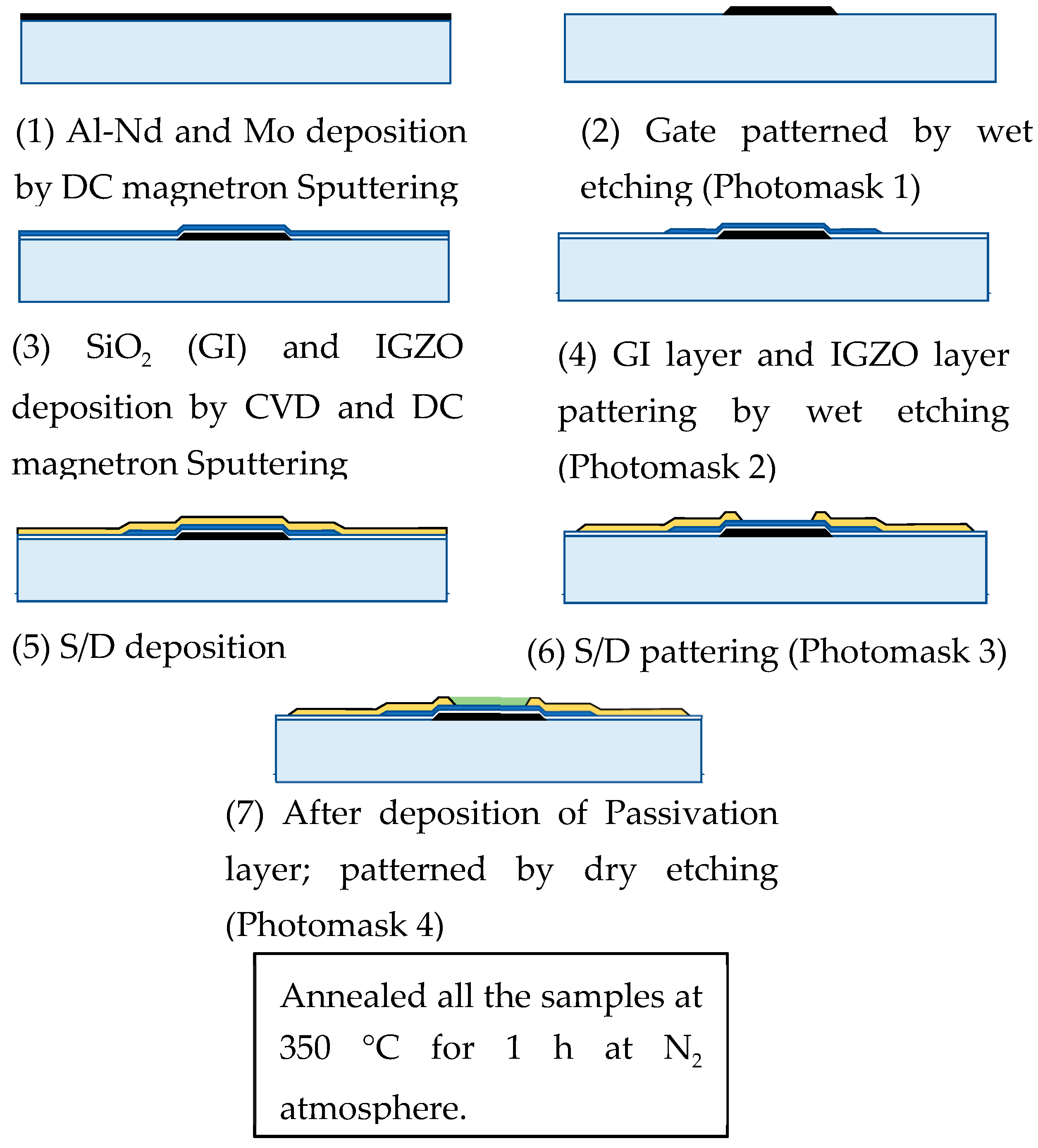
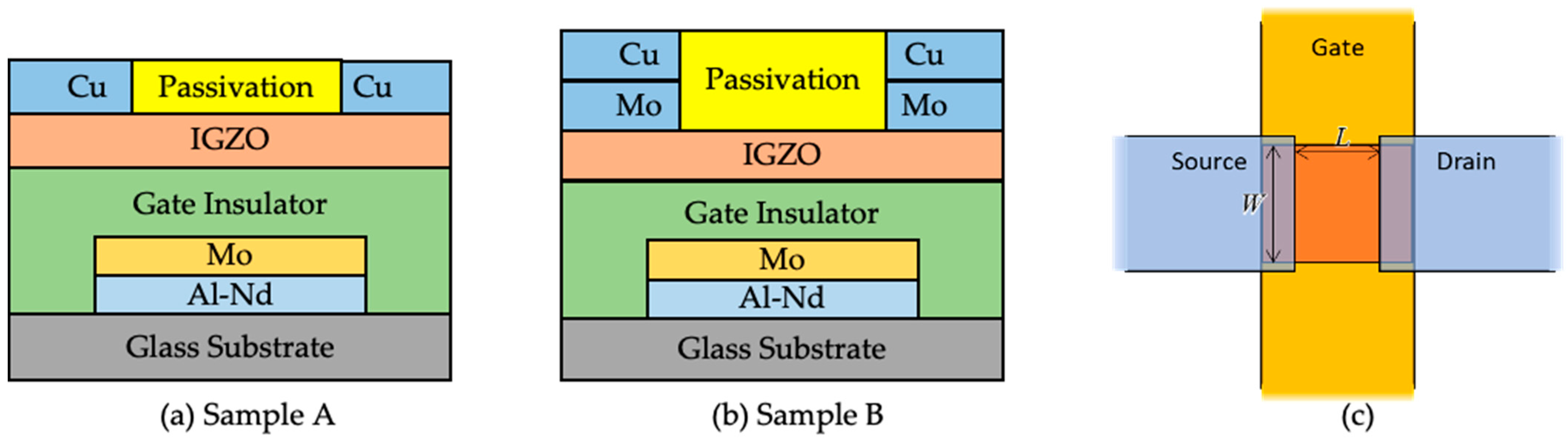
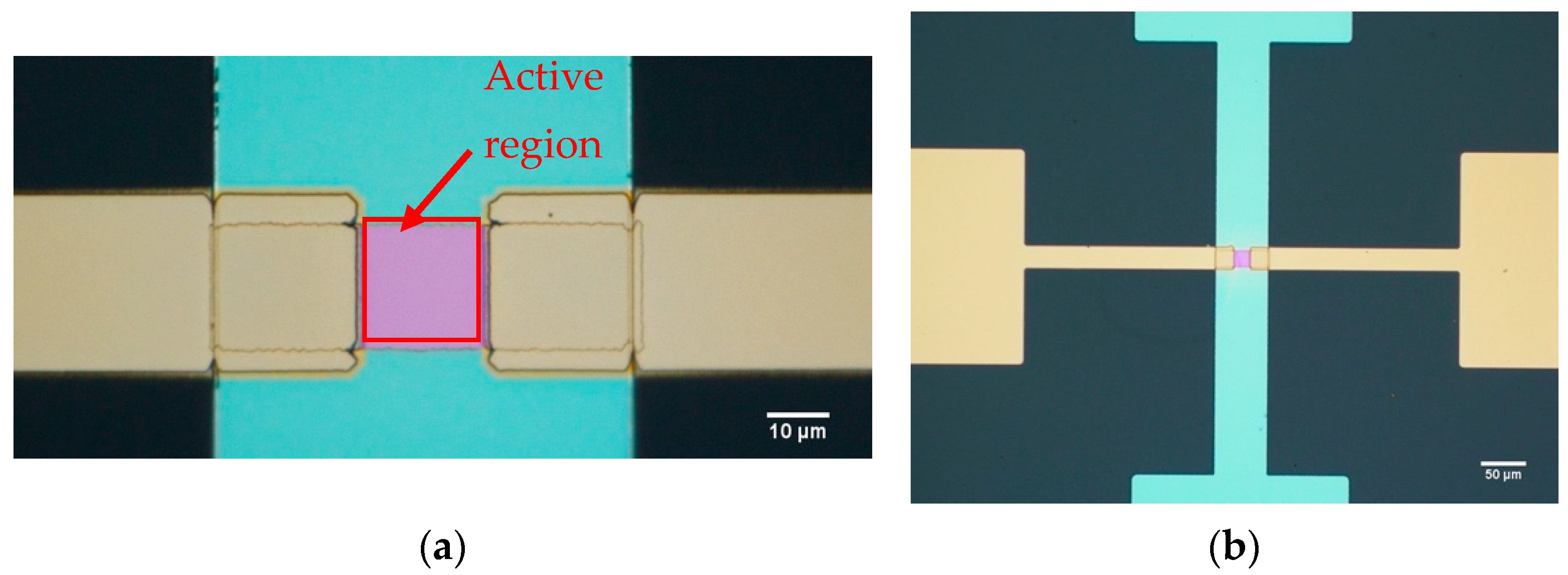
2. Experimental Details
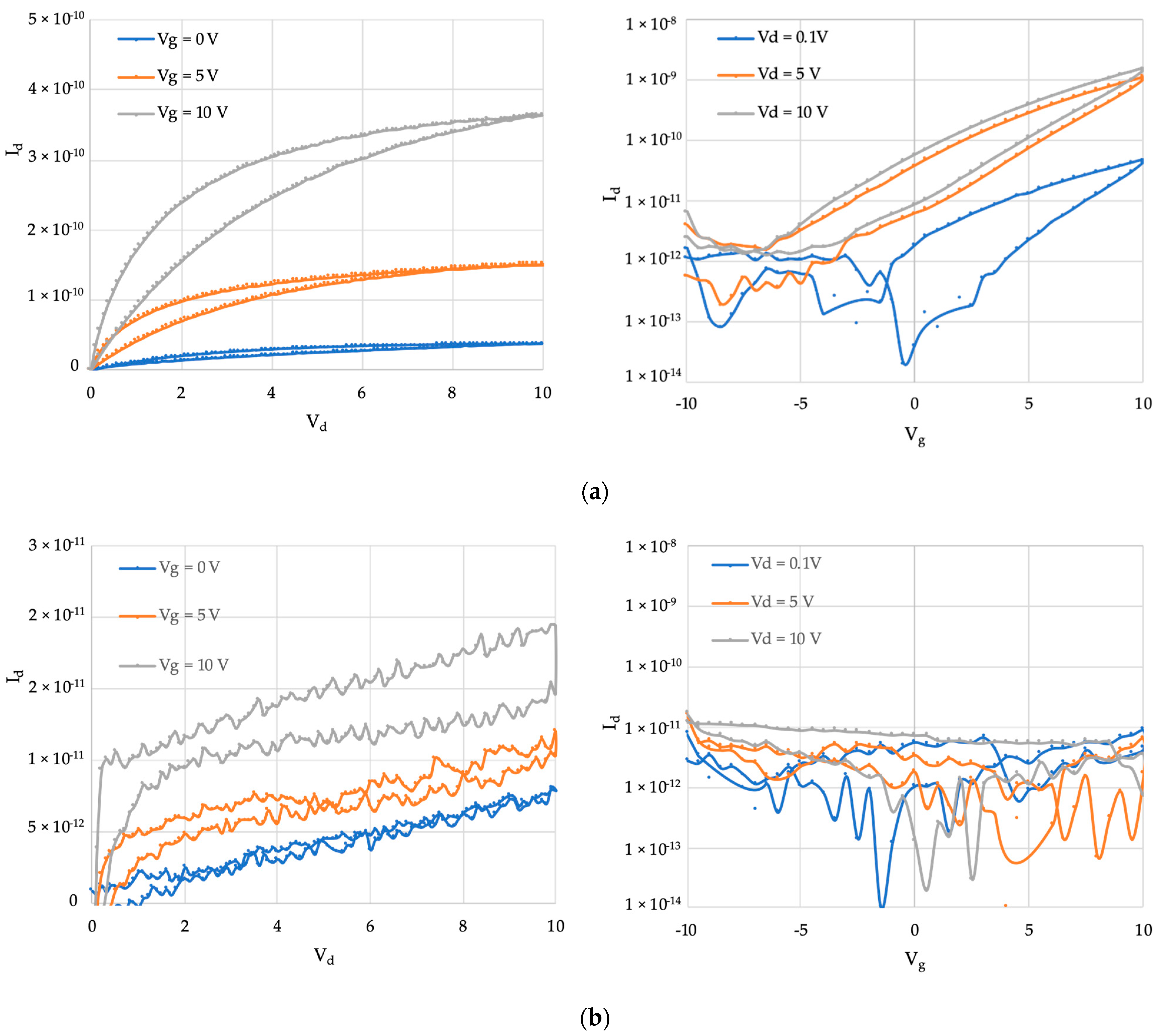
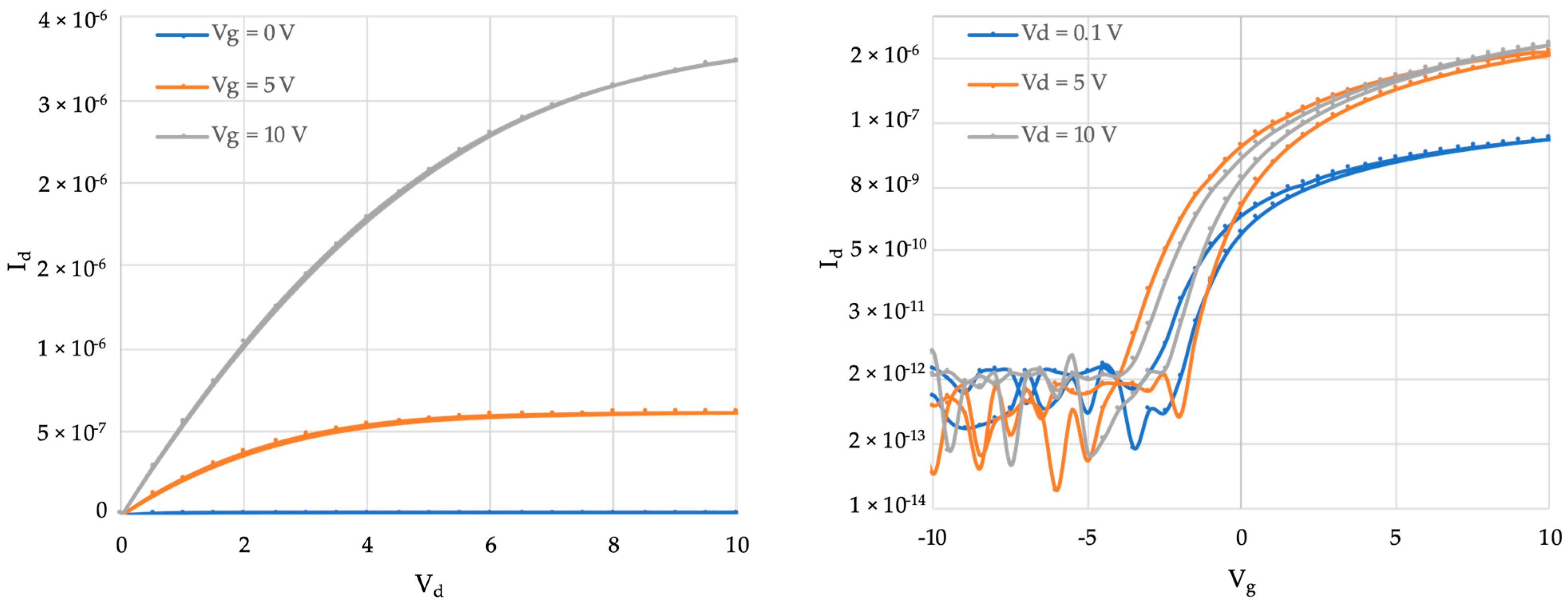
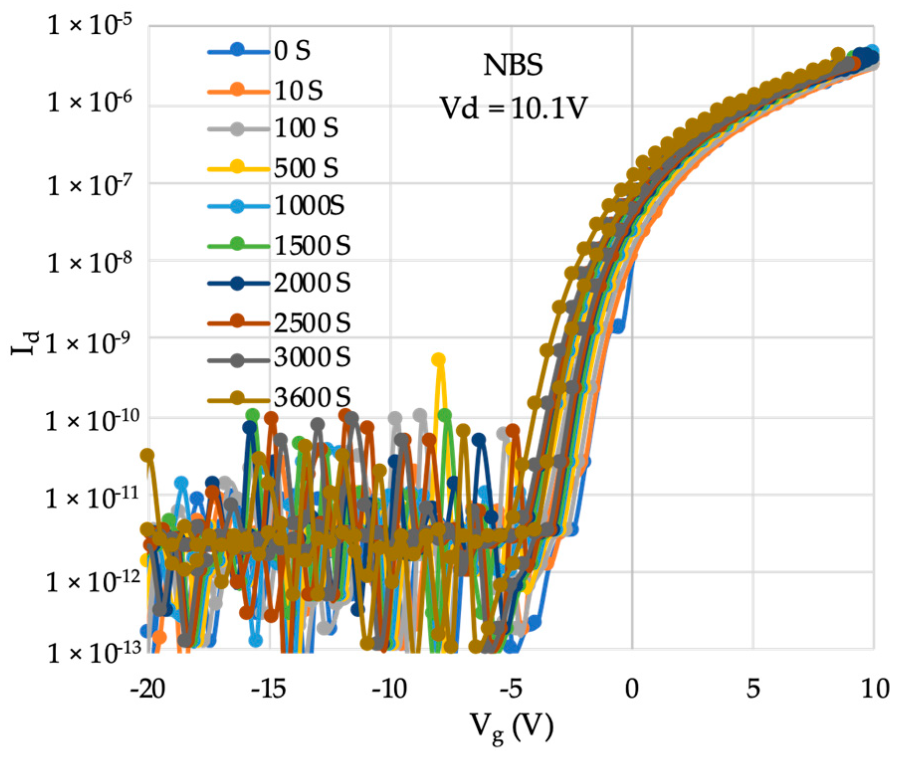
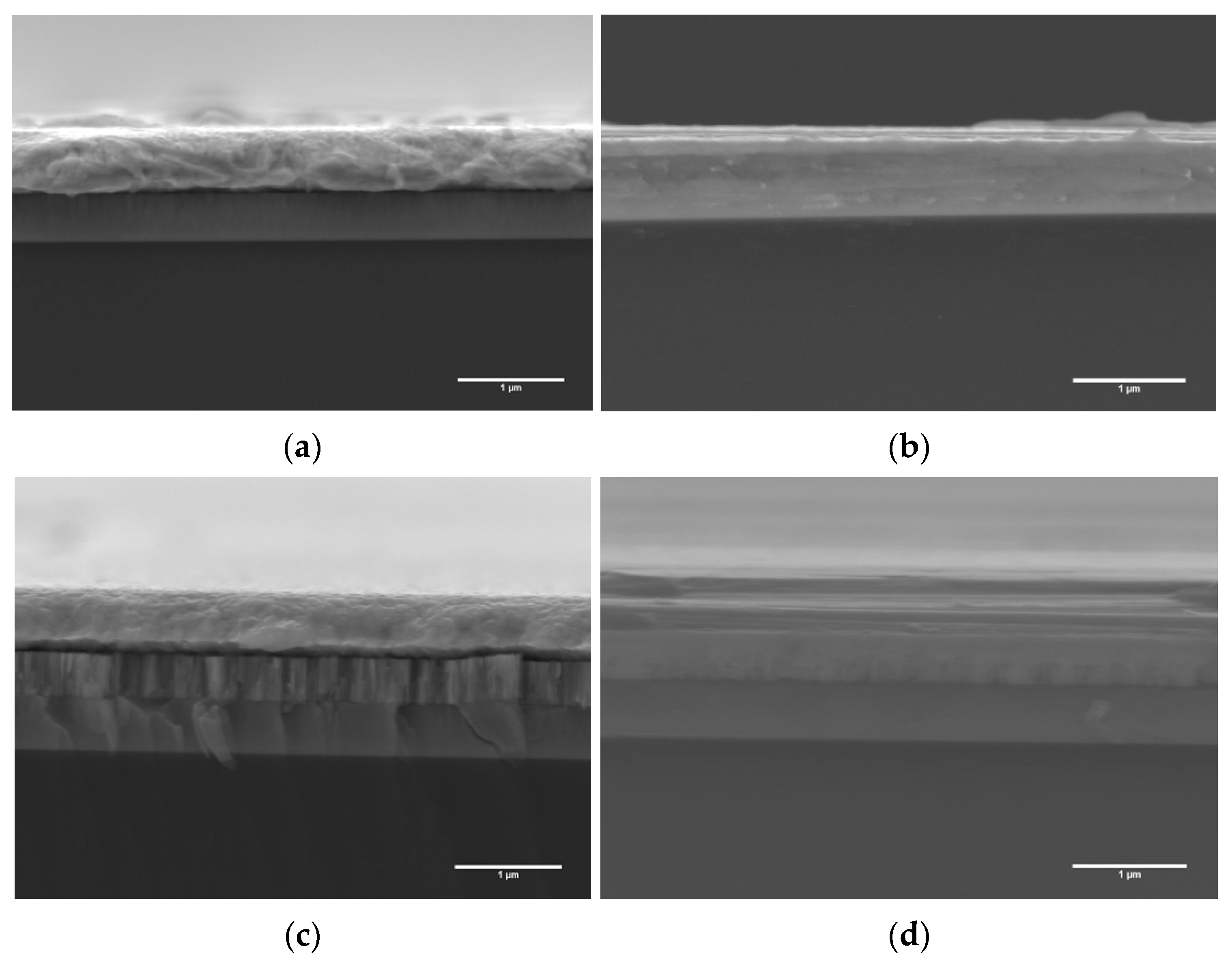
Figure 1 shows the process flow of the samples used in this report. An inverted staggered bottom-gate IGZO were prepared on a glass substrate. First, the gate electrode with Al-Nd (85 nm)/Mo (15 nm) was deposited on a glass substrate by DC magnetron sputtering. Al-Nd alloy was deposited to avoid the electro migration and Mo was used as a barrier layer. The gate electrode was patterned using the photolithography process and wet etching. Subsequently, a gate insulator (GI) of 150-nm thick SiO2 was formed using plasma-enhanced chemical vapor deposition (PECVD). Then, a 15-nm IGZO thin film as an active layer was deposited by DC magnetron sputtering in a gas mixture of Ar and Ar-O2 (90–10%) at 150 °C, from the ceramic target atomic ratio In:Ga:Zn = 1:1:1. The deposition chamber pressure was evacuated less than 1 × 10⁵ Pa and the working pressure was 1 Pa. Next, the active layer and GI layer was patterned. The oxygen partial pressure was calculated as [P (O2) = O2/(Ar + O2)] and fixed at 1%. A 40 nm of 99.999% pure Cu interlayer was deposited on patterned active layer for Sample A. Stacked films of 20 nm Mo and 40 nm Cu were deposited for sample B using thermal evaporation and patterned again the S/D contact for all samples. A thinner Cu layer was deposited to reduce contact resistance, but it is possible to deposit a thicker one. The special Cu etchant etched the Cu layer only, not the IGZO active layer. S/D were patterned by a photo mask and photolithography process. Active channel width and length were 10 µm and 20 µm, respectively. Finally, a 200 nm SiO2 passivation layer was deposited for both devices with a working pressure at 110 Pa at 200 °C by chemical vapor deposition (CVD) process. Furuta et al. reported that certain amounts of H2 may be diffused into the IGZO active layer from the passivation layer, which can act as a shallow donor in IGZO films [21]. This passivation layer also protects the device from external influence. The SiO2 passivation layer was deposited at the partial pressure of SiH4 of P[SiH4] = 1.36% using N2, SiH4 and N2O gases. This passivation layer was also patterned by a photolithography process to make the contact. Ultimately, all the devices were annealed at 350 °C at N2 environment for 1 h. The cross-sectional views of the TFT for Samples A and B are shown in Figure 2a,b, respectively, and the plane view is illustrated in Figure 2c. For the SEM and EDX analysis, 500 nm IGZO was deposited on the glass substrate. For the Cu diffusion analysis, 500 nm Cu was deposited on IGZO using a thermal evaporation process and evaluated before and after the annealing effect. To observe the effect of the barrier layer, 500 nm of Cu and Mo film was deposited on the IGZO thin film using thermal evaporation and DC sputtering process, and the before and after annealing effect was analyzed.

3. Results

The active layer defines the channel width, and the separation of S/D electrodes defines the channel length. In this design, we can define the channel width correctly by the active layer width, but the edge of the active layer has a chance to be damaged by the etching. As shown later, we have problems with SS value and leakage current even after improving the mobility value. Therefore, there is still plenty of room for improvement in the design of the TFT layout. Figure 3a,b shows the microscopic image of IGZO TFTs samples with no defects after using Cu etchant.
Ferric chloride (FeCl3), Cupric Chloride (CuCl2), Hydrogen peroxide—Sulphuric acid (H2O2-H2SO4), Chromic—Sulphuric acid (CrO3-H2SO4), ammonium persulphate (NH4)2SO4) and Citric acid are widely used as a Cu etchant; however, all of them contain strong acids, such as HCL and H2SO4 [22,23,24]. All the etchants have a high-etched rate, high-Cu dissolving capacity and are very acidic [25]. For this reason, those acidic Cu etchants can damage the IGZO layer and device structure easily and affect the device performance. As a result, most researchers use shadow mask to deposit S/D to avoid wet Cu etchant [20,26,27,28]. TFTs characteristics are usually presumed from the transfer characteristics, where the drain to source current (Id) is plotted against gate to source voltage (Vg) for various drain to source voltage (Vd) and from output characteristics, where Id is plotted against drain to source voltage (Vd) for various gate to source voltage (Vg), as shown in Figure 4. The parameters of the output characteristics and the transfer characteristics of sample A and B are as follows; the gate voltage (Vg) was 0 V, 5 V and 10 V and drain voltage was 0.1 V, 5 V and 10 V, respectively. At the value of drain voltage (Vd) at 1 V, the threshold voltage (Vth) represents the gate voltage (Vg) corresponding to the drain current (Id) of 1 × 10⁻⁹ A. The electrical characteristics of device performance are extracted by analyzing several parameters, such as saturation region mobility (μSAT), field-effect mobility (μFE), threshold voltage (Vth), On-Current (ION) and subthreshold swing (SS). The field-effect mobility is evaluated based on gradual channel approximation and the equation is as follows,
I d = W L   μ C i [   ( V g V t h ) V d V d 2 2 ]
Here, μ is the channel carrier mobility, W and L are channel width and length, and Ci is the gate capacitance per unit area of the insulator layer. Furthermore, the saturation region mobility was obtained from the curve of the square root of the drain current versus the Vg in saturation operation region:
I d = ( W C i μ S A T 2 L ) 1 / 2   ( V g V t h )
Another important parameter subthreshold swing (SS) reflects the change of Vg instead of increase Id; is determined by,
S S = d V g d l o g 10 ( I d )
Figure 4 represents the output and transfer characteristics of sample A. The electrical characteristics of Figure 4a are better compared to Figure 4b, though the mobility is tiny and threshold voltage is quite high. Figure 4a is the electrical properties of sample A, which are calculated before annealing the sample. Moreover, the electrical characteristics of sample A are becoming worst after post-annealing. The reason might be described by the diffusion of Cu into the IGZO layer for post annealing after the deposition of the Cu S/D contact or for depositing Cu onto the channel layer directly. Figure 4a has been extracted before annealing. Therefore, it has less chance of Cu diffusion into IGZO layer. Sample B has a 15-nm-thick Mo layer at the S/D contact, which makes ohmic contacts after annealing and prevents the diffusion of Cu into the IGZO layer. Figure 5 shows the output and transfer characteristics of sample B after post-annealing. The sample B for W/L of 10/20 (µm/µm) achieves improved performance as follows: Vth of 1.2 V, µSAT of 11 cm2/V-s, and ION of 3.16 × 10⁻⁶ A. This experimental data assured that the non-acidic selective Cu etchant has no effect on IGZO layer. The hysteresis has completely minimized from the output characteristics, but still there is hysteresis at the transfer characteristics. The SS value becomes high because the density of the acceptor-like trap states of IGZO is also increased. Hu et al. reported the field effect mobility around 11.5 cm2/V-s with ITO barrier layer [27]. On the other hand, Kim et al. also reported the field effect mobility around 12.8 cm2/V-s with Mo-Ti/Cu S/D [28]. These results are quite similar to our experimental results. Figure 6 shows the negative bias temperature stress at the drain voltage of 10.1 V. The transfer characteristics are shifted left from the threshold voltage of 1.2 V to 0.4 V, which improve the TFT characteristics. The H2 atom from the passivation layer may have been diffused into the IGZO layer due to of annealing, which can enhance the electrical properties. The IGZO TFT without a passivation layer does not exhibit remarkable electronic properties because it may be affected by external influence (see the Supplementary File, Figure S1). Table 1 exhibits the details analysis between sample A and B after post-annealing. The electrical performance of the TFTs is summarized in Table 1.
Figure 7 shows the SEM image of the sample A and B. In Figure 7a, the Cu layer and the IGZO thin film is completely separated from each other. From the mapping analysis and EDX layered analysis, the image also shows the clear demonstration of each layer (see the Supplementary File, Figure S2). The spectrum analysis of sample A before post annealing shows the individual peak intensity of Cu, In, Ga and Zn (See the Supplementary File, Figure S3). However, after post annealing the Cu was diffused into the IGZO layer. For this reason, the thickness of Cu layer was decreased. The mapping analysis of EDX layered analysis also reveals the clear demonstration of Cu diffusion (red dots) (See the Supplementary File, Figure S4). The spectrum analysis of sample A after post annealing also shows the Cu peaks into the IGZO active layer. It clearly shows that Cu is diffusing into the IGZO layer after post annealing, which deteriorated the electrical properties of IGZO TFTs. It also shows the peak intensity of Cu, In, Ga and Zn (See the Supplementary File, Figure S5) into the IGZO layer. The IGZO region near the IGZO-CU interfacial layer contains a large amount of Cu, but this decreased at the deeper region of IGZO. Before post annealing of sample B (Figure 7c), the stacked layer of Mo/Cu and the IGZO layer has been seen clearly. After post annealing (Figure 7d), the Mo layer is clearly seen in between Cu and IGZO layer. Here the Mo layer is acting as a barrier layer to prevent the Cu diffusion. The EDX-layered analysis of sample B before annealing shows the separate color dot of each material that confirms that there is no Cu diffusion of Cu into IGZO layer before post annealing (See the Supplementary File, Figure S6). On the other hand, Figure 7c clearly shows that the Cu cannot diffused into IGZO after post annealing. The stack layer of Mo can prevent the Cu diffusion. The EDX layered analysis and spectrum analysis of Sample B after post annealing also shows the clear representation of each layer. There are no peaks of Cu into the IGZO layer in the spectrum analysis, which clearly determines that in the Mo/Cu S/D IGZO TFTs, the Cu cannot diffuse into IGZO due to the Mo barrier layer (See the Supplementary File, Figure S7). This phenomenon also supports the enhancement the electrical characteristics.

4. Conclusions

In summary, we have successfully fabricated a high mobility IGZO TFT with Mo-Cu S/D contact using a special non-acidic Cu etchant, which can etch Cu properly and avoid the damage to IGZO layer. The electrical properties of IGZO TFTs with Mo/Cu S/D ensure the selectivity of Cu etchant. Post-annealing treatment formed and improved the TFT characteristics, and the Mo interlayer prevented the Cu diffusion into active layer. The SEM image analysis clearly shows evidence of the prevention of Cu diffusion with the Mo layer. The mapping and spectrum analysis also clarify the diffusion mechanism. Thus, the TFT with Mo-Cu S/D exhibited proper switching characteristics with saturation mobility at 11 cm2/V-s. The results suggested an effective fabrication method for fabricating high-mobility metal oxide TFT based on Cu S/D.

Supplementary Materials

The following are available online at https://0-www-mdpi-com.brum.beds.ac.uk/article/10.3390/pr9122193/s1, Figure S1: Output and transfer characteristics of IGZO TFT without passivation layer after annealing in N2 atmosphere for 1 hour. Figure S2: Mapping analysis of sample A before post annealing. Figure S3: Spectrum analysis of sample A before post annealing. Figure S4: Mapping analysis of sample A after post annealing. Figure S5: Spectrum analysis of sample A after post annealing. Figure S6: The EDX layered analysis of Sample B before post annealing. Figure S7: The EDX layered analysis and spectrum analysis of Sample B after post annealing.

Author Contributions

Conceptualization, R.K. and R.H.; methodology, R.K. and R.H.; software, R.K.; validation, formal analysis, R.K., M.A.B.M., M.O., J.T.S., T.I. and R.H.; investigation, R.K., M.A.B.M. and J.T.S.; resources, R.K. and R.H.; data curation, R.K. and M.A.B.M.; writing—original draft preparation, R.K.; writing—review and editing, R.H.; supervision, R.H. All authors have read and agreed to the published version of the manuscript.

Funding

This research received no external funding.

Institutional Review Board Statement

Not applicable.

Informed Consent Statement

Not applicable.

Data Availability Statement

The data that support the findings of this study are available from the corresponding author upon reasonable request.

Acknowledgments

The support from Kyushu University and the Ministry of Education, Culture, Sports, Science, and Technology (MEXT), Japan, is highly appreciated.

Conflicts of Interest

The authors declare no conflict of interest.

References

  1. Nomura, K.; Takagi, A.; Kamiya, T.; Ohta, H.; Hirano, M.; Hosono, H. Amorphous oxide semiconductors for high-performance flexible thin-film transistors. Jpn. J. Appl. Phys. 2006, 45, 4303. [Google Scholar] [CrossRef]
  2. Nomura, K.; Ohta, H.; Takagi, A.; Kamiya, T.; Hirano, M.; Hosono, H. Room-temperature fabrication of transparent flexible thin-film transistors using amorphous oxide semiconductors. Nature 2004, 432, 488–492. [Google Scholar] [CrossRef]
  3. Nomura, K.; Ohta, H.; Ueda, K.; Kamiya, T.; Hirano, M.; Hosono, H. Thin-film transistor fabricated in single-crystalline transparent oxide semiconductor. Science 2003, 300, 1269–1272. [Google Scholar] [CrossRef]
  4. Park, J.S.; Maeng, W.J.; Kim, H.S.; Park, J.S. Review of recent developments in amorphous oxide semiconductor thin-film transistor devices. Thin Solid Film. 2012, 520, 1679–1693. [Google Scholar] [CrossRef]
  5. Martins, J.; Bahubalindruni, P.; Rovisco, A.; Kiazadeh, A.; Martins, R.; Fortunato, E.; Barquinha, P. Bias stress and temperature impact on InGaZnO TFTs and circuits. Materials 2017, 10, 680. [Google Scholar] [CrossRef] [Green Version]
  6. Fujimoto, Y.; Uenuma, M.; Ishikawa, Y.; Uraoka, Y. Analysis of thermoelectric properties of amorphous InGaZnO thin film by controlling carrier concentration. AIP Adv. 2015, 5, 097209. [Google Scholar] [CrossRef]
  7. Khan, R.; Ohtaki, M.; Hata, S.; Miyazaki, K.; Hattori, R. Thermal conductivity of nano-crystallized indium-gallium-zinc oxide thin films determined by differential three-omega method. Nanomaterials 2021, 11, 1547. [Google Scholar] [CrossRef] [PubMed]
  8. Sarswat, P.K.; Sarkar, S.; Yi, G.; Free, M.L. Phosphorus-doped SnTe-type needle-like crystals: Band structure modifications and electronic properties. J. Phys. Chem. C 2017, 121, 18263–18273. [Google Scholar] [CrossRef]
  9. Oh, T. Analysis of surface current by quantum tunneling effect of thin film transistors with topological insulators. Sci. Rep. 2020, 10, 9509. [Google Scholar] [CrossRef]
  10. Lee, S.H.; Oh, D.J.; Hwang, A.Y.; Han, D.S.; Kim, S.; Jeong, J.K.; Park, J.W. Improvement in device performance of a-InGaZnO transistors by introduction of Ca-doped Cu source/drain electrode. IEEE Electron Device Lett. 2015, 36, 802–804. [Google Scholar] [CrossRef]
  11. Zhao, M.; Xu, M.; Ning, H.; Xu, R.; Zou, J.; Tao, H.; Wang, L.; Peng, J. Method for fabricating amorphous indium-zinc-oxide thin-film transistors with copper source and drain electrodes. IEEE Electron Device Lett. 2015, 36, 342–344. [Google Scholar] [CrossRef]
  12. Arai, T. Oxide-TFT technologies for next-generation AMOLED displays. J. Soc. Inf. Disp. 2012, 20, 156–161. [Google Scholar] [CrossRef]
  13. Kim, W.-S.; Moon, Y.-K.; Kim, K.-T.; Lee, J.-H.; Ahn, B.-D.; Park, J.-W. An investigation of contact resistance between metal electrodes and amorphous gallium-indium-zinc oxide (a-GIZO) thin-film transistors. Thin Solid Film. 2010, 518, 6357–6360. [Google Scholar] [CrossRef]
  14. Yim, J.R.; Jung, S.Y.; Yeon, H.W.; Kwon, J.Y.; Lee, Y.J.; Lee, J.H.; Joo, Y.C. Effects of metal electrode on the electrical performance of amorphous In-Ga-Zn-O thin film transistor. Jpn. J. Appl. Phys. 2012, 51, 011401. [Google Scholar] [CrossRef] [Green Version]
  15. Hu, S.; Fang, Z.; Ning, H.; Tao, R.; Liu, X.; Zeng, Y.; Yao, R.; Huang, F.; Li, Z.; Xu, M.; et al. Effect of post treatment for cu-cr source/drain electrodes on a-igzo tfts. Materials 2016, 9, 623. [Google Scholar] [CrossRef] [Green Version]
  16. Youn, C.S.; Lee, D.G. Effects of post heat treatment on the mechanical properties of cold-rolled Ti/Cu clad sheet. Metals 2020, 10, 1672. [Google Scholar] [CrossRef]
  17. Fisher, I.; Eizenberg, M. Copper ion diffusion in porous and nonporous SiO2-based dielectrics using bias thermal stress and thermal stress tests. Thin Solid Film. 2008, 516, 4111–4121. [Google Scholar] [CrossRef]
  18. Choi, K.-H.; Kim, H.-K. Correlation between Ti source/drain contact and performance of InGaZnO-based thin film transistors. Appl. Phys. Lett. 2013, 102, 052103. [Google Scholar] [CrossRef] [Green Version]
  19. Lan, L.; Xu, M.; Peng, J.; Xu, H.; Li, M.; Luo, D.; Zou, J.; Tao, H.; Wang, L.; Yao, R. Influence of source and drain contacts on the properties of the indium-zinc oxide thin-film transistors based on anodic aluminum oxide gate dielectrics. J. Appl. Phys. 2011, 110, 103703. [Google Scholar] [CrossRef]
  20. Hu, S.; Ning, H.; Lu, K.; Fang, Z.; Li, Y.; Yao, R.; Xu, M.; Wang, L.; Peng, J.; Lu, X. Mobility enhancement in amorphous in-Ga-Zn-O thin-film transistor by induced metallic in nanoparticles and Cu electrodes. Nanomaterials 2018, 8, 197. [Google Scholar] [CrossRef] [Green Version]
  21. Toda, T.; Wang, D.; Jiang, J.; Hung, M.P.; Furuta, M. Quantitative analysis of the effect of hydrogen diffusion from silicon oxide etch-stopper layer into amorphous In-Ga-Zn-O on thin-film transistor. IEEE Trans. Electron Devices 2014, 61, 3762–3767. [Google Scholar] [CrossRef]
  22. Çakır, O. Review of etchants for copper and its alloys in wet etching processes. Key Eng. Mater. 2007, 364, 460–465. [Google Scholar] [CrossRef]
  23. Williams, K.R.; Gupta, K.; Wasilik, M. Etch rates for micromachining processing—Part II. J. Microelectromech. Syst. 2003, 12, 761–778. [Google Scholar] [CrossRef] [Green Version]
  24. Georgiadou, M.; Alkire, R. Anisotropic chemical etching of copper foil: II. experimental studies on shape evolution. J. Electrochem. Soc. 1993, 140, 1348–1355. [Google Scholar] [CrossRef]
  25. Noma, H.; Nakanishi, T. Etching process analysis based on etchant flow for high-density build-up substrate. In Proceedings of the 6th Electronics Packaging Technology Conference, EPTC 2004, Singapore, 8–10 December 2004. [Google Scholar] [CrossRef]
  26. Hu, S.; Ning, H.; Lu, K.; Fang, Z.; Tao, R.; Yao, R.; Zou, J.; Xu, M.; Wang, L.; Peng, J. Effect of Al2O3 passivation layer and Cu electrodes on high mobility of amorphous IZO TFT. IEEE J. Electron Devices Soc. 2018, 6, 733–737. [Google Scholar] [CrossRef]
  27. Hu, S.; Lu, K.; Ning, H.; Fang, Z.; Liu, X.; Xie, W.; Yao, R.; Zou, J.; Xu, M.; Peng, J. Effect of ITO serving as a barrier layer for Cu electrodes on performance of a-IGZO TFT. IEEE Electron Device Lett. 2018, 39, 504–507. [Google Scholar] [CrossRef]
  28. Kim, L.Y.; Kwon, O.K. Effects of stacked Mo-Ti/Cu source and drain electrodes on the performance of amorphous In-Ga-Zn-O thin-film transistors. IEEE Electron Device Lett. 2018, 39, 43–46. [Google Scholar] [CrossRef]
Figure 1. Process flow of bottom gate top contact IGZO TFTs.
Processes 09 02193 g001
Figure 2. Schematic cross-section of the IGZO TFT on a glass substrate with a bottom-gate top-contact structure. (a) Sample A, (b) Sample B, and (c) top view of the IGZO TFTs.
Processes 09 02193 g002
Figure 3. (a,b) Microscopic image of bottom gate top contact IGZO TFTs after using the special Cu etchant at different magnification.
Processes 09 02193 g003
Figure 4. Output (left side) and transfer characteristics (right side) of sample A (a) Pre-annealing and (b) post-annealing.
Processes 09 02193 g004
Figure 5. Output (left side) and transfer characteristics (right side) of sample B after annealing.
Processes 09 02193 g005
Figure 6. Changes in transfer characteristics under negative-bias temperature stress at the range of gate voltage from −20 V to 10 V.
Processes 09 02193 g006
Figure 7. Scanning electron microscopy image of sample A (a) before post-annealing, (b) after post annealing, and sample B (c) before post-annealing, (d) after post annealing.
Processes 09 02193 g007
Table 1. The electrical properties of IGZO TFTs.
S/DμFE (cm2/V-s)μSAT (cm2/V-s)Vth (V)ION (A)SS (V/Decade)Annealing Condition
Cu9.2 × 10−51.8 × 10−551.6 × 10⁻⁹-Before Post-annealing
Mo/Cu12.3111.23.2 × 10−60.58After Post-annealing
Publisher’s Note: MDPI stays neutral with regard to jurisdictional claims in published maps and institutional affiliations.

