Diffraction Efficiency Characteristics for MEMS-Based Phase-Only Spatial Light Modulator with Nonlinear Phase Distribution


James C. Wyant College of Optical Sciences, University of Arizona, Tucson, AZ 85721, USA
*
Author to whom correspondence should be addressed.
Photonics 2021, 8(3), 62; https://0-doi-org.brum.beds.ac.uk/10.3390/photonics8030062
Submission received: 28 January 2021
/
Revised: 16 February 2021
/
Accepted: 19 February 2021
/
Published: 24 February 2021
(This article belongs to the Special Issue Holography)
Abstract
:Micro-electro mechanical systems (MEMS)-based phase-only spatial light modulators (PLMs) have the potential to overcome the limited speed of liquid crystal on silicon (LCoS) spatial light modulators (SLMs) and operate at speeds faster than 10 kHz. This expands the practicality of PLMs to several applications, including communications, sensing, and high-speed displays. The complex structure and fabrication requirements for large, 2D MEMS arrays with vertical actuation have kept MEMS-based PLMs out of the market in favor of LCoS SLMs. Recently, Texas Instruments has adapted its existing DMD technology for fabricating MEMS-based PLMs. Here, we characterize the diffraction efficiency for one of these PLMs and examine the effect of a nonlinear distribution of addressable phase states across a range of wavelengths and illumination angles.
1. Introduction
Most 2D arrayed spatial light modulators (SLMs) currently available commercially are based on either liquid crystals on silicon (LCoS) or micromirror arrays. Liquid crystal SLMs work on the principle of birefringence in electro-optical liquid crystals. A bias placed across a liquid crystal cell results in rotation of the liquid crystal molecules, and the phase retardation of light through the crystal can be modified. Unfortunately, even after years of research, commercial LCoS SLMs are still limited in their refresh speed to sub kHz due to the viscoelasticity of the liquid crystal material [1].
Micromirror devices are micro-electro mechanical systems (MEMS) that comprise of arrays of moveable mirrors, on the scale of microns, to modulate light. Because their speed is only limited by the resonance frequency of the micro-mirror, these MEMS are capable of refresh rates that are tens of kHz [2]. The most commonly available micromirror SLMs are the Texas Instruments’ Digital Light Processing (DLP) line of Digital Micromirror Devices (DMDs) [3]. Historically, DMDs were amplitude-only modulators, meaning that the intensity of the light is modulated, and the phase is not. DMD works by tilting the micromirrors between two states, sending the light in two directions. When the mirrors are in one state, the light is directed toward the open aperture of the system, while when in the other state, the light is typically discarded. This results in low optical efficiency. A DMD can also be used as a diffractive element when displaying not an image, but a hologram. Because the DMD can only display binary amplitude holograms, its diffraction efficiency is limited to 10% [4].
A phase-only, MEMS-based SLM would be much more efficient in projecting holograms, starting at 40.5% for binary levels with phase modulation, and increasing from there when additional phase levels are accessible. A phase-only MEMS can be made by actuating the micromirrors vertically in piston motion.
Due to the complexity of the fabrication for micromirror devices with large numbers of pixels, MEMS-based phase-only spatial light modulator (PLM) devices have had limited practical use [5]. In recent years, Texas Instruments has begun to adapt existing technology from its DMD line to develop a micromirror PLM with piston mode actuation [6]. The current version of this device consists of a 960 × 540 array of 10.5 m square mirrors.
While LCoS SLMs are the incumbent technology for phase light modulation, the MEMS-based alternative has several advantages. As we already introduced, the biggest advantage of the MEMS PLM is the switching speed. Due to the slow free-energy relaxation of liquid crystals, LCoS devices can only operate at sub kHz speeds [1]. MEMS, on the other hand, can switch at speeds on the order of tens of kHz. While LCoS speeds may allow for standard video projection at 180 Hz, it is not suitable for techniques that involve temporally multiplexing images for increased resolution and image quality, or applications that require fast refresh rates, such as LiDAR beam scanning [7,8] or photonic optical switch [5]. MEMS-based devices also will not suffer from the same fringing field crosstalk between adjacent pixels as seen in LCoS, and are polarization-independent; thus, they do not require the polarization of the illuminating field to be specifically aligned, as is required by liquid crystals [9]. Potentially, MEMS might also be less affected by scattering and might sustain higher illumination power since the light does not have to be transmitted through a medium, but is directly reflected by the micro-mirror’s surface.
Phase light modulation has applications across the spectrum from lithography [10,11] in the UV, to displays including augmented and virtual reality, as well as holographic 3D display [8,12], to communications and LiDAR in the near-infrared [5,7]. All of these applications take advantage of the PLM’s ability to engineer the wavefront to redirect light more efficiently than amplitude modulation.
Here we present a model for the diffraction efficiencies of a PLM across the visible spectrum and examine the effect of illumination at oblique angles of incidence. We compare this model with measurement taken with the new PLM from Texas Instruments, and we look at the linearization of the phase levels for beam steering using a blazed diffraction grating implemented on the PLM device.
2. Theory
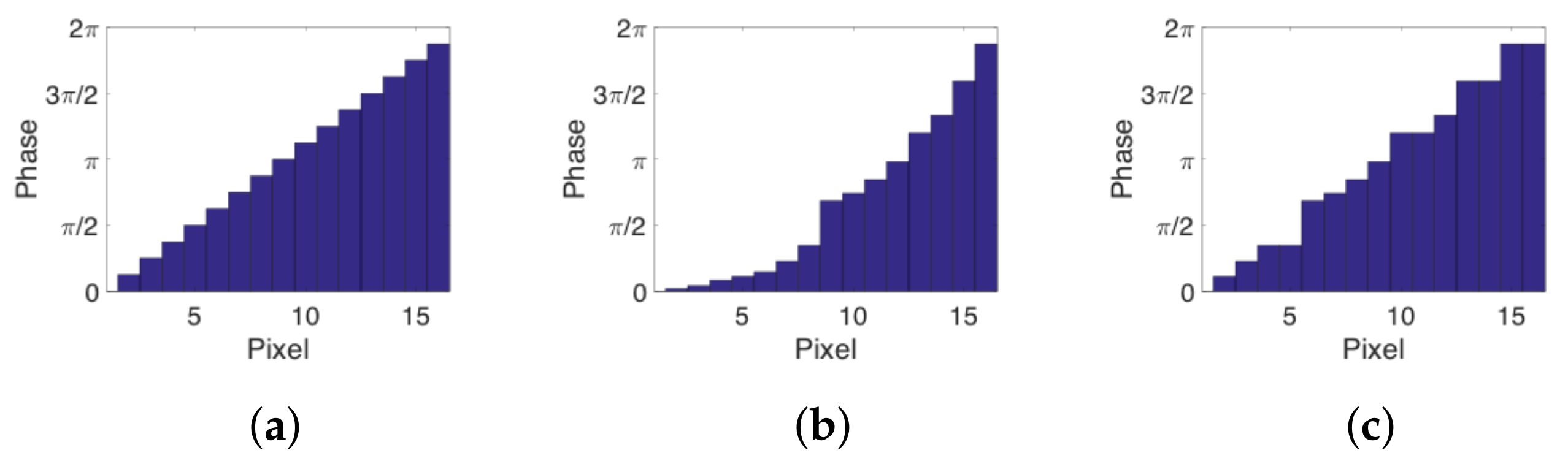
Blazed gratings are one-dimensional diffractive optical elements consisting of a periodic sawtooth phase profile. In the case of pixelated SLM or PLM, the profile is discretized to the available phase levels of the device, as shown in Figure 1.
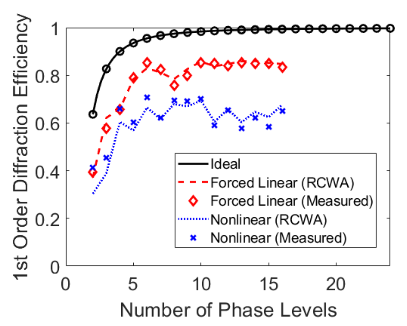
For the ideal case of a linear ramp of N steps, the first-order diffraction efficiency at normal incidence, shown in Figure 2, can be determined analytically as:
For a 16-level system (Figure 1a), this predicts a first-order efficiency of 98.7%. However, the actual distribution of the available phase levels on a particular device is not linear but follows a specific pattern, such as that presented in Figure 1b. This distribution has an linearity of 0.93 which reduces the efficiency to 72.5% at normal incidence for 532 nm illumination. Figure 1c is a forced linear mapping using the available phase levels (Figure 1b), which will be discussed later.
Diffraction efficiencies for the nonlinear phase distributions presented in Figure 1 were numerically simulated using Rigorous Coupled Wave Analysis (RCWA) using the DiffractMOD package in Rsoft by Synopsys [13]. The structure was modeled as a 2D reflective (aluminum) structure with a mirror pitch of 10.5 μm and mirror heights assigned to create the phase distributions seen in Figure 1 upon reflection at 532 nm at normal incidence. Then, the first-order diffraction efficiency was computed for each operating wavelength between [450 nm, 850 nm], and angle of incidences between [−85°, 85°].
3. Methods
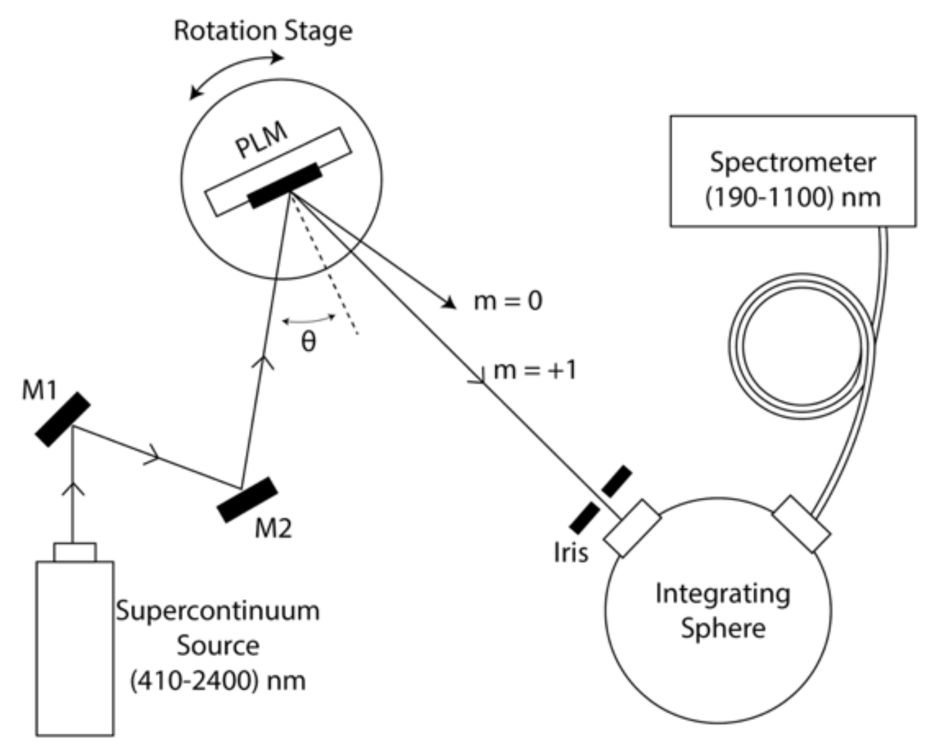
The diffraction efficiencies were measured using the configuration shown in Figure 3.
A supercontinuum laser source (SuperK Extreme from NKT Photonics) was used for simultaneous characterization of diffraction efficiency across a broad range of wavelengths. Diffraction orders were picked out using a rectangular aperture and measured using an integrating sphere connected to a spectrometer with a fiber optic cable. The device was mounted on a rotation stage and aligned such that the axis of rotation was at the surface of the PLM. Different angles of incidence were set by manually rotating the rotation stage and aligning the integrating sphere to the desired diffractive order.
The available phase levels shown in Figure 1b were measured using a Michelson interferometer with a 532 nm CW laser. For each of the phase levels, all mirrors in the device were set to the same height and the resulting fringe pattern was recorded. Relative phase differences between each of the levels was determined based on the shift of the fringes from one state to another. We observed that on our particular device, lower phase states are sampled much better than the higher phase states.
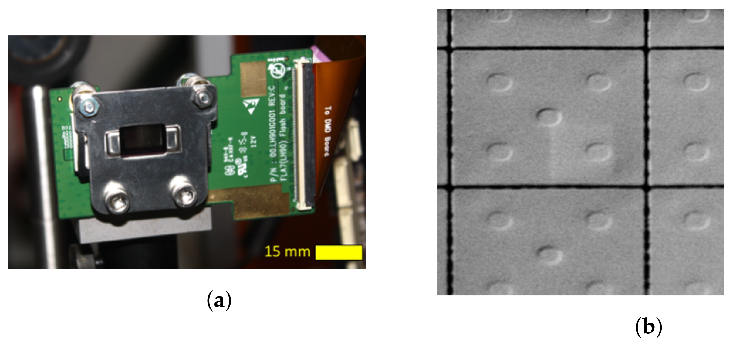
The PLM under test, presented in Figure 4, had a reflection efficiency of 63% at 532 nm when the device was set to a completely flat state. This is due to a combination of the mirror reflectivity (92% at 532 nm), the fill factor (94.5%), the cover glass reflections, and the overall mirror morphology, which is not perfectly flat (see Figure 4b). The individual mirrors are square with a side length of 10.5 um and a 0.3 um gap between each mirror. The average peak-to-valley height deviation of the surface of each mirror is 30 nm. The PLM housing also consists of protective cover glass with a broadband (400–700 nm) antireflective coating. To remove the device-specific characteristics, the diffraction efficiencies presented here are relative to the reflection efficiency of the PLM.
The phase levels of the PLM are modulated by encoding phase values to a 2 × 2 CMOS array under each mirror. The CMOS cells provide a 0 V or 10 V bias to individual electrodes beneath each mirror. By modulating which electrodes are biased, the effective area of the bias is changed, altering the electrostatic force on the mirror, allowing for 16 unique phase levels [6]. Two-dimensional phase patterns were generated on a computer and encoded for the CMOS scheme, then streamed to the device via HDMI (at 60 Hz) connected to a LightCrafter 4710 EVM board manufactured by Texas Instruments. The device is designed such that phase shift tuning to accommodate different wavelengths can be done by adjusting a separate mirror bias. At the tuned wavelength, the PLM mirrors can be actuated to provide a maximum deflection of half a wave, resulting in up to a full wave modulation after reflection. Actuation to the maximum deflection can be done in less than 20 μs and return in less than 10 μs [6]. For the purposes of this study, this bias was tuned to be optimal for 532 nm illumination for all measurements. Similar trends are observed for any tuned wavelength when illuminated with shorter or longer wavelength light.
4. Results and Discussion
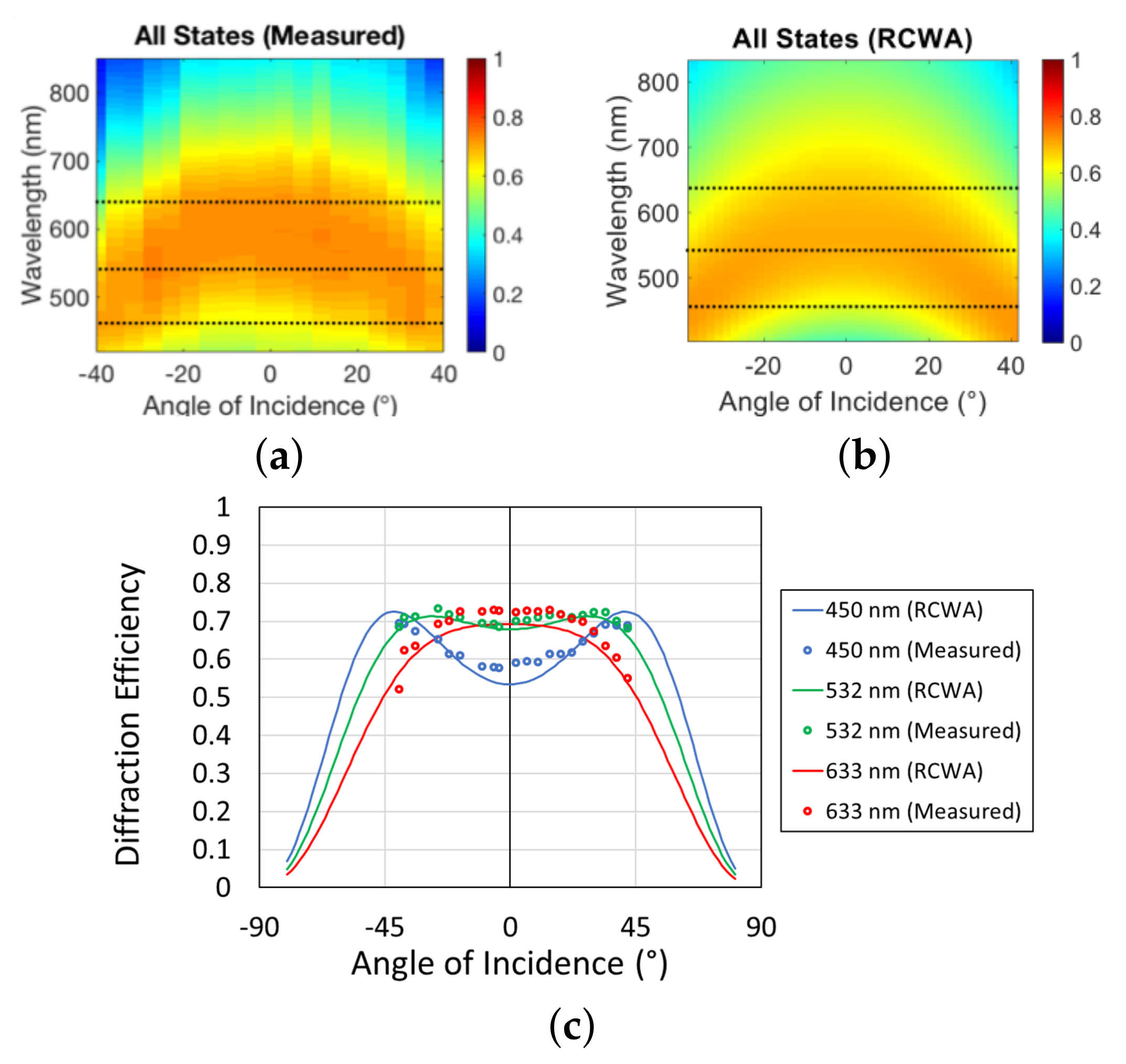
To measure the diffraction efficiency according to the wavelength and angle, the PLM was given a periodic blazed grating pattern consisting of a ramp of all 16 available phase levels (Figure 1b). Due to the limited fill factor of the PLM (10.5 μm pixels with a 0.3 μm gap), the device was still diffracting some amount of light when all mirrors were set to the same height. Therefore, the maximum first-order diffraction efficiency in Equation 1 is relative to the 0th-order efficiency of the flat-state device. This relative diffraction efficiency across the visible spectrum for the phase grating using all available PLM phase states is presented in Figure 5.
Around the wavelength at which the device is tuned to (532 nm), the diffraction efficiency is maximum over a broad range of incidence angles. In this region, there are subtle side lobes to the diffraction efficiency that approach 0° as the wavelength increases and spread away from 0° as wavelengths decrease. At a certain point, these side lobes merge and the diffraction efficiency became a single central peak at normal incidence. Beyond this point, the peak diffraction efficiency remains at normal angle of incidence, but the magnitude decreases as the overall phase modulation grows smaller compared to the incident wavelength.
As the wavelength decreases, the phase modulation range becomes larger than the incident wavelength. At normal incidence, the effective optical path difference is no longer optimal, and thus the peak diffraction efficiency occurs at non-normal angles of incidence. As the wavelength gets smaller, the spread of the side lobes increases, and the peak-to-valley diffraction efficiency also increases. For 450 nm incident light, the peak-to-valley efficiency difference is 10%. This could be significant for applications like lithography that require speed and high efficiency.
To optimize the efficiency at higher wavelength (>750 nm), the travel range of the micromirror needs to be increased. This will allow the PLM to operate in the IR region, especially at 1550 nm wavelength that is especially useful for telecommunication.
4.1. Impact of Linearity on Diffraction Efficiency
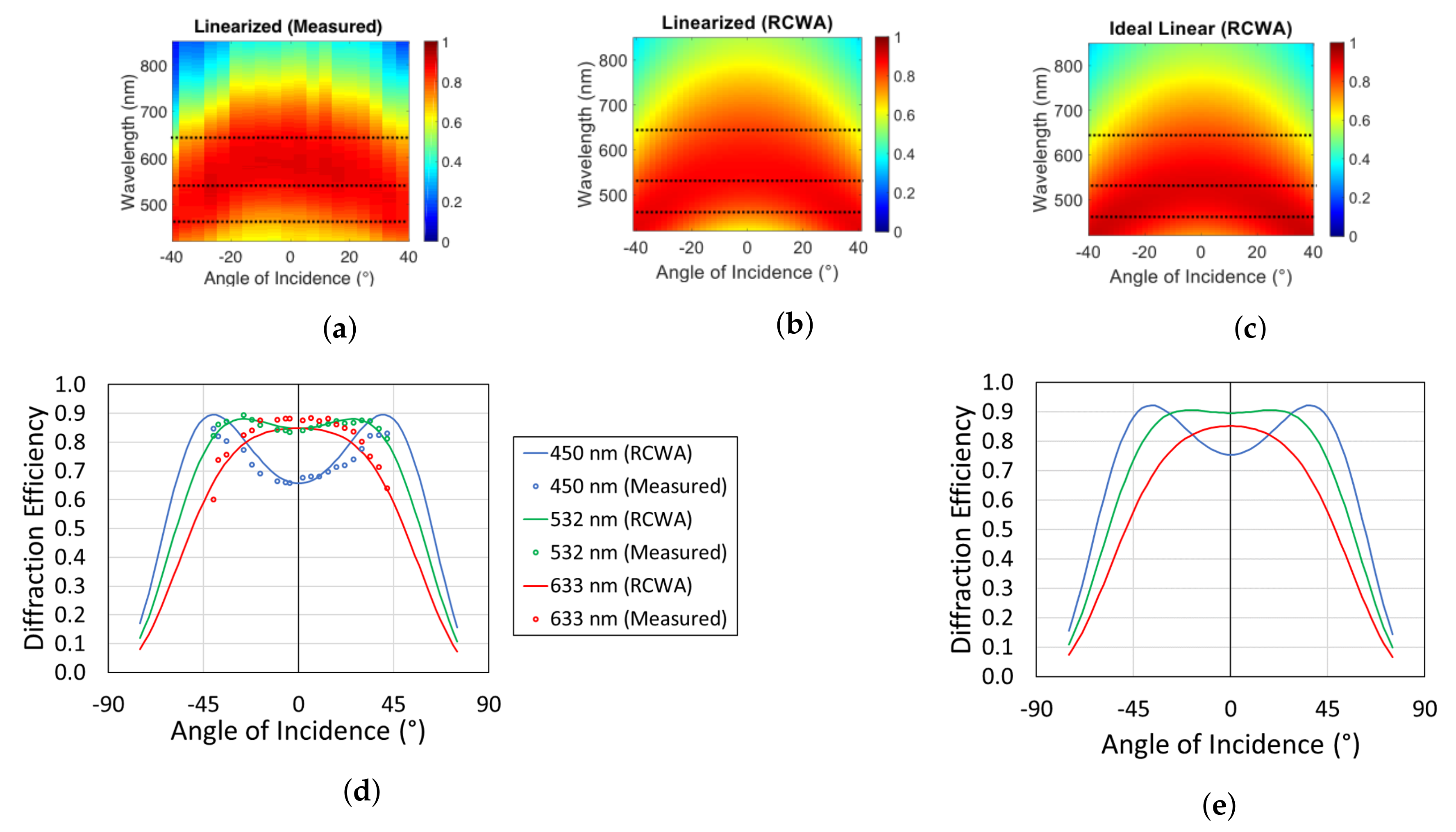
To evaluate the impact of phase state linearity, we can generate a grating using only a subset of the 16 possible phase states. Since the phase distribution is heavily sampled for lower displacements, we can omit some levels and duplicate some of the higher displacement states to map the phase levels closer to the ideal linear ramp (Figure 1c). Using this modified distribution of states, the grating uses 12 of the 16 states and maintains the same period as before. The linearity of the phase distribution is increased from = 0.93 to = 0.99. The measured and simulated efficiencies, compared in Figure 6, approach the expected values for the ideal linear case.
Replacing four of the phase levels in the full 16-level pattern results in a significant increase in the diffraction efficiency by 15.0% (from 69.4% to 84.4%) at 532 nm. Across the entire visible spectrum, the behavior is similar to the non-linear case, but with increased magnitude of efficiency.
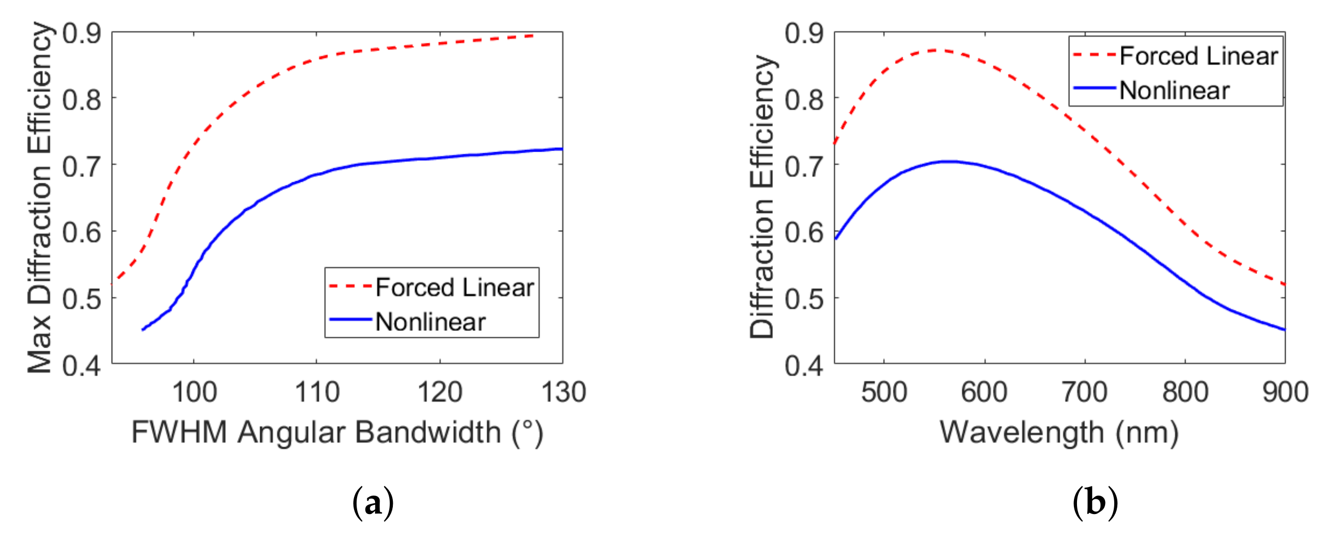
The relationship between the peak diffraction efficiency and the full-width half-maximum (FWHM) angular bandwidth is shown in Figure 7a for the nonlinear and forced linear phase profiles. At any given angular bandwidth, the linearized profile performs significantly better with respect to diffraction efficiency. Similarly, for the spectral response presented in Figure 7b, there is a large drop in efficiency and no significant broadening of the spectral bandwidth. With no angular or spectral benefits provided by the nonlinear profile, the most linear profile (maximum ) is the optimal profile for the blazed grating (i.e., the one with the highest diffraction efficiency) even if it contains fewer unique phase levels.
4.2. Alternative Phase Distributions
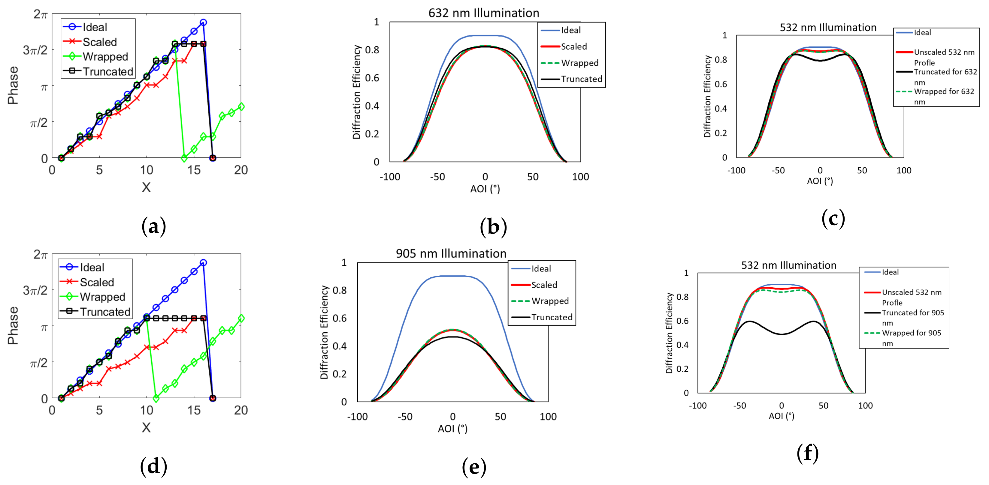
When illuminating a blazed grating (Figure 1) at longer wavelengths, the phase profile is effectively scaled due to the decrease in optical path length for the longer wavelength. The resulting profile has a new blaze angle. To recreate the blaze angle of device at the nominal wavelength, the form of the relative phase profile is scaled for a given wavelength and mapped to the available phase states. Extra phase levels not used to map the scaled profile are truncated to maintain the grating period. This is shown in Figure 8 for 632 nm and 905 nm illumination.
The truncated profile at 632 nm uses two fewer phase levels than the profile for the nominal wavelength (532 nm). The diffraction efficiency profile is decreased by 2% at the peak and is slightly broadened. Similar behavior is seen at 905 nm, but the decrease in efficiency is more significant (6.4%) because the number of truncated phase levels was increased to six. As more phase levels are truncated, the effective fill factor is reduced.
When the new truncated profiles are illuminated with the nominal wavelength, the device is no longer optimized and the diffraction efficiency at normal incidence is reduced by 9.6% at 632 nm and 40.4% at 905 nm, as seen in Figure 8c,f.
With the truncated phase profile, the diffraction angle remains consistent with what is expected from the grating equation. For the case of a period of 16 mirrors at 905 nm, the diffraction angle is 0.30°. The diffraction angle does change when the truncated phase profile is wrapped due to a change in the grating period. Wrapping the truncated phase profile recovers the diffraction efficiency and blaze angle of the original profile but increases the diffraction angle from 0.21° to 0.26° for 632 nm and from 0.30° to 0.48° for 905 nm.
The high diffraction efficiency of 89% gives this PLM an advantage over traditional DMD based SLMs that could only have 10% efficiency. The PLM is also capable of the same tens of kHz refresh rate as the DMD, which will be an advantage over LCoS SLMs that are limited to hundreds of Hz for nematic and a few kHz for ferroelectric [14]. Advances in dual frequency liquid crystal (DFLC) materials have overcome the slow relaxation time of traditional liquid crystals using materials with positive and negative dielectric anisotropy depending on the frequency of the AC bias signal [15]. Using DFLCs, response times have been reduced to submilliseconds, but still only support switching speeds of a few kHz and require two separate AC frequencies to drive [16,17].
Other emerging solutions to the slow response time of LCoS devices typically involve a combination of novel liquid crystal materials and/or metamaterials. Speeds up to 170 kHz have been achieved using solid-state nanoresonator arrays, but spectral bandwidth is limited to near resonance wavelengths and are often unable to provide full wave modulation [18,19,20]. Stressed liquid crystal cells have been demonstrated with speeds passing 10 kHz, but require a large driving voltage [21]. Stressed liquid crystals have not received much traction, likely due to the sensitivity of the manufacturing process [22]. While the PLM requires a complex fabrication process, it has been built on well-established techniques and processes used for commercial DMDs for decades.
5. Conclusions
The diffraction efficiency of a MEMS-based PLM with a nonlinear distribution of addressable phase levels was characterized for a blazed grating. The nonlinear distribution of phase levels has a strong impact on the diffraction efficiency, which can be mitigated to an extent by the how the ideal phase levels are mapped to the addressable states. When linearized, the diffraction efficiency of the PLM increased by 15% for the nominal wavelength.
At the tuned wavelength, the diffraction efficiency is maximum for a broad range of incidence angles in between [−45°, +45°]. This is a suitable range for most projection-based displays and could be improved for applications requiring large field of views by cascading multiple devices. Additionally, increasing the mirror displacement range would be an effective strategy to increase the diffraction at longer wavelengths, such as the communication c-band, 1550 nm, and larger angles of incidence. As the wavelength increases above the tuned wavelength, the phase is under-modulated and the diffraction efficiency becomes narrower across angles of incidence. As the wavelength increases further, the peak efficiency decreases. On the other hand, when the wavelength is decreased below the tuned wavelength, the phase is overmodulated (>2), and the peak diffraction efficiency shifts away from normal incidence. The further away from the tuned wavelength, the further the peaks shift. At 450 nm, the diffraction efficiency peaks are at ±41° with a peak-to-valley of 18%.
For wavelengths that are larger than the maximum mirror displacement, we also demonstrated that it is more favorable to scale the blaze profile—reducing the blaze angle but keeping the grating pitch, rather than to truncate or to wrap the profile (keeping the blaze angle but changing the grating profile).
Supplementary Materials
The following are available online at https://0-www-mdpi-com.brum.beds.ac.uk/2304-6732/8/3/62/s1.
Author Contributions
Data curation, R.S.K.; Investigation, R.S.K.; Project administration, P.-A.B.; Supervision, P.-A.B.; Writing—original draft, R.S.K.; Writing—review & editing, P.-A.B. All authors have read and agreed to the published version of the manuscript.
Funding
This work is supported by Semiconductor Research Corporation Task No. 2810.052 through UT Dallas’ Texas Analog Center of Excellence (TxACE), with Texas Instruments as primary sponsor and industrial liaison.
Data Availability Statement
The data presented in this study is available in supplementary material.
Conflicts of Interest
The authors declare no conflict of interest.
Abbreviations
The following abbreviations are used in this manuscript:
| DFLC | Dual Frequency Liquid Crystal |
| MEMS | Micro-Electromechanical Systems |
| PLM | Phase-only Spatial Light Modulator |
| RCWA | Rigorous Coupled Wave Analysis |
| SEM | Scanning Electron Microscope |
| SLM | Spatial Light Modulator |
| LCoS | Liquid Crystal on Silicon |
| DMD | Digital Micromirror Device |
References
- Yang, D.K.; Wu, S.T. Fundamentals of Liquid Crystal Devices; Lowe, A.C., Sage, I., Eds.; John Wiley & Sons: New York, NY, USA, 2006. [Google Scholar]
- Wang, Y.; Zhou, G.; Zhang, X.; Kwon, K.; Blanche, P.A.; Triesault, N.; Wu, M.C. 2D broadband beamsteering with large-scale MEMS optical phased array. Optica 2019, 6, 557–562. [Google Scholar] [CrossRef] [Green Version]
- Hornbeck, L.J. Digital Light Processing for high-brightness high-resolution applications. In Proceedings of the SPIE 3013 Projection Displays III, San Jose, CA, USA, 8 May 1997. [Google Scholar]
- Blanche, P.-A. (Ed.) Introduction to Holographic Principles. Optical Holography; Elsevier: Amsterdam, The Netherlands, 2020; Chapter 1; pp. 1–39. [Google Scholar]
- Blanche, P.-A.; LaComb, L.; Wang, Y.; Wu, M.C. Diffraction-Based Optical Switching with MEMS. Appl. Sci. 2017, 7, 411. [Google Scholar] [CrossRef] [Green Version]
- Bartlett, T.A.; McDonald, W.C.; Hall, J.N. Adapting Texas Instruments DLP technology to demonstrate a phase spatial light modulator. In Proceedings of the SPIE 10932—Emerging Digital Micromirror Device Based Systems and Applications XI, San Francisco, CA, USA, 4 March 2019; p. 109320S. [Google Scholar]
- Takashima, Y.; Hellman, B.; Rodriguez, J.; Chen, G.; Smith, B.; Gin, A.; Kim, D. MEMS-based Imaging LIDAR. In Optics and Photonics for Energy and the Environment 2018; Optical Society of America: Washington, DC, USA, 2018. [Google Scholar]
- Lee, B.; Yoo, D.; Jeong, J.; Lee, S.; Lee, D.; Lee, B. Wide-angle speckleless DMD holographic display using structured illumination with temporal multiplexing. Opt. Lett. 2020, 45, 2148–2151. [Google Scholar] [CrossRef] [PubMed]
- Gong, Y.; Yang, S.; Gang, K.; Chen, J.; Li, K.; Li, Q. Research on the Fringing-Field Effect of LCoS Devices with Opposite Pretilt Angles for Adjacent Pixels. In Proceedings of the 2019 3rd International Conference on Circuits, System and Simulation (ICCSS), Nanjing, China, 13–15 June 2019; pp. 79–83. [Google Scholar]
- Jung, I.W.; Wang, J.-S.; Solgaard, O. Optical Pattern Generation Using a Spatial Light Modulator for Maskless Lithography. IEEE J. Sel. Top. Quantum Electron. 2007, 13, 147–154. [Google Scholar] [CrossRef]
- López, D.; Aksyuk, V.A.; Watson, G.P.; Mansfield, W.M.; Cirelli, R.; Klemens, F.; Gates, J. Two-dimensional MEMS array for maskless lithography and wavefront modulation. In Proceedings of the SPIE 6589 Smart Sensors, Actuators, and MEMS III, Maspalomas, Spain, 15 May 2007; p. 65890S. [Google Scholar]
- He, Z.; Sui, X.; Jin, G.; Cao, L. Progress in virtual reality and augmented reality based on holographic display. Appl. Opt. 2019, 58, A74–A81. [Google Scholar] [CrossRef] [PubMed]
- Rsoft Photonics Suite. Available online: https://www.synopsys.com/optical-solutions/rsoft.html (accessed on 31 August 2020).
- Zhang, Z.; You, Z.; Chu, D. Fundamentals of phase-only liquid crystal on silicon (LCOS) devices. Light Sci. Appl. 2014, 3, 1–10. [Google Scholar] [CrossRef]
- Xianyu, H.; Wu, S.T.; Lin, C.L. Dual frequency liquid crystals: A review, Liquid Crystals. Liq. Cryst. 2009, 36, 717–726. [Google Scholar] [CrossRef]
- Kowerdziej, R.; Wrobel, J.; Kula, P. Ultrafast electrical switching of nanostructured metadevice with dual-frequency liquid crystal. Sci. Rep. 2019, 9, 20367. [Google Scholar] [CrossRef] [PubMed] [Green Version]
- Lin, X.W.; Hu, W.; Hu, X.K.; Liang, X.; Chen, Y.; Cui, H.Q.; Lu, Y.Q. Fast response dual-frequency liquid crystal switch with photo-patterned alignments. Opt. Lett. 2012, 37, 3627–3629. [Google Scholar] [CrossRef] [PubMed]
- Horie, Y.; Arbabi, A.; Arbabi, E.; Kamali, S.M.; Faraon, A. High-Speed, Phase-Dominant Spatial Light Modulation with Silicon-Based Active Resonant Antennas. Acs Photonics 2018, 5, 1711–1717. [Google Scholar] [CrossRef] [Green Version]
- Park, J.; Jeong, B.G.; Kim, S.I.; Lee, D.; Kim, J.; Shin, C.; Choi, B.L. All-solid-state spatial light modulator with independent phase and amplitude control for three-dimensional LiDAR applications. Nat. Nanotechnol. 2021, 16, 69–76. [Google Scholar] [CrossRef] [PubMed]
- Sherrott, M.C.; Hon, P.W.; Fountaine, K.T.; Garcia, J.C.; Ponti, S.M.; Brar, V.W.; Atwater, H.A. Experimental Demonstration of >230° Phase Modulation in Gate Tunable Graphene-Gold Reconfigurable Mid-Infrared Metasurfaces. Nano Lett. 2017, 17, 3027–3034. [Google Scholar] [CrossRef] [PubMed] [Green Version]
- Wang, B.; Zhang, G.; Glushchenko, A.; West, J.L.; Bos, P.J.; McManamon, P.F. Stressed liquid-crystal optical phased array for fast tip-tilt wavefront correction. Appl. Opt. 2017, 44, 7754–7759. [Google Scholar] [CrossRef] [PubMed]
- Melnyk, O.; Garbovskiy, Y.; Glushchenko, A. Science and technology of stressed liquid crystals: Display and non-display applications. Phase Transit. 2017, 90, 773–779. [Google Scholar] [CrossRef]
Figure 1.
Phase profiles for one period of: (a) A linear distribution of phase levels, (b) non-linear (all 16 available phase levels on the device), and (c) a forced linear distribution of phase levels mapped to the available states of the device when illuminated with a 532 nm laser.
Figure 1.
Phase profiles for one period of: (a) A linear distribution of phase levels, (b) non-linear (all 16 available phase levels on the device), and (c) a forced linear distribution of phase levels mapped to the available states of the device when illuminated with a 532 nm laser.

Figure 2.
First-order diffraction efficiency for multistep blazed gratings. Nonlinear phase levels below N = 16 were chosen from the available levels such that the phase profile followed the same trend as the device being tested and had similar values.
Figure 2.
First-order diffraction efficiency for multistep blazed gratings. Nonlinear phase levels below N = 16 were chosen from the available levels such that the phase profile followed the same trend as the device being tested and had similar values.

Figure 3.
Experimental setup for measuring the diffraction efficiency across the visible spectrum.

Figure 4.
(a) Phase-only spatial light modulator (PLM) in housing and (b) scanning electron microscope (SEM) image of individual mirrors (courtesy of Texas Instruments).
Figure 4.
(a) Phase-only spatial light modulator (PLM) in housing and (b) scanning electron microscope (SEM) image of individual mirrors (courtesy of Texas Instruments).

Figure 5.
Diffraction efficiency for a blazed grating using all available phase levels. (a) Measured diffraction efficiencies for a 16-state blazed grating, (b) rigorous coupled wave analysis (RCWA) simulations (dashed lines correspond to common laser lines at 450 nm, 532 nm, and 632.8 nm), and (c) cross-sections of measured and simulated diffraction efficiencies for 450 nm, 532 nm, and 632.8 nm.

Figure 6.
(a) Measured diffraction efficiencies for a 16-state blazed grating, (b) RCW-simulated, and (c) ideal linear phase distribution. Dashed lines correspond to common laser lines at 450 nm, and 632.8 nm shown in (d) for linearized PLM phase levels and (e) an ideal linear 16-level grating.
Figure 6.
(a) Measured diffraction efficiencies for a 16-state blazed grating, (b) RCW-simulated, and (c) ideal linear phase distribution. Dashed lines correspond to common laser lines at 450 nm, and 632.8 nm shown in (d) for linearized PLM phase levels and (e) an ideal linear 16-level grating.

Figure 7.
Diffraction efficiency for linearized and nonlinear phase profiles with respect to (a) angular bandwidth, and (b) wavelength at normal incidence.
Figure 7.
Diffraction efficiency for linearized and nonlinear phase profiles with respect to (a) angular bandwidth, and (b) wavelength at normal incidence.

Figure 8.
(a) Scaled, truncated, and wrapped phase profiles modified for a 632 nm operating wavelength, (b) simulated diffraction efficiency for phase profiles modified for 632 nm operating wavelength, (c) simulated diffraction efficiency for phase profiles modified for a 632 nm operating wavelength illuminated at 532 nm, (d) modified phase profiles dor 905 nm operating wavelength, (e) simulated diffraction efficiency for phase profiles modified for a 905 nm operating wavelength, and (f) simulated diffraction efficiency for phase profiles modified for a 905 nm operating wavelength illuminated at 532 nm.

Publisher’s Note: MDPI stays neutral with regard to jurisdictional claims in published maps and institutional affiliations. |
© 2021 by the authors. Licensee MDPI, Basel, Switzerland. This article is an open access article distributed under the terms and conditions of the Creative Commons Attribution (CC BY) license (http://creativecommons.org/licenses/by/4.0/).
Share and Cite
MDPI and ACS Style
Ketchum, R.S.; Blanche, P.-A. Diffraction Efficiency Characteristics for MEMS-Based Phase-Only Spatial Light Modulator with Nonlinear Phase Distribution. Photonics 2021, 8, 62. https://0-doi-org.brum.beds.ac.uk/10.3390/photonics8030062
AMA Style
Ketchum RS, Blanche P-A. Diffraction Efficiency Characteristics for MEMS-Based Phase-Only Spatial Light Modulator with Nonlinear Phase Distribution. Photonics. 2021; 8(3):62. https://0-doi-org.brum.beds.ac.uk/10.3390/photonics8030062
Chicago/Turabian StyleKetchum, Remington S., and Pierre-Alexandre Blanche. 2021. "Diffraction Efficiency Characteristics for MEMS-Based Phase-Only Spatial Light Modulator with Nonlinear Phase Distribution" Photonics 8, no. 3: 62. https://0-doi-org.brum.beds.ac.uk/10.3390/photonics8030062
Note that from the first issue of 2016, this journal uses article numbers instead of page numbers. See further details here.