Development of Micron Sized Photonic Devices Based on Deep GaN Etching


1
Institute of Electronics, Université Polytechnique Hauts de France, Microelectronics & Nanotechnology IEMN CNRS UMR 8520, 59313 Valenciennes, France
2
TMO Transformation Management Office, Riyad 11564, Saudi Arabia
3
Centre for Nanoscience and Nanotechnology (C2N), CNRS, UMR 9001, 91460 Marcoussis, France
*
Author to whom correspondence should be addressed.
Photonics 2021, 8(3), 68; https://0-doi-org.brum.beds.ac.uk/10.3390/photonics8030068
Submission received: 27 December 2020
/
Revised: 18 February 2021
/
Accepted: 27 February 2021
/
Published: 2 March 2021
(This article belongs to the Special Issue Wide Bandgap Semiconductor Photonic Devices)
Abstract
:In order to design and development efficient III-nitride based optoelectronic devices, technological processes require a major effort. We propose here a detailed review focussing on the etching procedure as a key step for enabling high date rate performances. In our reported research activity, dry etching of an InGaN/GaN heterogeneous structure was investigated by using an inductively coupled plasma reactive ion etching (ICP-RIE). We considered different combinations of etch mask (Ni, SiO2, resist), focussing on the optimization of the deep etching process. A GaN mesa process with an etching depth up to 6 µm was performed in Cl2/Ar-based plasmas using ICP reactors for LEDs dimen sions ranging from 5 to 150 µm². Our strategy was directed toward the mesa formation for vertical-type diode applications, where etch depths are relatively large. Etch characteristics were studied as a function of ICP parameters (RF power, chamber pressure, fixed total flow rate). Surface morphology, etch rates and sidewall profiles observed into InGaN/GaN structures were compared under different types of etching masks. For deep etching up to few microns into the GaN template, we state that a Ni or SiO2 mask is more suitable to obtain a good selectivity and vertical etch profiles. The optimized etch rate was about 200nm/min under moderate ICP conditions. We applied these conditions for the fabrication of micro/nano LEDs dedicated to LiFi applications.
1. Introduction
GaN and related alloys are among the most attractive materials, due to their excellent characteristics as well as large bandgap, high breakdown electrical field and high electron saturation velocity, for applications such light emitting diodes (LEDs), lasers, photodetectors and high power electronics [1,2,3,4,5,6]. Mature material associated with optimized technological processes is the key issue for the near future development of active/passive RF-optoelectronic components. Dry etching processes dedicated to ternary structures (such as InxGa1−xN and GaN) are of particular importance, since such devices generally include heterostructures. Hence, the fabrication of GaN-based optoelectronic devices depends on dry etching either partially or totally. Typically, the etch process should yield high etch rates, minimal surface roughening, good reproducibility and a high degree of anisotropy. All of these properties can be achieved with inductively coupled plasma (ICP) etching Sidewall and etched surface morphology are critical parameters in the formation of mesas or vertical devices with high ratio aspect. In the actual context of photonic devices, requirements for GaN etching are fixed in the order of few hundred nanometers [7,8,9], whereas this is completely different for those expected for vertical power devices [10,11,12]. Deep etching of GaN is presently needed for new applications such as photonic, power and microelectromechanical system devices for device isolation, waveguide or vertical channel formation [13,14,15]. Low etch depth has been successfully employed for InGaN/GaN devices to create photonics crystal and LED mesas with, in general, etch depths below 1um, while deep etch has been mainly focused on GaN materials and not actual devices. Hence more work is required to apply and optimize deep etch to create functional devices [16,17,18] The approach is to etch the epilayer from p-type GaN to sapphire to form individual or interconnected microchips for a micro-LED array [19]). Our purpose is to have a chip-to-chip isolation and to improve the electrical performance by reducing the metal surface and global capacitance induced by metallization contacts (pads, connection line) on n-GaN. The deep etching process was performed to define independent mesa. Different configurations of etching masks were defined. Photoresist (AZ9260), metal (Ni) and silicon dioxide (SiO2) were used as etching masks. The objective was to assess surface morphology, mesa edges and the etching sidewall quality. Several dimensions of etched mesas ranging from 5 × 5 to 150 × 150 µm² were evaluated as a function of etching profile. The effect of different masks on the etched mesa are discussed for depths varying from hundreds of nanometers up to a few micrometers. We also illustrated the effects of etched parameters on the resulting characteristics, such as etch rate, mask erosion and, as a consequence, surface roughness.
2. Experimental Details
In our investigation, III-Nitride layers were grown by NovaGaN Ltd. (Lausanne, Switzerland), using a metalorganic chemical vapour deposition system (MOCVD) on c-face sapphire substrates. The epilayer structure consisted of 2 µm thick undoped GaN, 1 µm thick n-GaN, ten periods of 10 nm thick GaN/3 nm thick InGaN MQW and 100 nm thick p-GaN (as shown in Figure 1a,b). Cross-sections and plan-views of the samples were investigated by high-angle annular dark field scanning transmission electron microscopy (HAADF-STEM). Samples were prepared by tilting along the (1100) and (1120) axes on thin foils by Focused Ion Beam (FIB) in order to see the dislocations, chemical analysis and stacking faults. Pinching zones generate threading dislocations (yellow arrows) associated with plastic relaxation mechanism. They also lead to variation of the top layer thickness (p-GaN layer) above these zones. Our investigations revealed that InGaN/GaN samples had threading dislocation densities in the range of 3–5 × 108 cm−2. Dislocations were created during growth due to the lattice mismatch between the sapphire substrate and GaN [20,21,22]. Usually, the Cl2/Ar based plasma shows correct results such as high etch rates, anisotropic profile and a smooth surface of homogeneous GaN [23,24].
For the formation of the etching mask, we considered three possible combinations: photoresist (4 μm thick AZ9260), SiO2 and Ni layers with a thickness of 600 nm and 520 nm, respectively. The latter were deposited by RF sputtering on p-GaN/InGaN/n-GaN. Patterning was realized by a lift-off process. Dry etching was performed using an Oxford plasmalab 100 plus system. Samples (1.5 × 2 cm) were mounted on a three inches Si wafer using a thermally conductive paste and loaded on the wafer carrier. The temperature of the backside cooled sample chuck was kept at 10 °C.
Using Ni, SiO2 and photoresist masks, the etching conditions were 10 sccm of Cl2, 30 sccm of Ar, 10 mTorr total pressure and ICP power ranging from 100 to 500 Watts. The ICP power and, indirectly, high-density plasma were limited to 500W in order to avoid damage to the masking material and etching selectivity. Etch depths were obtained from surface profilometer measurements after mask removal. The surface morphology was examined using SEM.
3. Results and Discussion
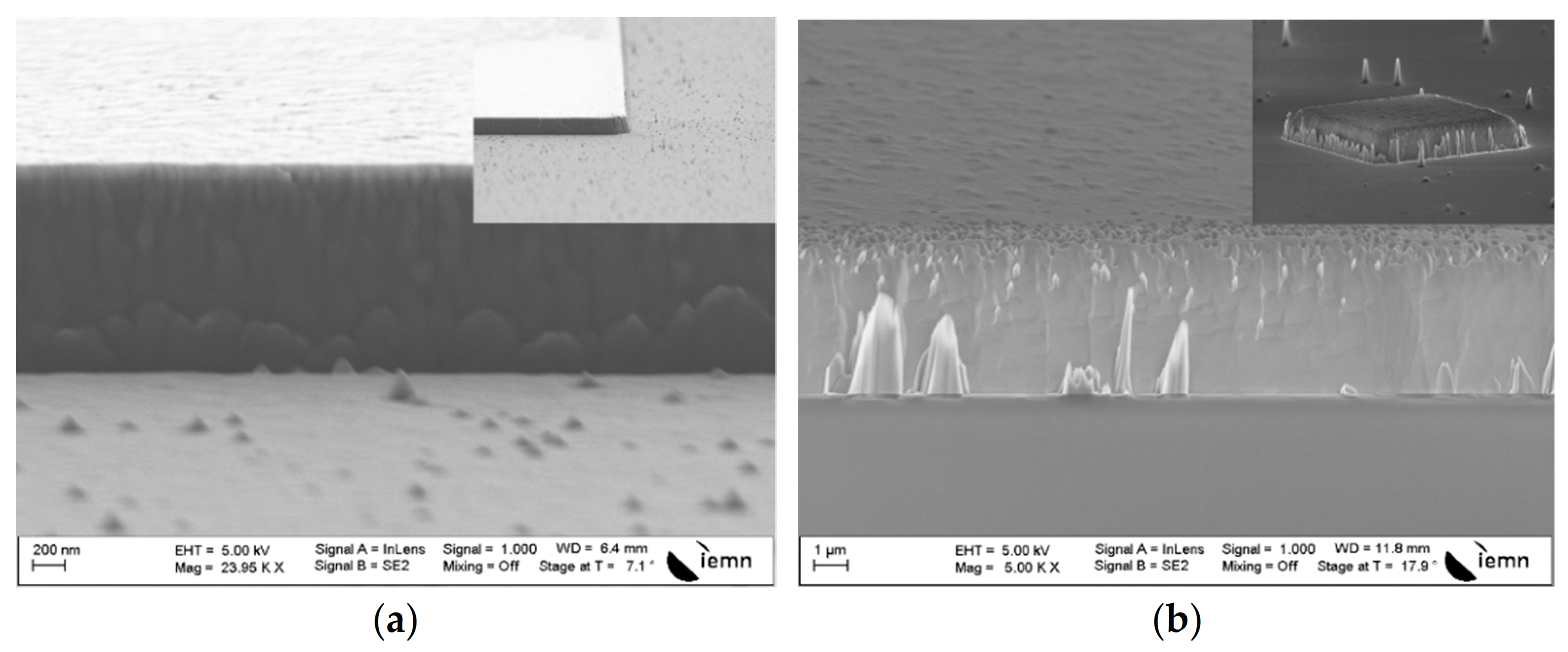
A first section of the p-GaN/InGaN/n-GaN MQW template was initially etched in order to attain the n-type GaN layer. This resulted in a 3 µm depth mesa, as described in Figure 2a,b, under the same conditions described above. After this, we applied Cl2/Ar plasma to etch the last section of the template, the 100 nm thick p-GaN layer. During chlorination of GaN, chlorine preferentially reacts with the gallium species (Ga) surface atoms to form Ga chlorides. For etching of the InGaN/GaN MQW layered structure, the indium species (In) is involved in the chemical reaction and contributes to the formation of In chloride on surface [25], which is not volatile at the process temperature. A hard mask, such as nickel (Ni), is preferred for photoresist because etch selectivity of GaN over photoresist is more advantageous in Cl2-based plasma chemistry. The best etching surface profile is also obtained using an Ni mask compared to those for SiO2 or photoresist masks. GaN etch rates and the selectivity over etch mask were evaluated from the depth of the etched measured by the profilometry. We noticed that a selectivity of 17 was found for the Ni mask, which is much higher than 5.3 and 1.5 for, respectively, SiO2 and photoresist masks as detailed above. Using an ICP power of 500 Watts and RF power of 100 Watts for each Ni, SiO2 and photoresist mask, the resulting etched surface profiles are shown in Figure 2a,b. The surface morphology revealed a more homogenous and smoother aspect when the Ni mask was selected.
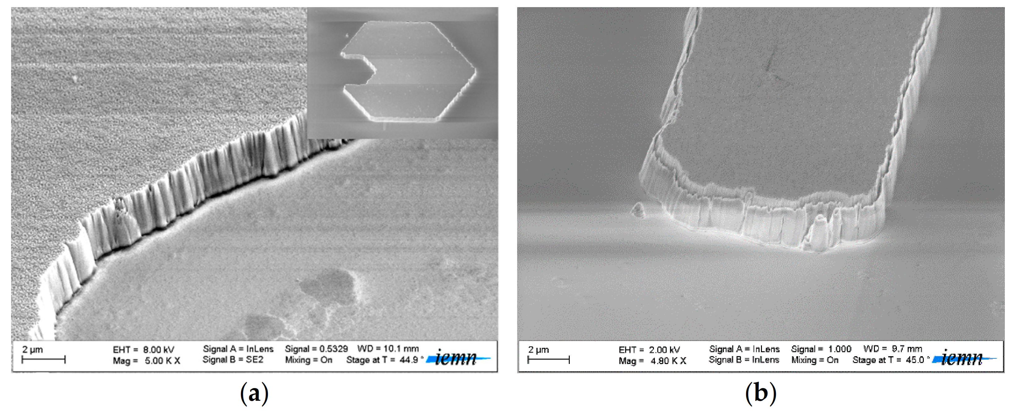
We applied a deep etching procedure in order to analyze the maximal endurance and the toughness of the SiO2 mask. As shown in Figure 3a, the quality of etching mesa was satisfactory for mesa size larger than 20 × 20 µm2 but limited quality was obtained for mesa below this dimension. Damaged areas were observed in the border to mesa indicating the limitation of the SiO2 etching mask. The formation of columnar defects also appeared using the SiO2 cover-plate in this range of etching profile. Columnar defects are generally due to a micromasking effect [26]. They originate from sputtering of hard mask materials, which deposit particles on the etched surface and create a local micromask: Figure 3b shows an etched GaN mesa with an SiO2 cover plate. The etched surface presented a regular morphology but with the presence of GaN spikes with diameters from 50 to 200 nm, and heights from 1 to 2 μm, at certain places of the etched surface.
In order to etch entirely the epilayer through the etch mask to expose the sapphire substrate, high ion fluxes were required to achieve high etch rate for the formation of a thick mesa. In addition, high ICP power (>500 Watts) could result in extensive roughness on the sidewall due to mask damage or erosion during etching. The use of an Ni mask allowed reduction of erosion of the mask edge and limited the formation of pillars observed when using an oxide mask. The SiO2 mask erosion could be delayed by increasing the thickness of the etch mask. The presence of nonuniformity on the SiO2 mask shape could cause damage or striations to the sidewalls of the etched sample. These irregularities on the mask boundaries could be reduced by optimizing the lithography process used to pattern the SiO2. We investigated the experiment with a SiO2 mask of 600 nm thickness, using GaN epilayers grown thicker on a sapphire substrate. The SiO2 mask seemed to be a good choice for the mask because it offered sidewalls with reduced roughness and correct selectivity. The mesa sidewall as shown Figure 3b, had a profile with a lower slope, which was acceptable for a deep etch close to 4.5 µm. Compared to the Ni mask, higher ICP powers sputtered the SiO2 mask faster and caused the redeposition of residues on the surface which created a more columnar defect due to micromasking during the etch. During etching of the InGaN/GaN by Cl2/Ar plasma, low volatile In chlorides can be formed on the etched surface [27]. In could be involved in the plasma reaction with chlorine and favorable to the pillar’s formation [28] by the micro-masks on the etch surface. Moreover, part of pillars results from structural defects and dislocations in GaN. When the etch depth increases, the density of these surface features was found to increase. When the etch depth was less than 2 µm, there was nearly no pillars observed on the etched GaN surface. Although a number of studies have been performed on the plasma etching of GaN, very little is known about the mechanism of pillar or pit formation on the etched surface of the GaN/InGaN heterostructure [29].
Let us consider now the third option with application of a photoresist mask. Etching conditions were 10 sccm of Cl2, 30 sccm of Ar, 10 mTorr total pressure and 500 Watts ICP power. AZ9260 Photoresist used as etching mask exhibited poor persistence to the ICP etching process. Photoresist etch masks have a low selectivity compared to GaN [30]. A hard masks such as Ni is preferred for photoresist because etch selectivity of GaN over photoresist is more advantageous in Cl2-based plasma chemistry. We observed that GaN etching occurs without any pattern deformation at low ICP power (150 Watts) and moderate etch rates within the same conditions. Up to this power value, the photoresist mask is drastically affected by mask damage and edge degradations. Figure 4a shows the etched mesa with an optimized depth obtained at 1.5 µm for larger dimensions (from 50 to 200 µm2). Concerning mesa sizes smaller than 10 µm², the etching process was limited in terms of quality and shape, showing defective areas in the mesa edges as illustrated in Figure 4b. The photoresist mask was a material less robust and more affected with physical bombardment contribution.
The Ni mask represents the best choice for obtaining a high-selectivity and vertical etch profiles for deep etched structures. Throughout the experiment, RF power, ratio of mixed gas and chamber pressure were conserved, which seems to be a good compromise for high etching rate and to investigate the impact of ICP power on the etched profile and nature of masks. The temperature of the backside cooled sample chuck was maintained at 10 °C. We therefore studied the etch rate as a function of ICP power. Further experiments using different gas combinations will be investigated for improvements, while focusing on one mask.
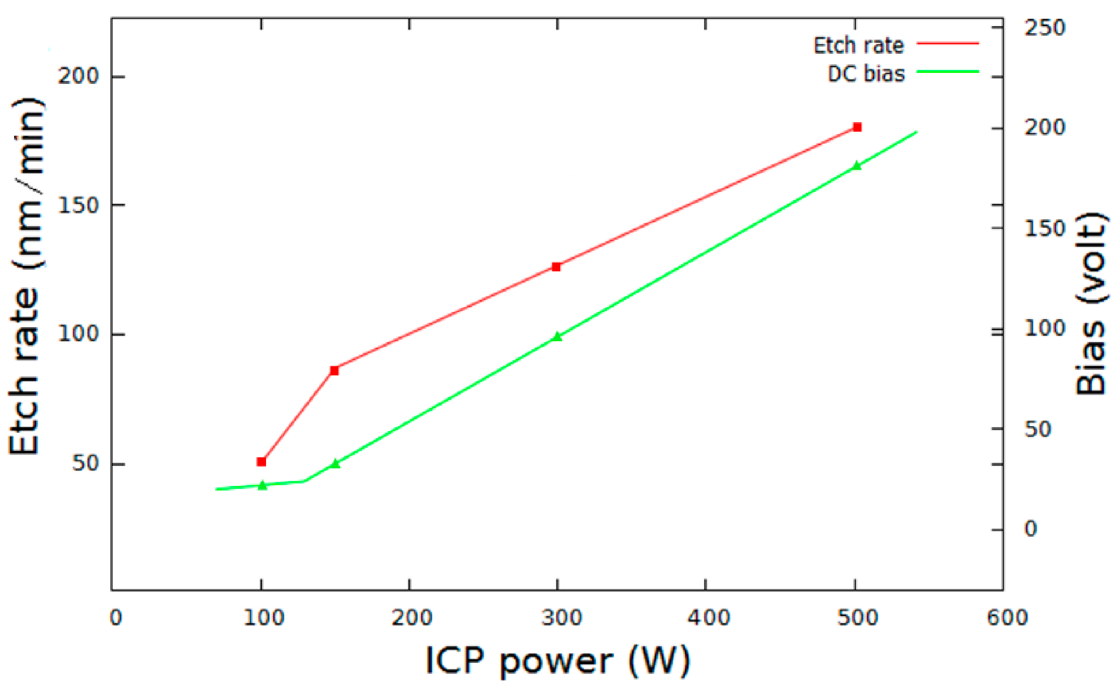
Ni masks permitted us to study the ICP power parameter, demonstrating a key element in the etching rate. The different values used in this experiment led to extracting different etching conditions. Increasing the ICP power led to increasing chemical component of the etch flow at identical conditions. Figure 5 shows the linear influence on the etch rate and the DC bias when increasing the ICP power. We observed that a compromise was found for a very low inclination and smooth sidewall mesa for the Ni mask when ICP power was 500 Watts with an etch rate of 198 nm/min.
4. Conclusions
Dry etching of p-GaN/InGaN/n-GaN structures was carried out in Cl2/Ar inductively coupled plasmas. The objective was directed toward mesa formation for vertical-type devices, where the etch depth is up to 3 µm. Through a combination of etch masks and the plasma etch process, mesa structures with smooth sidewalls and reduced post-etch residues were achieved. In our investigations, dry etch development was focused on deep mesa into GaN materials. The etch parameters were adjusted to obtain high etch depth with low defects and good verticality. The experiment indicated that the Ni mask is more appropriate for the deep etch process in comparison to SiO2 and photoresist masks in the case of micro-mesa etching. Such a mask is more suitable to obtain a good selectivity and vertical etch profiles for an etch depth exceeding 6μm. The highest etch rate was 198 nm/min at ICP power of 500 Watts. Here we found that the most vertical and smooth sidewall mesa were produced for the higher ICP power. We observed an increase in the etch rate of GaN with increasing ICP power attributed to increase in Cl radical and ion density in the plasma. The pattern transfer during etching was intimately limited by the quality of the etch mask and an inappropriate mask could result in surface morphologies that include pits and/or pillars. ICP etching can potentially provide relatively low damage while maintaining fast etching rates and superior uniformity with an Ni mask. The nature of etching masks also plays an important role in device performance due their junction and possible contamination of sidewalls during etching process. Subsequently, the evaluation of electrical response is largely impacted by the nature and the quality of the etching process.
Author Contributions
K.D. and B.A. designed the masks for clean room experiment and performed the etching process. G.P. performed the TEM characterizations. E.D. wrote the manuscript. All authors have read and agreed to the published version of the manuscript.
Funding
This work was funded by the Bureau Culturel Saoudien-Ambassade d’Arabie Saoudite, Paris, France.
Data Availability Statement
The data presented in this study are available on request from the corresponding author.
Acknowledgments
We acknowledge the support from the Saudi Cultural Attaché, Bureau Culturel Saoudien, Ambassade d’Arabie Saoudite à Paris, France.
Conflicts of Interest
The authors declare no conflict of interest.
References
- Li, X.; Jiang, Y.; Li, J.; Shi, Z.; Zhu, G.; Wang, Y. Integrated photonics chip with InGaN/GaN light-emitting diode and bended waveguide for visible-light communicacations. Opt. Laser Technol. 2019, 114, 103–109. [Google Scholar] [CrossRef]
- Zhou, S.; Wang, S.; Liu, S.; Ding, H. High power GaN-based LEDs with low optical loss electrode structure. Opt. Laser Technol. 2013, 54, 321–325. [Google Scholar] [CrossRef]
- Li, K.H.; Fu, W.Y.; Cheung, Y.F.; Wong, K.K.Y.; Wang, Y.; Lau, K.M.; Choi, H.W. Monolithically integrated InGaN/GaN light-emitting diodes, photodetectors, and waveguides on Si substrate. Optica 2018, 5, 564. [Google Scholar] [CrossRef]
- Nakamura, S. InGaN-Based laser diodes. Annu. Rev. Mater. Sci. 1998, 28, 125–152. [Google Scholar] [CrossRef]
- Omnès, F.; Monroy, E.; Muñoz, E.; Reverchon, J.-L. Wide bandgap UV photodetectors: A short review of devices and applications. SPIE 2007, 6473, 64730E. [Google Scholar]
- Lee, K.H.; Joo, D.H.; Kim, M.S.; Yu, J.S. Improved light extraction of InGaN/GaN blue LEDs by GaOOH NRAs using a thin ATO seed layer. Nanoscale Res. Lett. 2012, 7, 458. [Google Scholar] [CrossRef] [Green Version]
- Khokhar, A.Z.; Parsons, K.; Hubbard, G.; Rahman, F.; Macintyre, D.S.; Xiong, C.; Massoubre, D.; Gong, Z.; Johnson, N.P.; De La Rue, R.M.; et al. Nanofabrication of gallium nitride photonic crystal light-emitting diodes. Microelectron. Eng. 2010, 87, 2200–2207. [Google Scholar] [CrossRef] [Green Version]
- Hong, S.; Cho, C.; Lee, S.; Yim, S.; Lim, W.; Kim, S.; Park, S. Localized surface plasmon-enhanced near-ultraviolet emission from InGaN/GaN light-emitting diodes using silver and platinum nanoparticles. Opt. Express 2013, 21, 3138–3144. [Google Scholar] [CrossRef] [PubMed]
- Baik, K.H.; Pearton, S.J. Dry etching characteristics of GaN for blue/green light-emitting diode fabrication. Appl. Surf. Sci. 2009, 255, 5948–5951. [Google Scholar] [CrossRef]
- Zhang, Y.; Sun, M.; Piedra, D.; Azize, M.; Zhang, X.; Fujishima, T.; Palacios, T. GaN-on-Si vertical schottky and p-n diodes. IEEE Electron. Dev. Lett. 2014, 35, 618–620. [Google Scholar]
- Hu, J.; Zhang, Y.; Sun, M.; Piedra, D.; Chowdhury, N.; Palacios, T. Materials and processing issues in vertical GaN power electronics. Mater. Sci. Semicond. Proc. 2018, 78, 75–84. [Google Scholar] [CrossRef] [Green Version]
- Tohru, O. Recent development of vertical GaN power devices: Japanese. J. Appl. Phys. 2019, 58, SB0805. [Google Scholar]
- Xiao, M.; Yan, X.; Xie, J.; Beam, E.; Cao, Y.; Wang, H.; Zhang, Y. Origin of leakage current in vertical GaN devices with nonplanar regrown p-GaN. Appl. Phys. Lett. 2020, 117, 183502. [Google Scholar] [CrossRef]
- Sun, Y.; Kang, X.; Zheng, Y.; Lu, J.; Tian, X.; Wei, K.; Wu, H.; Wang, W.; Liu, X.; Zhang, G. Review of the Recent Progress on GaN-Based Vertical Power Schottky Barrier Diodes (SBDs). Electronics 2019, 8, 575. [Google Scholar] [CrossRef] [Green Version]
- Hsieh, Y.; Chen, W.; Chang, L.; Chow, L.; Borges, S.; Schulte, J.A.; Huang, S.; Jeng, M.; Yu, C. Etched Gallium Nitride Waveguide for RamanSpectroscopic Applications. Crystals 2019, 9, 176. [Google Scholar] [CrossRef] [Green Version]
- Qiu, R.; Lu, H.; Chen, D.; Zhang, R.; Zheng, Y. Optimization of inductively coupled plasma deep etching of GaN and etching damage analysis. Appl. Surf. Sci. 2011, 257, 2700. [Google Scholar] [CrossRef]
- le Boulbar, E.D.; Lewins, C.J.; Allsopp, D.W.E.; Bowen, C.R.; Shields, P.A. Fabrication of high-aspect ratio GaN nanostructures nanostructures for advanced photonic devices. Microelectron. Eng. 2016, 153, 132–136. [Google Scholar] [CrossRef] [Green Version]
- Okada, N.; Nojima, K.; Ishibashi, N.; Nagatoshi, K.; Itagaki, N.; Inomoto, R.; Motoyama, S.; Kobayashi, T.; Tadatomo, K. Formation of distinctive structures of GaN by inductively-coupled-plasma and reactive ion etching under optimized chemical etching conditions. AIP Adv. 2017, 7, 065111. [Google Scholar] [CrossRef] [Green Version]
- Jeon, C.W.; Choi, H.W.; Dawson, M.D. Fabrication of Matrix-Addressable InGaN-Based Microdisplays of High Array Density. IEEE Photonics Technol. Lett. 2003, 15, 1516–1518. [Google Scholar] [CrossRef]
- Wu, X.H.; Elsass, C.R.; Abare, A.; MacK, M.; Keller, S.; Petroff, P.M.; Denbaars, S.P.; Speck, J.S.; Rosner, S.J. Structural origin of V-defects and correlation with localized excitonic centers in InGaN/GaN multiple quantum wells. Appl. Phys. Lett. 1998, 72, 692–694. [Google Scholar] [CrossRef]
- Lester, S.D.; Ponce, F.A.; Craford, M.G.; Steigerwald, D.A. High dislocation densities in high efficiency GaN-based light-emitting diodes. Appl. Phys. Lett. 1995, 66, 1249–1251. [Google Scholar] [CrossRef]
- Kim, I.H.; Park, H.S.; Park, Y.J.; Kim, T. Formation of V-shaped pits in InGaN/GaN multiquantum wells and bulk InGaN films. Appl. Phys. Lett. 1998, 73, 1634–1636. [Google Scholar] [CrossRef]
- Yang, G.F.; Chen, P.; Wu, Z.L.; Yu, Z.G.; Zhao, H.; Liu, B.; Hua, X.M.; Xie, Z.L.; Xiu, X.Q.; Han, P. Characteristics of GaN thin films by inductively coupled plasma etching with Cl2/BCl3 and Cl2/Ar. J. Mater. Sci. Mater. Electron. 2012, 23, 1224–1228. [Google Scholar] [CrossRef]
- Cho, H.; Hahn, Y.B.; Hays, D.C.; Jung, K.B.; Donovan, S.M.; Abernathy, C.R.; Pearton, S.J.; Shul, R.J. Inductively Coupled Plasma Etching of III-Nitrides in Cl2/Xe, Cl2/Ar and Cl2/He. Mater. Res. Soc. Internet J. Nitride Semicond. Res. 1999, 4, 763–768. [Google Scholar] [CrossRef] [Green Version]
- Rawal, D.; Arora, H.; Sehgal, B.; Muralidharan, R. Comparative study of GaN mesa etch characteristics in Cl2 based inductively coupled plasma with Ar and BCl3 as additive gases. J. Vacuum Sci. Technol. A 2014, 32, 031301. [Google Scholar] [CrossRef]
- Kim, H.K.; Lin, H.; Ra, Y. Etching mechanism of a GaN/InGaN/GaN heterostructure in Cl2 and CH4 based inductively coupled plasmas. J. Vac. Sci. Technol. A 2004, 22, 598–601. [Google Scholar] [CrossRef]
- Lai, Y.; Yeh, C.; Wang, J.; Wang, H.H.; Chen, C.; Hung, W. Sputtering and Etching of GaN Surfaces. J. Phys. Chem. B 2001, 105, 10029–10036. [Google Scholar] [CrossRef]
- Ladroue, J.; Meritan, A.; Boufnichel, M.; Lefaucheux, P.; Ranson, P.; Dussart, R. Deep GaN etching by inductively coupled plasma and induced surface defects. J. Vac. Sci. Technol. A 2010, 28, 1226. [Google Scholar] [CrossRef]
- Evgeny, Z.; Sergei, S.; Alan, G.; Wang, W.N.; Shreter, Y.G.; Tarkhin, D.V.; Bochkareva, N.I. ICP etching of III-nitride based laser structure with Cl2–Ar plasma assisted by Si coverplate material. J. Vac. Sci. Technol. A 2005, 23, 687–692. [Google Scholar]
- Lee, H.; Harris, J. Iron nitride mask and reactive ion etching of GaN films. J. Electron. Mater. 1998, 27, 185–189. [Google Scholar] [CrossRef]
Figure 1.
(a) InGaN/GaN Multi-Quantum Well (MQW) structure layers. (b) Scanning transmission electron microscopy (STEM) cross section along the (1120) zone axis showing dislocations.
Figure 1.
(a) InGaN/GaN Multi-Quantum Well (MQW) structure layers. (b) Scanning transmission electron microscopy (STEM) cross section along the (1120) zone axis showing dislocations.

Figure 2.
(a) Scanning electron microscope (SEM) analysis of mesa sidewalls after inductively coupled plasma (ICP) etching with sputtered nickel mask (depth of 3 µm for ICP power of 500 Watts. (b) Typical etching results showing Ni mask.
Figure 2.
(a) Scanning electron microscope (SEM) analysis of mesa sidewalls after inductively coupled plasma (ICP) etching with sputtered nickel mask (depth of 3 µm for ICP power of 500 Watts. (b) Typical etching results showing Ni mask.

Figure 3.
(a) Cross section SEM images of InGaN/GaN MQW structure after ICP etching with etching depth of 1 µm with SiO2 mask, and (b) observation of mesa sidewall etching with SiO2 mask (Etching depth of 4 µm at 500 Watts ICP power).
Figure 3.
(a) Cross section SEM images of InGaN/GaN MQW structure after ICP etching with etching depth of 1 µm with SiO2 mask, and (b) observation of mesa sidewall etching with SiO2 mask (Etching depth of 4 µm at 500 Watts ICP power).

Figure 4.
SEM images of mesa sidewalls using a photoresist mask: total etching depth of 1.5 µm, with a mesa width of (a) 100 µm and (b) 10 µm -ICP power of 150 Watts.
Figure 4.
SEM images of mesa sidewalls using a photoresist mask: total etching depth of 1.5 µm, with a mesa width of (a) 100 µm and (b) 10 µm -ICP power of 150 Watts.

Figure 5.
Etch rate of GaN and corresponding DC bias versus ICP power.

Publisher’s Note: MDPI stays neutral with regard to jurisdictional claims in published maps and institutional affiliations. |
© 2021 by the authors. Licensee MDPI, Basel, Switzerland. This article is an open access article distributed under the terms and conditions of the Creative Commons Attribution (CC BY) license (http://creativecommons.org/licenses/by/4.0/).
Share and Cite
MDPI and ACS Style
Dogheche, K.; Alshehri, B.; Patriache, G.; Dogheche, E. Development of Micron Sized Photonic Devices Based on Deep GaN Etching. Photonics 2021, 8, 68. https://0-doi-org.brum.beds.ac.uk/10.3390/photonics8030068
AMA Style
Dogheche K, Alshehri B, Patriache G, Dogheche E. Development of Micron Sized Photonic Devices Based on Deep GaN Etching. Photonics. 2021; 8(3):68. https://0-doi-org.brum.beds.ac.uk/10.3390/photonics8030068
Chicago/Turabian StyleDogheche, Karim, Bandar Alshehri, Galles Patriache, and Elhadj Dogheche. 2021. "Development of Micron Sized Photonic Devices Based on Deep GaN Etching" Photonics 8, no. 3: 68. https://0-doi-org.brum.beds.ac.uk/10.3390/photonics8030068
Note that from the first issue of 2016, this journal uses article numbers instead of page numbers. See further details here.