Precise Optical Modulation and Its Application to Optoelectronic Device Measurement


1
Faculty of Science and Engineering, Waseda University, Shinjuku, Tokyo 169-8555, Japan
2
National Institute of Information and Communications Technology, Koganei, Tokyo 184-8795, Japan
Photonics 2021, 8(5), 160; https://0-doi-org.brum.beds.ac.uk/10.3390/photonics8050160
Submission received: 8 April 2021
/
Revised: 29 April 2021
/
Accepted: 3 May 2021
/
Published: 11 May 2021
(This article belongs to the Special Issue Advanced Ultra High Speed Optoelectronic Devices)
Abstract
:Optoelectronic devices which play important roles in high-speed optical fiber networks can offer effective measurement methods for optoelectronic devices including optical modulators and photodetectors. Precise optical signal modulation is required for measurement applications. This paper focuses on high-speed and precise optical modulation devices and their application to device measurement. Optical modulators using electro-optic effect offers precise control of lightwaves for wideband signals. As examples, this paper describes frequency response measurement of photodetectors using high-precision amplitude modulation and wavelength domain measurement of optical filters using fast optical frequency sweep. Precise and high-speed modulation can be achieved by active trimming which compensates device structure imbalance due to fabrication error, where preciseness can be described by on-off extinction ratio. A Mach-Zehnder modulator with sub Mach-Zehnder interferometors can offer high extinction-ratio optical intensity modulation, which can be used for precise optoelectronic frequency response measurement. Precise modulation would be also useful for multi-level modulation schemes. To investigate impact of finite extinction ratio on optical modulation, duobinary modulation with small signal operation was demonstrated. For optical frequency domain analysis, single sideband modulation, which shifts optical frequency, can be used for generation of stimulus signals. Rapid measurement of optical filters was performed by using an optical sweeper consisting of an integrated Mach-Zehnder modulator for optical frequency control and an arbitrary waveform generator for generation of a source frequency chirp signal.
1. Introduction
For high-speed optical links, external modulators are commonly used to generate broadband optical signals. High-speed modulation whose operation bandwidth is up to 100 GHz has been reported by using optical modulators based on electro-optic effect in various materials such as lithium niobate [1,2], silicon [3,4] and indium phosphide [5,6]. Optical signals generated by optical transmitters consisting of lasers and modulators would be converted into electric signals by photodetectors at receivers. Recently, various multilevel modulation techniques have been investigated to increase transmission capacity, where high-speed and precise lightwave control is required in optical-to-electric and electric-to-optical signal conversion [1]. Waveform transfer is needed to construct mobile networks consisting of many base stations and remote antenna units [7]. Waveforms are sent from base stations to remote antenna units over optical fiber links, where waveforms for radio services are generated and processed at base stations [8]. In the fourth generation (4G) mobile system, digital radio-over-fiber (RoF) is commonly used for the waveform transfer, because the required bitrate for digitized waveforms is much less than 10 Gb/s. Thus, we can use low-cost digital optical fiber links for connection between base stations and remote antenna units. However, in the fifth generation (5G) mobile system, the required bitrate for such connection would be larger than a few hundred Gb/s. Analog RoF links would be useful in 5G or beyond mobile systems, to save the required bitrate or bandwidth [8]. Precise lightwave control is required in analog RoF systems, which would be sensitive to nonlinearity and frequency response, as well as in digital transmission systems with multilevel modulation formats.
This paper describes precise optical modulation techniques which can be used for device measurement. A Mach-Zehnder modulator (MZM) with active trimming can offer high extinction-ratio (ER) optical intensity modulation, which can be used for generation of a pure optical two-tone signal [9,10]. Frequency response of photodetectors can be precisely measured by the two-tone signal. Spectral profile of an optical two-tone is independent from the frequency response of the modulator. A photodetector can convert an optical two-tone signal into an electric single tone signal. Signal conversion efficiency at the photodetector can be obtained from the ratio between the optical power of the two tone signal and the electric power of the single tone signal. Thus, we can measure the frequency response of the photodetector, by sweeping the frequency of the signal fed to the optical modulator which generates the two-tone signal. High ER modulation is required for generation of a pure two-tone signal, so that the precise characterization of the modulator for the two-tone signal generation is very important to ensure accurate frequency response measurement. When the ER is large enough, the spectral profile of the two-tone signal is independent from the frequency response of the modulator. Thus, by monitoring or stabilizing the power of the optical two-tone signal, we can measure frequency responses of optical receivers and photodetectors. Photodetectors whose frequency response is calibrated by an optical two-tone signal can be used for characterization of optical transmitters.
High ER modulation is also useful for multilevel modulation [11]. Slight signal deformation would have significant impact on transmission performance of optical fiber links based on multilevel modulation formats with many symbols. As a simple example, we discuss impact of ER on duobinary modulation [12]. If the ER is high enough, we can achive clear eye opening operation with small amplitude modulation. Dual parallel MZMs are used for quadrature amplitude modulation (QAM), where in-phase (I) and quadrature (Q) components should be controlled independetly. Finite ER would deform the constellation of QAM [11].
Precise optical modulation also can be used for optical frequency control. A dual parallel MZM can offer optical single sideband (SSB) modulation. In normal phase or intensity modulation, the modulated signal has upper and lower sidebands (USB and USB). On the other hand, the dual parallel MZM suppresses one of sidebands (USB and LSB), by feeding a pair of sinusoidal electric signals with 90-degree phase difference. The carrier component whose frequency is identical to that of the optical input to the modulator can be also suppressed in the MZM operated with a minimum transmission bias point. The output of the modulator has only one spectral component whose frequency is higher or lower by the modulating signal frequency. Thus, the modulator acts as an optical frequency shifter, where the output frequency can be controlled by the modulating signal frequency. The optcal SSB modulation offers rapid frequency sweep, where the sweep time can be less than a few hundred ns.
Optical components which have fine structures in wavelength domain would have resonant structures, to be sensitive to mechanical vibrations or thermal fluctuations. When the sweep speed is slower than the vibrations or fluctuations, the condition of the device under test should be stabilized by using some feedback control techniques. Thus, the frequency sweep speed is very important to obtain feasible optical frequency sweepers for such applications. In this paper, we describe rapid optical frequency sweep based on optical SSB modulation. Optical frequency domain measurement of an optical filter with a resonant cavity was demonstrated as an example [13,14,15]. A novel optical frequency sweep signal generation system which consists of a wideband fast sweep signal generator and an optical SSB modulator has been developed to achieve very fast optical frequency sweep without losing stability. Fast optical frequency sweep was demonstrated, where the sweep range and time were, respectively, 6.4 GHz and 0.1 s, where the sweep repetition rate was 10 MHz.
2. Intensity Modulation by a Balanced Mach-Zehnder Modulator
An MZM consists of two optical phase modulators (PMs) connected in parallel through two Y-junctions, as shown in Figure 1. The two optical paths along the phase modulators form two arms of a Mach-Zehnder interferometer (MZI). Optical phase difference between optical signals on the two optical paths can be controlled through voltages were applied to the two optical PMs (PM and PM2). In an ideal MZM where the amplitudes of the two optical signals are balanced, the optical output intensity goes to zero when the optical phase difference is equal to (180-degree).
However, there is some imbalance between the amplitudes due to fabrication error. Thus, optical output has some residual optical power, even if the optical phase difference is equal to . ER, which is the optical power ratio of the maximum to the minimum, describes the preciseness of the optical modulation. Opical modulation with low ER would induce generation of spurious components in the optical output. Imbalance between optical phase modulation also would have impact on frequency or time domain profiles of the optical output. The MZM can offer pure optical intensity modulation without any optical phase excursion, when the induced optical phase shifts at the two arms of the MZI are perfectly balanced, where the phase shifts have opposite polarities each other for push-pull operation. The imbalance between the two optical phase modulators can be described by a chirp parameter which is defined by ratio of parasitic optical phase change to amplitude change.
A balanced x-cut lithium niobate MZM offers balanced push-pull phase modulation, where the chirp parameter can be less than [1]. A dual-electrode MZM which has a separate electrode for each PM can be used for push-pull operation, where the signal applied to one PM is an inverted replica of that applied to the other PM. Modulation efficiency difference due to fabrication error can be compensated by adjusting amplitude ratio between these two signals applied to the PMs. Thus, the dual-electrode MZM can offer very small at a particular frequnecy [10]. However, for broadband operation, it would be rather difficult to maintain the balanced operation due to frequency response difference between the two electric circuits for the two electrodes, where the electric circuits to drive the dual-electrode MZM would be more complicated than that of the x-cut single-drive MZM which has only one electrode.
3. Active Trimming for High Extinction-Ratio Intensity Modulation
An MZM with a minimum transmission bias point can generate an optical two-tone signal consisting of the first order USB and LSB, which is useful for measurement applications. Spurious suppression ratio largely depends on the ER. Thus, firstly, we consider enhanement of the ER by active trimming, while the chirp parameter and ER should be adjusted simultaneously, to generate a pure optical two-tone signal.
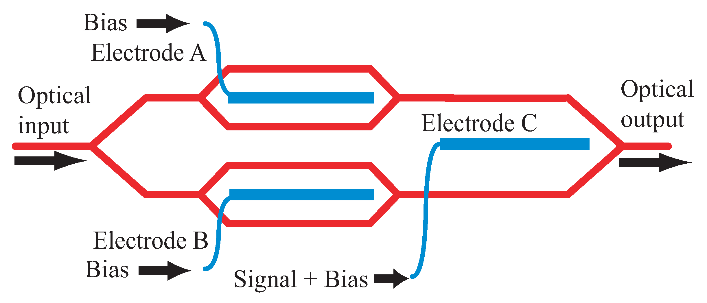
An integrated x-cut (LN) modulator with active trimmers can offer high ER intensity modulation [9]. As shown in Figure 2, the modulator has a pair of sub MZIs in a main MZI. The sub MZIs compensate imbalance in the main MZI due to fabrication error. The integrated LN modulator has three electrodes (A, B and C). The amplitude balance between the two arms in the main MZI, can be controlled by changing dc-bias voltages fed to the electrodes A and B. A modulation signal on the electrode C controls the optical phase difference between the two arms of the main MZI.
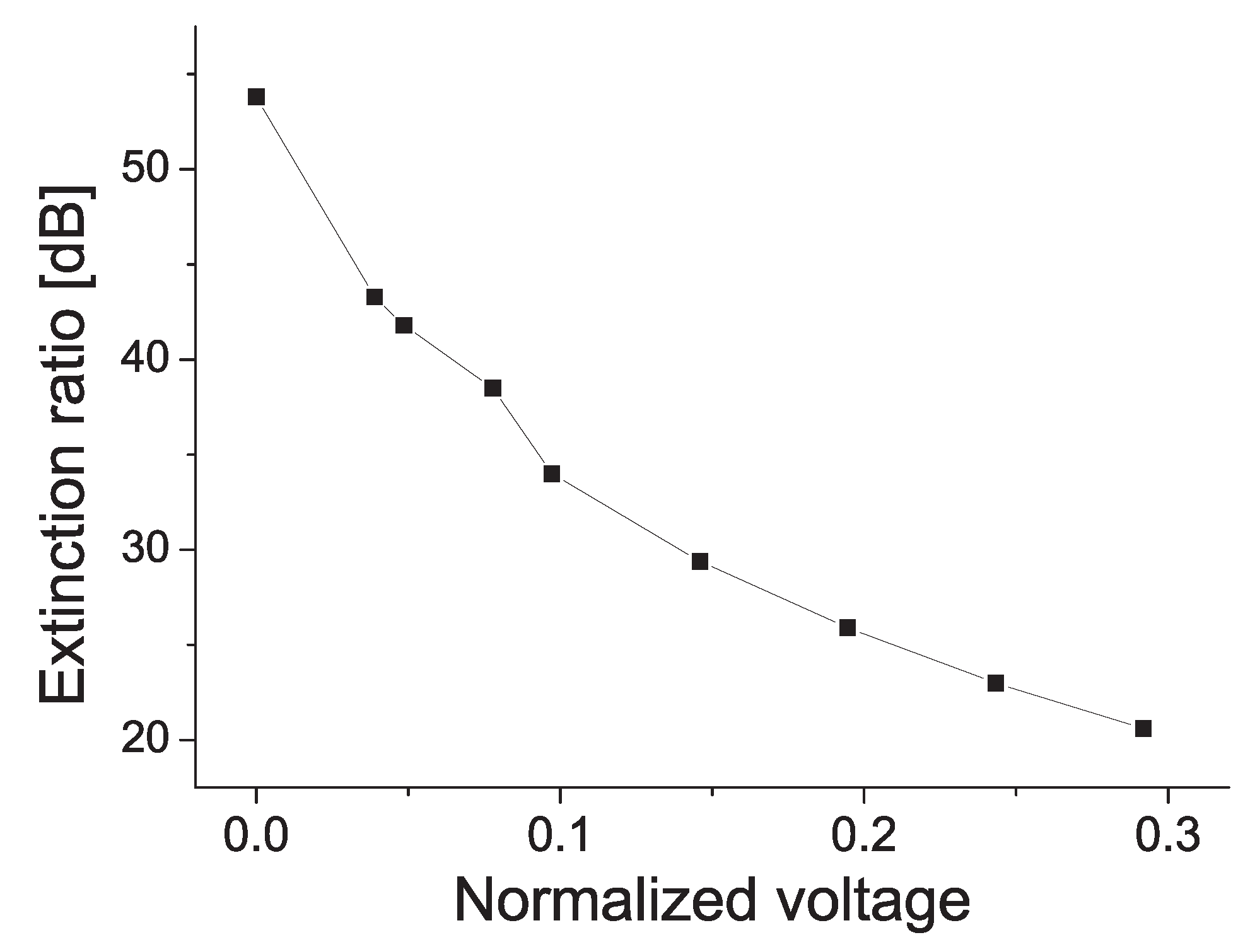
Figure 3 shows time-domain responses of the modulator, where the ERs with and without compensation were, respectively, 71 dB and 32 dB. Zero span operation of an optical spectrum analyzer was used to measure high extinction ratio on-off-keying. The rise and fall times of the time-domain profiles shown in Figure 3 were dominated by the response of the optical spectrum analyzer. Due to fabrication error, optical power in one arm of the MZM should be larger than that in the other arm. The optical power in the arm whose optical loss is larger than in the other arm should be adjusted by using a sub MZI [1]. As shown in Figure 4, the ER can be controlled by the voltage applied to the sub MZI embedded in the arm whose optical loss is larger than the other arm. The x-axis shows the dc-bias voltage offset from the imbalance compensated condition, where the scale was normalized by of the sub MZI. The ER-tuning range was from 21 dB to 54 dB.
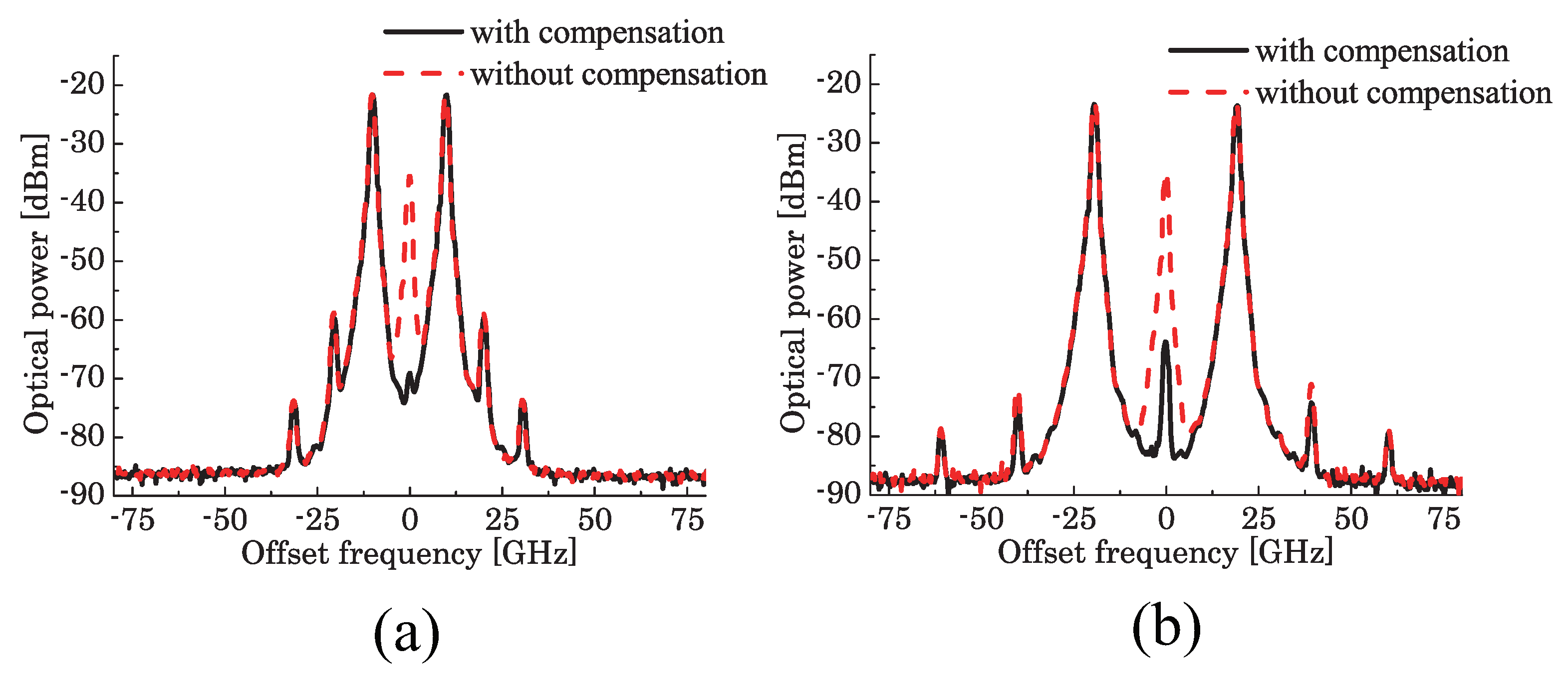
An MZM with minimum transmission bias can offer double sideband suppressed carrier (DSB-SC) modulation, where the carrier component is suppressed by destructive interference between optical waves propagating in the two waveguides of the main MZI. By feeding a sinusoidal single-tone signal as a modulating signal, we can generate an optical two-tone signal consisting of the first order USB and LSB with suppressed carrier. The suppression ratio depends on the imbalance between the optical waves, in other words, the ER of the modulator. Figure 5 shows optical spectra of optical two-tone signals generated by an MZM with active trimmers. The ER can be higher than 60 dB. The modulating signal frequencies were 10.5 GHz and 20.0 GHz. The main MZI wase set to be a minimum transmission bias condition. Carrier suppression ratios with respect to the first order USB or LSB were 47.4 dB for 10.5 GHz and 40.4 dB for 20.0 GHz, when the ER was enhanced by imbalance conpensation using the active trimmers. On the other hand the suppression ratios without compensation were less than 20 dB.
Parasitic optical phase modulation due to imbalance in induced phases on the two arms in the main MZI also causes generation of undesired high order sidebands. Such imbalance can be described by a chirp parameter [1]. The second order sideband generation was mainly due to the parasitic optical phase modulation associated with the chirp parameter , while the third order components are due to intrinsic nonlinearity of the MZMs. As described above, the chirp parameter can be largely suppressed by using a dual-electrode MZM [10].
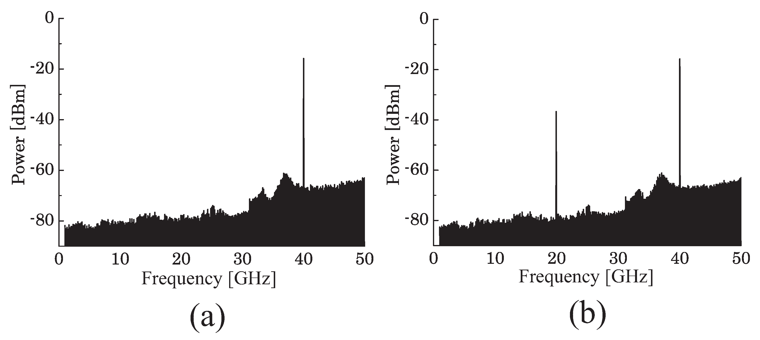
By using a high-speed photodetector, the optical two-tone signal can be converted into a pure single-tone electric signal as a beat signal of the two optical spectral components whose frequency separation is equal to . Figure 6a,b show wide span (DC-50 GHz) spectra of the RF signal generated from the optical two-tone signal (). with and without the compensation technique, respectively, where resolution bandwidth was 43 kHz. By using active trimming, the spurious suppression ratio could be larger than 60 dB without using any electrical or optical filters for suppression of undesired components, where the suppression ratio without using active trimming was 21.0 dB. The linewidth of the generated millimeter-wave signal was almost equal to that of the modulating signal.
4. Photodetector Response Measurement by Optical Two-Tone Signals
As shown in Figure 7, photodetector response can be measured by using an optical two-tone signal generated by an MZM with minimum transmission bias where the first order USB and LSB components are effectively obtained with large carrier suppression [16,17]. The optical power of the USB and LSB at the output port of the MZM depends on the modulation efficiency of the MZM, in other words, the frequency response of the MZM.
In general, amplitude modulated signals have USB and LSB in addition to the carrier component which corresponds to the input lightwave. The intensity of the USB or LSB with respect to the carrier reflects the modulation efficiency. The amplitude of the first order sideband is approximately proportional to that of the electric signal fed to the MZM as a modulating signal, while that of the carrier does not change largely under small signal approximation. On the other hand, the MZM with minimum transmission bias suppresses the carrier component, and generates equally power-balanced USB and LSB. The spectral shape does not depends on the response of the MZM, because the optical signal has only the two spectral components: the first order USB and LSB. The optical frequency separation between the USB and LSB is equal to double the frequency of the modulation signal fed to the MZM. Thus, the conversion efficiency of the photodetector can be calculated from the ratio between the optical power of the photodetector input and the RF power of the photodetector output , as follows:
where is the load impedance of the photodetector electric output. When is 50 , the response can be described by
where RF frequency is double that of the modulating signal, and the frequency sweep range can be also double that of the electric signal source for the MZM.
When the ER is not large enough, the optical power measurement would have error due to residual carrier component. High ER modulation is important to ensure precise measurement of photodetector conversion efficiency. By sweeping the frequency of the modulation signal fed to the MZM, we can measure the frequency response of the photodetector, as shown in Figure 8. When the supression ratio of undesired components including the optical carrier is large enough, the frequency response of the MZM does not affect the measurement results [16,17]. Thus, we can calibrate the frequency response of the photodetector, without measuring that of the modulator. The response of the modulator can be measured by a calibrated photodetector.
5. ER-Induced Phase Error in Optical Modulation
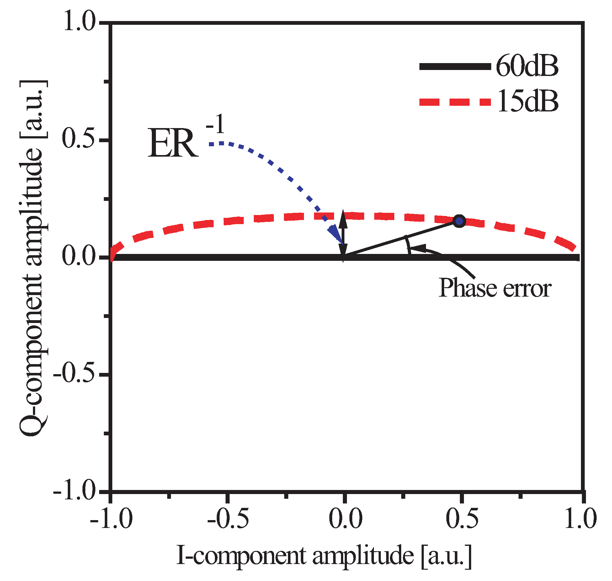
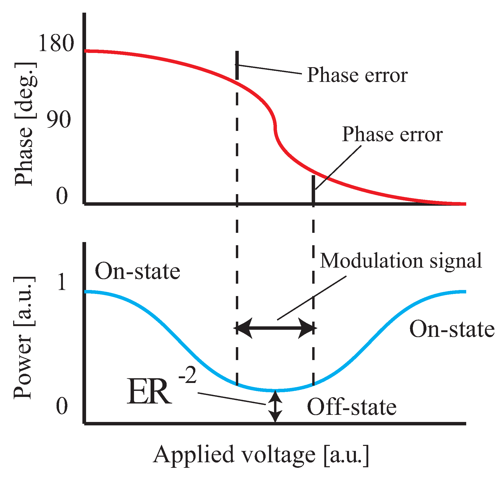
As described above, the intensities of optical signals propagating along the two arms of the MZM with push-pull operation should be balanced, in order to achieve pure amplitude modulation [1]. Due to the imbalance, the MZM outputs some residual optical power at an off-state where the phase difference between the two optical signals on the two arms is equal to 180 degrees. The off-state corresponds to the minimum transmission bias point, where the residual optical power depends on the imbalance. The ER can be defined by the ratio between optical power of an on-state and that of an off-state. As shown in Figure 9, the phase of the optical output would equal 0 or 180 degrees in an ideally balanced MZM which offers pure amplitude modulation. On the other hand, the response with a finite ER will rather be ellipsoidal on an IQ diagram, where the ratio between the major and minor axes is equal to the ER. Thus, the output optical has difference from 0 or 180 degrees, as shown in Figure 10. This phase error would be significant when the modulator is close to the off-state which corresponds to the origin of the complex plane.
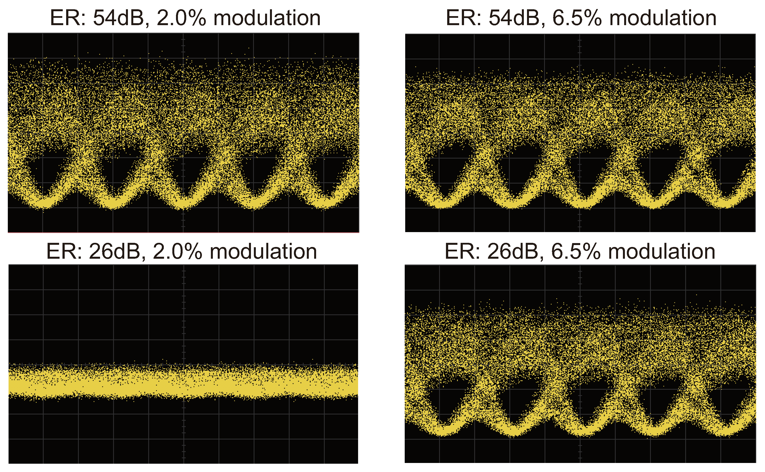
As shown in Figure 11, to investigate impact of the phase error due to finite ER, optical fiber transmission using duobinary modulation was demonstrated with varying ER [12]. A duobinary modulation signal was generated by using an integrated MZM with two small MZIs to control optical power balance in the main MZI, which a three-level signal fed to. The three-level signal was generated from a 10 Gb/s non-return-to-zero binary electric signal through a Bessel low pass filter. We can tune the ER of the MZM by changing the dc-bias voltages applied to the two sub-MZIs through electrodes A and B. The insertion loss at the integrated modulator was 4.7 dB. of the main and sub MZIs were 5 V at dc. The amplitude of the modulating signal was set to much smaller than the halfwave voltage of the MZM, to investigate the impact of the phase error for symbols close to the origin of the IQ diagram. The modulating signal amplitude fed to the main MZI through electrode C was 200 mV (peak-to-peak), which corresponds to of the full-swing operation () at dc ( modulation depth, henceforth).
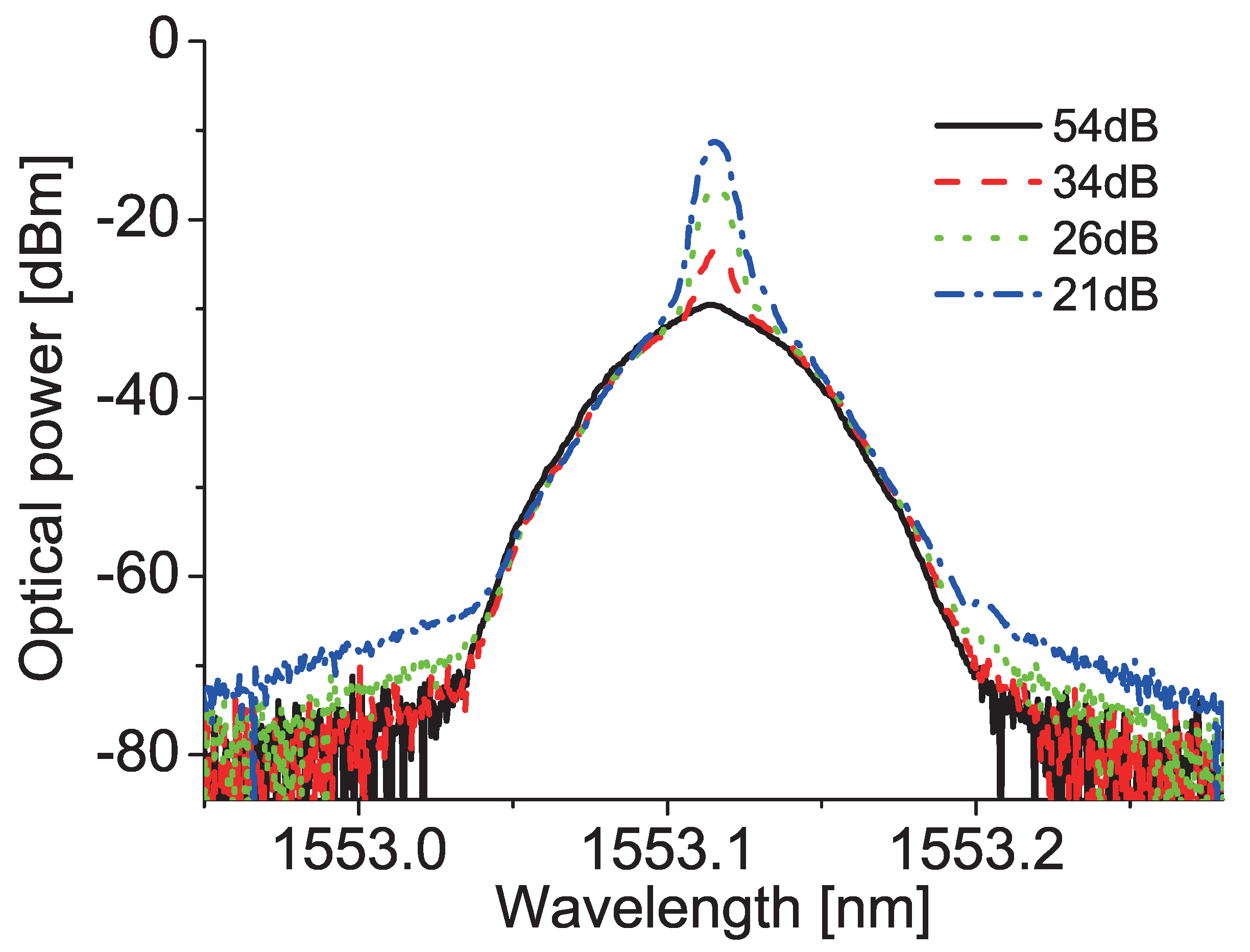
As shown in Figure 12, when ER was less than 35 dB, undesired residual carrier components were clearly observed in the optical spectra, where the optical power at the MZM input was 15 dBm. Due to finite ER, the carrier suppression was not large enough for small signal modulation. On the other hand, ideal duobinary modulation was achieved by the high ER modulation of , even if the modulation signal was very weak.
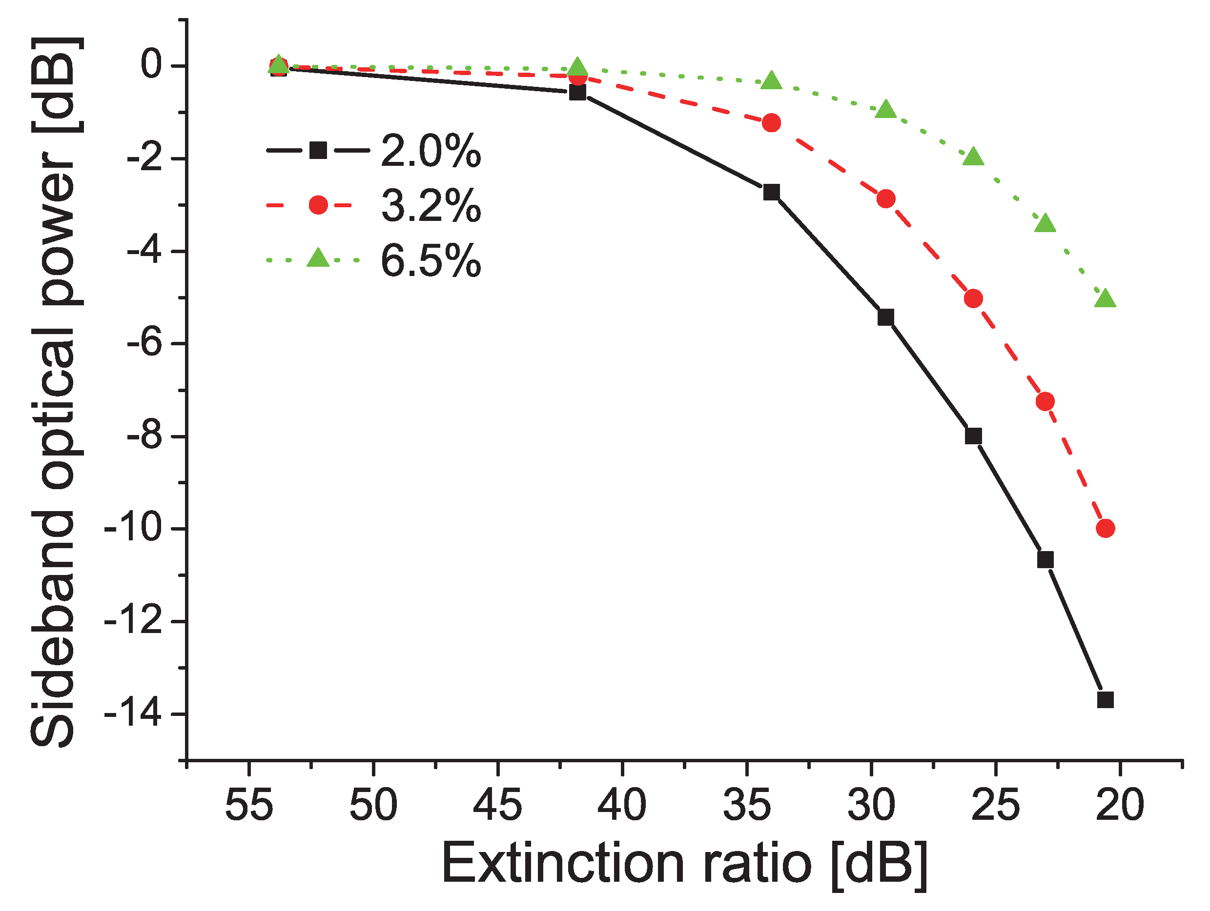
The sideband power which carries data information can be estimated from the measured optical spectra. Figure 13 shows the ratio between the sideband power and the total MZM output for various modulation depths: and . When the modulation depth is small, the ratio would be very sensitive to the ER. For example, when the modulation depth is , ER should be larger than to achieve the sideband ratio higher than , while is high enough with modulation depth. When the sideband ratio is small, the output lightwave would be dominated by the undesired carrier component.
Eye-diagrams of duobinary signals demodulated by envelop detection using a photodetector are shown in Figure 14, where modulation depths were and . Clear eye-opening was observed in both cases, when . On the other hand, when , the eye diagram for depth modulation was completely closed, while that for modulation depth was clearly open. Figure 15 shows required optical signal-to-noise-ratio (OSNR) with 0.1 nm bandwidth for BER of , for back-to-back (BTB) measurement. The required OSNR was sensitive to the ER when the modulation depth was small. High ER would offer clear eye-opening even when the modulation signal amplitude is very small. In other words, the effective sensitivity of the MZM can be enhanced by high-ER operation. Required OSNR can be largely reduced for a constant modulation depth.
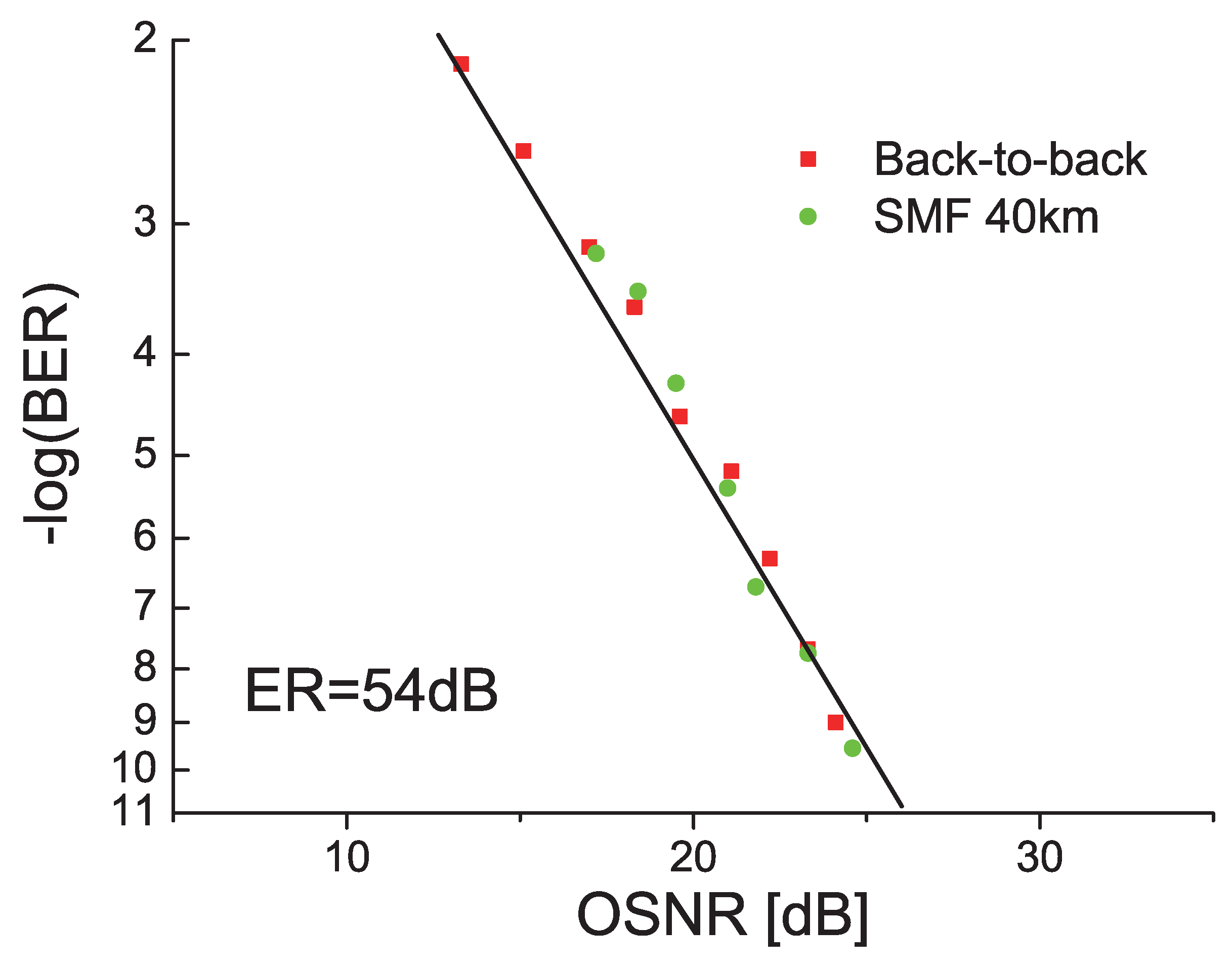
BER curves with , for BTB and transmission over 40 km SMF are shown in Figure 16, where OSNR required for BER was for BTB. The OSNR penalty due to 40 km transmission was less than 0.5 dB. As reported previously [18], OSNR required for BER was at 107 Gb/s. This result can be scaled by a factor of 10 for comparison with a 10-Gb/s system. The required OSNR translates to 24 dB, which agrees very well with the result.
6. Rapid Optical Frequency Sweep for Device Characterization
Optical SSB suppressed carrier modulation can be achieved by using a dual parallel MZM [1]. A pair of sinusoidal signals with 90-degree phase difference are fed to the two sub MZIs through electrodes and shown in Figure 17. The modulator is called an optical SSB modulator, where the optical phase difference between the two arms in the main MZI should be maintained to be 90-degree by dc-bias through electrode. The carrier component is suppressed at each sub MZI whose bias should be set to be a minimum transmission condition. One of sideband component (USB or LSB) is eliminated at the Y-junction of the main MZI. Thus, the output has only one spectral component whose frequency is or . is the optical frequency of the modulator input, while denotes the frequency of the modulating signal fed to the electrodes. The output optical frequency can be controlled by changing . Thus, an optical frequency sweeper can be configured by a dual parallel MZM and an RF signal sweeper [13,14,15].
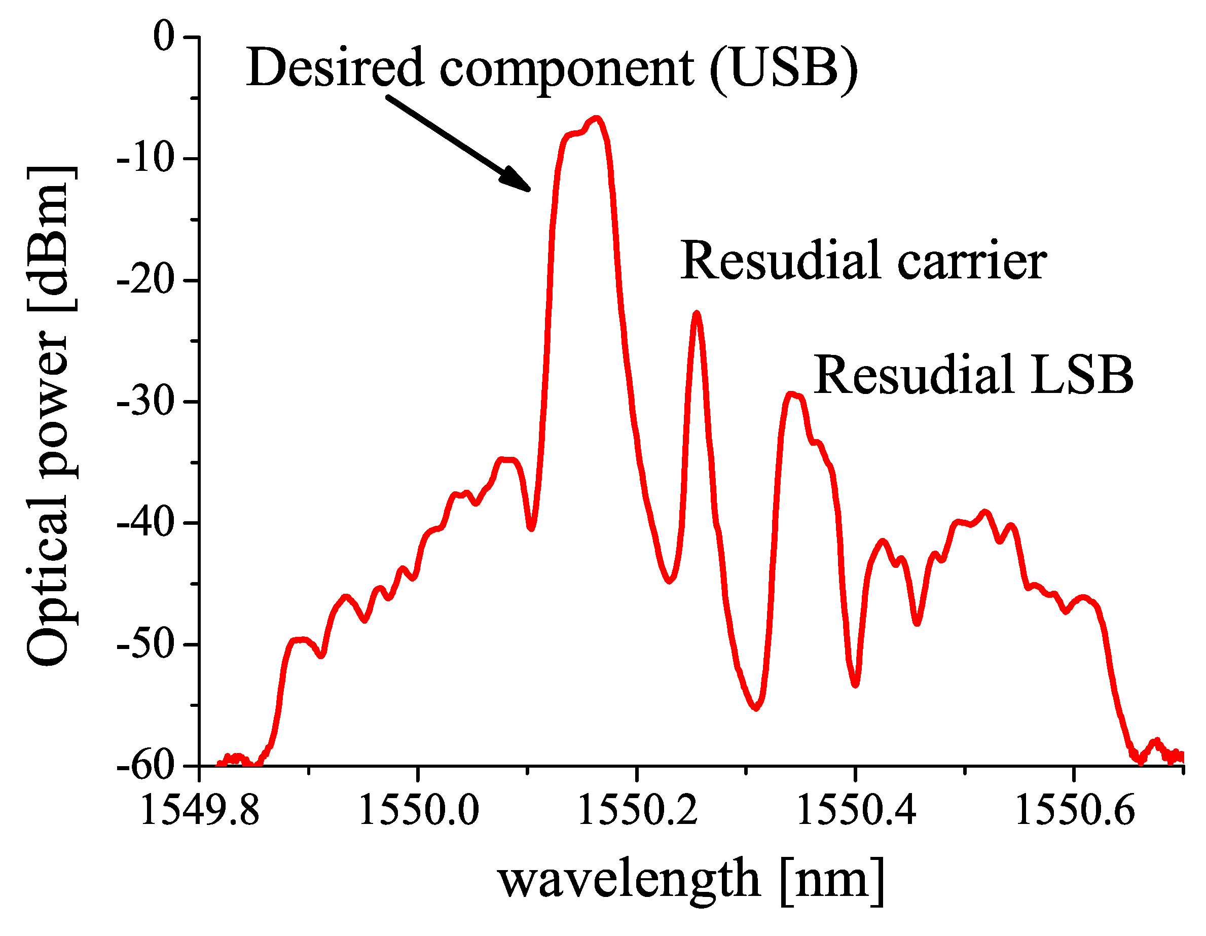
The optical frequency depends on the modulating signal frequency and dc-bias voltage fed to the modulator, which can be electronically controlled. Thus, output frequency can be swept agilely, where the frequency shift from optical input is precisely equal to . Figure 18 shows an optical-frequency sweeper setup. A wideband electric sweep signal, whose frequency range was from 9.6 GHz to 16.0 GHz, was generated by an arbitrary waveform generator (Tektronix AWG710B) and a wideband 32th-order frequency multiplier. The sweep frequency range at the arbitrary waveform generator was 300–500 MHz, where the sweep time was 500 ns, 250 ns, 200 ns or 100 ns. The wideband electric sweep signal was fed to an SSB modulator through a microwave amplifier and a hybrid coupler. The modulating signal power at each modulator input was 23 dBm. A tunable laser source was used for coarse wavelength control. The output optical signal from the modulator was fed to a device under test (DUT). Transmitted optical power through the DUT was measured by using a photodetector. The optical power without DUT was also measured for calibration. Optical transmittance of the DUT can be obtained from the ratio between the optical powers with and without DUT. The bias voltages were applied on the modulator was adjusted for USB generation. Figure 19 shows an optical spectrum at the output port of the modulator, where the sweep time of the optical frequency sweeper was 100 ns.
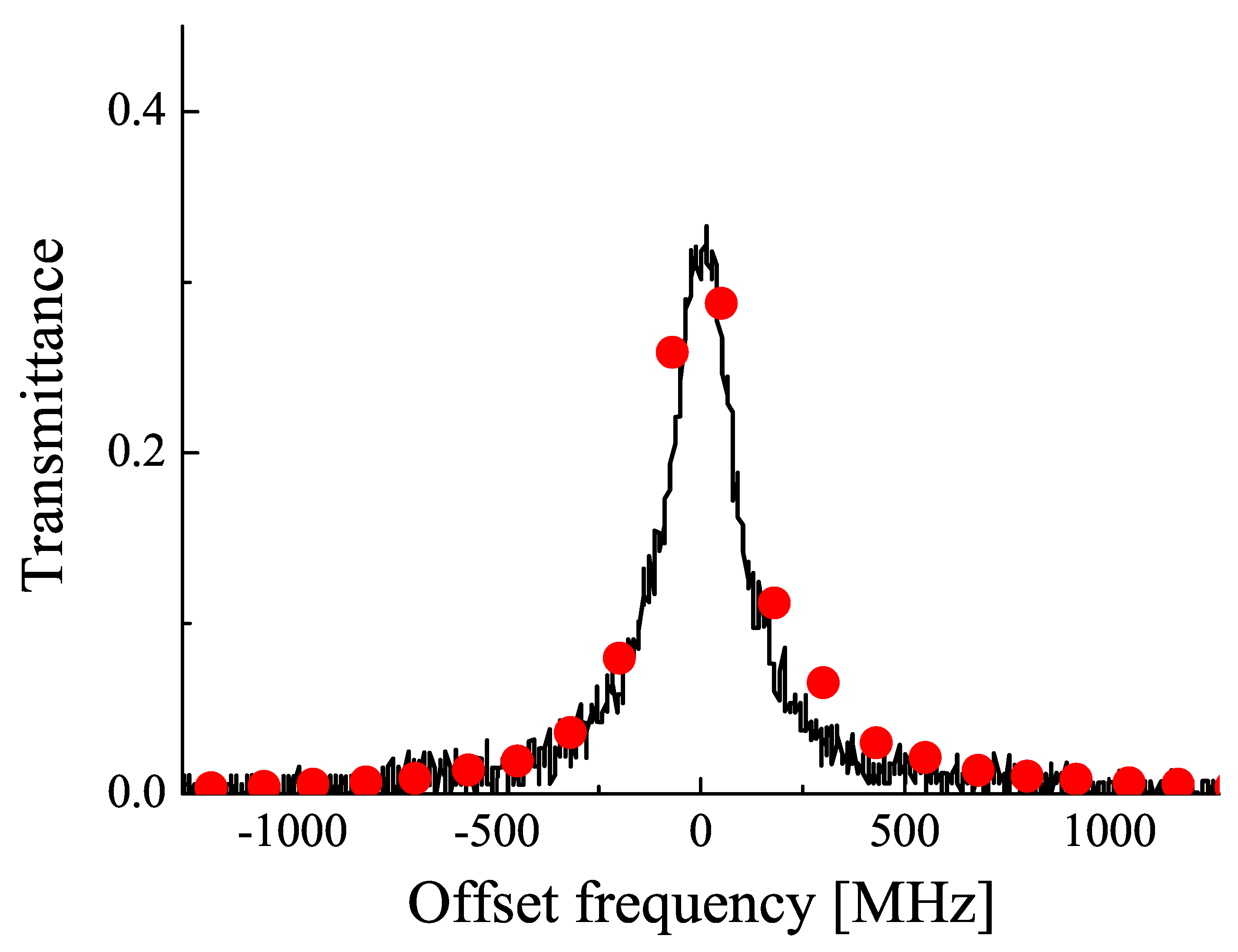
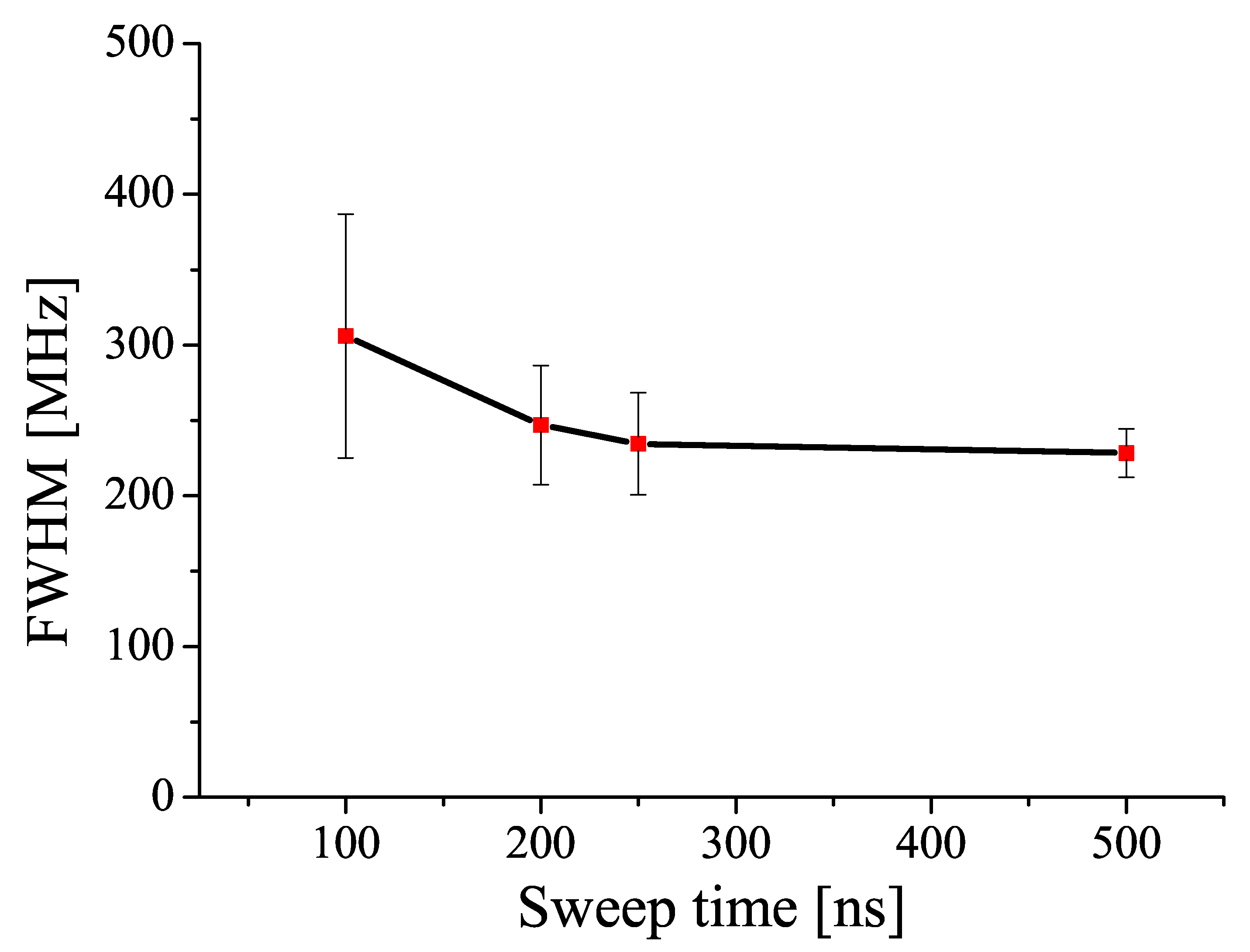
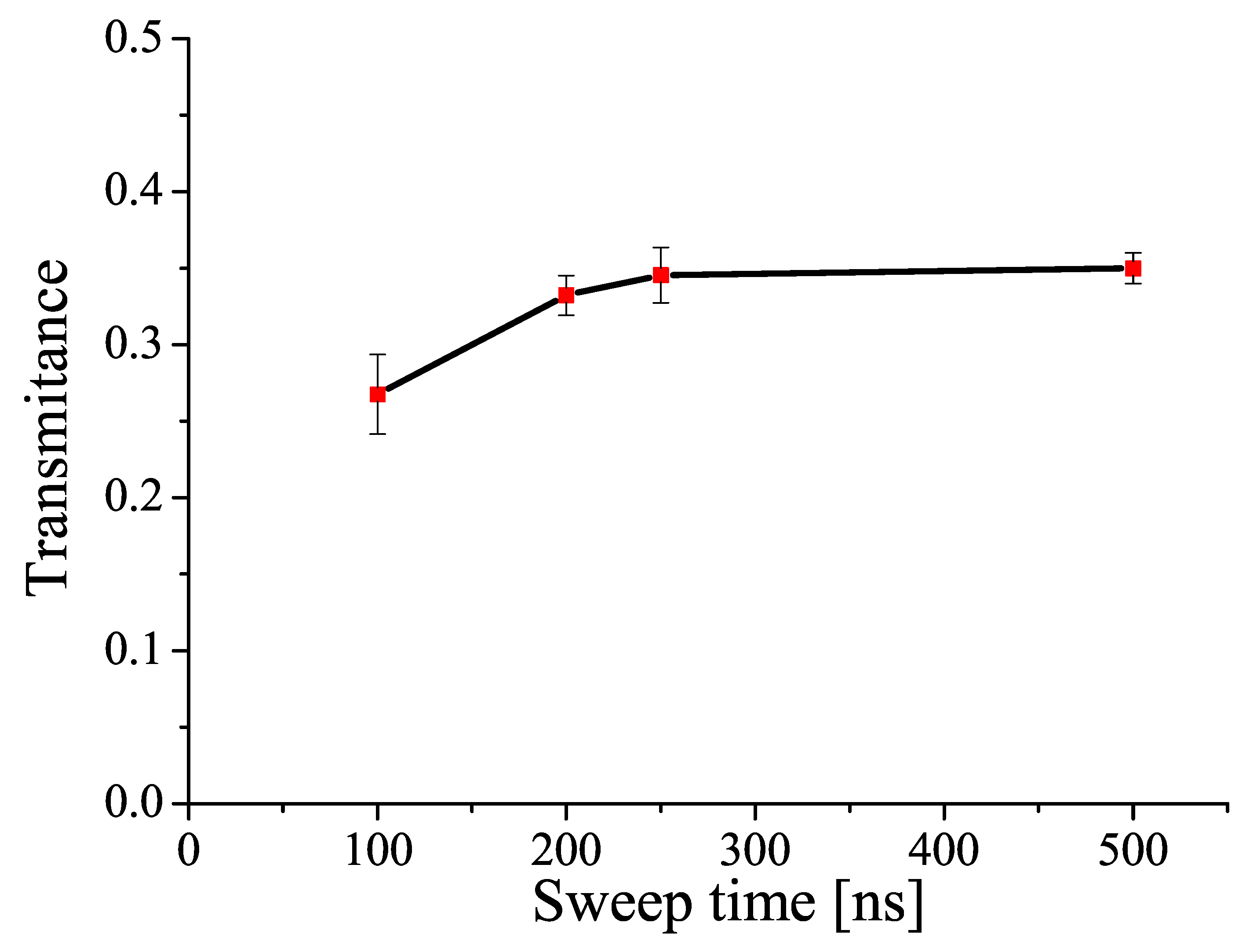
A narrow passband in the reflection band of a dual-section fiber Bragg grating (FBG) was measured by using the the fast optical frequency sweep system, where the sweep range and time were, respectively, 6.4 GHz and 0.5 s. The dual-section FBG had a few narrow passbands in the reflection band of the FBG. The frequency response can be obtained as a time domain profile. For comparison, we also measured the narrow passband by using a tunable laser (Agilent 81689A) where the sweep time was a few seconds. As shown in Figure 20, the two results agreed with each other very well, where the FWHM was 200 MHz. However in our proposing system, the sweep time was much faster than the conventional technique using a tunable laser. In order to estimate linearity of the frequency sweep in our system, we measured the time domain profiles of the FBG for various input lightwave frequencies, as shown in Figure 21, where the input lightwave frequency from the tunable laser was swept with 5 pm (625 MHz) step, which corresponds to 47 ns step in the time domain. The position deviation in x-axis between the adjacent traces should be close to the frequency sweep step at the tunable laser. By using this method, we investigated linearity and accuracy of the frequency sweep. Figure 22 shows the frequency deviations between the adjacent peaks, for various sweep time (500 ns, 250 ns, 200 ns and 100 ns). The frequency accuracy of the tunable laser was , so that the frequency deviations would be between the dashed lines in Figure 22 if the frequency error in the sweeper was smaller than that of the tunable laser. As shown in Figure 22, most of the points were between the dashed lines, so that we deduce that the frequency error in the sweep technique was negligibly small. Figure 23 shows the FWHM of the peaks as a function of the sweep time. When the sweep time is less than 200 ns, the FWHM became larger, due to the uncertainty between time and frequency. The frequency domain resolution is dominated by the linewidth of the laser source, however when the sweep time is short, the uncertanity between time and frequency would be the most important factor in the resolution. As shown in Figure 24, the sensitivity was small when the sweep time was short. Thus, the sweep time should be longer than 200 ns, in order to achieve precise measurement using our setup. However, we can obtain rough time-resolved frequency response measurement with 100 ns time domain resolution. The sweep time (repetition rate) can be easily changed by using the arbitrary waveform generator.
7. Conclusions
Optoelectronic devices which play important roles in high-speed optical fiber networks can offer effective measurement methods for optoelectronic devices including optical modulators and photodetectors. Precise optical signal modulation is required for measurement applications. This paper focused on high-speed and precise optical modulation devices and their application to device measurement. Optical modulators using electro-optic effect offers precise control of lightwaves for wideband signals. Extinction ratio and chirp parameter describe preciseness of optical modulation by Mach-Zehnder modulators. Precise and high-speed modulation can be achieved by active trimming which compensates device structure imbalance due to fabrication error. The extinction ratio can be larger than 50 dB, while that of a conventional modulator would be 20 dB. By using an optical modulator with high extinction ratio, we can generate optical two-tone signals which are useful for measurement applications. Spectral profiles of two-tone optical signals are independent from frequency response of the modulator. Thus, conversion efficiency of a photodetector can be easily calibrated by feeding an optical two-tone signal. Precise modulation would be also useful for advanced modulation techniques with many symbols. Constellations of multilevel modulation signals would be deformed by imperfection of modulators. To investigate impact of finite extinction ratio on optical modulation, duobinary modulation with small signal operation was demonstrated, where the three symbols would be close the null point which corresponds to the off-state of the modulator. Clear eye-opening was achieved by depth modulation, when the extinction ratio is larger than 50 dB. For optical frequency domain analysis, single sideband modulation, which sweeps optical frequency rapidly, generates stimulus optical signals. Fine spectral measurement of a 200 MHz narrow passband was demonstrated with 100 ns sweep time, where the sweep repetition rate was 10 MHz.
Funding
This research received no external funding.
Institutional Review Board Statement
Not applicable.
Informed Consent Statement
Not applicable.
Acknowledgments
This work was partially supported by Waseda Research Institute for Science and Engineering.
Conflicts of Interest
The authors declare no conflict of interest.
References
- Kawanishi, T.; Sakamoto, T.; Izutsu, M. High-Speed Control of Lightwave Amplitude, Phase, and Frequency by Use of Electrooptic Effect. IEEE J. Sel. Top. Quantum Electron. 2007, 13, 79–91. [Google Scholar] [CrossRef]
- Yamaguchi, Y.; Kanno, A.; Kawanishi, T.; Izutsu, M.; Nakajima, H. Precise Optical Modulation Using Extinction-Ratio and Chirp Tunable Single-Drive Mach?Zehnder Modulator. J. Light. Technol. 2017, 35, 4781–4788. [Google Scholar] [CrossRef]
- Zhang, F.; Zhang, L.; Ruan, X.; Yang, F.; Ming, H.; Li, Y. High Baud Rate Transmission With Silicon Photonic Modulators. IEEE J. Sel. Top. Quantum Electron. 2021, 27, 1–9. [Google Scholar] [CrossRef]
- Lu, G.-W.; Zhang, H.-B.; Shinada, S.; Hong, J.; Cheng, Y.; Yokoyama, S. Power-Efficient O-Band 40 Gbit/s PAM4 Transmitter Based on Dual-Drive Cascaded Carrier-Depletion and Carrier-Injection Silicon Mach-Zehnder Modulator With Binary Driving Electronics at CMOS Voltages. IEEE J. Sel. Top. Quantum Electron. 2021, 27, 1–8. [Google Scholar] [CrossRef]
- Ogiso, Y.; Ozaki, J.; Ueda, Y.; Wakita, H.; Nagatani, M.; Yamazaki, H.; Nakamura, M.; Kobayashi, T.; Kanazawa, S.; Hashizume, Y.; et al. 80-GHz Bandwidth and 1.5-V Vπ InP-Based IQ Modulator. J. Light. Technol. 2020, 38, 249–255. [Google Scholar] [CrossRef]
- Irmscher, S.; Lewen, R.; Eriksson, U. InP-InGaAsP high-speed traveling-wave electroabsorption modulators with integrated termination resistors. IEEE Photonics Technol. Lett. 2002, 14, 923–925. [Google Scholar] [CrossRef]
- Kawanishi, T.; Kanno, A.; Freire, H.S.C. Wired and Wireless Links to Bridge Networks: Seamlessly Connecting Radio and Optical Technologies for 5G Networks. IEEE Microw. Mag. 2018, 19, 102–111. [Google Scholar] [CrossRef]
- Kawanishi, T. Wired and Wireless Seamless Access Systems for Public Infrastructure; Artech House: Norwood, MA, USA, 2020. [Google Scholar]
- Kawanishi, T.; Sakamoto, T.; Tsuchiya, M.; Izutsu, M. High extinction ratio optical modulator using active intensity trimmers. In Proceedings of the 2005 31st European Conference on Optical Communication, ECOC 2005, Glasgow, UK, 25–29 September 2005; Volume 4, pp. 841–842. [Google Scholar] [CrossRef]
- Kawanishi, T.; Sakamoto, T.; Chiba, A.; Tsuchiya, M.; Toda, H. Ultra high extinction-ratio and ultra low chirp optical intensity modulation for pure two-tone lightwave signal generation. In Proceedings of the 2008 Conference on Lasers and Electro-Optics and 2008 Conference on Quantum Electronics and Laser Science, San Jose, CA, USA, 4–9 May 2008; pp. 1–2. [Google Scholar]
- Kawanishi, T.; Sakamoto, T.; Chiba, A.; Izutsu, M. Study of precise optical modulation using Mach-Zehnder interferometers for advanced modulation formats. In Proceedings of the 33rd European Conference and Exhibition of Optical Communication, Berlin, Germany, 16–20 September 2007; pp. 1–2. [Google Scholar] [CrossRef]
- Kawanishi, T.; Sakamoto, T.; Chiba, A.; Izutsu, M.; Winzer, P.J. Duobinary signal generation using high-extinction ratio modulation. In Proceedings of the OFC/NFOEC 2008-2008 Conference on Optical Fiber Communication/National Fiber Optic Engineers Conference, San Diego, CA, USA, 24–28 February 2008; pp. 1–3. [Google Scholar] [CrossRef]
- Kawanishi, T.; Sakamoto, T.; Izutsu, M. Optical frequency sweep technique using single sideband modulation. In Proceedings of the 2005 31st European Conference on Optical Communication, ECOC 2005, Glasgow, UK, 25–29 September 2005; Volume 3, pp. 635–636. [Google Scholar] [CrossRef]
- Kawanishi, T.; Sakamoto, T.; Fonseca, D.; Cartaxo, A.; Monteiro, P.; Izutsu, M. Fine Transmittance/Reflectivity Measurement System Using Single-Sideband Frequency Sweeper with Ultra-Wideband Hilbert Transformer. In Proceedings of the 2006 European Conference on Optical Communications, Cannes, France, 24–28 September 2006; pp. 1–2. [Google Scholar] [CrossRef]
- Kawanishi, T.; Sakamoto, T.; Izutsu, M. Fast optical frequency sweep for ultra-fine real-time spectral domain measurement. Electron. Lett. 2006, 42, 999–1000. [Google Scholar] [CrossRef]
- Inagaki, K.; Kawanishi, T.; Izutsu, M. Optoelectronic frequency response measurement of photodiodes by using high-extinction ratio optical modulator. IEICE Electron. Express 2012, 9, 220–226. [Google Scholar] [CrossRef] [Green Version]
- Inagaki, K.; Kawanishi, T.; Iwai, H.; Oikawa, Y. Development of lightwave frequency response analyzer for characterizing O/E conversion devices. In Proceedings of the 2014 International Topical Meeting on Microwave Photonics (MWP) and the 2014 9th Asia-Pacific Microwave Photonics Conference (APMP), Hokkaido, Japan, 20–23 October 2014; pp. 113–116. [Google Scholar] [CrossRef]
- Winzer, P.J.; Raybon, G.; Doerr, C.R.; Duelk, M.; Dorrer, C. 107-Gb/s optical signal generation using electronic time-division multiplexing. J. Light. Technol. 2006, 24, 3107–3113. [Google Scholar] [CrossRef]
Figure 1.
MZM structure.

Figure 2.
Integrated MZM with two active trimmers.

Figure 3.
On-off-keying by an MZM with and without imbalance compensation [1].
Figure 3.
On-off-keying by an MZM with and without imbalance compensation [1].

Figure 4.
Extinction ratio controlled by a sub-MZI [12].
Figure 4.
Extinction ratio controlled by a sub-MZI [12].

Figure 5.
Spectra of optical two-tone signals with = 10.5 GHz (a) and 20 GHz (b) [1].
Figure 5.
Spectra of optical two-tone signals with = 10.5 GHz (a) and 20 GHz (b) [1].

Figure 6.
Spectra of RF signals generated from optical two-tone signals with compensation (a) and without compensation (b) [1].
Figure 6.
Spectra of RF signals generated from optical two-tone signals with compensation (a) and without compensation (b) [1].

Figure 7.
Photodetector measurement by an optical two-tone signal.

Figure 8.
Measured photodetector frequency response.

Figure 9.
IQ diagrams of optical outputs from MZMs, where ERs were 15 dB and 60 dB [12].
Figure 9.
IQ diagrams of optical outputs from MZMs, where ERs were 15 dB and 60 dB [12].

Figure 10.
Schematic of optical phase and amplitude response of an MZM with finite ER [12].
Figure 10.
Schematic of optical phase and amplitude response of an MZM with finite ER [12].

Figure 11.
Experimental setup for duobinary transmission [12].
Figure 11.
Experimental setup for duobinary transmission [12].

Figure 12.
Optical spectra of duobinary signals with various ERs [12].
Figure 12.
Optical spectra of duobinary signals with various ERs [12].

Figure 13.
Sideband ratio to total optical output [12].
Figure 13.
Sideband ratio to total optical output [12].

Figure 14.
Eye-diagrams for modulation depths of and [12].
Figure 14.
Eye-diagrams for modulation depths of and [12].

Figure 15.
Required OSNR for BER , where the modulation depths were , and [12].
Figure 15.
Required OSNR for BER , where the modulation depths were , and [12].

Figure 16.
Bit error ratio for back-to-back and 40 km SMF [12].
Figure 16.
Bit error ratio for back-to-back and 40 km SMF [12].

Figure 17.
Optical SSB modulator.

Figure 18.
Setup for optical frequency sweeper.

Figure 19.
Output optical spectrum.

Figure 20.
Transmittance of a narrow passband in a dual section FBG, where x-axis shows offset frequency from the center of the passband, Solid line and dots denotes results by the fast sweeper using an SSB modulator and conventional technique using a tunable laser, respectively.
Figure 20.
Transmittance of a narrow passband in a dual section FBG, where x-axis shows offset frequency from the center of the passband, Solid line and dots denotes results by the fast sweeper using an SSB modulator and conventional technique using a tunable laser, respectively.

Figure 21.
Transmittance of a narrow passband for various input lightwave wavelength, in time-domain.
Figure 21.
Transmittance of a narrow passband for various input lightwave wavelength, in time-domain.

Figure 22.
Peak position deviations with source laser sweep in 625 MHz step, where the frequency accuracy of the laser was 125 MHz.
Figure 22.
Peak position deviations with source laser sweep in 625 MHz step, where the frequency accuracy of the laser was 125 MHz.

Figure 23.
FWHMs of the passband for various sweep times.

Figure 24.
Transmittance of the passband for various sweep times.

Publisher’s Note: MDPI stays neutral with regard to jurisdictional claims in published maps and institutional affiliations. |
© 2021 by the author. Licensee MDPI, Basel, Switzerland. This article is an open access article distributed under the terms and conditions of the Creative Commons Attribution (CC BY) license (https://creativecommons.org/licenses/by/4.0/).
Share and Cite
MDPI and ACS Style
Kawanishi, T. Precise Optical Modulation and Its Application to Optoelectronic Device Measurement. Photonics 2021, 8, 160. https://0-doi-org.brum.beds.ac.uk/10.3390/photonics8050160
AMA Style
Kawanishi T. Precise Optical Modulation and Its Application to Optoelectronic Device Measurement. Photonics. 2021; 8(5):160. https://0-doi-org.brum.beds.ac.uk/10.3390/photonics8050160
Chicago/Turabian StyleKawanishi, Tetsuya. 2021. "Precise Optical Modulation and Its Application to Optoelectronic Device Measurement" Photonics 8, no. 5: 160. https://0-doi-org.brum.beds.ac.uk/10.3390/photonics8050160
Note that from the first issue of 2016, this journal uses article numbers instead of page numbers. See further details here.