Structural Damage of Two-Dimensional Organic–Inorganic Halide Perovskites


1
School of Physical Science and Technology, ShanghaiTech University, Shanghai 201210, China
2
Davidson School of Chemical Engineering, Purdue University, West Lafayette, IN 47907, USA
*
Author to whom correspondence should be addressed.
Inorganics 2020, 8(2), 13; https://0-doi-org.brum.beds.ac.uk/10.3390/inorganics8020013
Submission received: 31 December 2019
/
Revised: 21 January 2020
/
Accepted: 25 January 2020
/
Published: 6 February 2020
(This article belongs to the Special Issue Inorganic Materials for Solar Energy Conversion)
Abstract
:Organic–inorganic halide perovskites are promising photovoltaic materials with excellent optoelectronic properties. However, the extreme structural instability hinders their wide application as well as the microstructure characterization using high energy beams such as transmission electron microscopy (TEM). Here, taking BA2FAPb2I7 and BA2MAPb2I7 as examples, we investigate their structural evolution resulting from high energy electron irradiation, moist air, and low temperature, respectively. The results show that the long organic chains are the first to be damaged under electron beam, which is mainly arising from their instability and weak bonding with the framework of [PbI6]4− octahedrons. Then the short organic cations and the framework of [PbI6]4− octahedrons collapses gradually. The final products are clusters of detached PbI2 particles, which can also be observed in the sample degraded in moist air. In addition, the structures of BA2FAPb2I7 and BA2MAPb2I7 are discovered to undergo a phase transformation at liquid nitrogen temperature, which calls attention to the community that cryo-TEM methods should be used cautiously for organic–inorganic halide perovskite materials.

1. Introduction
Two-dimensional (2D) organic–inorganic halide perovskites have attracted significant research interests owing to their wide tunability and excellent optical/electronic properties [1,2]. The efficiency of 2D perovskite solar cells has been increasingly improved and perovskite solar cells show tremendous advantages over silicon solar cells [3,4,5]. The perovskite bulk structure has the general formula of ABX3, where the A-site cations are normally inorganic alkali ions Cs+, Rb+, or can be substituted by short organic cations CH3NH3+ (methylammonium, MA) or CH(NH2)2+ (formamidinium, FA). The BX3 are octahedrons composed of Pb2+ (or Sn2+) and halide ions. In contrast to the bulk perovskites, 2D halide perovskites are usually formed in organic–inorganic hybrid phases, with separated octahedral [BX6]4− layers jointed by long organic chains, such as n-butylammonium (n-BA+), bithiophene (2T), and tetrathiophene (4T). It is expected that all-inorganic 2D layered structure is difficult to obtain as it is not so easy to separate the layers without chains in between. A case of all-inorganic 2D CsPbBr3 has just been reported recently [6,7]. It is well recognized that the performance of the 2D halide perovskites solar cells is closely related to the structure, especially their microstructure. Transmission electron microscopy (TEM) has been widely used to study the crystal structure and real atomic resolution is achieved in the recent decades owing to aberration correction [8]. However, halide perovskites are found to be electron-beam sensitive that hinders high resolution imaging [2]. With carefully controlling of the electron dose, atomic resolution has been demonstrated on the inorganic 2D halide perovskites [6]. However, hybrid 2D perovskites are still difficlut to be characterized as the organic portions are even more beam-sensitive. Apart from electron beam irradiation during characterization, humidity is another important factor to be considered, which results in detrimental effect on the photovoltaic efficiency and stability, hampering the wide application in solar cells [9]. Up to now, the mechanism of the structure sensitivity to electron irradiation and water molecules has not been clearly illustrated yet. In addition, the resultant damaged products are still controversial [6,10,11,12].
Taking 2D BA2FAPb2I7 and BA2MAPb2I7 as examples, this report investigates the structural changes arising from high-energy electron irradiation, moist air, as well as temperature change, respectively. The conclusion is made based on the analysis of selected-area electron diffraction (SAED) and high-resolution transmission electron microscopy (HRTEM) under low dose-rate electron beam irradiation. The structural destruction and resultant products under electron irradiation are analyzed in detail and the effect of moist air has also been studied as well. The process of structural destruction is highly related with the bonding strength of different structural units. Furthermore, structural evolution at low temperature is also evaluated.
2. Results
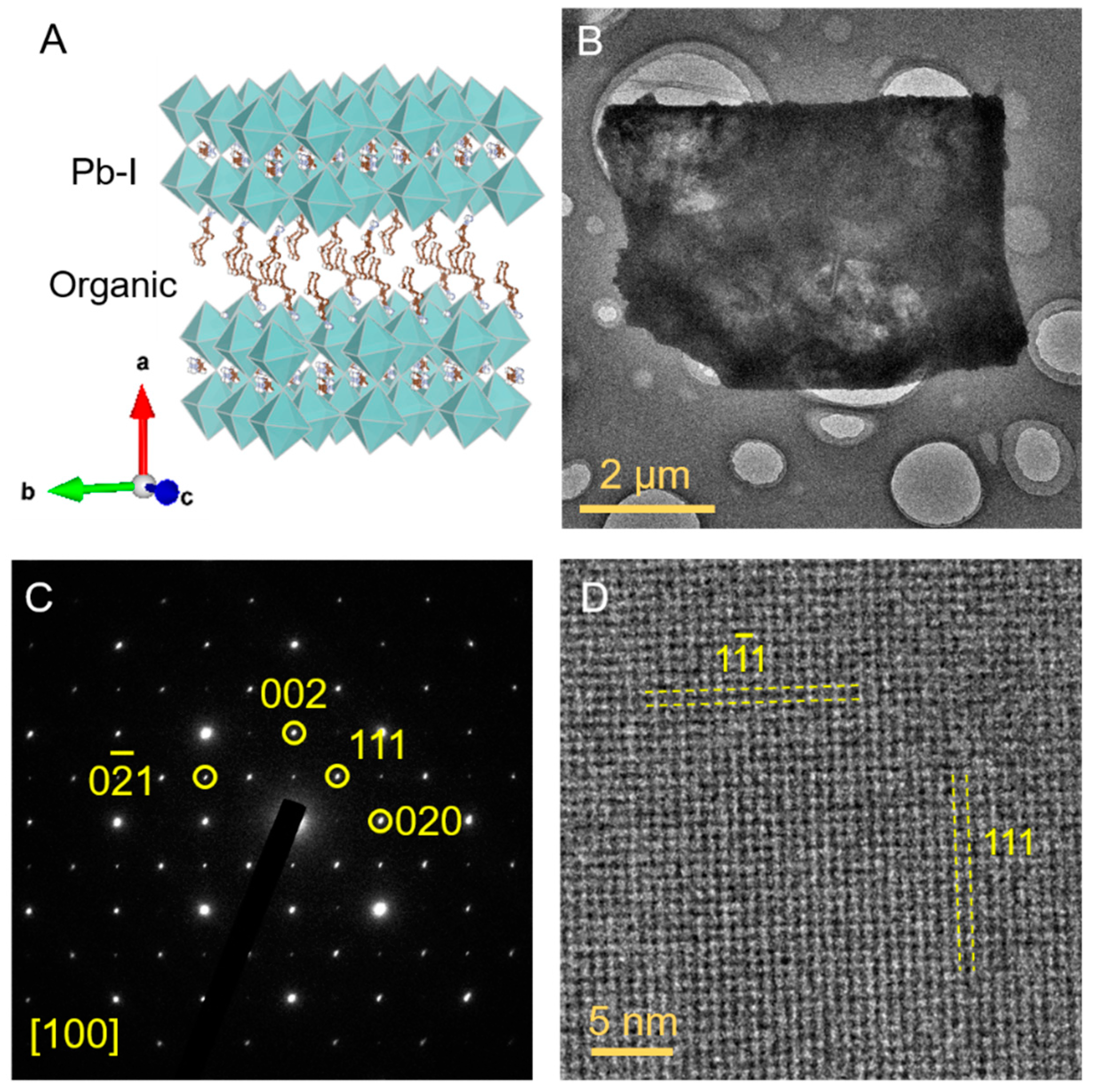
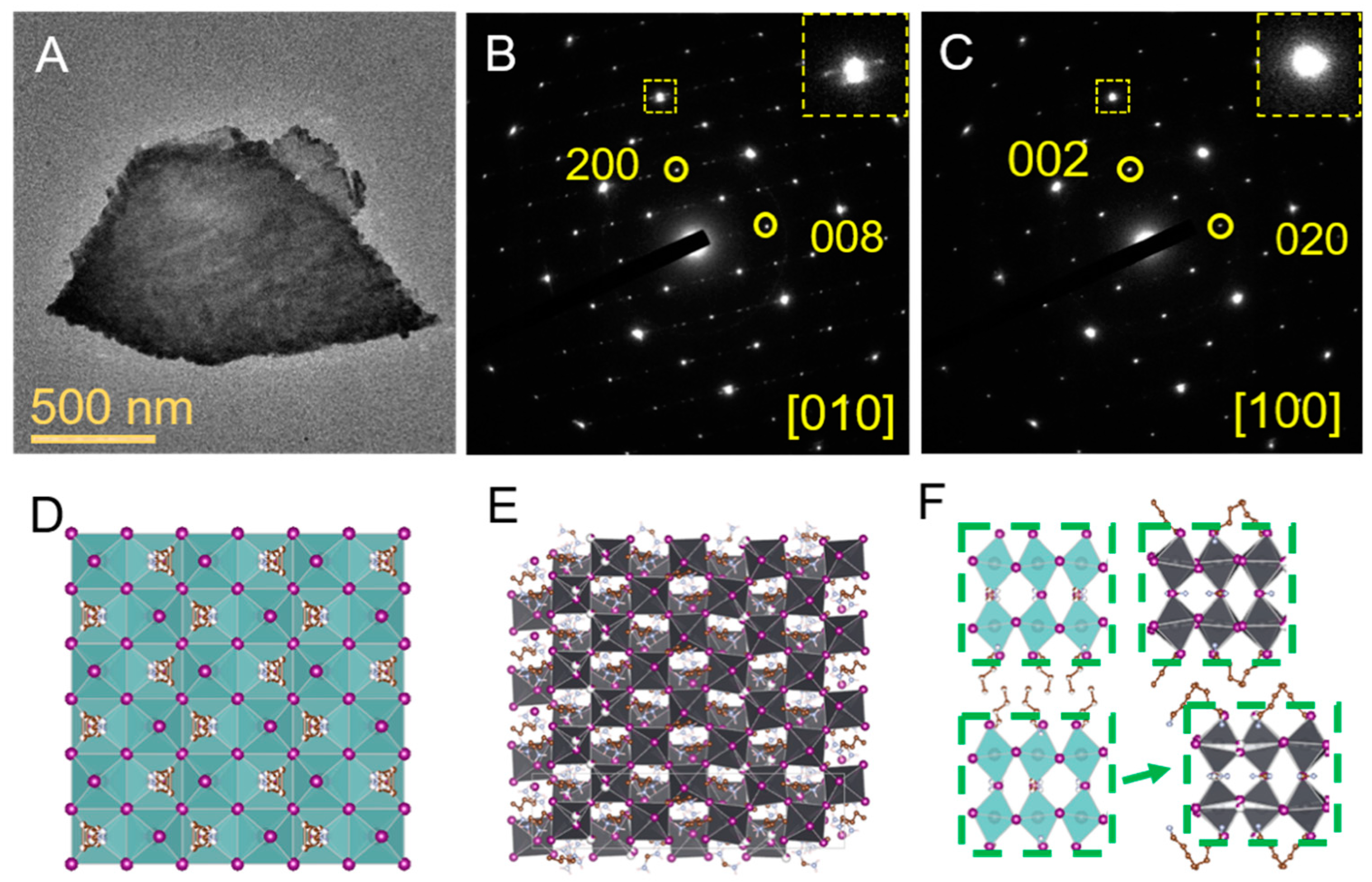
As an example, the layered crystal structure of BA2MAPb2I7 is shown in Figure 1A. Different from the bulk ABX3 formula, layered 2D structure has the general formula of An+1BnX3n+1, consisting of alternated ABX3 and AX layers, which is also known as Ruddlesden-Popper (RP) phase [7]. Here, the index n = 2 and the A-site is occupied by BA+ or MA+ organic groups. The B-site lead (Pb) atoms are embedded in octahedral voids surrounded by iodide (I) atoms. The framework structure of lead-iodide (Pb–I) layer is formed by Pb–I octahedrons connecting with corner-shared I atoms. The Pb-I layer is separated by weakly bonded organic long chain, which is the main reason that the 2D perovskites can be mechanically exfoliated. The crystal structure shown here was solved by single crystal X-ray diffraction at 310 K (detailed in Table S1). By substituting MA+ with FA+, the BA2FAPb2I7 may share the same structure as BA2MAPb2I7 at room temperature, and SAED index for BA2FAPb2I7 and BA2MAPb2I7 is based on the above crystal structure. The morphology of a 2D BA2FAPb2I7 sheet with ~5 by 5 µm in length is shown in Figure 1B. The corresponding SAED pattern in Figure 1C depicts the perfect crystallinity. It should be noted that several diffraction spots that do not belong to the zero order Laue zone appear in the pattern owing to the large excitation error of such thin sheet. The HRTEM image along [100] the zone axis was acquired at the dose-rate of less than 50 e− Å−2 s−1. In order to enhance the signal for noisy low dose data, average background subtraction filtering (ABSF) was applied to the raw image and the ABSF-filtered image is shown in Figure 1D [13]. Hence, clear orthogonal lattice fringes can be observed.
In the following, the effect of electron irradiation was evaluated by monitoring the structural change in sequential HRTEM images. Figure 2A–C shows three sequential ABSF-filtered HRTEM images acquired at the dose-rate of ~180 e− Å−2 s−1. The exposure time of each image is 200 ms and the raw images are shown in Figure S1. The Fourier transform (FT) of HRTEM image reveals the frequency information in reciprocal space, where a spot in reciprocal space corresponds to a set of lattice planes in real space. The evolution of Fourier spots is easier to be distinguished compared to images and therefore it could be used as a criterion to evaluate the structural damage.
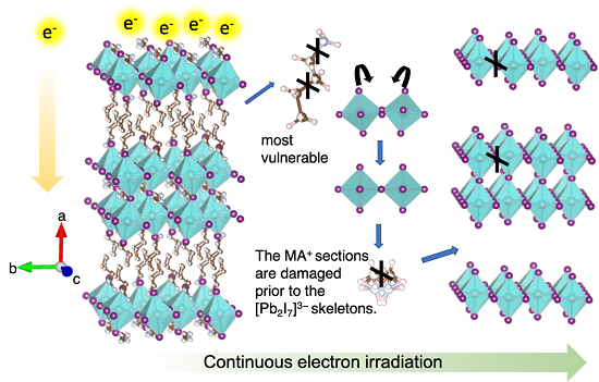
Compared to the diffraction pattern of almost intact sample (Figure 1C), the initial disappeared spots correspond to (01) and (0) plane (Figure 2E). At this moment, the lattice in real-space image is relatively uniform (Figure 2A). As the total dose accumulating further, the FT spots corresponding to (), (11), and (00) planes fade away gradually (Figure 2F). At the same time, the edge of originally uniform lattices begins to fade away in Figure 2B. After further electron irradiation, the nearest (1) and (11) spots in Figure 2G continue to disappear, and the corresponding HRTEM image demonstrates that the uniform nanosheet is destructed to a smaller region, where the edge of the crystalline region is indicated by dotted line in Figure 2C. By comparing with the crystal structure of Rm PbI2 [14], the FT pattern is consistent with the simulated SAED pattern along the zone axis [48] and HRTEM image is also consistent with structure of PbI2 in [48] projection (Figure 2D,H). Comparing the FT pattern of Figure 2F with Figure 2G, the nearest four {11} spots (6 Å) disappear and only the outer spots (3 Å) remain. The 6 Å and 3 Å lattices represent the distances of Pb–I–Pb in octahedron and Pb–I respectively. Hence, it can be inferred that finally the skeleton of Pb–I octahedron gradually collapses into small domains composed of PbI2 when exposed to high-energy electron beam.
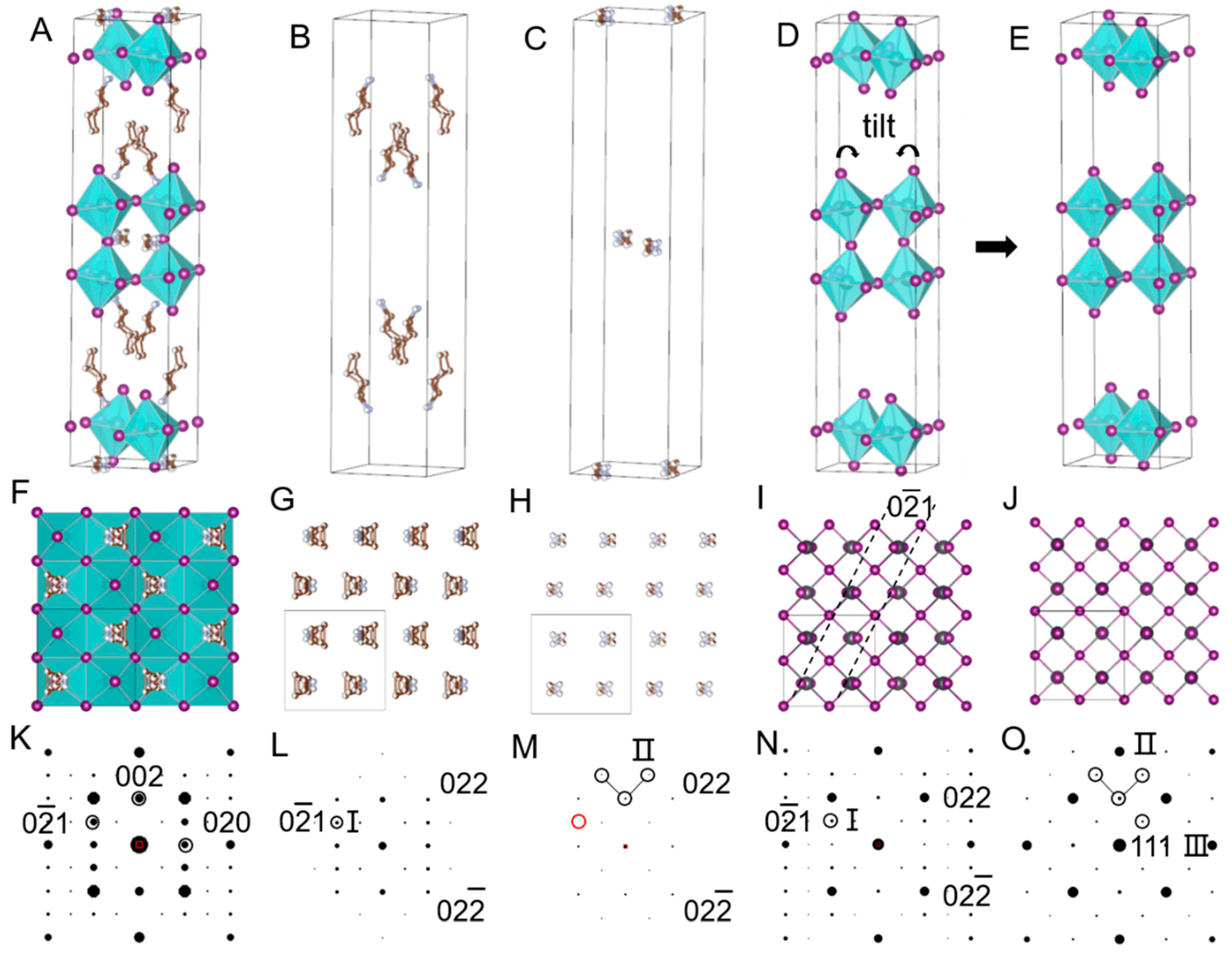
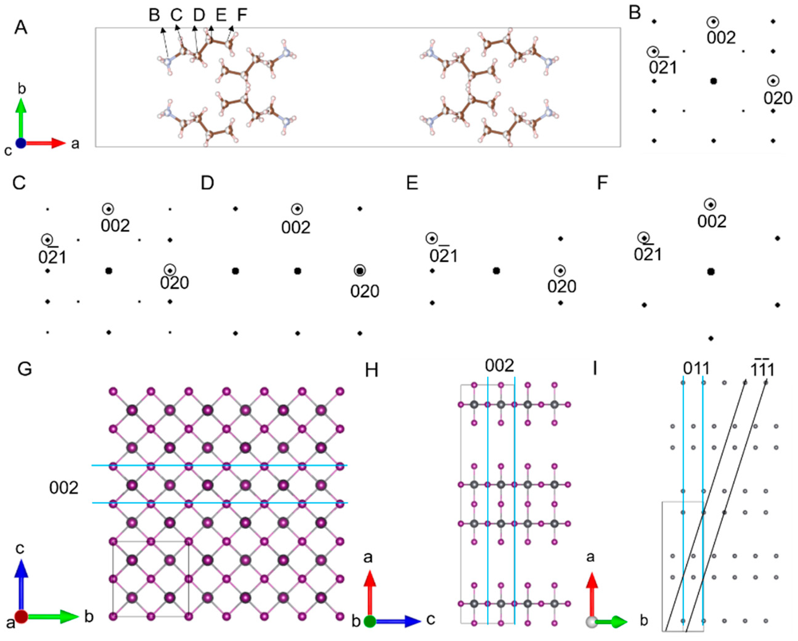
To further understand the electron irradiation-induced structural damage, structure-diffraction relationship is analyzed in detail. For such purpose, the original structure is decomposed into three sections: the long organic chains (BA+), the short organic cations (MA+/FA+), and the inorganic Pb–I layer [Pb2I7]3− (Figure 3A–D). The electron diffraction from the whole structure can be considered as the summation of diffraction from each section along [100] the zone axis, whose projections are shown in Figure 3F–I. The initial disappeared spots correspond to (01) planes, indicating the atoms in the (01) planes vanished or moved away under the electron beam. As shown in Figure 3L,N, both the BA+ section and the [Pb2I7]3− section contribute to the (01) spot. For the former, given that the nitrogen atom and three out of four carbon atoms in the BA+ section are on the (01) plane (Figure 4A–F), the movements of carbon/nitrogen atoms make the long organic chains disorder and even break them into pieces. Regarding the latter, the original corner-shared octahedrons are tilted, which is exactly the reason for that the I atom columns lie in the (01) plane but not the (00) plane (Figure 3I). If the (01) spots first disappear, it is simply because electron beam breaks the bonds between Pb and I, the whole skeletons of Pb–I octahedron might be collapsed and thus the low frequency information, i.e., the nearest (1) spot (6 Å) should also disappear. Apparently, it is not the case experimentally. As such, it could be more plausible that the originally tilted octahedrons convert to non-tilted octahedrons, the I atom scattering contributes less to (01) spots and more to the (002)/(020) spots (Figure 3D,E,I,J,N,O). Therefore, as for the structural collapse, the long organic chains (BA+) are more vulnerable and could be damaged prior to the collapse of [Pb2I7]3− skeletons. On this basis, even though the long organic chains are first damaged, the Pb–I octahedrons have not yet collapsed so that the HRTEM image still stays uniform (Figure 2A). With continuous electron irradiation, the fading FT spots corresponding to (), (), and () planes are denoted by three black circles in Figure 3M,O, which suggests that all the MA+/FA+, and [Pb2I7]3− sections are gradually damaged. To be noted that although those three spots also exist in Figure 3L, it is believed that the BA+ section has already been damaged in the first step, and therefore it is not considered anymore. The last disappeared (1) and (111) spots correspond to the MA+/FA+ section and also the [Pb2I7]3− section (Figure 4I). Specifically, the (0) and () spots are vanished prior to the (11) and (1) spots. As shown in Figure 4G,H, the () plane corresponds to the lattice plane of I atom columns, implying that partial Pb–I bonds are destroyed by the electron beam. After all the organic groups damaged and partial Pb–I bonds broken, the [Pb2I7]3− skeletons collapse at the end, resulting in the decomposed product of other phase such as PbI2 (Figure 2C).
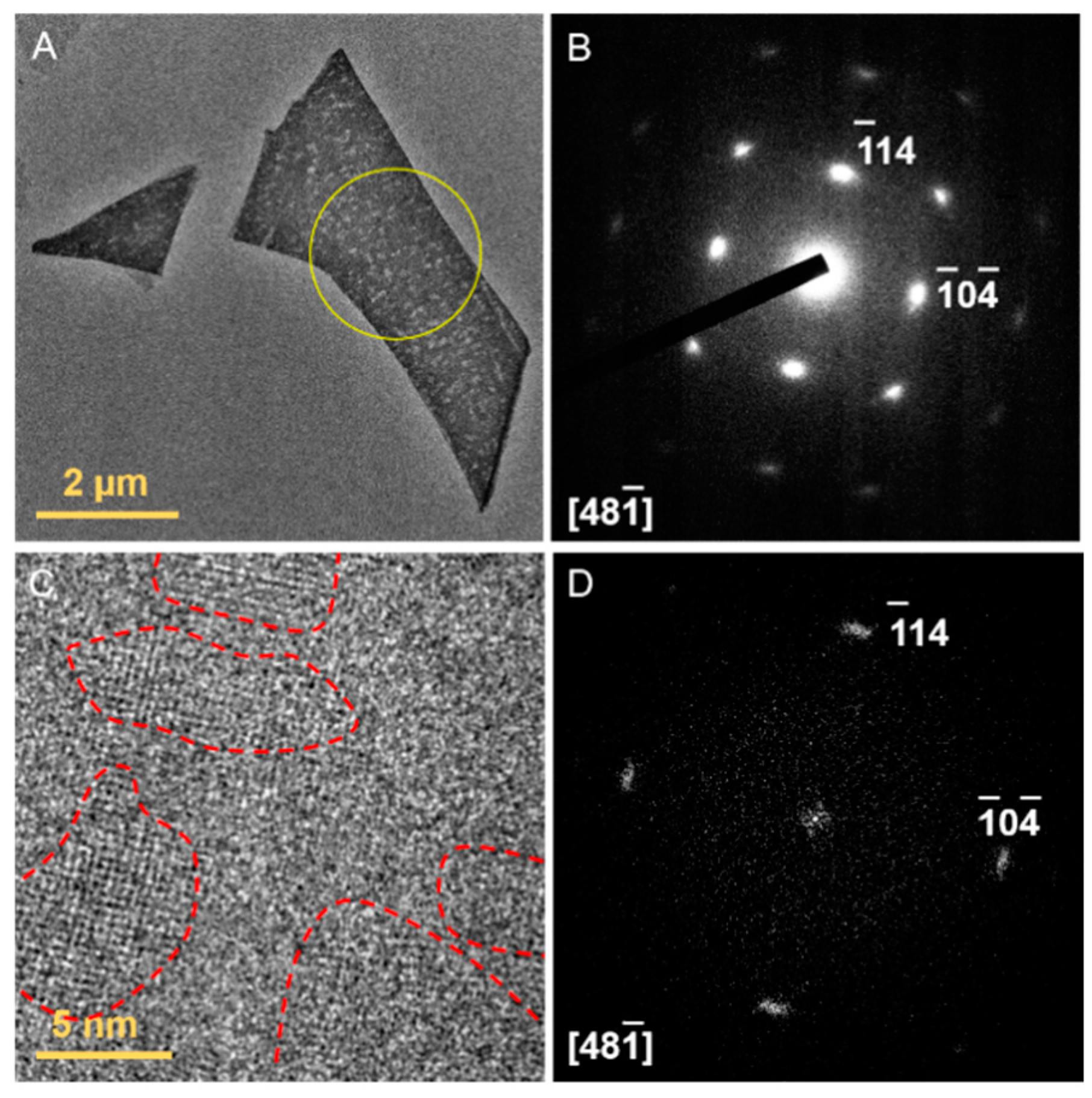
Next, the structural damage in moist air was investigated. The low magnification image of an air-degraded sample is shown in Figure 5A, and porous feature could be observed compared to well-preserved sample (Figure 1B). The SAED pattern and FT of the HRTEM image show that the interplanar spacing of the damaged sample matches well with that of PbI2 (Figure 5B,D and Figure 2G), suggesting that degraded structure in moist air is the same as the damaged structure under the electron beam. The difference is that the degraded crystalline domain is smaller in moist air (approximately 5~10 nm) (Figure 5C).
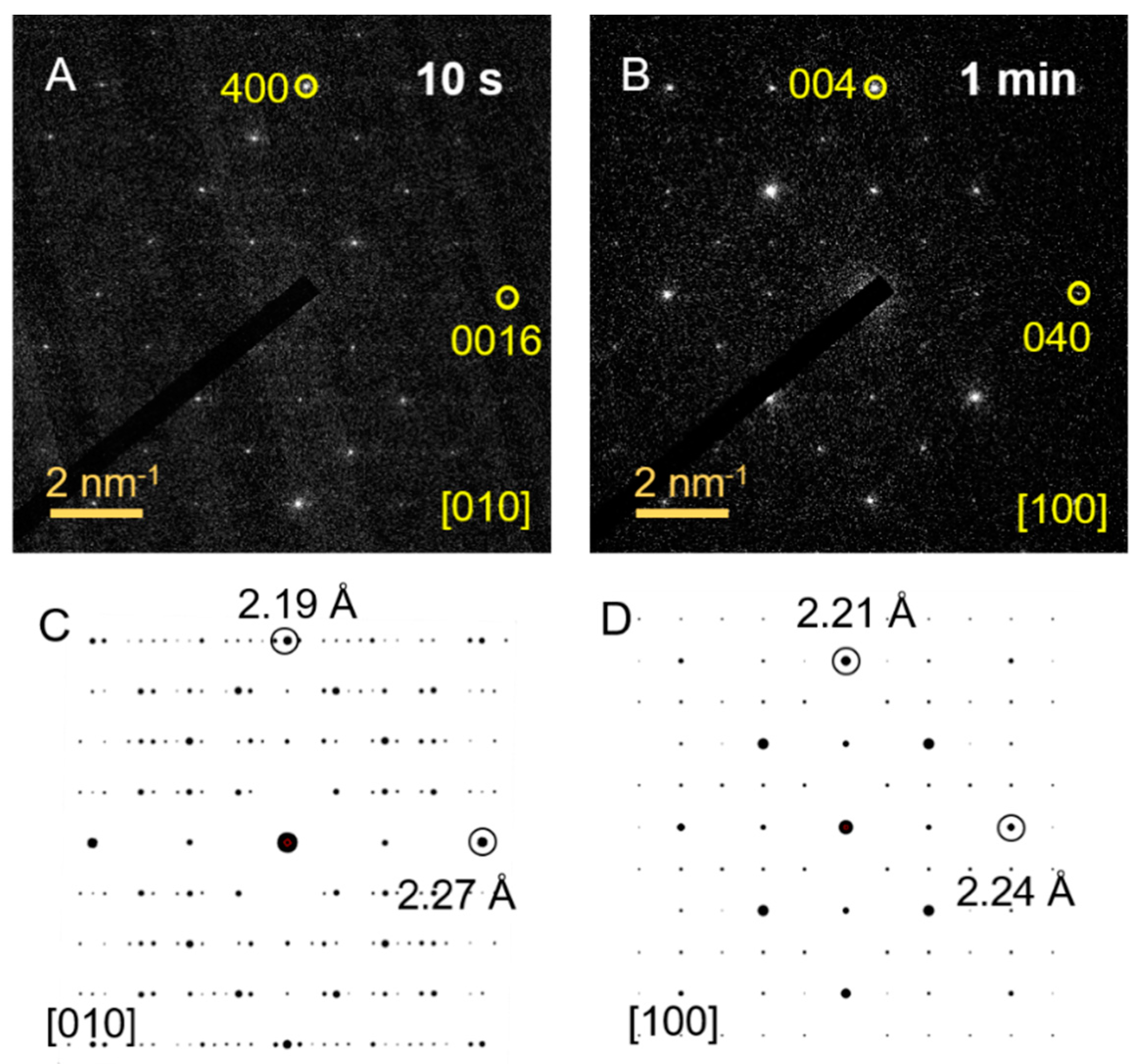
Finally, the temperature effect was evaluated. It is almost becoming a common sense that lowering the temperature could protect irradiation sensitive samples from being damage, especially for materials containing organic components [15]. In principle, low temperature does slow down the atom movements and hence prolong the stable time for the intrinsic structure. Nevertheless, we would like to remind that the liquid nitrogen condition is not suitable for all sensitive materials, and one should be careful if there is phase transformation at lower temperature. Here the BA2FAPb2I7 sheet (Figure 6A) is an example. When lowering the temperature to liquid nitrogen temperature, satellite diffraction spots appear in the diffraction pattern of BA2FAPb2I7 around the main diffraction spots (Figure 6B and Figure 7A), being consistent with the simulated SAED of low temperature BA2FAPb2I7 structure (solved at 150 K) (Figure 7A,C) [16]. This structure is different from the room temperature structure (Figure 1C). Even keeping at liquid nitrogen temperature, structural damage could occur if electron irradiation accumulates to certain amount. The SAED pattern after 2 min irradiation (the accumulative dose reaches to about 5 e− Å−2) is shown in Figure 6C. Although the pattern looks similar with Figure 6B, the lattice distance has already been changed slightly (Figure 7). It is indexed to be a different structure in different zone axis, and it is quite similar with the room temperature case (Figure 1C). The phase transformation could be understood as illustrated in Figure 6D–F. The low temperature is monoclinic structure (Figure 6E) while the room temperature is orthorhombic (Figure 6D). The low temperature structure can be considered as the room temperature structure shearing along the plane parallel to Pb–I layer and contracting along the direction perpendicular to Pb–I layer (Figure 6F). Under the electron irradiation, BA2FAPb2I7 transits gradually from monoclinic to orthorhombic structure. For the case of BA2MAPb2I7, similar phenomenon was also observed.
3. Discussion
The report first investigated the structure of BA2FAPb2I7 and BA2MAPb2I7. Their diffraction patterns at room temperature resemble each other in the lattice distance and geometry of diffraction spots, which is consistent with their similar optical and electronic properties. Beam damage process is analyzed in reciprocal space. A general conclusion is that the organic groups suffer from structural collapse in a short time. The A-site organic cations are bounded to [BX6]4− octahedrons by hydrogen bonds, and the [B2X7]3− layer and the organic-chain layer are bonded by weaker Van Der Waals force. From the standpoint of interactions between the three sections as in Figure 3, we found a correlation between the sequence of structural destruction and the strength of interaction. The long organic chains are the most sensitive and vulnerable section because of their weak Van Der Waals force with [B2X7]3− layer. After the organic-chain layer disordered, further electron irradiation causes damage to the short organic cations, and finally the inorganic layers and entire framework of the structure collapses into small particles. Likewise, in regard to the instability of perovskites to moisture, the structure destruction could be understood in the same manner. As for the resultant products for halide perovskite destruction, agreement has not been achieved yet in the community. This report demonstrates the similar resultant PbI2 particles produced in moist air and under electron irradiation, which provides a hint of their inner-link in the damage mechanism. In contrast, an early report did not detect obvious PbI2 under low acceleration voltage (1–5 kV) by cathodoluminescence spectroscopy analysis [17]. In our comparison experiments, PbI2 particles were not observed at 80 kV TEM either. Therefore, the resultant products may be case-dependent and there might not be a versatile damage pathway. Meanwhile, our structure evolution studied here can be supported by the recent report where the 2D perovskites were illuminated by ultraviolet light and white light [18]. Our method of structural analysis demonstrated here provides a reliable way to evaluate the damage process. Finally, the low temperature experiments indicate that some beam sensitive materials may not be suitable to go for cryo-TEM, and it is recommended checking carefully if phase transformation will occur at low temperature.
4. Materials and Methods
4.1. Synthesis of BA2FAPb2I7 and BA2MAPb2I7
All the samples were synthesized via the solution method [16]. PbO powders, hydroiodic acid (HI, 57 wt % in H2O), hypophosphorous acid (H3PO2, 50 wt % in H2O) were purchased from Sigma Aldrich (St. Louis, MO, USA), while methylammonium iodide (MAI), formamidinium iodide (FAI), and n-butylammonium iodide (BAI) were purchased from Greatcell Solar Ltd (Elanora, Australia). All precursors were used as received. Firstly, PbO (0.59 mmol), BAI (0.43 mmol), and MAI or FAI (0.31 mmol) precursors were dissolved in HI (0.9 mL)/H3PO2 (0.1 mL) in a 10 mL glass vial. With magnet stirring, the vial was heated to 120 °C in oil bath. When the all precursors got completely dissolved, the solution became transparent. Then the stirring was terminated. After that, the solution was cooled down at a rate of 10 °C/5 min, during which the crystals were formed gradually. The final products were collected by vacuum infiltration and the residue solvent was removed in a vacuum chamber.
4.2. TEM Sample Preparation
2D halide perovskite nanosheets were obtained by mechanical exfoliating from single crystals. The weak adhesive tapes used for exfoliation were then dipped into chlorobenzene so that the perovskite samples could be separated and transferred onto TEM grids. The whole process was accomplished in an argon-filled glove box. After drying in glove box, the TEM grids were quickly taken out and inserted into the microscope vacuum chamber, minimizing the exposure to air. The exposure time was estimated to be less than two minutes.
4.3. X-ray Diffraction and TEM Characterization
The XRD data were collected by a Rigaku Smart Lab using a Cu Kα source (λ = 1.540 56 Å). The TEM study was carried out on with a 200 kV JEM-2100plus (JEOL Ltd., Tokyo, Japan). The images were acquired with a TVIPS camera (TEMCam-XF416, TVIPS, Gauting, Germany). The cooling experiment was performed using Gatan 914.6 cooling holder (Gatan, Pleasanton, CA, USA). The dose-rate was controlled by varying electron beam spot size and adjusting brightness of the electron beam. The dose-rate was much less than 1 e− Å−2 s−1 when acquiring selected area electron diffraction (SAED) patterns and low magnification images. The HRTEM imaging were performed at 200 kV with the electron dose-rate of 50~180 e− Å−2 s−1. Given that the specimen is sensitive to electrons, the defocus was determined at adjacent area of the specimen. Then the electron beam was turned off and the specimen was moved to the center of fluorescent screen. The electron beam was turned on again and at the same time the camera started to acquire single images or image series.
4.4. Structure Model
All the model demonstrations are drawn using VESTA [19]. All the kinematical SAED patterns were simulated with MacTempasX (version 2.4.48, Roar Kilaas, BerKeley, CA, USA).
5. Conclusions
Structural damage of 2D organic–inorganic halide perovskites was studied by using BA2FAPb2I7 and BA2MAPb2I7 as examples. The combination of SAED and HRTEM analysis reveals the structure evolution under the electron irradiation and moisty environment. Organic–inorganic halide perovskites are so beam sensitive that even low dose-rate electrons are detrimental to the structure. Electron irradiation first impacts the long organic chains, then destroys the short organic cations and the inorganic skeletons, and finally breaks the uniform structure into small particles of other phases. Degradation under moisty environment is similar with that under the electron irradiation. Additionally, the structure undergoes a phase transformation at low temperature and low temperature structure is still sensitive to the electron irradiation. The structure analysis provided here may be helpful for future development of stable halide perovskite materials for various applications.
Supplementary Materials
The following are available online at https://0-www-mdpi-com.brum.beds.ac.uk/2304-6740/8/2/13/s1, Table S1: Single crystal X-ray diffraction data of BA2MAPb2I7. Figure S1: Raw HRTEM series and its FT images show the structural change under electron beam.
Author Contributions
Methodology, B.Y. and Y.Y.; TEM experiments and data curation, B.Y.; materials synthesis, E.S. and L.D.; writing—original draft preparation, B.Y.; writing—review and editing, B.Y., E.S., C.L., and Y.Y.; supervision, Y.Y. All authors have read and agreed to the published version of the manuscript.
Funding
This work was supported by the startup funding from ShanghaiTech University, the National Natural Science Foundation of China (21805184), the Natural Science Foundation of Shanghai (18ZR1425200).
Acknowledgments
The TEM characterization was supported by the Center for High-resolution Electron Microscopy (CћEM) at ShanghaiTech University. L. Dou and E. Shi thank the support from Davidson School of Chemical Engineering of Purdue University.
Conflicts of Interest
The authors declare no conflict of interest.
Abbreviations
The following abbreviations are used in this manuscript:
| HRTEM | high-resolution transmission electron microscopy |
| FT | Fourier transform |
| SAED | selected area electron diffraction |
References
- Manser, J.S.; Christians, J.A.; Kamat, P.V. Intriguing optoelectronic properties of metal halide perovskites. Chem. Rev. 2016, 116, 12956–13008. [Google Scholar] [CrossRef] [PubMed]
- Dou, L.; Wong, A.B.; Yu, Y.; Lai, M.; Kornienko, N.; Eaton, S.W.; Fu, A.; Bischak, C.G.; Ma, J.; Ding, T.; et al. Atomically thin two-dimensional organic–inorganic hybrid perovskites. Science 2015, 349, 1518–1521. [Google Scholar] [CrossRef] [PubMed] [Green Version]
- Li, M.H.; Yeh, H.H.; Chiang, Y.H.; Jeng, U.S.; Su, C.J.; Shiu, H.W.; Hsu, Y.J.; Kosugi, N.; Ohigashi, T.; Chen, Y.A.; et al. Highly Efficient 2D/3D Hybrid Perovskite Solar Cells via Low-Pressure Vapor-Assisted Solution Process. Adv. Mater. 2018, 30, e1801401. [Google Scholar] [CrossRef] [PubMed]
- Lee, J.W.; Dai, Z.; Han, T.H.; Choi, C.; Chang, S.Y.; Lee, S.J.; De Marco, N.; Zhao, H.; Sun, P.; Huang, Y.; et al. 2D perovskite stabilized phase-pure formamidinium perovskite solar cells. Nat. Commun. 2018, 9, 3021. [Google Scholar] [CrossRef] [PubMed] [Green Version]
- Correa-Baena, J.P.; Abate, A.; Saliba, M.; Tress, W.; Jacobsson, T.J.; Gratzel, M.; Hagfeldt, A. The rapid evolution of highly efficient perovskite solar cells. Energy Environ. Sci. 2017, 10, 710–727. [Google Scholar] [CrossRef]
- Yu, Y.; Zhang, D.; Kisielowski, C.; Dou, L.; Kornienko, N.; Bekenstein, Y.; Wong, A.B.; Alivisatos, A.P.; Yang, P. Atomic Resolution Imaging of Halide Perovskites. Nano Lett. 2016, 16, 7530–7535. [Google Scholar] [CrossRef] [PubMed] [Green Version]
- Yu, Y.; Zhang, D.; Yang, P. Ruddlesden–Popper Phase in Two-Dimensional Inorganic Halide Perovskites: A Plausible Model and the Supporting Observations. Nano Lett. 2017, 17, 5489–5494. [Google Scholar] [CrossRef] [PubMed] [Green Version]
- Urban, K.W. Studying atomic structures by aberration-corrected transmission electron microscopy. Science 2008, 321, 506–510. [Google Scholar] [CrossRef] [PubMed] [Green Version]
- Christians, J.A.; Miranda Herrera, P.A.; Kamat, P.V. Transformation of the excited state and photovoltaic efficiency of CH3NH3PbI3 perovskite upon controlled exposure to humidified air. J. Am. Chem. Soc. 2015, 137, 1530–1538. [Google Scholar] [CrossRef] [PubMed]
- Sichert, J.A.; Tong, Y.; Mutz, N.; Vollmer, M.; Fischer, S.; Milowska, K.Z.; García Cortadella, R.; Nickel, B.; Cardenas-Daw, C.; Stolarczyk, J.K.; et al. Quantum Size Effect in Organometal Halide Perovskite Nanoplatelets. Nano Lette. 2015, 15, 6521–6527. [Google Scholar] [CrossRef] [PubMed]
- Tong, Y.; Bladt, E.; Aygüler, M.F.; Manzi, A.; Milowska, K.Z.; Hintermayr, V.A.; Docampo, P.; Bals, S.; Urban, A.S.; Polavarapu, L.; et al. Highly Luminescent Cesium Lead Halide Perovskite Nanocrystals with Tunable Composition and Thickness by Ultrasonication. Angew. Chem. Int. Ed. 2016, 55, 13887–13892. [Google Scholar] [CrossRef]
- Dang, Z.; Shamsi, J.; Palazon, F.; Imran, M.; Akkerman, Q.A.; Park, S.; Bertoni, G.; Prato, M.; Brescia, R.; Manna, L. In Situ Transmission Electron Microscopy Study of Electron Beam-Induced Transformations in Colloidal Cesium Lead Halide Perovskite Nanocrystals. ACS Nano 2017, 11, 2124–2132. [Google Scholar] [CrossRef] [Green Version]
- Mitchell, D.R.G. HRTEM Filter V4.0. Available online: http://www.dmscripting.com/hrtem_filter.html (accessed on 1 November 2019).
- Wyckoff, R.W.G. Crystal Structures, 2nd ed.; Interscience Publishers: New York, NY, USA, 1963; Volume 1, pp. 239–444. [Google Scholar]
- Li, Y.; Li, Y.; Pei, A.; Yan, K.; Sun, Y.; Wu, C.L.; Joubert, L.M.; Chin, R.; Koh, A.L.; Yu, Y.; et al. Atomic structure of sensitive battery materials and interfaces revealed by cryo-electron microscopy. Science 2017, 358, 506–510. [Google Scholar] [CrossRef] [PubMed] [Green Version]
- Shi, E.; Deng, S.; Yuan, B.; Gao, Y.; Akriti; Yuan, L.; Davis, C.S.; Zemlyanov, D.; Yu, Y.; Huang, L.; et al. Extrinsic and Dynamic Edge States of Two-Dimensional Lead Halide Perovskites. ACS Nano 2019, 13, 1635–1644. [Google Scholar] [CrossRef] [PubMed]
- Xiao, C.; Li, Z.; Guthrey, H.; Moseley, J.; Yang, Y.; Wozny, S.; Moutinho, H.; To, B.; Berry, J.J.; Gorman, B.; et al. Mechanisms of Electron-Beam-Induced Damage in Perovskite Thin Films Revealed by Cathodoluminescence Spectroscopy. J. Phys. Chem. C 2015, 119, 26904–26911. [Google Scholar] [CrossRef]
- Nie, L.; Ke, X.; Sui, M. Microstructural Study of Two-Dimensional Organic–Inorganic Hybrid Perovskite Nanosheet Degradation under Illumination. Nanomaterials 2019, 9, 722. [Google Scholar] [CrossRef] [PubMed] [Green Version]
- Momma, K.; Izumi, F. VESTA 3 for three-dimensional visualization of crystal, volumetric and morphology data. J. Appl. Crystallogr. 2011, 44, 1272–1276. [Google Scholar] [CrossRef]
Figure 1.
(A) Structural schematic of layered perovskite BA2FAPb2I7/BA2MAPb2I7 where partial organic chains are not shown for clear demonstration; (B) low magnification image of 2D BA2FAPb2I7 sheets and its corresponding SAED in (C). (D) average background subtraction filtered (ABSF) high-resolution transmission electron microscopy (HRTEM) image of BA2FAPb2I7 along [100] zone axis.

Figure 2.
Structural evolution of a BA2FAPb2I7 sheet under the electron beam. (A–C) ABSF-filtered HRTEM images obtained at T0, T0+1 s and T0+2 s. The exposure time of each frame is 200 ms. The crystalline region in (C) is outlined by a white line. (D) Enlarged HRTEM image of the boxed region in (C). Inset is the [48] structural projection of Rm PbI2 (Pb: green; I: red). (E–G) Corresponding FT of HRTEM images shown in (A–C) respectively. The yellow arrows and dot circles mark the disappeared spots during the electron irradiation. The index is based on perfect structure of BA2(MA/FA)Pb2I7 solved at 310 K. (H) Simulated kinematical selected-area electron diffraction (SAED) pattern of [48] PbI2.

Figure 3.
The structural model of BA2(MA/FA)Pb2I7 (A), BA+ (B), MA+/FA+ (C), tilted [Pb2I7]3− (D), and non-tilted [Pb2I7]3− (E). (F–J) The corresponding structural projection along [100] direction in A–D. The (01) planes are depicted by dot lines. (K–O) Simulated SAED patterns of BA2(MA/FA)Pb2I7, BA+ section, MA+/FA+ section, tilted [Pb2I7]3− section, and non-tilted [Pb2I7]3−, respectively. The red circle indicates the missing ( plane in the MA+/FA+ section. Ⅰ, Ⅱ, and Ⅲ denote the spot disappearance order under electron irradiation.

Figure 4.
(A) The structural projection of the BA+ section in [001] direction. (B–F) Corresponding simulated electron diffraction of the frameworks from different nitrogen/carbon atoms. Gray and brown represent nitrogen and carbon atoms, respectively. (G,H) The structural projections of non-tilted [Pb2I7]3− section in [] and [] direction, respectively. The blue lines represent the (002) plane. (I) The structural projection of Pb atoms in [] direction. The blue line and the black line represent the (011) and () plane.

Figure 5.
Characterization of an air-damaged sample. (A) Low magnification image of damaged sample and (B) its corresponding SAED, the yellow circle in (A) denotes the selected area; (C) The HRTEM image and (D) its corresponding FT pattern. The red dot lines outline the particles of PbI2.
Figure 5.
Characterization of an air-damaged sample. (A) Low magnification image of damaged sample and (B) its corresponding SAED, the yellow circle in (A) denotes the selected area; (C) The HRTEM image and (D) its corresponding FT pattern. The red dot lines outline the particles of PbI2.

Figure 6.
Low temperature structural evolution as electron irradiation accumulates. (A) Low magnification image of BA2FAPb2I7 at liquid nitrogen temperature. (B) SAED pattern when the electron irradiation time is less than 1 min; the inset highlights the diffraction spot with satellite spots. (C) SAED pattern when the electron irradiation time is approximately 2 min; the inset highlights the diffraction spot without satellite spots. The electron dose-rate is approximately 0.05 e− Å−2 s−1. (D) Room temperature structure in [100] projection. (E) Low temperature structure in [010] projection. (F) Schematic of the structure evolution.

Figure 7.
Diffraction evolution as electron irradiation accumulates. (A,B) SAED acquired when the sample is exposed to electron beam after 10 s and 1 min respectively. (C) Simulated kinematical SAED pattern of low temperature BA2FAPb2I7 structure, which is solved at 150 K. (D) Simulated kinematical SAED pattern of BA2MAPb2I7, which is solved at 310 K.

© 2020 by the authors. Licensee MDPI, Basel, Switzerland. This article is an open access article distributed under the terms and conditions of the Creative Commons Attribution (CC BY) license (http://creativecommons.org/licenses/by/4.0/).
Share and Cite
MDPI and ACS Style
Yuan, B.; Shi, E.; Liang, C.; Dou, L.; Yu, Y. Structural Damage of Two-Dimensional Organic–Inorganic Halide Perovskites. Inorganics 2020, 8, 13. https://0-doi-org.brum.beds.ac.uk/10.3390/inorganics8020013
AMA Style
Yuan B, Shi E, Liang C, Dou L, Yu Y. Structural Damage of Two-Dimensional Organic–Inorganic Halide Perovskites. Inorganics. 2020; 8(2):13. https://0-doi-org.brum.beds.ac.uk/10.3390/inorganics8020013
Chicago/Turabian StyleYuan, Biao, Enzheng Shi, Chao Liang, Letian Dou, and Yi Yu. 2020. "Structural Damage of Two-Dimensional Organic–Inorganic Halide Perovskites" Inorganics 8, no. 2: 13. https://0-doi-org.brum.beds.ac.uk/10.3390/inorganics8020013
Note that from the first issue of 2016, this journal uses article numbers instead of page numbers. See further details here.