Graphene Nanoribbon as Potential On-Chip Interconnect Material—A Review


1
Department of Electrical & Electronics Engineering, Birla Institute of Technology & Science (BITS), Pilani 333031, India
2
Department of Physics &Materials Science, Jaypee University of Information Technology (JUIT), Solan 173234, India
*
Author to whom correspondence should be addressed.
C 2018, 4(3), 49; https://0-doi-org.brum.beds.ac.uk/10.3390/c4030049
Submission received: 29 July 2018
/
Revised: 15 August 2018
/
Accepted: 16 August 2018
/
Published: 30 August 2018
Abstract
:In recent years, on-chip interconnects have been considered as one of the most challenging areas in ultra-large scale integration. In ultra-small feature size, the interconnect delay becomes more pronounced than the gate delay. The continuous scaling of interconnects introduces significant parasitic effects. The resistivity of interconnects increases because of the grain boundary scattering and side wall scattering of electrons. An increased Joule heating and the low current carrying capability of interconnects in a nano-scale dimension make it unreliable for future technology. The devices resistivity and reliability have become more and more serious problems for choosing the best interconnect materials, like Cu, W, and others. Because of its remarkable electrical and its other properties, graphene becomes a reliable candidate for next-generation interconnects. Graphene is the lowest resistivity material with a high current density, large mean free path, and high electron mobility. For practical implementation, narrow width graphene sheet or graphene nanoribbon (GNR) is the most suitable interconnect material. However, the geometric structure changes the electrical property of GNR to a small extent compared to the ideal behavior of graphene film. In the current article, the structural and electrical properties of single and multilayer GNRs are discussed in detail. Also, the fabrication techniques are discussed so as to pattern the graphene nanoribbons for interconnect application and measurement. A circuit modeling of the resistive-inductive-capacitive distributed network for multilayer GNR interconnects is incorporated in the article, and the corresponding simulated results are compared with the measured data. The performance of GNR interconnects is discussed from the view of the resistivity, resistive-capacitive delay, energy delay product, crosstalk effect, stability analysis, and so on. The performance of GNR interconnects is well compared with the conventional interconnects, like Cu, and other futuristic potential materials, like carbon nanotube and doped GNRs, for different technology nodes of the International Technology Roadmap for Semiconductors (ITRS).
1. Introduction
The rapid miniaturization of the transistor feature size in an integrated circuit chip has been observed over the past four decades. With the introduction of nano-scale technology, the intrinsic gate delay of the transistor has become less significant compared to the interconnects delay [1,2]. So, the chip performance and reliability are better determined by the properties of the interconnects instead of the transistors [3,4]. In a not so small sub-micron range, the interconnects are approximated as a lumped resistive-capacitive (RC) network, whereas in the nano-scale range, a distributed resistive-inductive-capacitive (RLC) network is the more appropriate model [5,6]. In reality, interconnects are in very close proximity to other interconnects, either in same or different levels in a chip. So, the complex geometry of the integrated circuit introduces resistive, capacitive, and inductive parasitic components, which have different effects on circuit behavior, like (i) large propagation delay, (ii) more dynamic power dissipation, and (iii) high cross-talk effect [3,4,7,8].
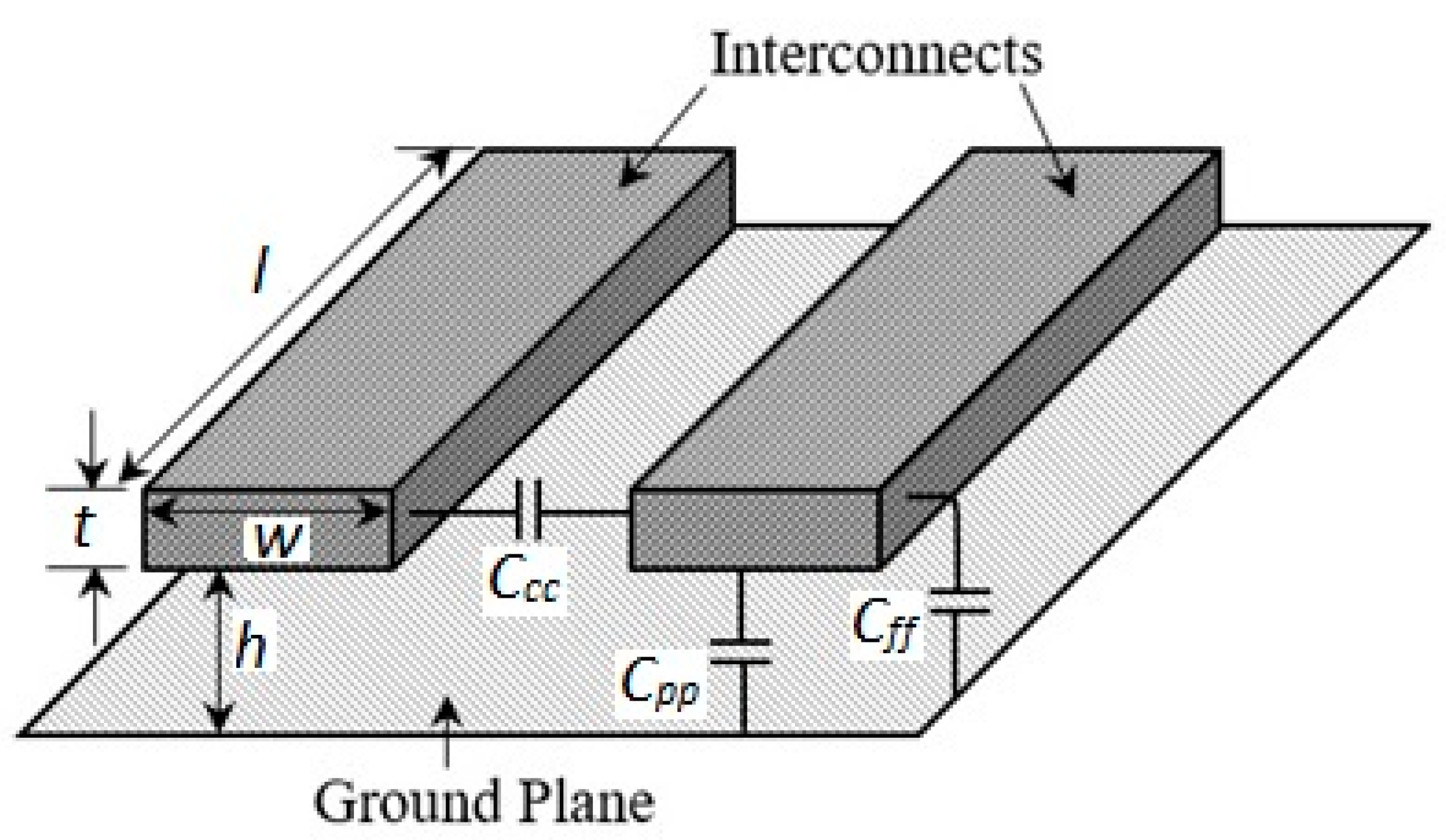
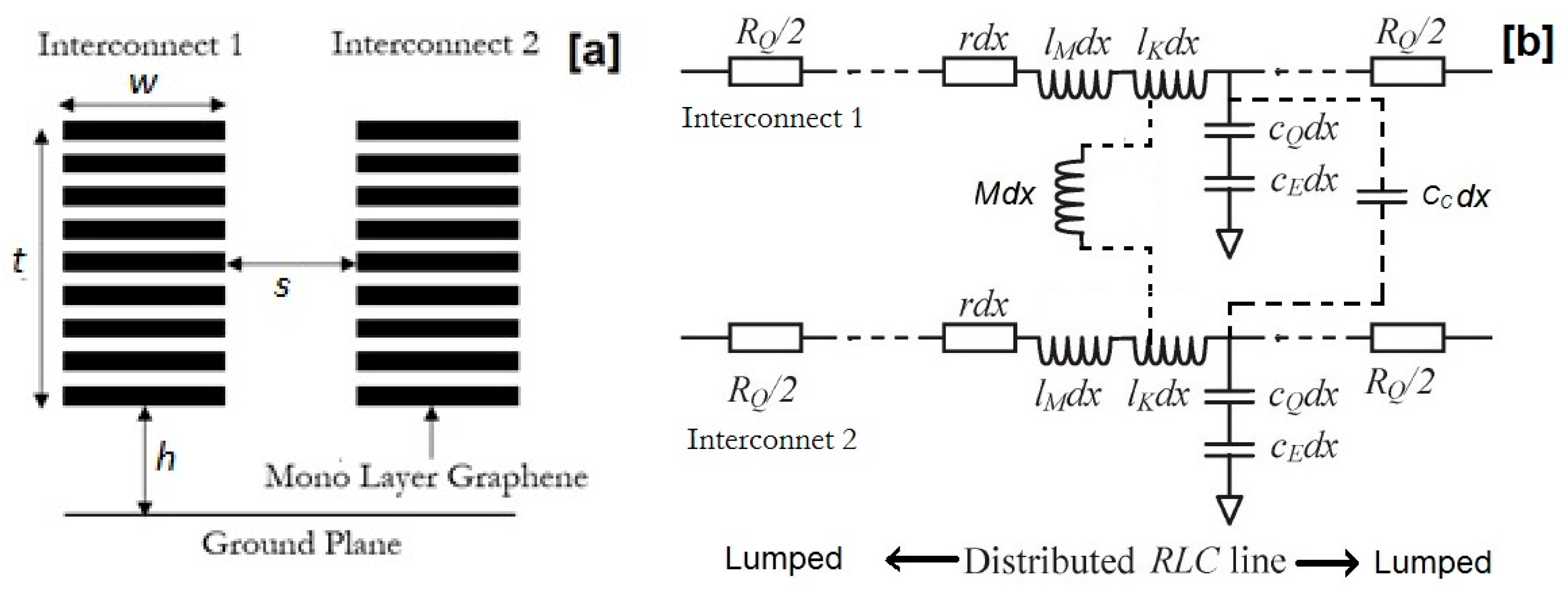
The capacitance of on-chip interconnect principally depends on its shape (for rectangular interconnects: length, l; width, w; and thickness, t), distance from substrate (h), dielectric constant of the surrounding environment (εr), and distance from the adjacent interconnects, as shown in Figure 1. The use of a lower permittivity material, like aero gels (εr ≈ 1.5), instead of SiO2 (εr ≈ 4) may offer a lower capacitance. However, new dielectric materials may not be suitable for large scale fabrication. However, the structural parameters of the interconnects become shorter with geometrical scaling, which increases the fringing field capacitance (Cff) over the parallel plate capacitance (Cpp). When small values of w lead to denser wiring and less area overhead, a smaller w/h (<1) contributes a very high value of Cff, thereby increasing the overall interconnect capacitance. The shorter length of the interconnects is also responsible for a high Cff. So, in a nano-scale region, the overall interconnect capacitance (Cint = Cpp + Cff) increases because of an enhanced fringing field effect. The capacitive coupling (Ccc) between the neighboring interconnect lines is responsible for the signal crosstalk related problem. Ccc becomes very significant when the thickness (t) of the interconnects is comparable to its width (w). So, structural miniaturization contributes a high capacitance for on-chip interconnects.
The resistance of on-chip interconnects depends on its shape and resistivity (ρ). So far as the resistivity is concerned, Cu (ρ = 1.7 × 10⁻⁸ Ωm) offers the lowest resistivity compared to Al, W, and doped polysilicon. But, in recent years, the resistivity of the Cu interconnects has increased appreciably because of the miniaturization of the interconnect dimensions that increase the carrier scattering extensively [9]. The geometrical scale down of the interconnects’ cross section becomes less or comparable than the the mean free path (MFP) of electron in the bulk metal (40 nm for Cu at room temperature) [8,10]. At the same time, the average grain size becomes much smaller than the bulk metal, resulting in the enhanced grain boundary scattering of electrons of the interconnects [3]. The International Technology Roadmap for Semiconductors (ITRS) is a set of documents produced by a group of experts, with the aim of giving a roadmap for the next 15 years. ITRS-2013 predicted that the width (w), the current density (J), and the resistivity (ρ) of the Cu interconnects would be 8 nm, 4.91 × 10⁶ A/cm2, and 10.81 × 10⁻⁸ Ωm, respectively, in the year 2027. So, the increased Joule heating will lead to the reduction of the interconnect lifetime and the overall current carrying capacity [11,12].
On the other hand, the overall dynamic power dissipation (P = CV2f, with C being the capacitance, V being the supply voltage, and f being the switching frequency) of the chip increases with the higher value of interconnects capacitance (Cint). The interconnect RC delay increases and it may become higher or comparable to the gate delay. The energy delay product (EDP) also increases significantly. Crosstalk problem becomes more pronounced in the case of dense wiring. So, the conventional interconnect metal, like Cu, may not be suitable for future-generation on-chip interconnects to overcome the critical challenges of technology scaling [1,2,3,4].
Because of its exceptionally superior electronic properties, graphene can be considered as the potentially alternative material available for on-chip interconnects. Intrinsic graphene shows the properties of semi-metal or zero gap semiconductors with excellent electronic behavior, including a high current density, high thermal conductivity, ballistic transport, mechanical robustness, and chemical inertness [13,14,15,16]. As it is already known, graphene has remarkably high electron mobility at room temperature (~15,000 cm2 V−1 S−1) [16,17] and the lowest resistivity (10−8 Ωm), almost 1.59 times smaller than silver. Because of its two-dimensional (2D) structures, graphene has limited phase space for electron scattering, and so it offers a long mean free path compared to the nano-scale metal interconnects [3,18]. Moreover, the 2D structure of the graphene sheet also offers less parasitic capacitance than the Cu interconnects [4,19]. So, these extraordinary electronic properties of graphene make it suitable for reliable on-chip interconnect material in future, with faster transport in the nanoscale regime [20,21,22,23,24].
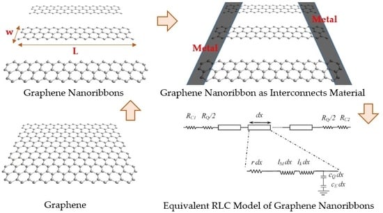
To implement graphene as a practical on-chip interconnect material, it needs to be patterned into narrow ribbon, popularly known as graphene nanoribbon (GNR). Because of its geometry (limited width), GNR shows slightly deviated electrical properties than the ideal graphene structure [25,26]. To consider graphene as the next-generation interconnect material, we should compare the interconnect properties of graphene nanoribbons (GNRs) directly to the existing on-chip interconnect materials. Considering this aspect, the current review article has been organized with the following topics. In Section 2, the basic structure of the GNR and structure dependent electrical properties have been discussed briefly. In Section 3, multiple techniques and methods have been discussed for GNRs fabrications, which are suitable for interconnect applications only. The equivalent electrical circuit model of the GNR interconnects has been discussed in Section 4. Considering the potentiality of the multilayer structure, an equivalent circuit model has been extended for multilayer graphene nanoribbons (MLGNRs) in Section 5. In Section 6, the performance of the GNR interconnects has been compared to the existing interconnect materials, like Cu, W, and other recently developed promising materials like single wall carbon nanotube (SWCNT) [27] and doped multilayered graphene nanoribbons [8,28,29,30]. In the performance comparison, issues like resistivity, capacitance, propagation delay, energy delay product, crosstalk effect, and stability analysis have been considered. Finally, Section 7 concludes the review.
2. Structural Properties of Graphene Nanoribbon (GNR)
Graphene nanoribbons (GNRs) are the single layer graphene strips with a width less than 50 nm. Superior mobility, mean free path (MFP), linear E–k relationship, and a width-dependent transport gap make GNR more appropriate for interconnect application than Cu [31,32,33,34]. Single-layer GNRs offer a lower resistance per unit length than Cu for a line width (w) less than 8 nm [35]. GNRs can be metallic or semiconducting, depending on their geometry.
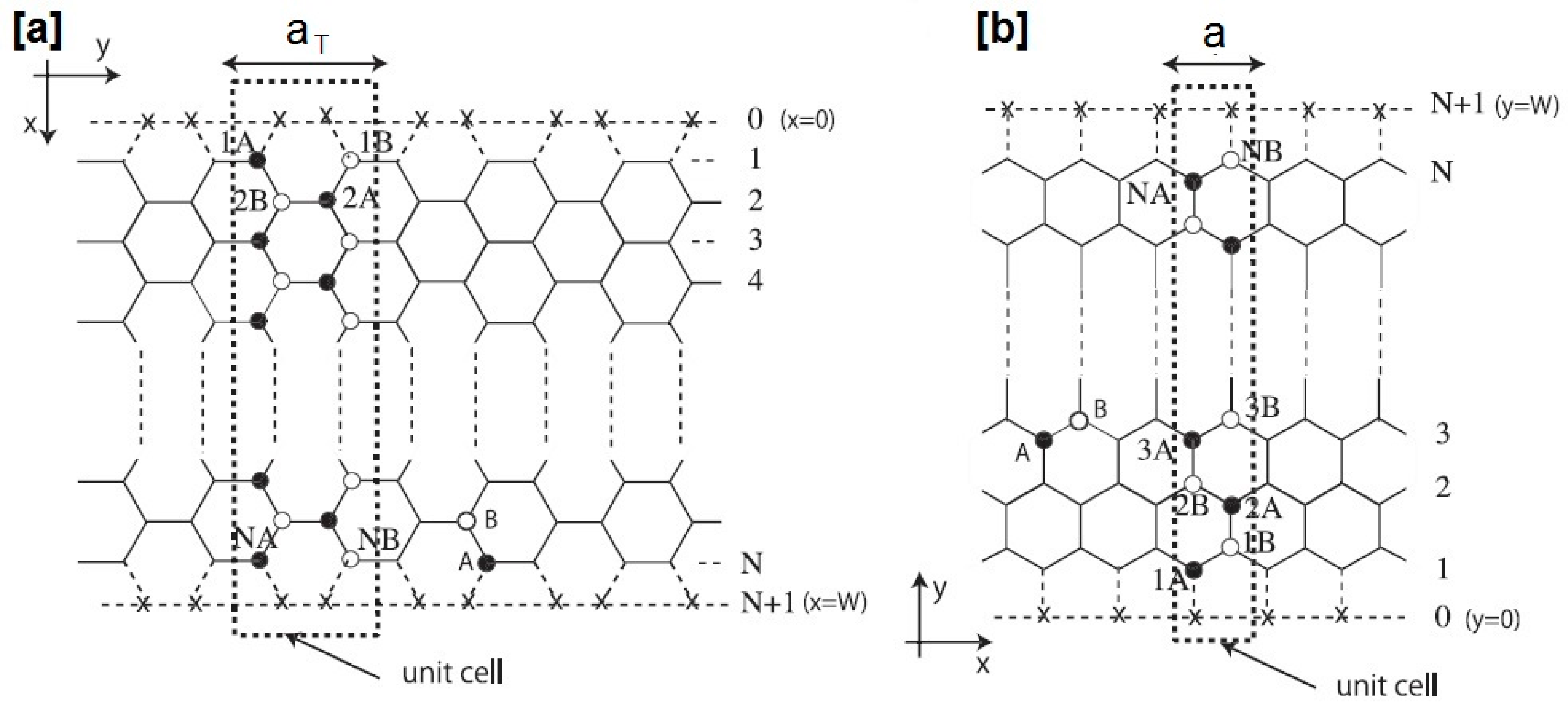
Graphene nanoribbons (GNRs) have a transverse width (w) much smaller than the longitudinal length [36,37]. There are two basic shapes in GNR, namely nanoribbons with armchair edges and nanoribbons with zigzag edges, as shown in Figure 2a,b, respectively [36,38,39]. These edges have a 30° difference in their orientation [36]. Also, the edge carbon atoms of the GNRs are passivated by hydrogen atoms and, thus, have no contribution to the electronic states near the Fermi level [38,39].
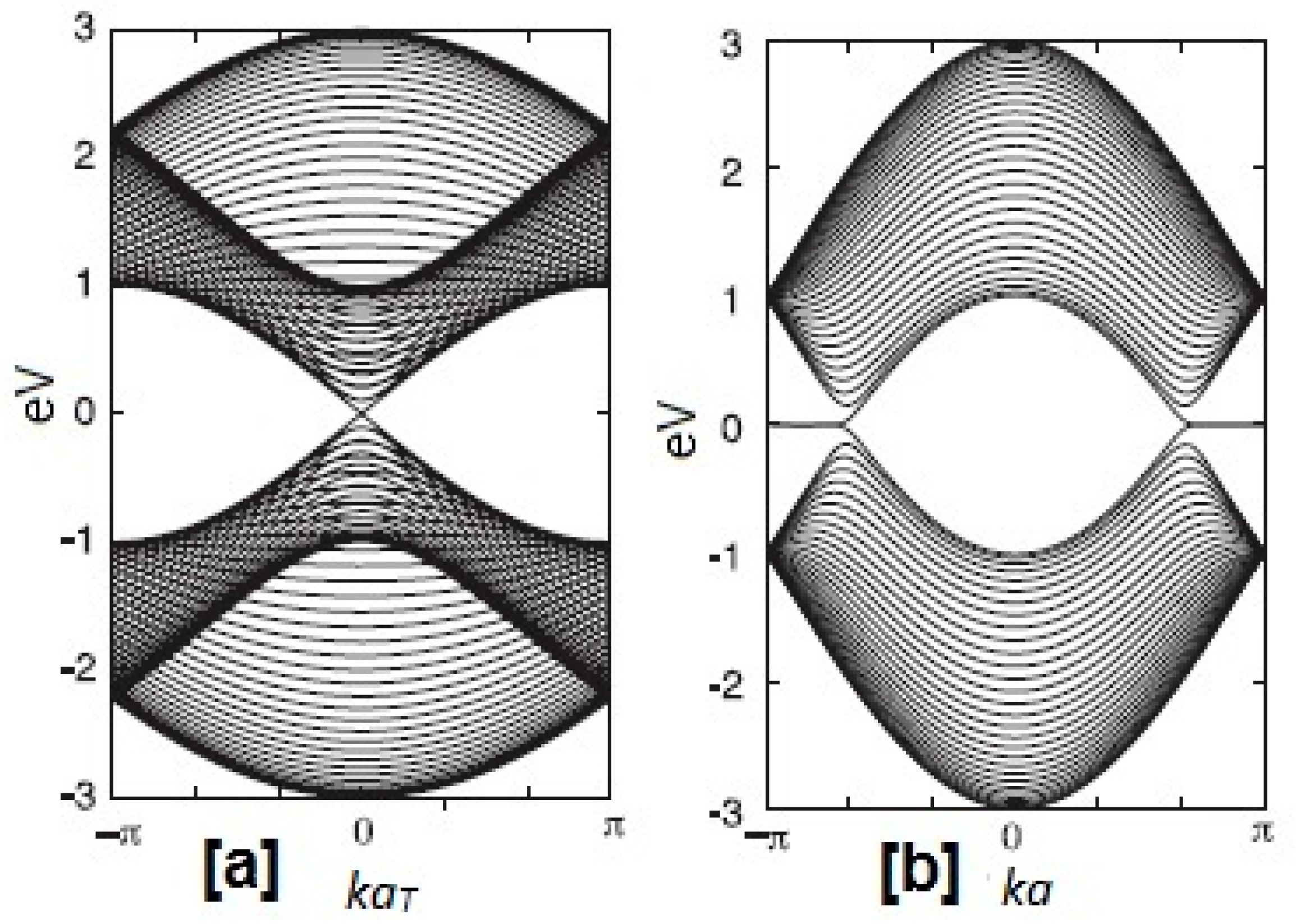
In Figure 2, N indicates the number of dimers (two carbon sites) for the armchair GNR, and the number of zigzag lines for the zigzag GNR. The width w of the graphene nanoribbon is directly related to the integer N. For the armchair GNRs, the length and width of the unit cell are aT = √3a and w = (N + 1) a/2, respectively, as shown in Figure 2a. For the zigzag GNRs, the length and width of a unit cell are a and w (w = [√3Na/2 + a/√3]), respectively, as shown in Figure 2b. The band structure projected onto the one-dimensional Brillouin zone of the armchair GNR with N = 50 is shown in Figure 3a, where the top of the valance band and the bottom of the conduction band are located at kaT = 0. An armchair GNR becomes metallic in nature if the number of carbon atoms, N, across its width is 3p + 2, and is semiconducting if N is 3p or 3p + 1, where p is an integer (p = 1, 2, 3……). For a semiconducting GNR, the band gap decreases with the increase of the GNR width, and becomes metallic at a very large value of N [24,31,40]. The zigzag GNRs onto the one-dimensional Brillouin zone have partially flat bands, because of their edge states and hence the band gaps are always zero with metallic behavior [5,38,39]. Figure 3b shows band structure of zigzag GNR for N = 30, where the top of the valance band and the bottom of the conduction band are degenerating at ka = π [24,31,38].
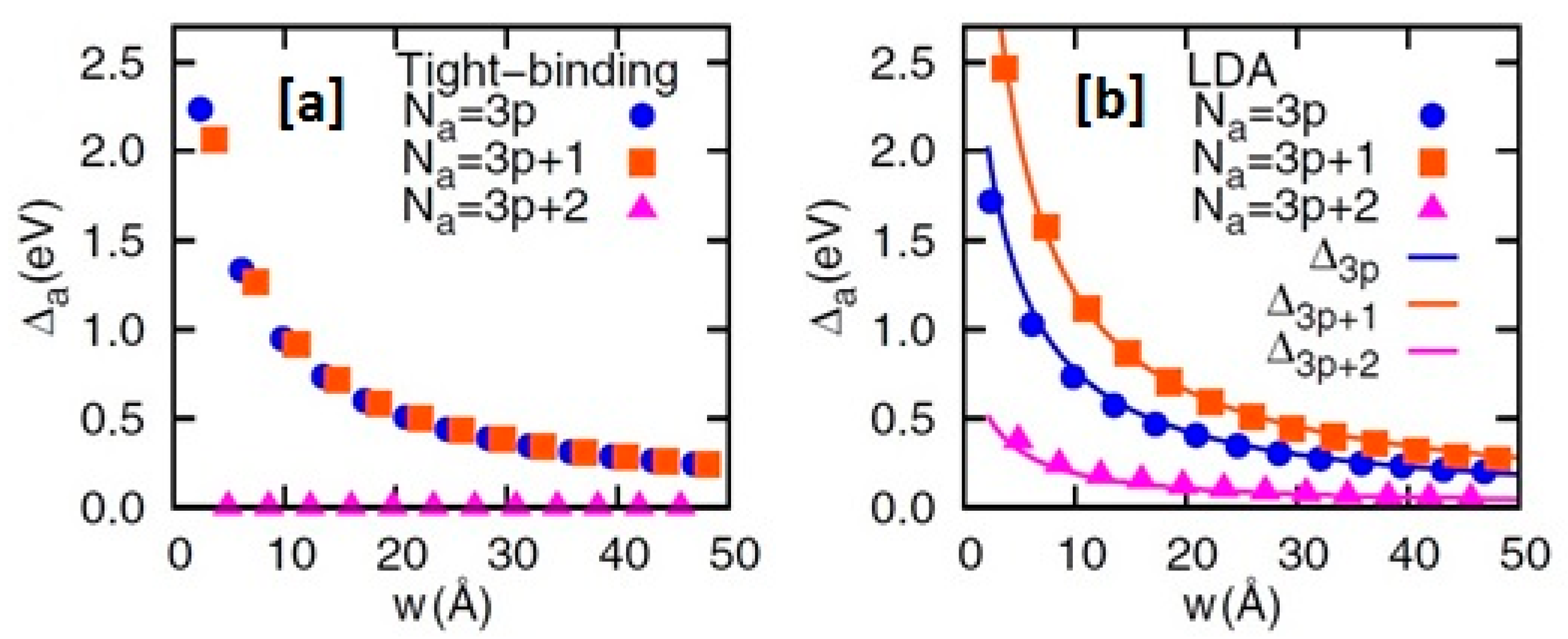
The overall calculations report that the energy gap of the armchair GNR decreases with the increase of the nanoribbon width (w) [5,39]. The energy gap obtained from the tight binding (TB) model is significantly different from the first-principles calculations. The TB model results using nearest neighbor hopping integral, t = 2.7 eV [41], between π-electrons, are represented as a function of the width in Figure 4a for N = 3p, 3p + 1, and 3p + 2. Similar results are also calculated by the first-principle study and are presented in Figure 4b. In Figure 4a, the TB model results clearly reveal that the armchair GNR is semiconducting in nature, except for N = 3p + 2. The energy gap of the armchair GNR (Δa) is inversely proportional to its width and increases with the hierarchy of Δ3p ≥ Δ3p+1 > Δ3p+2 (=0) for any value of p. The non-metallic nanoribbons are shown in the first-principle calculation and the hierarchy of energy gap maintains Δ3p+1 ≥ Δ3p > Δ3p+2 (≠0), as shown in Figure 4b [39].
3. Synthesis and Fabrication Techniques of GNR Interconnects
The atomic structures and geometric properties of the graphene nanoribbon (GNR) interconnect strongly depend on its synthesis techniques. Depending on the pattern and structure, metallic or semiconducting GNR interconnects are produced [8,42].
Various fabrication methods are proposed for graphene synthesis for the interconnect applications, and difficulties exist in every method. The developed graphene films are not purely single crystal, which can provide extraordinary electrical conductivity. Only a few layer graphene are suitable for the interconnects application, but the uncontrolled fabrication produces multilayer graphene that turns to graphite, which has a much lower conductivity because of the interlayer electron hopping [43]. Graphene can be synthesized by mechanical exfoliation from graphite and deposited onto an insulating substrate [44], but this technique is also uncontrollable and hence it is not suitable for mass fabrication. The epitaxial growth of graphene on SiC substrates is a potential method for wafer-level graphene synthesis. However, this method will not be suitable for interconnect fabrication, because the graphene nanoribbons are to be deposited on dielectric substrate for on-chip interconnects applications [5,8]. The synthesis of graphene by the segregation method, using a Ni or Cu substrate, followed by the transfer to another insulating substrate for pattering, is the most popular and suitable approach for interconnect applications [8,32].
Graphene nanoribbon fabrication techniques are basically three types, for example, (i) the cutting of graphene film along an appropriate direction using lithography, (ii) bottom-up synthesis from precursor molecules, and (iii) unzipping of carbon nanotubes (CNTs) [45].
For interconnect applications, GNRs are synthesized by shaping the graphene film only where chemical vapor deposition (CVD) is the common technique used to synthesize single or multilayer graphene film [21,28,30,46,47,48,49,50,51]. CVD-grown graphene films are large area polycrystalline in nature, where the grain sizes vary from tens of nanometers to micrometers [48]. Recently, CVD-grown graphene has been investigated as a promising material for micron level interconnects for complementary metal oxide semiconductor (CMOS) devices [52], and as interconnect materials in stretchable Si devices [53]. But, theoretically, the studied GNR interconnects are in few nanometer scales and could be smaller than the crystallite size of the CVD-grown graphene [47].
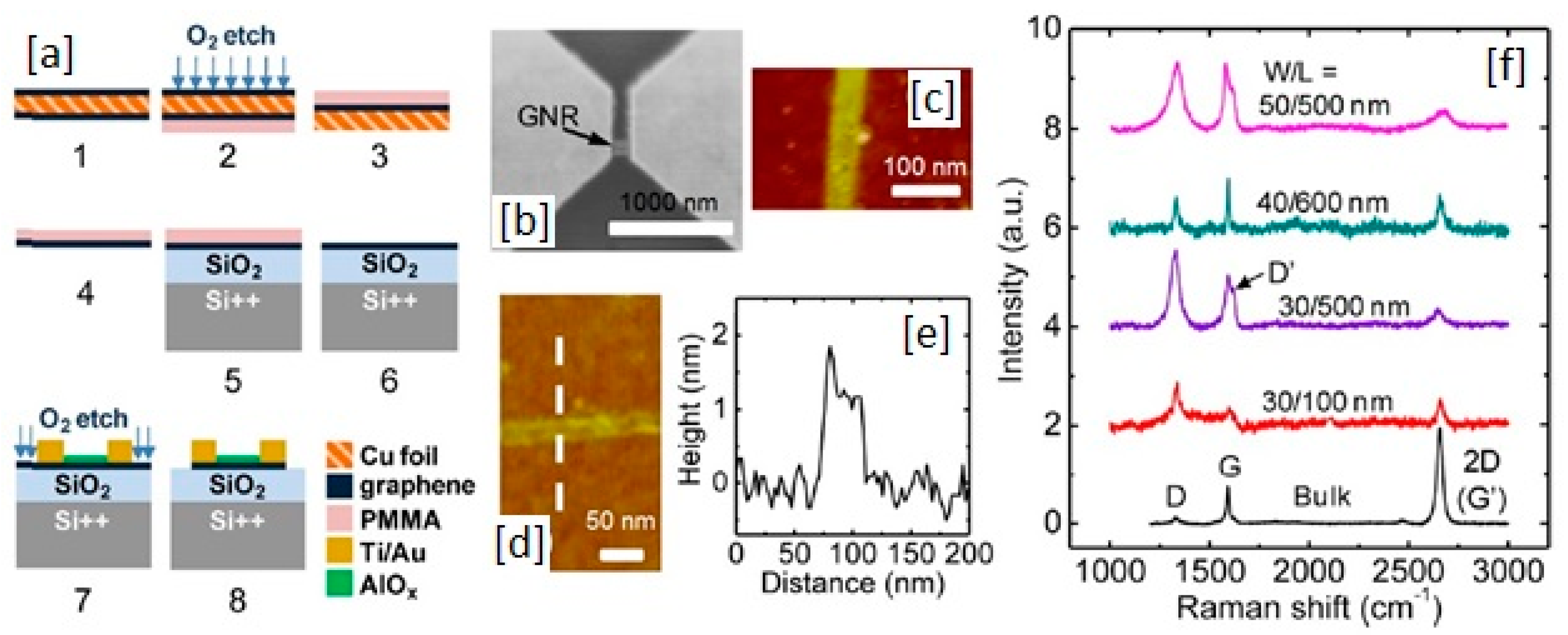
Behnam et al. [47] fabricated graphene nanoribbons with different widths (w) (e.g., 75, 60, and 53 nm) by using the standard CVD technique, as summarized in Figure 5a. The GNRs were placed on a N–Si substrate between two Au/Ti contact electrodes, as shown in the SEM image in Figure 5b. The AlOx layer was used to protect the GNR film, and AFM images were captured showing the width and thickness of GNRs (Figure 5c–e). The CVD-grown bulk graphene and GNRs with different aspect ratio were characterized by Raman spectroscopy (Figure 5f). The CVD graphene showed a narrow 2D peak, where a defect induced D′ peak was invisible. The D band intensity increases because of an increase of fraction of edge carbons. A significant disorder in D and D′ was observed in Figure 5f, in the case of graphene nanoribbons of different aspect ratio due presence of edges [47,54,55].
The CVD-grown graphene layers are transferred to the doped Si substrate, and the GNRs interconnects are patterned using photolithography and are given shape by the oxygen plasma etch, as reported [21,30,46].
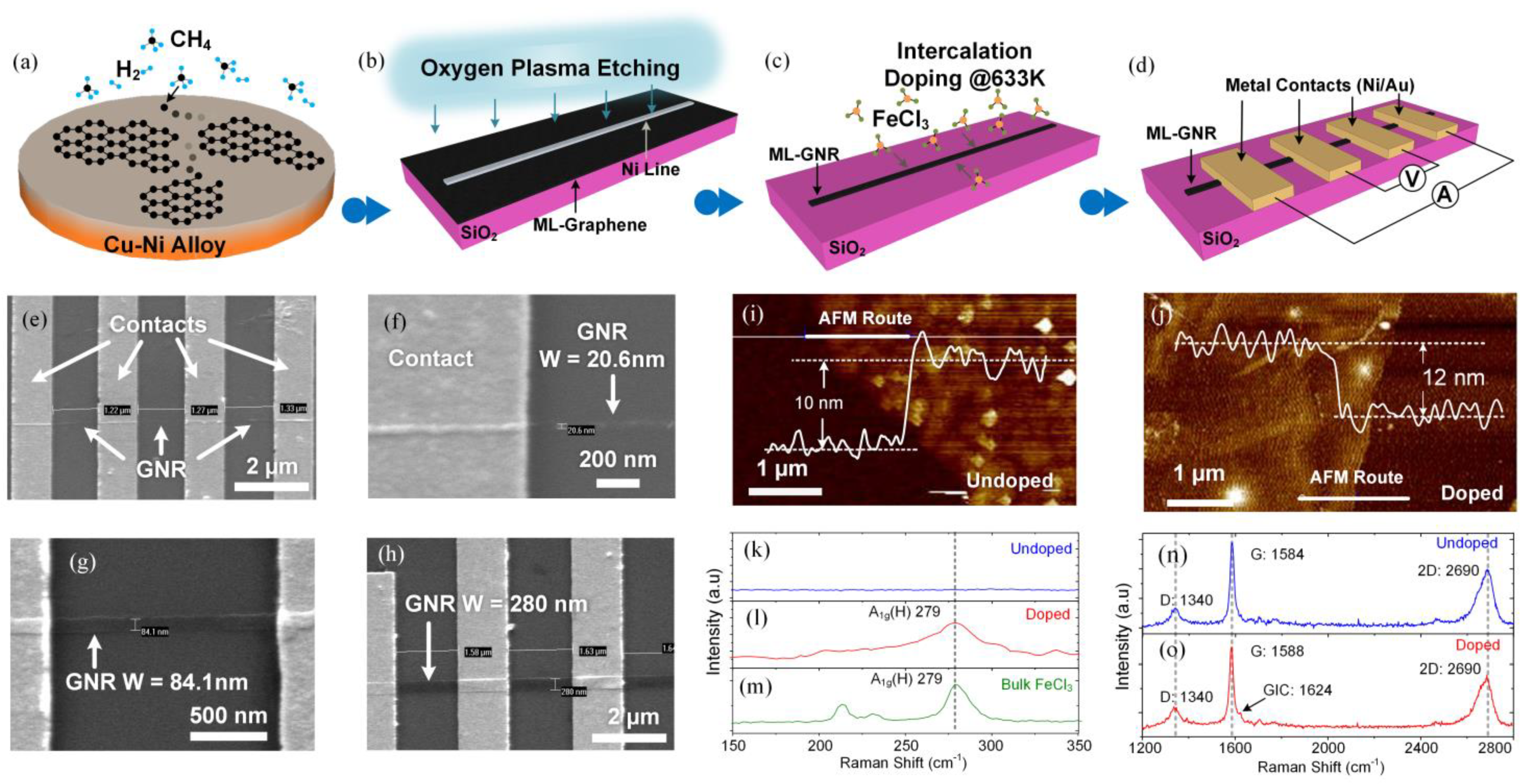
The CVD-grown and intercalation-doped multilayer-graphene-nanoribbons (MLGNRs) were reported by Jiang et al. [28] for their superior interconnect application. A Cu–Ni catalyst was used for 10–15 layers of ML-graphene synthesis, where the number of the layer was controlled by changing the ratio of Cu and Ni. After transferring the MLGNR layer to the Si substrate, the Ni/Au alloy contacts were made for resistivity measurement (Figure 6d). MLGNR with different widths (e.g., 20.6, 84.1, and 280 nm) were grown and are shown as SEM images (Figure 6e–h). FeCl3 intercalation doping was done to enhance the electrical conductivity of MLGNR. The doping was carried out at 633 K and ~1.4 atm pressure for 10 h in an Argon atmosphere. Because of intercalation doping, the MLGNR thickness was increased from 10 to 12 nm, which is clearly shown in Figure 6i,j [28].
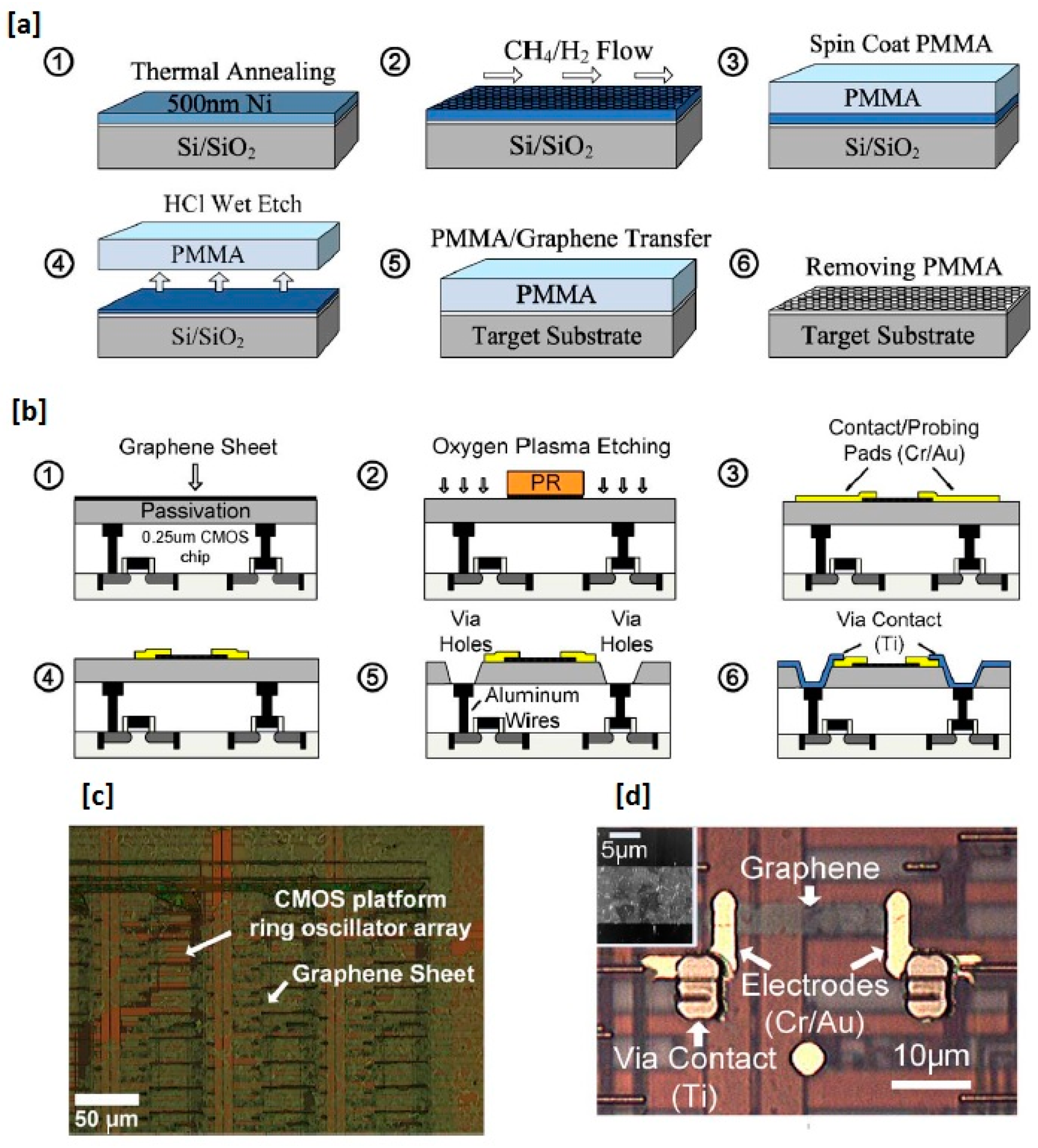
Chen et al. [52] reported the fabrication of graphene interconnects and application in CMOS integration, as shown in Figure 7. An approximately 15–20 nm thick multilayer graphene was synthesized using the standard CVD method on the Si/SiO2 substrate. The graphene layer was transferred to the target substrate through the poly methyl methacrylate (PMMA) assisted method, clearly shown in the process flow chart of Figure 7a. Then, the standard CMOS-compatible fabrication technique was adopted, where the graphene interconnects were patterned into stripes of different widths/lengths by optical lithography and oxygen plasma etching. The graphene interconnects were shaped with a 3–5 µm width and 5–145 µm length. The Cr/Au contact was taken from the graphene interconnects. The via connections were taken from the top most metal layer of metal-oxide-semiconductor (MOS) through the passivation layer, shown in Figure 7b. The via contacts were made from Ti metal. Clear optical images were captured showing graphene interconnects on the top layer of the ring oscillator array circuit in CMOS process (Figure 7c,d).
The patterning of graphene by the conventional photolithography technique offers rough edges in the GNR interconnects, and the MFP of GNR reduces significantly as a result of edge scattering. A potential chemical technique was proposed by Ci et al. [56] for the controlled nano-cutting of GNR along the crystallographic direction, producing smooth edges with an armchair or zigzag structure. A uniform Ni nanoparticles film was deposited on highly-ordered pyrolytic graphite (HOPG) plates. After drying, HOPG was annealed at 500 °C in Ar mixed with 15 vol% H2 for 1 h, resulting in the formation of Ni nanoparticles on their surfaces. Ni nanoparticles can act as knives to pattern graphene and the size of the Ni nanoparticles controls the edge of ribbons (armchair and zigzag) [5,56].
4. Basic Circuit Model of GNR Interconnects
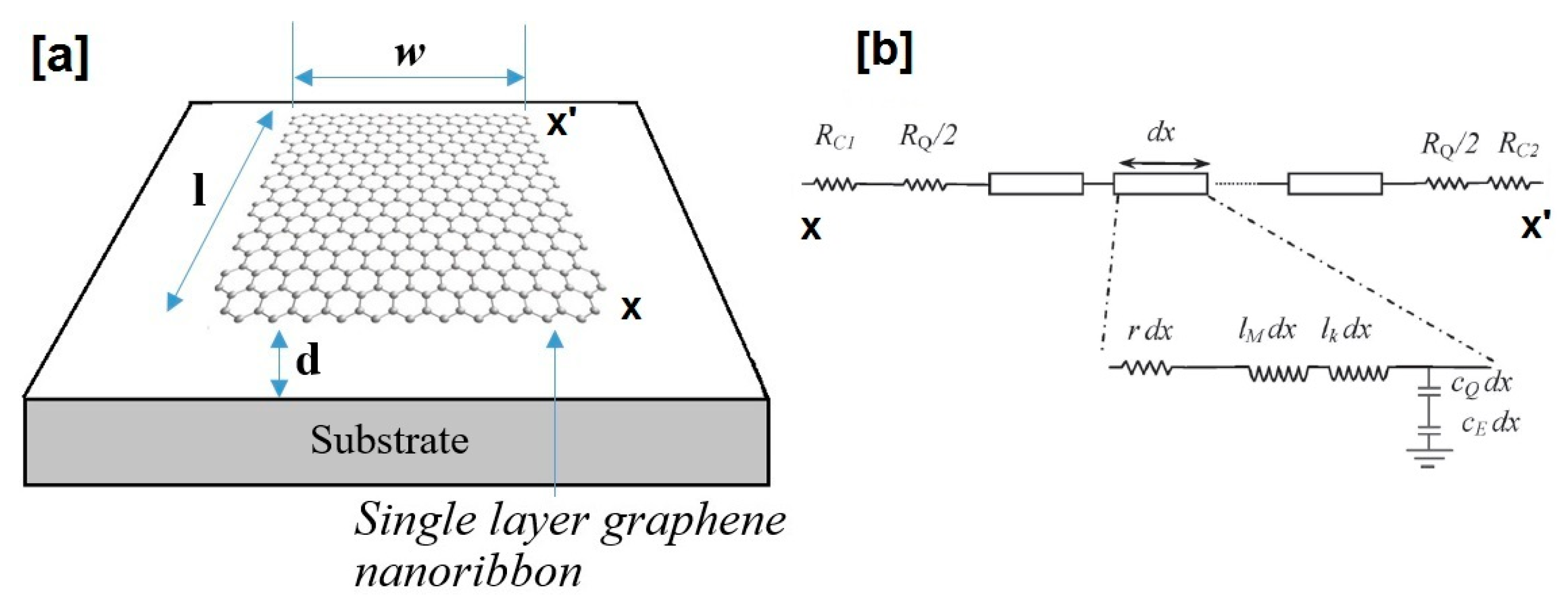
The structure of a single layer graphene interconnect has been illustrated in Figure 8a, where x and x′ are the contact ends. In Figure 8a, l and w are the length and width of single layer GNR, respectively, and d is the displacement of GNR from the substrate. Figure 8b shows a schematic representation of a typical RLC model for a single layer GNR interconnect. At both ends of the circuit model (i.e., x and x′), RC1 and RC2 are the contact resistances and the values depend on the quality of the contacts [5]. The values of contact resistances for single and few layer graphene nanoribbons are as small as small as one hundred ohms, as reported by Han et al. [57]. RQ is the quantum resistance of an ideal quantum wire, assuming zero scatterings at the contacts and throughout its length, as represented in Equation (1) [5,58].
where h is Planck’s constant, e is the electron charge, and Nch is the number of conduction channels (modes) in one layer [8].
In Figure 8b, dx is the differential element along the length of GNR interconnects where CE and lM represent electrostatic capacitance and magnetic inductance per unit length and are considered in the model like any other conductor. Values of CE and lM are determined by the geometry and the materials surrounding them and are represented by Equations (2) and (3).
where, ε and µ are the dielectric permittivity and permeability of graphene, respectively. CQ and lK are the quantum capacitance and kinetic inductance per unit length. CQ and lK are not mutual components, and their values may increase and decrease linearly with increase of the number of the conduction channel (Nch). CQ and lK are modeled in Equations (4) and (5), as follows [5,59,60].
where vF (8 × 10⁵ m/s) is the Fermi velocity in graphite [59,60]. The mean free path (MFP) of GNR is very long but finite. The electrons in GNR can get scattered by phonons, defects, and rough edges. So, the resistance per unit length of a GNR can be modeled by Equation (6) [18,59].
where λeff is the effective MFP. The number of conducting channels (Nch) in each GNR can be calculated by considering the contributions of all of the electrons in all of the NC conduction sub bands and all of the holes in all of the NV valence sub bands, as represented in Equation (7) [8,59,61,62].
where i, EF, k, and T are the positive integer, Fermi energy, the Boltzmann constant, and temperature, respectively. Ein and Eih are the minimum energy of electron and hole in the ith conduction sub-band, as represented in Equation (8) [5,35,63].
ΔE is the sub-band energy in metallic GNR and β is zero for the metallic GNR, and 1/3 in the semiconducting GNR. This quantization is taken into consideration because of the limited width of the graphene nanoribbon [59,63].
The number of conduction channels, that is, Nch = G/G0 (G0 = 2·e2/h) in metallic and semiconducting graphene nanoribbons, are obtained using the non-equilibrium green function (NEGF), and are plotted as a function of the GNR width (w) in Figure 9a,b, respectively, where the Fermi energy was considered between 0 to 0.3 eV. Figure 9b shows no conduction channels in the narrow semiconducting armchair GNRs [5].
5. Circuit Model of Multilayer GNR Interconnects
The electrical resistance of a single layer graphene nanoribbon (GNR) is relatively high compared to Cu. A multilayer GNR (MLGNR) with a reduced equivalent resistance is more suitable for interconnect applications [8,21,46,64]. Also, the resistance of the MLGNR interconnects scales inversely with the number of layers [7]. The multilayer of graphene with van der Waals bonding is patterned into a few tens-of-nanometers-wide ribbons, and it offers a promising solution to the interconnect scaling issues [28,65].
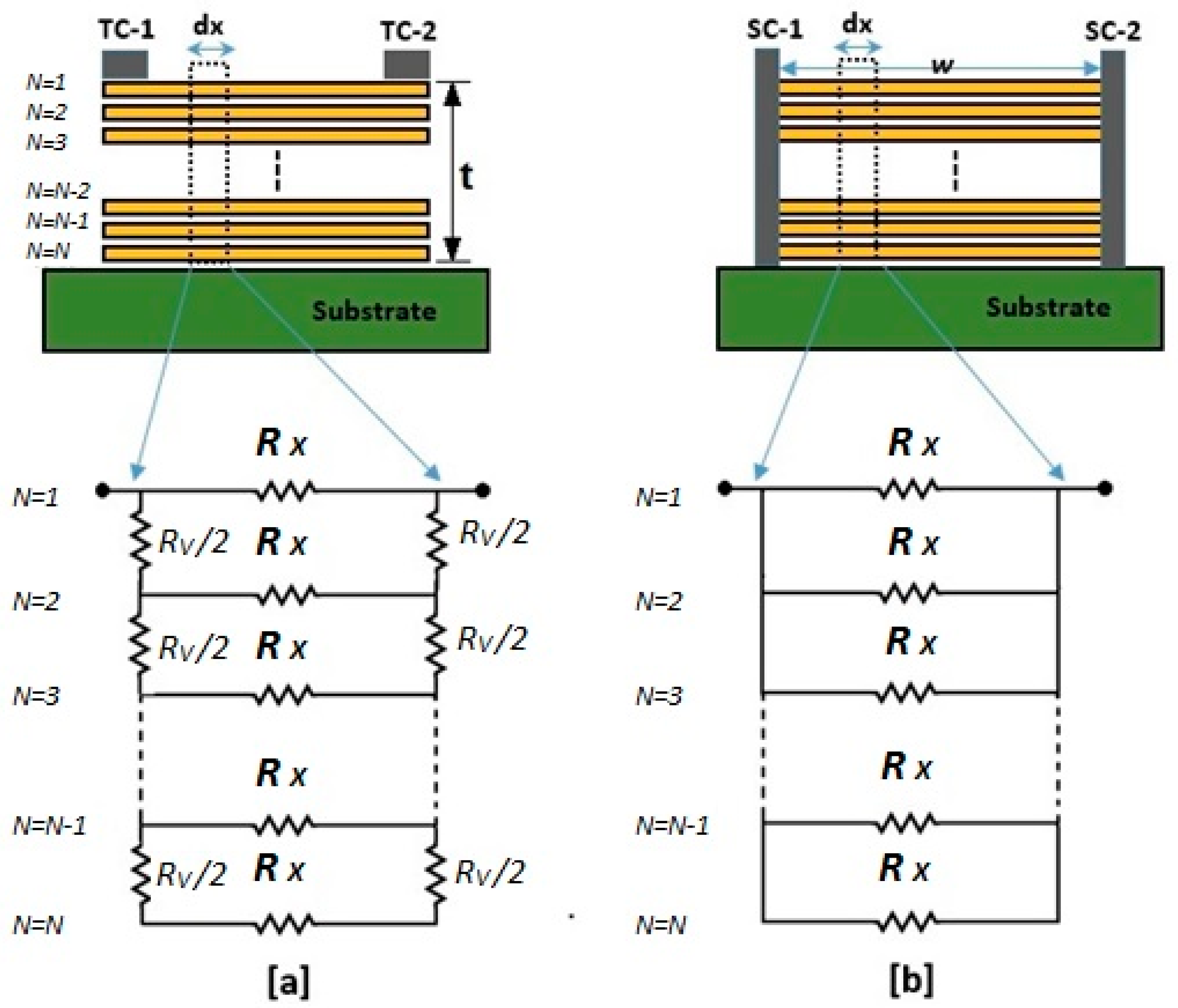
From the circuit analysis point of view, two types of contact technology are preferred, that is, (i) top contact (TC) technology, where metal contacts are taken from the top surface of MLGNR, as shown in Figure 10a, and (ii) side contact (SC) technology, where the metal contacts are taken from two sides of the GNR stack, as shown in Figure 10b. In TC technology, contact formation is very easy, but the effective resistance is high because the GNR layers are not in the parallel combination. On the other hand, the effective resistance is very low with SC technology, because of the parallel connections of the GNR layers between two contacts, as shown in Figure 10b. Of course, the fabrication is difficult with SC technology [7,66].
The interlayer spacing (δ) between the parallel layers is approximately 0.35 nm and total number (NLayer) of single layer graphene nanoribbons (SLGNR) can be expressed, as in Equation (9) [7].
The equivalent resistive circuit model of the MLGNR interconnects for TC and SC technology have been represented in Figure 7a,b, respectively, considering the c-axis resistivity of graphene. Rx, in Figure 10, is modeled in Equation (10), by using Equations (1) and (6).
The effective mean free path (λeff) of MLGNR, expressed in Equation (11), depends on the defects-induced MFP (λd) and MFP (λEdge), due to diffusive scattering near the GNR edges [7,67].
The defects-induced MFP (λd) significantly depends on the type of substrate and can be obtained up to ~1000 nm for the suspended GNR. The MFP of graphene on the SiO2 substrate is roughly 100 nm, because of charge impurity and phonon scattering [7,67]. A recent study confirms that MFP increases up to 300 nm for a hexagonal boron nitride substrate, which can be considered as the realistic defects-induced MFP (λd) for MLGNR interconnects [68,69]. The MFP due to the edge scattering (λEdge) of GNR can be expressed in Equation (12).
where w is the width of the GNR, p is the backscattering probability of the electron near the GNR edges, p = 0.2 is the realistic value, and p = 0 signifies the smooth edges. EF and ΔE are the Fermi energy and sub band energy of metallic GNR, respectively, i is the number of sub band, and β is zero for the metallic GNR and one third for semiconducting GNR [7,63]. The interlayer resistance per unit length (RV) for MLGNR is represented in Equation (13) [7].
where ρc is the c-axis resistivity of graphene and δ is the interlayer spacing (~0.35 nm). The c-axis resistivity was measured as 0.3 Ωm for highly oriented pyrolytic graphite (HOPG) [70]. The equivalent resistance per unit length (RN) for the N-layer GNR with a top contact (TC) structure is presented in Equation (14) (Figure 10a) [66].
The equivalent resistance per unit length (RN) for the N-layer GNR with a side contact (SC) structure is presented in Equation (15) (Figure 10b) [66].
So, the net resistance of the N-layer SC-MLGNR interconnect is given as in Equation (16),
and the net resistance of N-layer TC-MLGNR interconnect is given in Equation (17), as follows:
The quantum capacitance (CQ) and kinetic inductance (lk) of the multilayer GNR are increased and decreased, respectively, with the increase in the number of layers in MLGNR, as shown in Equations (18) and (19).
6. Performance of GNR Interconnects and Comparison with Other Materials
In the previous sections, the structural properties, fabrication process, and basics of circuit modeling of single and multilayer graphene nanoribbon interconnects were highlighted. Also, the different electrical quantities of the graphene nanoribbon were elaborated on, in order to rely on its potentiality as on-chip interconnects. In this section, the performance of the GNR interconnects in terms of resistivity, capacitance, propagation delay, crosstalk effect, and stability are compared with the existing cutting-edge interconnect material, like copper. Also, the performance is compared between the carbon nanotubes (CNTs), single layer GNR, multilayer GNR, and doped GNR as the future promising interconnect materials.
6.1. Resistivity
In recent years, resistivity problem has become more serious in the existing interconnect materials, like Cu and W, because of the high integration in ICs. As the interconnect width decreases, the resistivity of the Cu interconnects increases tremendously, because of the grain boundary and side wall scattering of electrons [10,71]. The CNTs and graphene attract attention because of their large mean free path (ideal MFP ≈ 1 µm) and very high carrier mobility [33]. Because of edge scattering, the effective MFP decreases significantly in GNR, compared to CNT. Also, the mobility in GNR decreases with the lowering width (below 60 nm) [10,72]. The metallic and semiconducting properties of GNR depend on its chirality [19,73,74]. But a high quality graphene strip and single wall carbon nanotube (SWCNT) can conduct with a large current density and an almost similar magnitude [75]. However, the major advantages of GNR over SWCNT are its straightforward fabrication, well defined chirality compared to random chirality of CNTs, proper control of its band gap, MFP, mobility, and resistivity [33].
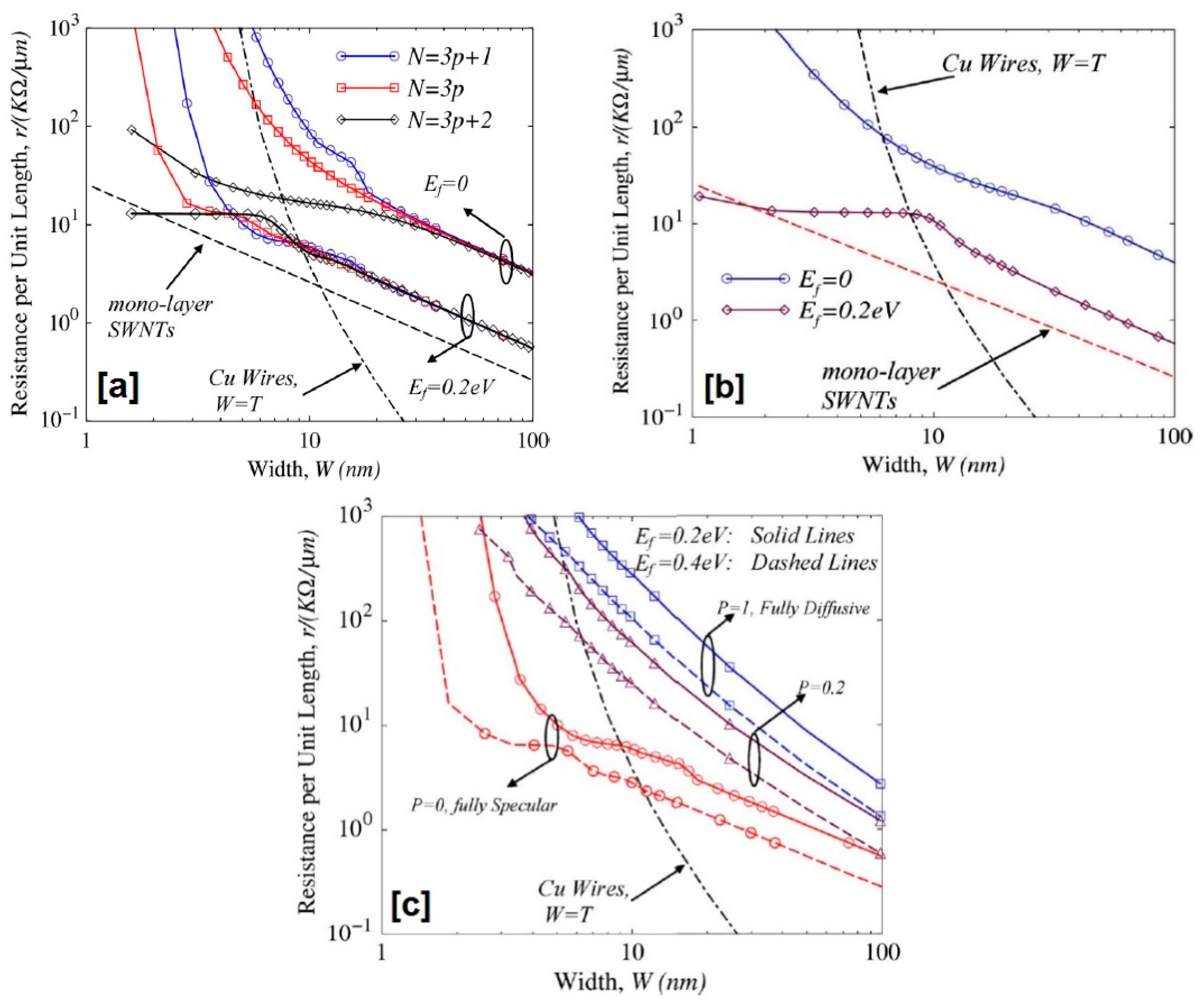
However, in a performance comparison, (i) the theoretically calculated global resistances or resistance per unit length (Ω/µm) and (ii) practically measured resistivity (µΩcm) of different interconnects are described as the function of width (w in nm). Naeemi et al., [33] in their physical model, showed the per unit length resistance values (Ω/µm) of the metallic and semiconducting GNRs, monolayer SWCNT, and copper wire interconnects as the function of width (w), where they considered the length to be larger than the MFP (Figure 11), where the thickness of the copper wire was assumed to be 7% of its width for w > 30 nm and 2 nm for w < 30 nm. From the same figure (Figure 11), we also observe that for w > 100 nm, both the metallic and semiconducting GNRs have similar trends of resistance. Below a 100 nm semiconducting, GNRs have a very high resistance, and below a 5 nm width, they become virtually insulators. For metallic ribbons, the resistance is constant below 20 nm, because of the diffusive edge scatterings resulting in short MFPs. For w ≤ 8 nm, the models reveal that metallic GNRs offer a lower resistance than copper wires with the unity aspect ratio. However, the SWCNT interconnects offer smaller resistances compared to all types of GNRs and for all widths [33].
The resistance per unit length (Ω/µm) of the GNR interconnects was theoretically calculated and plotted as a function of the width (w), as shown in Figure 12 [5]. Considering the smooth edge approximation (MFP ≈ 1 µm) in the TB method, the resistance was calculated for single layer armchair and zigzag GNR in Figure 12a,b, respectively, and compared with the Cu wires (unity aspect ratio) and SWCNT with a random chirality. In Figure 12a, the semiconducting (N = 3p + 1 and N = 3p) and metallic (N = 3p + 2) type armchair GNR, and in Figure 12b, the zigzag GNR for the Fermi energy (Ef) of 0 and 0.2 eV were compared with Cu and SWCNT. The single layer GNRs have a resistance per unit length smaller than Cu for a width below 8 nm [5]. The per unit length resistances of single layer GNRs are plotted versus width, in Figure 12c, considering the edge backscattering probability P = 0, 0.2, and 1, and Fermi energy of 0.2 and 0.4 eV. It is clearly evident from Figure 12c that the edge roughness can increase the resistances of the GNR interconnects by an order of magnitude, especially for the small widths. So, a proper patterning method for getting smooth edge GNRs is essential for practical application. Additionally, an increase of the Fermi level in GNR lowers their per unit length resistances considerably [5].
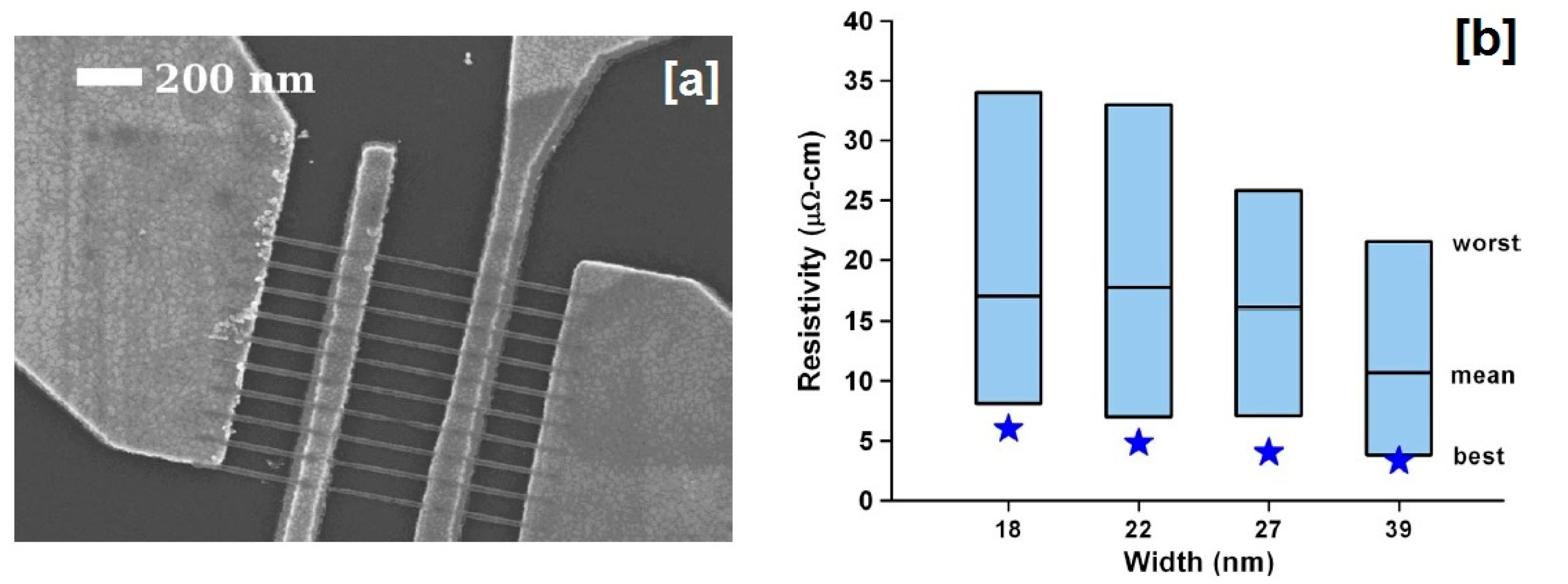
So, the theoretical results as discussed above confirm that the resistance per unit length is lowered in case of single layer GNR, only below 8 nm of width. Therefore, the overall superior conductivity is offered by a single wall carbon nanotube (SWCNT) compared to GNR and Cu. The 2D resistivity of the GNRs were measured and compared with that of Cu by Murali el al. [9]. The graphene flake was collected from the graphite piece and patterned in graphene nanoribbons by photolithography technique with dimensions of 18 nm < w < 52 nm and 0.2 μm < L < 1 μm. The Au/Ti contacts were taken from the GNR surface, as shown in the SEM image in Figure 13a. To mask the non-uniformity of the width of the different GNRs, ten GNRs were measured in parallel configuration and calculated for single GNR. The GNR showed 2–3 times less resistivity (µΩcm) than Cu at T = 300 K within the range of 18 nm < w < 52 nm. It was collected from International Technology Roadmap for Semiconductors (ITRS) 2007 data. The resistivity of the individual GNR was extracted from sets of parallel GNRs and was plotted in Figure 13b. It was found that the best resistivity of GNR for a given width was comparable to a Cu wire of same width. Because of the different scattering mechanism of GNRs on a SiO2 substrate, the mobility was reduced, thereby limiting the measured resistivity of GNRs.
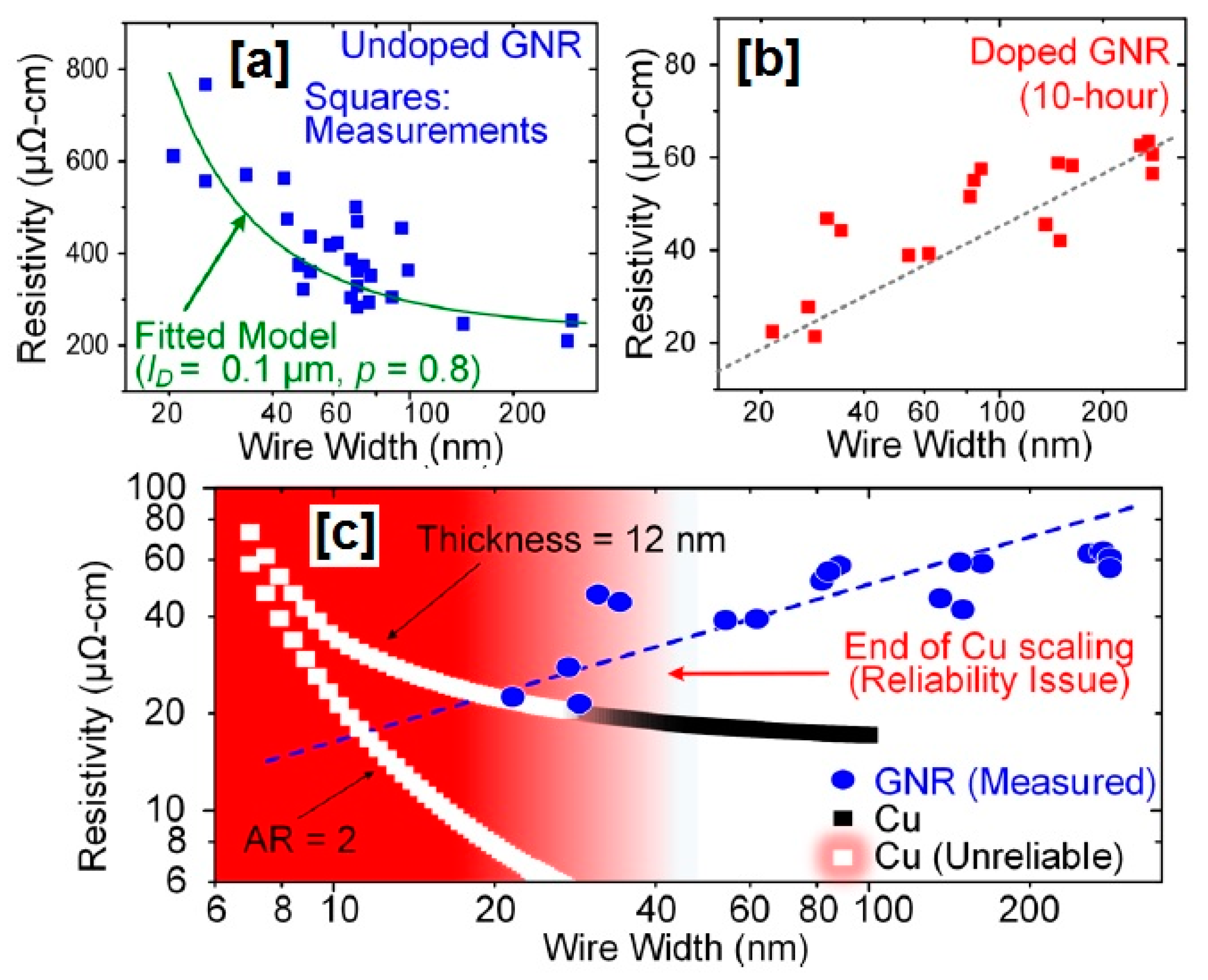
The resistivity of the undoped and FeCl3 intercalation doped MLGNRs were practically measured by Jiang et al. [28], and compared with the resistivity of Cu. The multilayer graphene was synthesized using the CVD method, and the MLGNRs were patterned using the photolithography method. A detailed fabrication process has been discussed in Section 3. Figure 14a,b represent the measured resistivity of the undoped and doped MLGNR for a width of 20 nm < w < 200 nm. The measured resistivity of the undoped MLGNRs are significantly high compared to the doped one, and interestingly, the resistivity is decreased at the lower width of the doped MLGNRs (Figure 14). However, the resistivity of the doped MLGNRs and Cu was compared as a function of the width (w) in Figure 14c, where a 12 nm thickness was considered for both. The Cu interconnects suffer from a reliability issue below a 40 nm width, because of the grain boundary and side wall scattering [10,71]. At a 20 nm wire width (Figure 14c), an almost similar resistivity is observed for the doped MLGNRs and Cu interconnects when both are 12 nm thick. The Cu wire with an aspect ratio two offers a much lower resistivity compared to the doped MLGNR at w = 20 nm, but Cu suffers from a reliability issue (Figure 14c) [28].
The resistances of Cu, SWCNT bundles, mono-layer zigzag (zz) GNR, multi-layer (ML) zz-GNR, tungsten (W), and AsF5 doped ML-zz-GNR were measured in the form of both global and local interconnects, in Figure 15a,b, respectively [8]. For the local interconnects, the individual length is given in Figure 15. Below a 22 nm technology node, the SWCNT bundles are the best, while all of the GNR structures have a higher resistivity than Cu for both the global and local wires. However, the AsF5-doped multilayer GNR always performs better than the undoped mono and multilayer zz-GNRs.
6.2. Capacitance
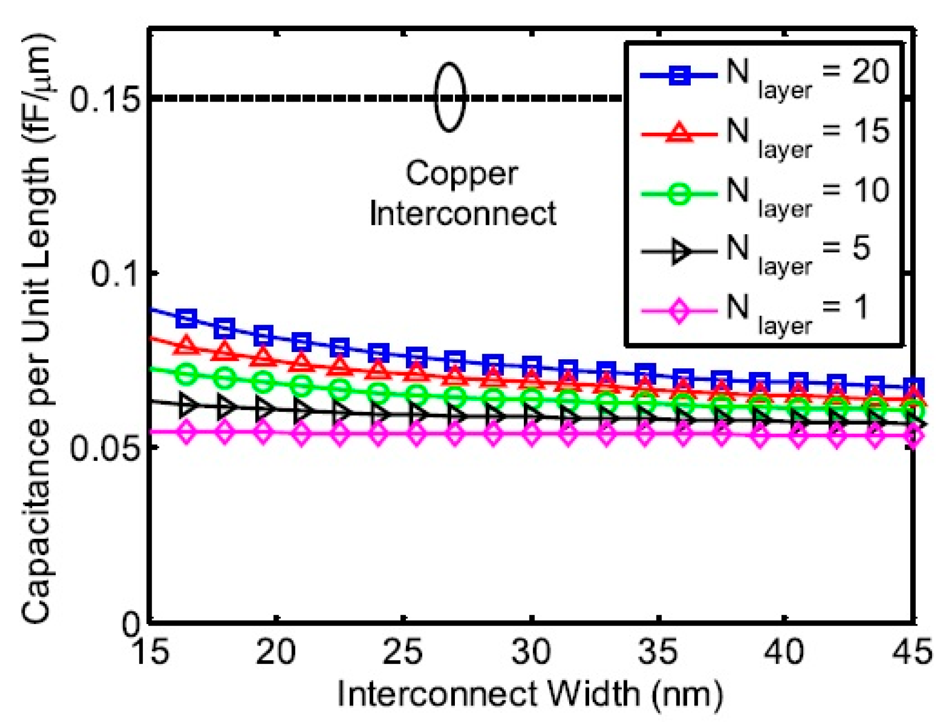
The potentiality of the interconnect materials strongly depends on its intrinsic and parasitic resistance and capacitance. The resistance and resistivity of the graphene nanoribbon interconnects have been discussed elaborately in previous sub-section, and an overall higher value was found compared to the Cu interconnects. But, the estimated capacitance per unit length (fF/µm) for the GNR interconnects shows a lower value compared to the Cu interconnects, because of the extremely lower thickness of the graphene film. Obviously, the capacitance increases with the increasing number of graphene layers.
The capacitance value of the GNR interconnects is estimated by considering the quantum capacitance and electrostatic capacitance, and is simulated by the Raphael simulation reported by Pan et al. [76]. The capacitance of GNR interconnects with the variable layers (from 1 to 20) are compared with the Cu interconnects for a variable width of 15 nm < w < 45 nm, as shown in Figure 16. Although, the capacitance per unit length is increased with the number of graphene layers (from 1 to 20), and the overall value of the capacitance is significantly less compared to the Cu interconnects.
6.3. Delay and EDP
After the individual comparison of the resistance and capacitance of the graphene nanoribbon interconnects with the Cu interconnects, as discussed in the previous section, the propagation delay and energy delay product (EDP) of MLGNR is compared with the Cu interconnects [3,7] in this section.
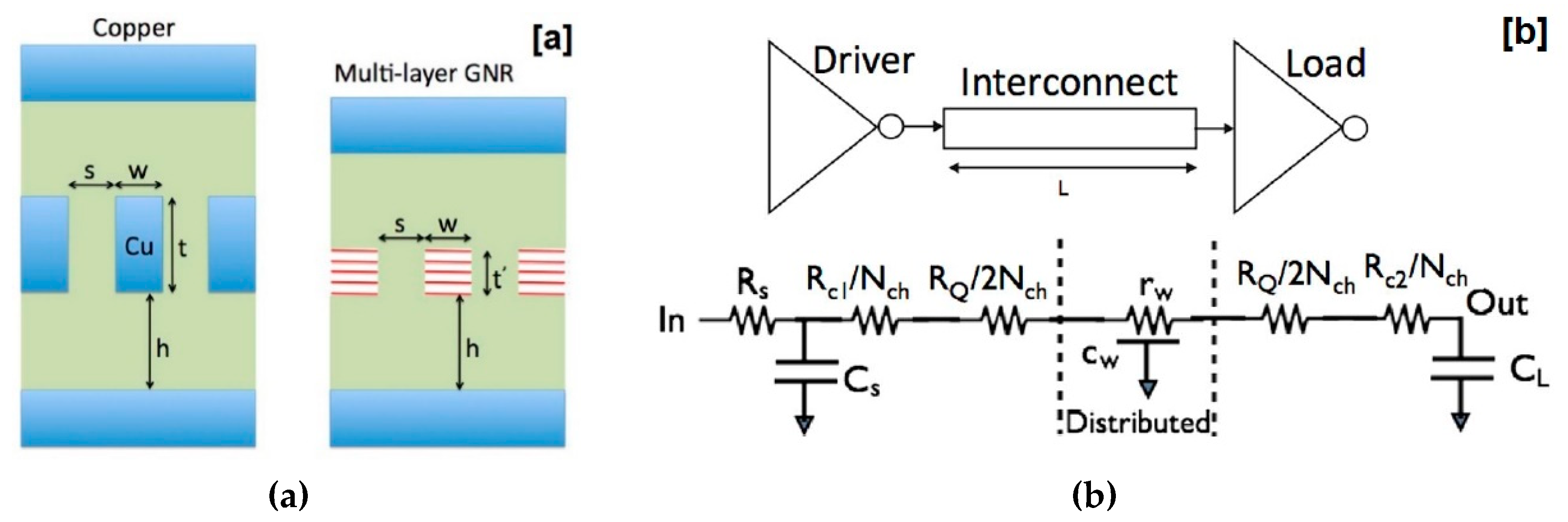
The cross sections of the Cu and MLGNR interconnect are shown in Figure 17a, and the schematic of the circuit delay is shown in Figure 17b. The 50% system delay expressions for the MLGNR interconnects (td_MLGNR) and for the Cu interconnects (td_Cu) from Figure 17b are represented by Equations (20) and (21), respectively [7]. Coefficients 0.69 and 0.38 were used to represent the propagation delay of the lumped and distributed network, respectively.
The distributed capacitance, CW, is the series combination of the electrostatic capacitance and the quantum capacitance. The energy dissipation of the same system (Figure 17b) is presented in Equation (22).
where VDD represents the bias voltage.
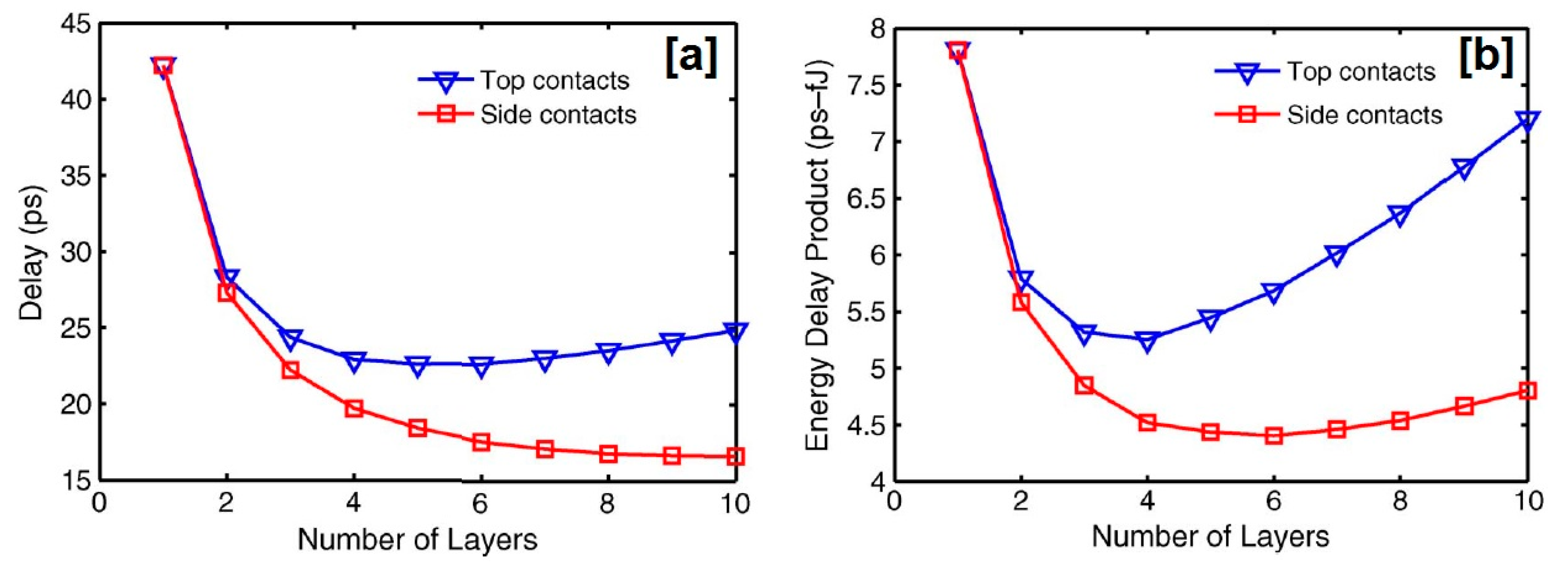
If the number of layers in MLGNR increases, the effective resistance for both the top contact (TC) and side contact (SD) devices will decrease. At the same time, the equivalent capacitance will increase with the increasing number of layers in MLGNR. So, an optimal point is expected, where a 50% RC delay and EDP will be minimum for a particular number of layers in the MLGNR interconnect. The delay versus number of layers, and EDP versus number of layers, as plotted in Figure 18a,b, exhibit a minimum point in the cases of both the TC and SC-MLGNR interconnects. The minimum delay and EDP are obtained in the case of SC compared to TC. So, TC-MLGNR requires a fewer number of layers compared to SC-MLGNRs, in order to minimize the delay and EDP. It signifies that the interconnect capacitance has a stronger impact on the top contact compared to the side contact of the MLGNR.
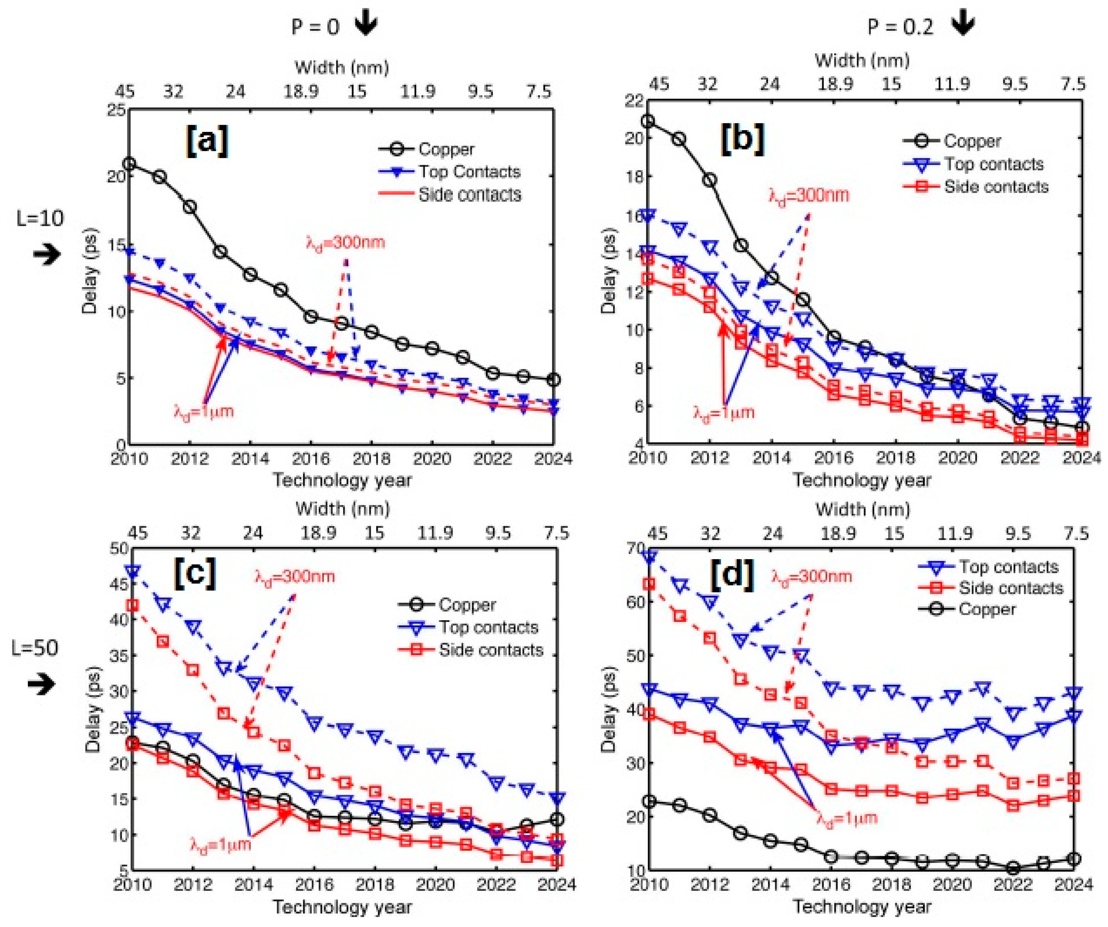
Figure 19 shows the delay as a function of the MLGNR and Cu interconnects width, correlated with the ITRS technology year. A delay is represented for the GNR edge backscattering probability of 0% (P = 0) and 20% (P = 0.2). Also, two different cases are considered for the (i) minimum-sized driver (W/L = 1) with l = 10 gate pitches and (ii) five-times of the minimum-sized driver (W/L = 5) with l = 50 gate pitches.
For the minimum-sized driver, a smooth edge (P = 0) MLGNR performs better for all of the width and MFP of 1 µm and 300 nm, compared to the Cu interconnects (Figure 19a). For the 20% edge scattering, the Cu interconnects perform better than the TC-MLGNR below a 15 nm width (Figure 19b). For a five-times minimum-sized driver, the SC-MLGNR with a MFP of 1 µm performs better than the Cu interconnects for all of the technological nodes (Figure 19c). But, the Cu interconnects perform better than all of the MLGNR for P = 0.2 (Figure 19d).
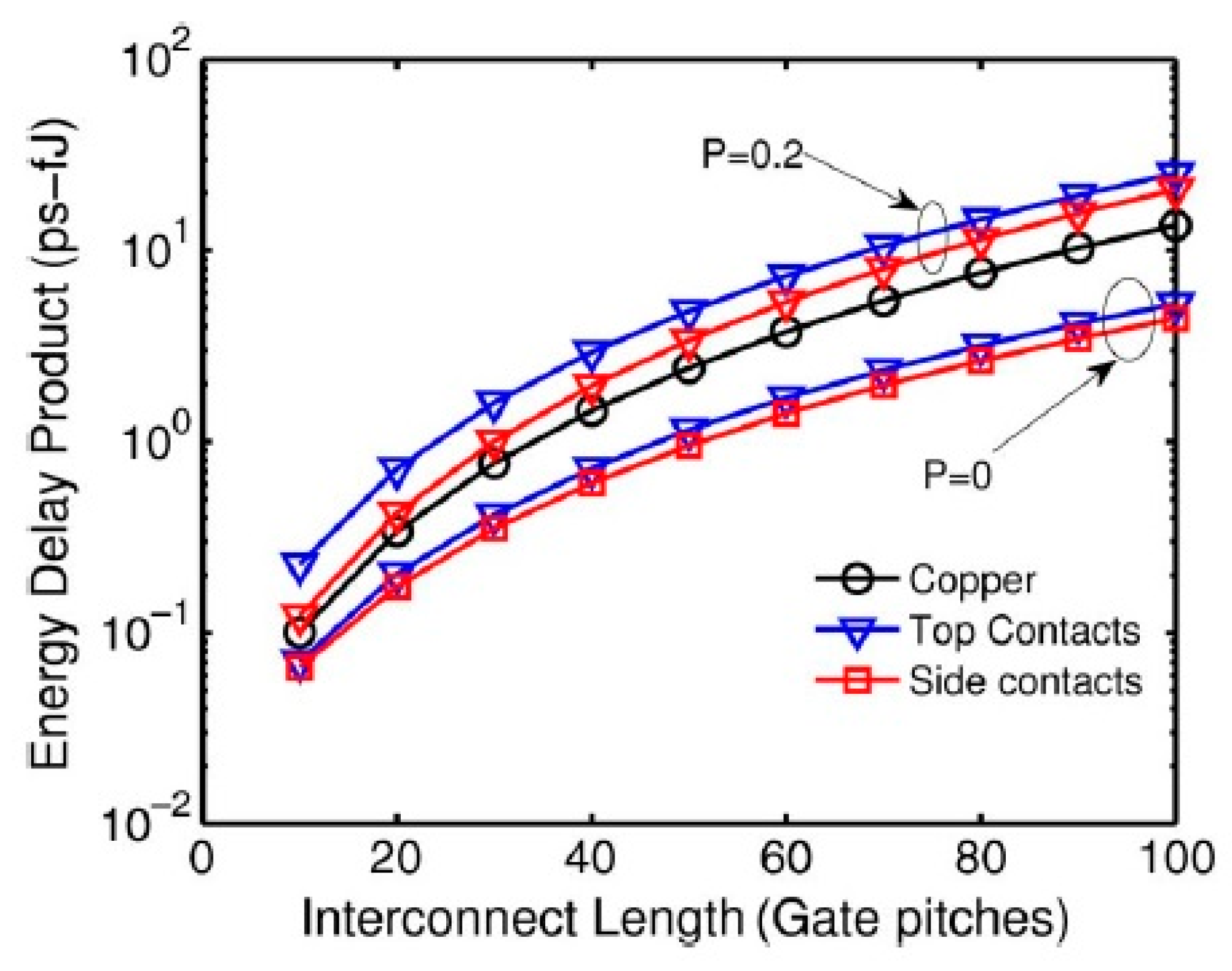
The EDP performance is better for a smooth edge (P = 0) MLGNR in a 9.5 technology node for any interconnect length, compared to the Cu interconnects, shown in Figure 20.
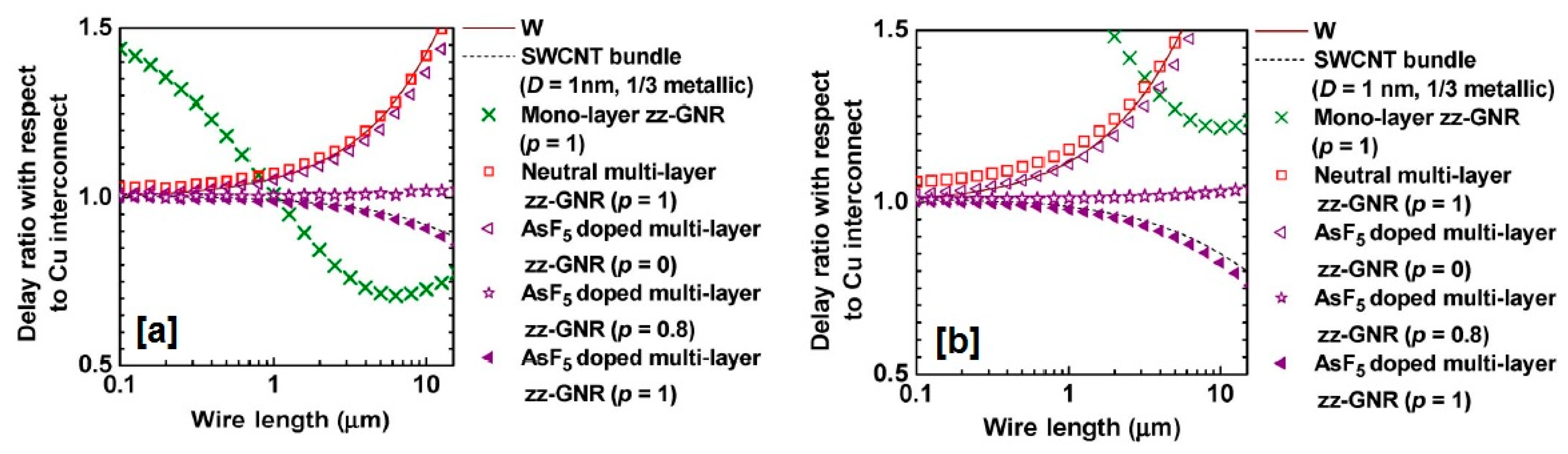
Considering the RLC model in Figure 5b, a delay was calculated in 11 nm technology by Xu et al. [8]. The delay calculations were done for the zz-GNR, zz-MLGNR, doped zz-MLGNR, W, and SWCNT bundle, and they were compared with the Cu interconnects (Figure 21). A similar study was carried out for the minimum driver size and double minimum driver size, and is shown in Figure 21a,b, respectively. The edge roughness is represented here in terms of specularity (p). The smooth edge signifies a complete specular edge (i.e., P = 1) or zero backscattering probability (i.e., P = 0).
The performance of the monolayer and multilayer zz-GNR is worse than Cu, even if a complete specular edge is assumed. The zz-MLGNR performs better than Cu only if it is doped (AsF5) by intercalation and the specular edge p > 0.8. The AsF5-doped zz-MLGNR may be slightly better than the SWCNT bundles if p = 1 can be achieved (Figure 21).
6.4. Crosstalk Effect
The integrated circuits consist of several adjacent interconnects, which are responsible for the generation of parasitic elements like mutual inductance and capacitance. Because of these parasitic components, a crosstalk effect is generated that can be considered as an extra serious matter in large scale integration [77,78]. The crosstalk phenomenon makes serious problem for the reliable operation of an interconnect, showing different effects like overshoot/undershoot [77], delay [79], glitch [78], and so on.
Figure 22a shows the cross-sectional view of the coupled MLGNR interconnects. To calculate the worst-case time-delay due to the crosstalk effect, the distributed RLC lines are drawn in Figure 22b, considering the parasitic coupling capacitor (CCdx) and inductor (Mdx). Now, CC = εt/s and M = µs/t denote the per-unit length values of the equivalent capacitance and mutual inductance induced by the coupling effects, where t and s are the MLGNR thickness and the distance between two interconnects [77,80].
A crosstalk delay is calculated in the literature [4] for neutral zz-MLGNR and AsF5 doped zz-MLGNR, considering ITRS technology node 8 nm and 11 nm, respectively. A crosstalk delay of MLGNR is compared with the Cu interconnect delay as a function of the interconnect length (l) for different specularity (p). A crosstalk delay is improved for the neutral and doped zz-MLGNR for all of the specularity compared to the Cu interconnects in a 8 nm technology node. In a 11 nm node, only doped zz-MLGNR shows an improved performance compared with the Cu interconnects for specularity p = 0.8 and 1.
6.5. Stability Analysis
A stability analysis is another performance criterion of multilayer GNR (MLGNR) interconnects. The analysis of the Nyquist stability and Bode stability by considering the distributed RLC model of the MLGNR interconnects is shown in this section [6,81].
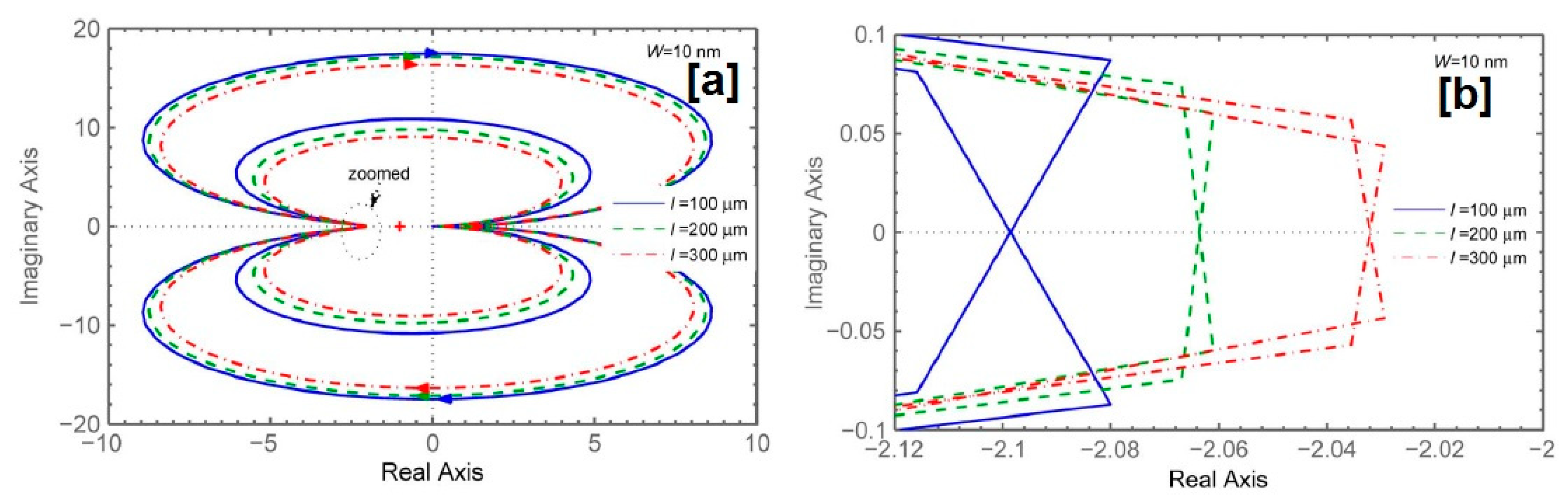
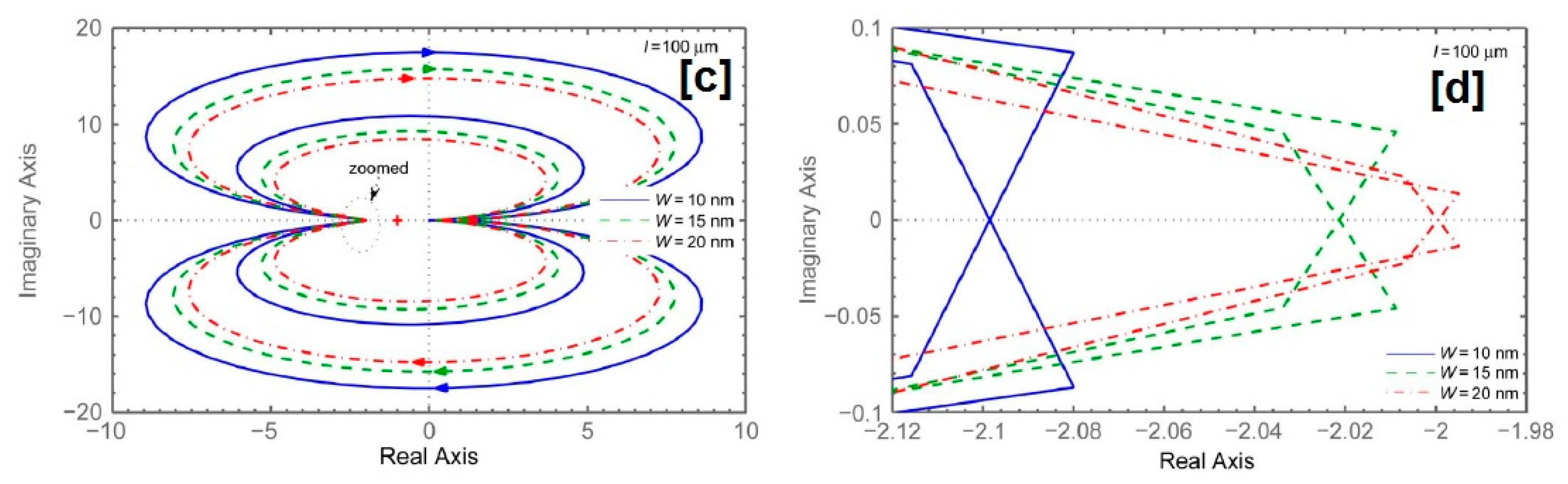
The Nyquist plot in a complex plane coordinates system can be considered as a powerful tool for investigating the system’s relative stability. The critical point (−1, 0), in the complex plane, is the critical point for stability. The point must move towards outside the diagram, showing a better stability of the system [81,82]. Figure 23a shows the Nyquist stability diagram for MLGNR interconnects of various lengths (100 µm < l < 300 µm) for a constant width (w) of 10 nm. Figure 23b shows the zoomed portion where a critical point is shifted outwards of the diagram for larger length MLGNR interconnects, showing its improved stability performance. The study was also repeated for a variable width of MLGNR (10 nm < w < 20 nm) for a constant length of 100 µm, as shown in Figure 23c. The zoomed portions of Figure 23c in Figure 23d clearly show the outwards shifting of the critical point for the larger width of MLGNR, showing its improved stability characteristics. So, the transmission line modeling along with the Nyquist stability diagram confirms that the relative stability of the MLGNR interconnects system increases with an increase of either the length or width [6,59].
A similar RLC model can be implemented for the Bode stability analysis of the MLGNR interconnects. The Bode stability can be measured from the gain margin (GM) and phase margin (PM) of a system. As the GM and PM are increased, the system stability increases. In the literature [63], the relative stability of Cu, TC-MLGNR, and SC-MLGNR are demonstrated by increasing the interconnect length from 10 to 100 µm, and varying the interconnect widths from 11 to 22 nm. Figure 24a,b show the GM and PM as a function of the interconnect length for a 16 nm ITRS technology node, where the GM and PM of the TC-GNR interconnect are very close to that of the Cu interconnect. In Figure 24c,d, the GM and PM are plotted as a function of the interconnect width for a 10 µm constant length. Here, the GM and PM are high in the TC-GNR interconnect compared with the Cu and SC-GNR interconnects. Similar to the Nyquist stability, the Bode stability analysis in Figure 24 also confirms that the relative stability increases when the interconnect length (l) and width (w) increase, and hence, the system becomes more stable. As the interconnect length is increased, the network delay increases. Then, the step response of all types of interconnects tends to damp more rapidly and the system becomes more stable [59].
7. Summary and Concluding Remarks
In this review, a systematic study has been carried out to analyze the potential application of graphene nanoribbons (GNRs) as one of the next generation of on-chip interconnects. The shape of the graphene nanoribbon has a strong impact on its electrical properties. While the armchair edge GNR shows semiconducting as well as metallic behavior, depending on the number of dimers, the zigzag edge GNR shows to be always semiconducting in nature. After studying the structural and electrical properties, synthesis, and fabrication techniques, the GNR interconnect has been explored in detail. The chemical vapor deposition (CVD) method is the popular technique for the synthesis of high quality mono- or multi-layer graphene film, and photolithography is the most suitable technique for patterning the GNRs with an appropriate width and length. As the conductivity of GNR strongly depends on its edge shape and edge roughness, the patterning of GNR from a graphene sheet is still a challenging task. GNR conductivity also depends on its number of layers. The mono layer shows a high resistivity, and the large number of layers show a graphitic nature with poor conductivity. So, only a few layer GNRs are suitable for interconnect applications, and therefore the controlled synthesis of GNR is of prime interest for the development of the technology for the replacement of conventional metal interconnects by GNR.
The electrical circuit modeling of GNR interconnects with the distributed RLC network is explored to relate its structural properties with electrical behavior. The model shows a strong dependence of conductivity of GNR on its width, especially below a 20 nm range. The mean free path (MFP) of suspended graphene is very high and close to 1 µm, but it is reduced significantly to roughly 100 nm on a SiO2 substrate because of charged impurity scattering and phonon scattering. MFP increases up to 300 nm for hexagonal boron nitride substrate. The conductivity of the GNR interconnects strongly depends on the backscattering probability of the electron near its edges. The conductance of the GNR interconnects increases significantly for complete specular edges (i.e., zero back scattering). The electrical resistance of a single layer graphene nanoribbon (GNR) is relatively high compared to Cu, whereas a multilayer GNR (MLGNR) offers a reduced equivalent resistance, which is more suitable for interconnect applications.
In a performance comparison of the GNR interconnects with Cu (aspect ratio 2), resistivity is found to be low in case of Cu above 10 nm in width. In a few cases, GNR shows better resistivity when w < 8–10 nm only. On the other hand, the GNR interconnects show low-value capacitance compared to the Cu interconnects, because of the extremely low thickness of the graphene film. Obviously, the capacitance increases with the increase in the number of layers of graphene. After comparing the resistive and capacitive properties of the GNR interconnects, a 50% RC delay is calculated and found to be lower than Cu for all of the cases when the edge backscattering probability for GNR is zero. The energy delay product (EDP) is also found to be lower in case of the specular edge GNR compared with the Cu interconnects. An improvised performance is also found for the GNR interconnects considering a high MFP of 1 µm. But, the GNR interconnects must have a non-zero edge backscattering probability with reduced MFP (<µm) on the substrates, like SiO2, BN, and so on, for practical implementations.
The performance of a few layers of GNR has been compared with single wall carbon nanotube (SWCNT) and doped MLGNR, and the overall better result has been found compared to single or multilayer GNR interconnects. If GNR is compared with SWCNT, the former has edge scattering, which reduces the effective MFP. From a fabrication point of view, the synthesis of GNR is more straight forward than SWCNT. Also, the chirality of GNR is not random like SWCNT. However, until now, doped GNR is the less explored area in the domain of interconnects.
In this review article, it is essentially concluded that the graphene nanoribbons (GNR) are far more suitable as an interconnect material for the fabrication of the most advanced electronic circuits and devices. The inherent superior properties of graphene instill the development of GNR interconnects. Furthermore, the article has revealed the merits of multilayer graphene nanoribbons (MLGNR), which are easier to fabricate and are more cost effective than single layer graphene nanoribbons (SLGNR). The article also reflects the enhanced performance of GNR as the on-chip interconnects, compared to the conventional metal interconnects, like Cu or W. The possible scientific interpretations have been put forward to convince the arguments in favor of the potential of recently developed graphene nanoribbons for efficient applications as on chip interconnects in the miniaturized advanced electronic circuits and devices.
Author Contributions
Authors contributed equally to this work.
Funding
This research received no external funding.
Acknowledgments
This work was supported in part by the Early Carrier Research grant (Lett. No. ECR/2015/000345) by SERB, Government of India, and the Additional Competitive Research Grant by BITS-Pilani, Rajasthan-333031, India.
Conflicts of Interest
The authors declare no conflict of interest.
References
- Hu, C. Future CMOS scaling and reliability. IEEE Proc. 1993, 81, 682–689. [Google Scholar] [CrossRef]
- Sze, S.M.; Ng, K.K. Physics of Semiconductor Devices, 3rd ed.; John Wiley and Sons: Hoboken, NJ, USA, 2007. [Google Scholar]
- Rakheja, S.; Kumar, V.; Naeemi, A. Evaluation of the potential performance of graphene nanoribbons as on-chip interconnects. Proc. IEEE 2013, 101, 1740–1765. [Google Scholar] [CrossRef]
- Sahoo, M.; Rahaman, H. Analysis of crosstalk-induced effects in multilayer graphene nanoribbon interconnects. J. Circuits Syst. Comput. 2017, 26, 1750102. [Google Scholar] [CrossRef]
- Naeemi, A.; Meindl, J.D. Compact physics-based circuit models for graphene nanoribbon interconnects. IEEE Trans. Electron Devices 2009, 569, 1822–1833. [Google Scholar] [CrossRef]
- Banerjee, K.; Mehrotra, A. Analysis of on-chip inductance effects for distributed RLC interconnects. IEEE Trans. Comput. Aided Des. Integr. Circuits Syst. 2002, 21, 904–915. [Google Scholar] [CrossRef]
- Kumar, V.; Rakheja, S.; Naeemi, A. Performance and energy-per-bit modeling of multilayer graphene nanoribbon conductors. IEEE Trans. Electron Devices 2012, 59, 2753–2761. [Google Scholar] [CrossRef]
- Xu, C.; Li, H.; Banerjee, K. Modeling analysis, and design of graphene nano-ribbon interconnects. IEEE Trans. Electron Devices 2009, 56, 1567–1572. [Google Scholar] [CrossRef]
- Murali, R.; Brenner, K.; Yang, Y.; Beck, T.; Meindl, J.D. Resistivity of graphene nanoribbon interconnects. IEEE Electron Device Lett. 2009, 30, 611–613. [Google Scholar] [CrossRef]
- Misawa, T.; Okanaga, T.; Mohamad, A.; Sakai, T.; Awano, Y. Line width dependence of transport properties in graphene nanoribbon interconnects with real space edge roughness determined by Monte Carlo method. Jpn. J. Appl. Phys. 2015, 54, 05EB01. [Google Scholar] [CrossRef]
- Meindl, J. Beyond Moore’s law: The interconnect era. Comput. Sci. Eng. 2003, 5, 20–24. [Google Scholar] [CrossRef]
- Im, S.; Srivastava, N.; Banerjee, K.; Goodson, K.E. Scaling analysis of multilevel interconnect temperatures for high-performance ICs. IEEE Trans. Electron Devices 2005, 52, 2710–2719. [Google Scholar] [CrossRef]
- Liu, B.; Liu, Y.; Shen, S. Thermal plasmonic interconnects in graphene. Phys. Rev. B 2014, 90, 195411. [Google Scholar] [CrossRef]
- Chen, J.H.; Jang, C.; Xiao, S.; Ishigami, M.; Fuhrer, M.S. Intrinsic and extrinsic performance limits of graphene devices on SiO2. Nat. Nanotechnol. 2008, 3, 206–2019. [Google Scholar] [CrossRef] [PubMed]
- Choi, W.; Lahiri, I.; Seelaboyina, R.; Kang, Y.S. Synthesis of graphene and its applications: A review. Solid State Mater. Sci. 2010, 35, 52–71. [Google Scholar] [CrossRef]
- Basu, S.; Bhattacharyya, P. Recent developments on graphene and graphene oxide based solid state gas sensor. Sens. Actuators B 2012, 173, 1–21. [Google Scholar] [CrossRef]
- Dutta, D.; Hazra, A.; Hazra, S.K.; Das, J.; Bhattacharyya, S.; Sarkar, C.K.; Basu, S. Performance of a CVD grown graphene-based planar device for a hydrogen gas sensor. Meas. Sci. Technol. 2015, 26, 115104. [Google Scholar] [CrossRef]
- Wang, X.; Ouyang, Y.; Jiao, L.; Wang, H.; Xie, L.; Wu, J.; Guo, J.; Dai, H. Graphene nanoribbons with smooth edges behave as quantum wires. Nat. Nanotechnol. 2011, 6, 563–568. [Google Scholar] [CrossRef] [PubMed]
- Nakada, K.; Fujita, M.; Dresselhaus, G.; Dresselhaus, M.S. Edge state in graphene ribbons: Nanometer size effect and edge shape dependence. Phys. Rev. B 1996, 54, 17954. [Google Scholar] [CrossRef]
- Kim, R.-H.; Bae, M.-H.; Kim, D.G.; Cheng, H.; Kim, B.H.; Kim, D.-H.; Li, M.; Wu, J.; Du, F.; Kim, H.-S.; et al. Stretchable, transparent graphene interconnects for arrays of microscale inorganic light emitting diodes on rubber substrates. Nano Lett. 2011, 11, 3881–3886. [Google Scholar] [CrossRef] [PubMed]
- Politou, M.; Asselberghs, I.; Soree, B.; Lee, C.S.; Sayan, S.; Lin, D.; Pashaei, P.; Huyghebaert, C.; Raghavan, P.; Radu, I.; et al. Single and multilayer graphene wires as alternative interconnects. Microelectron. Eng. 2016, 156, 131–135. [Google Scholar] [CrossRef]
- Agapito, L.A.; Kioussis, N. Seamless Graphene interconnects for the prospect of all-carbon spin-polarized field-effect transistors. J. Phys. Chem. C 2011, 115, 2874–2879. [Google Scholar] [CrossRef] [PubMed]
- Chin, H.C.; Lim, C.S.; Wong, W.S.; Danapalasingam, K.A.; Arora, V.K.; Tan, M.L.P. Enhanced device and circuit-level performance benchmarking of graphene nanoribbon field-effect transistor against a nano-MOSFET with interconnects. J. Nanomater. 2014, 2014, 879813. [Google Scholar] [CrossRef]
- Wakabayashi, K.; Fujita, M.; Ajiki, H.; Sigrist, M. Electronic and magnetic properties of nanographite ribbons. Phys. Rev. B 1999, 59, 8271. [Google Scholar] [CrossRef]
- Avouris, P.; Chen, Z.; Perebeinos, V. Carbon-based electronics. Nat. Nanotechnol. 2007, 2, 605–615. [Google Scholar] [CrossRef] [PubMed]
- Li, H.; Xu, C.; Srivastava, N.; Banerjee, K. Carbon nanomaterials for next-generation interconnects and passives: Physics, status, and prospects. IEEE Trans. Electron Devices 2009, 56, 1799–1821. [Google Scholar] [CrossRef]
- Ghosh, K.; Ranjan, N.; Verma, Y.K.; Tan, C.S. Graphene–CNT hetero-structure for next generation interconnects. RSC Adv. 2016, 6, 53054–53061. [Google Scholar] [CrossRef]
- Jiang, J.; Kang, J.; Cao, W.; Xie, X.; Zhang, H.; Chu, J.H.; Liu, W.; Banerjee, K. Intercalation doped multilayer-graphene-nanoribbons for next-generation interconnects. Nano Lett. 2017, 17, 1482–1488. [Google Scholar] [CrossRef] [PubMed]
- Zhao, R.; Afaneh, T.; Dharmasena, R.; Jasinski, J.; Sumanasekera, G.; Henner, V. Study of nitrogen doping of graphene via in-situ transport measurements. Physica B 2016, 490, 21–24. [Google Scholar] [CrossRef]
- Wu, X.; Asselberghs, I.; Politou, M.; Contino, A.; Radu, I.; Huyghebaert, C.; Tokei, Z.; Soree, B.; Gendt, S.D.; Feyter, S.D.; et al. Doping of graphene for the application in nano-interconnect. Microelectron. Eng. 2017, 167, 42–46. [Google Scholar] [CrossRef]
- Wakabayashi, K.; Dutta, S. Nanoscale and edge effect on electronic properties of graphene. Solid State Commun. 2012, 152, 1420–1430. [Google Scholar] [CrossRef]
- Yu, Q.; Lian, J.; Siriponglert, S.; Li, H.; Chen, Y.P.; Pei, S.-S. Graphene segregated on Ni surfaces and transferred to insulators. Appl. Phys. Lett. 2008, 93, 113103. [Google Scholar] [CrossRef] [Green Version]
- Naeemi, A.; Meindl, J.D. Conductance modeling for graphene nanoribbon (GNR) interconnects. IEEE Electron. Device Lett. 2007, 28, 428–431. [Google Scholar] [CrossRef]
- Chen, P.-A.; Chiang, M.-H.; Hsu, W.-C. All-zigzag graphene nanoribbons for planar interconnect application. J. Appl. Phys. 2017, 122, 034301. [Google Scholar] [CrossRef]
- Dorf, R.C.; Bishop, R.H. Modern Control. System, 11th ed.; Prentice-Hall Press: Upper Saddle River, NJ, USA, 2008. [Google Scholar]
- Maffucci, A.; Miano, G. Transmission line model of graphene nanoribbon interconnects. Nanosci. Nanotechnol. Lett. 2013, 5, 1207–1216. [Google Scholar] [CrossRef]
- Bischoff, D.; Varlet, A.; Simonet, P.; Eich, M.; Overweg, H.C.; Ihn, T.; Ensslin, K. Localized charge carriers in graphene nanodevices. Appl. Phys. Rev. 2015, 2, 031301. [Google Scholar] [CrossRef] [Green Version]
- Maffucci, A.; Miano, G. Electrical properties of graphene for interconnect applications. Appl. Sci. 2014, 4, 305–317. [Google Scholar] [CrossRef]
- Son, Y.-W.; Cohen, M.L.; Louie, S.G. Energy gaps in graphene nanoribbons. Phys. Rev. Lett. 2006, 97, 216803. [Google Scholar] [CrossRef] [PubMed]
- Gopar, V.A. Reprint of: Shot noise fluctuations in disordered graphene nanoribbons near the Dirac point. Physica E 2016, 82, 79–84. [Google Scholar] [CrossRef]
- Reich, S.; Maultzsch, J.; Thomsen, C. Tight-binding description of graphene. Phys. Rev. B 2002, 66, 035412. [Google Scholar] [CrossRef]
- Schmidt, M.E.; Hammam, A.M.M.; Iwasaki, T.; Kanzaki, T.; Muruganathan, M.; Ogawa, S.; Mizuta, H. Controlled fabrication of electrically contacted carbon nanoscrolls. Nanotechnology 2018, 29, 235605. [Google Scholar] [CrossRef] [PubMed] [Green Version]
- Victor, A.; Ermakov, V.A.; Alaferdov, A.V.; Vaz, A.R.; Perim, E.; Autreto, P.A.S.; Paupitz, R.; Galvao, D.S.; Moshkalev, S.A. Burning Graphene Layer-by-Layer. Sci. Rep. 2015, 5, 11546. [Google Scholar] [Green Version]
- Meyer, J.C.; Geim, A.K.; Katsnelson, M.I.; Novoselov, K.S.; Booth, T.J.; Roth, S. The structure of suspended graphene sheets. Nature 2007, 446, 60–63. [Google Scholar] [CrossRef] [PubMed] [Green Version]
- Yagmurcukardes, M.; Peeters, F.M.; Senger, R.T.; Sahin, H. Nanoribbons: From fundamentals to state-of-the-art applications. Appl. Phys. Rev. 2016, 3, 041302. [Google Scholar] [CrossRef] [Green Version]
- Politou, M.; Wu, X.; Asselberghs, I.; Contino, A.; Soree, B.; Radu, I.; Huyghebaert, C.; Tokei, Z.; Gendt, S.D.; Heyns, M. Evaluation of multilayer graphene for advanced interconnects. Microelectron. Eng. 2017, 167, 1–5. [Google Scholar] [CrossRef]
- Behnam, A.; Lyons, A.S.; Bae, M.-H.; Chow, E.K.; Islam, S.; Neumann, C.M.; Pop, E. Transport in nanoribbon interconnects obtained from graphene grown by chemical vapor deposition. Nano Lett. 2012, 12, 4424–4430. [Google Scholar] [CrossRef] [PubMed]
- Li, X.; Magnuson, C.W.; Venugopal, A.; An, J.; Suk, J.W.; Han, B.; Borysiak, M.; Cai, W.; Velamakanni, A.; Zhu, Y.; et al. Graphene films with large domain size by a two-step chemical vapor deposition process. Nano Lett. 2010, 10, 4328–4334. [Google Scholar] [CrossRef] [PubMed]
- Xu, W.; Lim, T.-S.; Seo, H.-K.; Min, S.-Y.; Ho, H.C.; Park, M.-H.; Kim, Y.-H.; Lee, T.-W. N-doped graphene field-effect transistors with enhanced electron mobility and air-stability. Small 2014, 10, 1999–2005. [Google Scholar] [CrossRef] [PubMed]
- Lu, Y.-F.; Lo, S.-T.; Lin, J.-C.; Zhang, W.; Lu, J.-Y.; Liu, F.-H.; Tseng, C.-M.; Lee, Y.; Liang, C.-T.; Li, L.-J. Nitrogen-doped graphene sheets grown by chemical vapor deposition: Synthesis and influence of nitrogen impurities on carrier transport. ACS Nano 2013, 7, 6522–6532. [Google Scholar] [CrossRef] [PubMed]
- Chang, D.-W.; Lee, E.K.; Park, E.Y.; Yu, H.; Choi, H.-J.; Jeon, I.-Y.; Sohn, G.-J.; Shin, D.; Park, N.; Oh, J.-H.; et al. Nitrogen-doped graphene nanoplatelets from simple solution edge-functionalization for n-type field-effect transistors. J. Am. Chem. Soc. 2013, 135, 8981–8988. [Google Scholar] [CrossRef] [PubMed]
- Chen, X.; Akinwande, D.; Lee, K.-J.; Close, G.F.; Yasuda, S.; Paul, B.C.; Fujita, S.; Kong, J.; Philip, W.H.-S. Fully integrated graphene and carbon nanotube interconnects for gigahertz high-speed CMOS electronics. IEEE Trans. Electron. Devices 2010, 57, 3137–3143. [Google Scholar] [CrossRef]
- Lee, W.; Jang, H.; Jang, B.; Kim, J.-H.; Ahn, J.-H. Stretchable Si logic device with graphene interconnects. Mater. View 2015, 11, 6272–6277. [Google Scholar] [CrossRef] [PubMed]
- Ferrari, A.C.; Basko, D.M. Raman spectroscopy as a versatile tool for studying the properties of graphene. Nat. Nanotechnol. 2013, 8, 235–246. [Google Scholar] [CrossRef] [PubMed] [Green Version]
- Ryu, S.; Maultzsch, J.; Han, M.Y.; Kim, P.; Brus, L.E. Raman spectroscopy of lithographically patterned graphene nanoribbons. ACS Nano 2011, 5, 4123–4130. [Google Scholar] [CrossRef] [PubMed]
- Ci, L.; Xu, Z.; Wang, L.; Gao, W.; Ding, F.; Kelly, K.F.; Yakobson, B.I.; Ajayan, P.M. Controlled nanocutting of graphene. Nano Res. 2008, 1, 116–122. [Google Scholar] [CrossRef]
- Han, M.Y.; Ozyilmaz, B.; Zhang, Y.; Kim, P. Energy band-gap engineering of graphene nanoribbons. Phys. Rev. Lett. 2007, 98, 206805. [Google Scholar] [CrossRef] [PubMed]
- Datta, S. Quantum Transport: Atom to Transistor; Cambridge University Press: Cambridge, UK, 2005. [Google Scholar]
- Nasiri, S.H.; Moravvej-Farshi, M.K.; Faez, R. Stability analysis in graphene nanoribbon interconnects. IEEE Electron. Device Lett. 2010, 31, 1458–1460. [Google Scholar] [CrossRef]
- Naeemi, A.; Meindl, J.D. Design and performance modeling for single-walled carbon nanotubes as local, semiglobal, and global interconnects in gigascale integrated systems. IEEE Trans. Electron. Devices 2007, 54, 26–37. [Google Scholar] [CrossRef]
- Fotoohi, S.; Haji-Nasiri, S. Transfer matrix model of multilayer graphene nanoribbon interconnects. Microelectron. Reliab. 2017, 79, 193–200. [Google Scholar] [CrossRef]
- Ferry, D.K.; Goodnick, S.M. Transport in Nanostructures; Cambridge University Press: Cambridge, UK, 1997. [Google Scholar]
- Bhattacharya, S.; Das, D.; Rahaman, H. Stability analysis in top-contact and side-contact graphene nanoribbon interconnects. IETE J. Res. 2017, 63, 588–596. [Google Scholar]
- Shao, Q.; Liu, G.; Teweldebrhan, D.; Balandin, A.A. High-temperature quenching of electrical resistance in graphene Interconnects. Appl. Phys. Lett. 2008, 92, 202108. [Google Scholar] [CrossRef]
- Zhao, W.-S.; Yin, W.-Y. Comparative study on multilayer graphene nanoribbon (MLGNR) interconnects. IEEE Trans. Electromagn. Compat. 2014, 56, 638–645. [Google Scholar] [CrossRef]
- Nishad, A.K.; Sharma, R. Analytical time-domain models for performance optimization of multilayer GNR interconnects. IEEE J. Sel. Top. Quantum Electron. 2014, 20, 17–24. [Google Scholar] [CrossRef]
- Wang, X.; Ouyang, Y.; Li, X.; Wang, H.; Guo, J.; Dai, H. Room-temperature all-semiconducting sub-10-nm graphene nanoribbon field-effect transistors. Phys. Rev. Lett. 2008, 100, 206803. [Google Scholar] [CrossRef] [PubMed]
- Jain, N.; Durcan, C.A.; Jacobs-Gedrim, R.; Xu, Y.; Yu, B. Graphene interconnects fully encapsulated in layered insulator hexagonal boron nitride. Nanotechnology 2013, 24, 355202. [Google Scholar] [CrossRef] [PubMed]
- Dean, C.R.; Young, A.F.; Meric, I.; Lee, C.; Wang, L.; Sorgenfrei, S.; Watanabe, K.; Taniguchi, T.; Kim, P.; Shepard, K.L.; et al. Boron nitride substrates for high-quality graphene electronics. Nat. Nanotechnol. 2010, 5, 722–726. [Google Scholar] [CrossRef] [PubMed] [Green Version]
- Sui, Y.; Appenzeller, J. Screening and interlayer coupling in multilayer graphene field-effect transistors. Nano Lett. 2009, 9, 2973–2977. [Google Scholar] [CrossRef] [PubMed]
- Soldano, C.; Talapatra, S.; Kar, S. Carbon nanotubes and graphene nanoribbons: Potentials for nanoscale electrical interconnects. Electronics 2013, 2, 280–314. [Google Scholar] [CrossRef]
- Yang, Y.; Murali, R. Impact of size effect on graphene nanoribbon transport. IEEE Electron. Device Lett. 2010, 31, 237–239. [Google Scholar] [CrossRef]
- Berger, C.; Song, Z.; Li, T.; Li, X.; Ogbazghi, A.Y.; Feng, R.; Dai, Z.; Marchenkov, A.N.; Conrad, E.H.; First, P.N.; et al. Ultrathin epitaxial graphite: 2D electron gas properties and a route toward graphene-based nanoelectronics. J. Phys. Chem. B 2004, 108, 19912–19916. [Google Scholar] [CrossRef]
- Obradovic, B.; Kotlyar, R.; Heinz, F.; Matagne, P.; Rakshit, T. Analysis of graphene nanoribbons as a channel material for field-effect transistors. Appl. Phys. Lett. 2006, 88, 142102. [Google Scholar] [CrossRef]
- Ohta, T.; Bostwick, A.; Seyller, T.; Horn, K.; Rotenberg, E. Controlling the electronic structure of bilayer graphene. Science 2006, 313, 951–954. [Google Scholar] [CrossRef] [PubMed]
- Pan, C.; Raghavan, P.; Ceyhan, A.; Catthoor, F.; Tokei, Z.; Naeemi, A. Technology/Circuit/System Co-optimization and Benchmarking for Multilayer Graphene Interconnects at Sub-10-nm Technology Node. IEEE Trans. Electron. Devices 2015, 62, 1530–1536. [Google Scholar]
- Bagheri, A.; Ranjbar, M.; Haji-Nasiri, S.; Mirzakuchaki, S. Crosstalk bandwidth and stability analysis in graphene nanoribbon interconnects. Microelectron. Reliab. 2015, 55, 1262–1268. [Google Scholar] [CrossRef]
- Sakurai, T. Closed-form expressions for interconnection delay coupling, and crosstalk in VLSI’s. IEEE Trans. Electron. Devices 1993, 40, 118–124. [Google Scholar] [CrossRef]
- Nieuwoudt, A.; Kawa, J.; Massoud, Y. Crosstalk-induced delay, noise, and interconnect planarization implications of fill metal in nanoscale process technology. IEEE Trans. Very Large Scale Integr. (VLSI) Syst. 2010, 18, 378–391. [Google Scholar] [CrossRef]
- Mekala, G.K.; Agrawal, Y.; Chandel, R. Modelling and performance analysis of dielectric inserted side contact multilayer graphene nanoribbon interconnects. IET Circuits Device Syst. 2017, 11, 232–240. [Google Scholar] [CrossRef]
- Farrokhi, M.; Faez, R.; Nasiri, S.H.; Davoodi, B. Effect of Varying Aspect Ratio on Relative Stability for Graphene Nanoribbon Interconnects. Appl. Mech. Mater. 2012, 229, 205–209. [Google Scholar] [CrossRef]
- Fathi, D.; Forouzandeh, B.; Mohajerzadeh, S.; Sarvari, R. Accurate analysis of carbon nanotube interconnects using transmission line model. Micro Nano Lett. 2009, 4, 116–121. [Google Scholar] [CrossRef]
Figure 1.
Schematic of on-chip interconnects parallel to the ground plane showing all parasitic capacitances.
Figure 1.
Schematic of on-chip interconnects parallel to the ground plane showing all parasitic capacitances.

Figure 2.
Structure of graphene nanoribbons with (a) armchair edges (armchair ribbon) and (b) zigzag edges (zigzag ribbon) [31]. Reproduced with permission from [31]. Elsevier, 2012.

Figure 3.
Energy band structure of (a) armchair nanoribbon with N = 50 and (b) zigzag nanoribbons with N = 30 [31]. Reproduced with permission from [31]. Elsevier, 2012.

Figure 4.
Variation of the band gap of armchair graphene nanoribbons (GNRs) as a function of the width (w) obtained (a) from tight binding (TB) calculations with t = 2.70 eV (nearest neighbor hoping integral) and (b) from first-principles calculations within the local-density approximation (LDA) [39]. The number of dimer N is represented as Na in this figure. Reproduced with permission from [39]. The American Physical Society, 2006.

Figure 5.
(a) Schematic of graphene growth by the chemical vapor deposition (CVD) method and GNR fabrication process; (b) Scanning electron microscope (SEM) image of a GNR between Ti/Au electrodes; (c) Atomic force microscope (AFM) image of AlOx covering a GNR (W ∼ 60 nm); (d) AFM image of AlOx free GNR (W ∼ 35 nm); (e) Cross section of AFM profile along dashed line shown in (d), showing the GNR thickness in the range 1–1.2 nm; (f) Presents the Raman spectra (excitation wavelength 633 nm) [47]. Reproduced with permission from [47]. The American Physical Society, 2012.

Figure 6.
(a) Schematic of multilayer (ML)-graphene growth on Cu–Ni alloy; (b) Transferred ML-graphene on SiO2 substrate followed by oxygen plasma etching with Ni line mask; (c) FeCl3 intercalation doping at 633 K; (d) Four-probe test structures; SEM images of (e) four-probe test structure with patterned GNR; (f–h) GNRs with 20.6, 84.1, and 280 nm width. AFM image of (i) undoped ML-graphene and (j) 10 h FeCl3 intercalation doped ML-graphene, indicating a 20% increase in thickness after doping; The Raman spectrum of (k,n) undoped ML-graphene, (l,o) FeCl3 intercalation doped ML-graphene and (m) FeCl3. Reproduced with permission from [28]. The American Physical Society, 2016.

Figure 7.
Process flows of as-fabricated on-chip graphene interconnect. (a) Transfer of CVD-grown graphene to target substrate; (b) integration of graphene with complementary metal oxide semiconductor (CMOS) circuitry; (c) optical image of CMOS ring oscillator array locating graphene sheet; (d) optical image of one fabricated graphene interconnect on top of the CMOS ring oscillator array. (Inset) AFM image of graphene stripes [52]. Reproduced with permission from [52]. IEEE, 2010.

Figure 8.
(a) Structure of single layer graphene interconnect; (b) resistive-inductive-capacitive (RLC) model for a single layer GNR interconnect [5]. Reproduced with permission from [5]. IEEE, 2009.

Figure 9.
Conductance of (a) metallic armchair GNRs and (b) semiconducting armchair GNRs as function of width (w) of graphene nanoribbons [5]. Reproduced with permission from [5]. IEEE, 2009.

Figure 10.
Schematic of multilayer graphene nanoribbon (MLGNR) interconnects with equivalent resistive network for (a) Top contact (TC) technology and (b) side contact (SC) technology.
Figure 10.
Schematic of multilayer graphene nanoribbon (MLGNR) interconnects with equivalent resistive network for (a) Top contact (TC) technology and (b) side contact (SC) technology.

Figure 11.
Resistance per unit length (Ω/µm) versus width (w) of GNRs, single wall carbon nanotube (SWCNT), and Cu [33]. Reproduced with permission from [33]. IEEE, 2007.

Figure 12.
Resistance per unit length of GNRs plotted as a function of width comparing with Cu and SWCNT. (a) Armchair GNRs for smooth edge; (b) zigzag GNRs for smooth edge; (c) rough edge GNRs with backscattered probability P = 0, 0.2, and 1 [5]. Reproduced with permission from [5]. IEEE, 2009.

Figure 13.
(a) SEM image of a set of ten GNRs between each electrode pair; (b) Performance of individual GNRs of various line widths. The equivalent Cu resistivity is shown by a star [9]. Reproduced with permission from [9]. IEEE, 2009.

Figure 14.
Measured resistivity (a) undoped multilayer GNRs (MLGNRs); (b) 10 h FeCl3 intercalation doped MLGNRs; (c) comparative performance between the doped MLGNR with 12 nm thickness, Cu wire with 12 nm thickness, and Cu wire with aspect ratio (AR) of two [28]. Reproduced with permission from [28]. The American Chemical Society, 2016.

Figure 15.
Resistance comparison of SWCNT bundles, mono-layer zigzag (zz)-GNR, ML-zz-GNR, tungsten (W) and AsF5 doped ML-zz-GNR as (a) global and (b) local interconnects. W is not considered for global wires because of its high resistivity [8]. Reproduced with permission from [8]. IEEE, 2009.

Figure 16.
Capacitance per unit length of graphene sheet consisting of different numbers of graphene layer as a function of width [76]. Reproduced with permission from [76]. IEEE, 2015.

Figure 17.
(a) Cross section of Cu and MLGNR. For ITRS 9.5 technology node, w = 9.5 nm, s = 9.5 nm, t = 20 nm, and h = 20 nm. The thickness of GNR depends on the number of layers, t′ = 0.35 × (2N − 1) nm. Dielectric constant for International Technology Roadmap for Semiconductors (ITRS) 9.5 node is 1.85; (b) Equivalent distribution of resistive-capacitive (RC) circuit of the driver-interconnect-load system [7]. Here, RS and CS are the source resistance and capacitance. RC1 and RC2 are the resistances at the two contacts. rw and cw are the per-unit-length resistance and capacitance of the interconnect, respectively. CL is the load capacitance, and Nch is the numbers of conduction channels in the topmost layer of MLGNR interconnect. Reproduced with permission from [7]. IEEE, 2012.

Figure 18.
(a) Delay versus number of layers and (b) energy delay product (EDP) versus number of layers for top and side contacts [3]. Reproduced with permission from [3]. IEEE, 2013.

Figure 19.
Impact of dimensional scaling on the delays of Cu and MLGNR interconnects with different driver sizes (L) and different edge-scattering probability (P). (a) L = 10, P = 0; (b) L = 10; P = 0.2; (c) L = 50, P = 0; (d) L = 50, P = 0.2 [7]. Reproduced with permission from [7]. IEEE, 2012.

Figure 20.
EDP of Cu and MLGNR interconnects as a function of interconnect length [7]. Reproduced with permission from [7]. IEEE, 2012.

Figure 21.
Delay ratio with respect to Cu wire (local interconnect = 11 nm, aspect ratio = 2.1), with (a) minimum driver size and (b) double the minimum driver size [8]. Reproduced with permission from [8]. IEEE, 2012.

Figure 22.
(a) Schematic of coupled MLGNR interconnects on a ground plane; (b) equivalent RLC interconnect lines showing coupling capacitor (Ccdx) and inductor (Mdx) [77,80].

Figure 23.
Nyquist diagrams for the distributed RLC model of MLGNR interconnect (a) for w = 10 nm and 100 μm ≤ l ≤ 300 μm; (b) zoomed in portion of the diagram (a) surrounded by the circle; (c) for l = 100 µm and 10 μm ≤ w ≤ 20 nm; (b) zoomed in portion of the diagram (c) surrounded by the circle [59]. Reproduced with permission from [59]. IEEE, 2010.


Figure 24.
Bode stability analysis for Cu, TC-GNR, and SC-GNR interconnects. (a) Gain margin (dB) and (b) phase margin (degree) vs. interconnect length plot of at 16 nm technology node; (c) Gain margin (dB) and (d) phase margin (degree) vs. interconnect width (w) plot at 10 µm length [63]. Reproduced with permission from [63]. IEEE, 2017.

© 2018 by the authors. Licensee MDPI, Basel, Switzerland. This article is an open access article distributed under the terms and conditions of the Creative Commons Attribution (CC BY) license (http://creativecommons.org/licenses/by/4.0/).
Share and Cite
MDPI and ACS Style
Hazra, A.; Basu, S. Graphene Nanoribbon as Potential On-Chip Interconnect Material—A Review. C 2018, 4, 49. https://0-doi-org.brum.beds.ac.uk/10.3390/c4030049
AMA Style
Hazra A, Basu S. Graphene Nanoribbon as Potential On-Chip Interconnect Material—A Review. C. 2018; 4(3):49. https://0-doi-org.brum.beds.ac.uk/10.3390/c4030049
Chicago/Turabian StyleHazra, Arnab, and Sukumar Basu. 2018. "Graphene Nanoribbon as Potential On-Chip Interconnect Material—A Review" C 4, no. 3: 49. https://0-doi-org.brum.beds.ac.uk/10.3390/c4030049
Note that from the first issue of 2016, this journal uses article numbers instead of page numbers. See further details here.