Two-Dimensional Carbon: A Review of Synthesis Methods, and Electronic, Optical, and Vibrational Properties of Single-Layer Graphene


1
Dipartimento di Fisica e Chimica—Emilio Segrè, Università degli Studi di Palermo, Via Archirafi 36, 90123 Palermo, Italy
2
Dipartimento di Fisica e Astronomia—Ettore Majorana, Università degli Studi di Catania, Via Santa Sofia 64, 95123 Catania, Italy
3
ATeN Center, Università degli Studi di Palermo, Viale delle Scienze, Edificio 18, 90128 Palermo, Italy
4
Consiglio Nazionale delle Ricerche-Istituto per la Microelettronica e Microsistemi, Strada VIII 5, 95121 Catania, Italy
*
Author to whom correspondence should be addressed.
C 2019, 5(4), 67; https://0-doi-org.brum.beds.ac.uk/10.3390/c5040067
Submission received: 2 August 2019
/
Revised: 15 October 2019
/
Accepted: 17 October 2019
/
Published: 1 November 2019
(This article belongs to the Special Issue Optical and Electronic Properties of Carbon-Based Nanomaterials and Composites)
Abstract
:Graphite has been widely used by humans for a large part of their history. Nevertheless, it has only recently been possible to isolate its basic unit: carbon atoms arranged in a honeycomb structure on a single plane, namely graphene. Since its discovery, many techniques have been developed and improved to properly synthesize graphene and its derivatives which are part of the novel class of two-dimensional materials. These advanced materials have imposed themselves in nanotechnology thanks to some outstanding physical properties due to their reduced dimensions. In the case of graphene, its reduced dimension gives rise to a high electrical mobility, a large thermal conductivity, a high mechanical resistance, and a large optical transparency. Therefore, such aspect is of great scientific interest for both basic and applied research, ranging from theoretical physics to surface chemistry and applied solid state physics. The connection between all these fields is guaranteed by spectroscopy and especially by Raman spectroscopy which provides a lot of information about structural and electronic features of graphene. In this review, the authors present a systematized collection of the most important physical insights on the fundamental electronic and vibrational properties of graphene, their connection with basic optical and Raman spectroscopy, and a brief overview of main synthesis methods.
1. Introduction
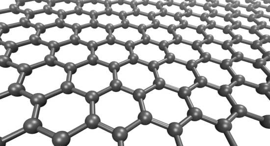
First observed in 2004 [1], graphene has rapidly established a key role in the branch of material science which concerns the investigation of nanomaterials [2]. Its outstanding electrical and thermal transport performance, wide optical transparency, and high mechanical resistance combined with structural flexibility make graphene an interesting material for several applications [3,4,5]. Some remarkable examples are solar cells and flexible capacitive systems [3,6,7,8,9], field effect, radio-frequency, and vertical THz transistors [10,11,12], and volatile memories [13]. Moreover, the discovery of graphene represented a real turning point also for basic sciences, having unveiled the existence of two-dimensional materials. According to IUPAC, graphene is defined as a single layer of graphite which is one of the main macroscopic allotropes of carbon [14]. As depicted in Figure 1a, graphene can be described as a polycyclic aromatic hydrocarbon molecule of quasi-infinite extension [14]. In particular, graphene is ideally composed by only carbon atoms arranged in a honeycomb structure that is a hexagonal lattice extending in a single sheet of atoms. Therefore, the key feature of this material consists of a two-dimensional structure which, as described below, is at the basis of the extraordinary properties of graphene. Since its on plane extension can be very large compared to its nanometric thickness (the lateral size of graphene can easily overcome the thickness by more than three orders of magnitude), graphene cannot be properly considered neither a large molecule, nor a bulk material, but it falls into the large family of nanomaterials similarly to all other two-dimensional materials. Even if the nomenclature of nano-size world is not yet well defined, nanomaterials are those materials in which at least one external or internal dimension is on the scale of nanometer [15,16].
In addition to this fundamental property, nanomaterials are classified according to various factors: constituent elements, characteristic dimensionality, and elementary or composite structure [15,16,17]. The categories in which graphene can be included are:
- Carbon-Based Nanomaterials
- Low-Dimensional Materials
- concerning materials whose nanometric scale implies a reduced dimensionality (that is the presence of at least one dimension which is much smaller to the other ones), which gives rise to some peculiar properties. Therefore, beyond a classic three-dimensional material, two-, one-, and zero-dimensional nanomaterials can be found [15,16].
For the latter class, it is important to notice that the limited dimensionality of the materials is not just a fancy feature, but a fundamental aspect which implies peculiar behaviors and properties for nanomaterials which are unknown for the macroscopic case [19]. Basing on the cited examples, every possible low-dimensional system is well represented by some carbon-based nanomaterials. The capability of carbon to assemble itself in so different structures derives from different number and structure of possible bonds which feature this element. Accordingly, the investigation of carbon electronic structure is the starting point to understand the structure, the properties of carbon-based nanomaterials, and in particular, of graphene.
The most important features of graphene are already reported in a plethora of review articles well focused on a specific subject [3,20,21,22,23,24,25]. Nevertheless, the authors aim to provide herein a systematized presentation of selected topics, in order to lead the reader from the fundamentals of carbon chemistry to the most important features of the electronic, optical and vibrational properties of graphene. In particular, an entire section is dedicated to the application of Raman spectroscopy in the investigation of several structural and electronic features of graphene. Therefore, the present review starts from a discussion of the basic chemical properties of carbon which determine various carbon-based nanomaterials, as well as their different structural features (Section 2). After that, a detailed description of the electronic band structure of graphene is given (Section 3) according to the tight-binding method described by Saitio et al. [26]. On the basis of this information, the optical properties of graphene are discussed (Section 4) by systematizing information collected in a former review by Mark et al. [22]. Thence, the discussion concerns the vibrational properties of graphene (Section 5), with particular attention to Raman scattering processes occurring in this material. In addition, a detailed section is dedicated to all the main factors which influence the Raman spectrum of graphene (Section 6). Thus, the review is completed by a brief discussion of the most common methods of synthesis currently used (Section 7).
2. Carbon
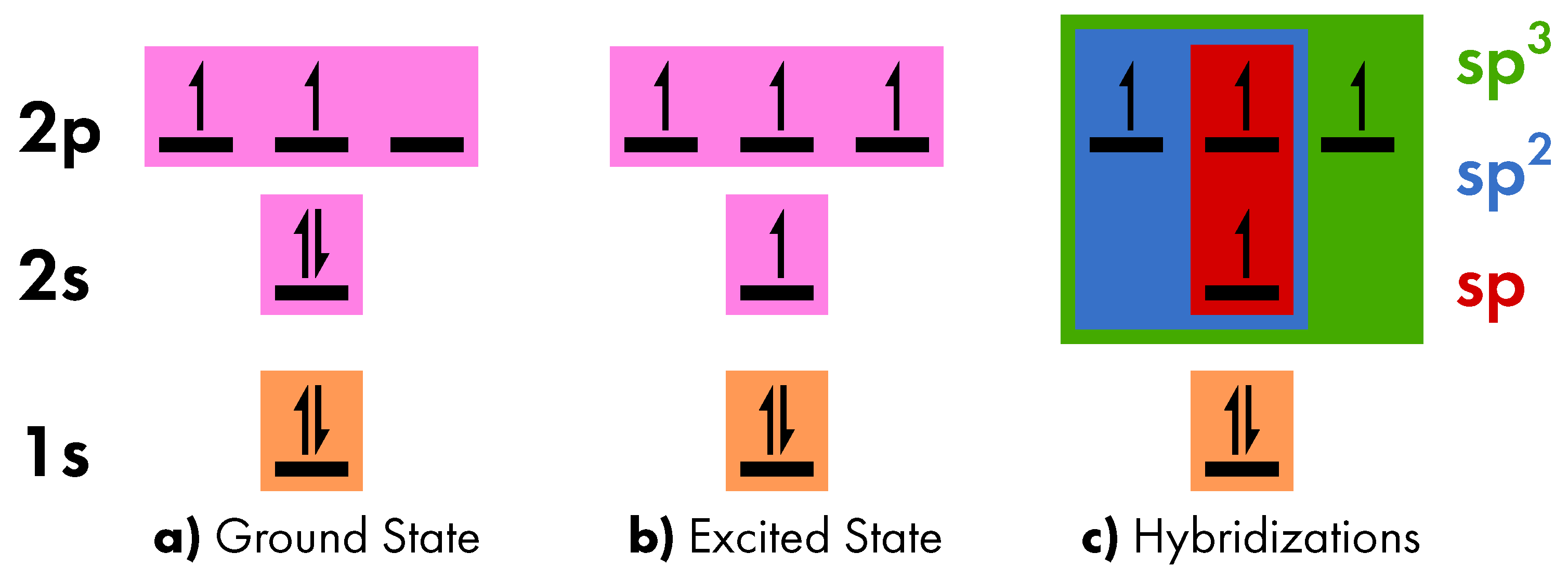
Carbon is one of the most abundant elements on Earth, and since it is at the basis of organic compounds, the known biology is based on it [27]. Its chemical fortune is due to a peculiar propensity to allotropy. In fact, carbon shows a peculiar variability in bonding both in bulk material and in molecular structures (from two to four bonds with other atoms can subsist, of single, double or triple order), thus determining many possible compounds and molecular species based on this element [28,29]. Carbon is the sixth chemical element of the periodic table, featured by atomic number 6, and its electronic configuration is thereby with four electrons available to form covalent chemical bonds. The electronic configuration of carbon at the ground state, whose energy distribution is reported in Figure 2a, is (1s2)2s22p2 [30]. Valence electrons are thereby placed in the 2s orbitals and in the degenerate 2p orbitals. Since only these electrons can be shared with other atomic species, a maximum of four electrons are theoretically available to form covalent chemical bonds [31]. By also considering the excited state, in which one electron is promoted from 2s atomic orbital to the last free 2p orbital (Figure 2b) only two or four electrons seem to be available for bonds. However, this prediction proves wrong, by contrasting the experimental evidence both in bond number and in incorrect orientations. Therefore, the bare atomic orbitals obtained for hydrogen result inadequate for a valid description of carbon bonds.
A better description is obtained by considering the presence of hybrid orbitals for valence electrons of carbon [18,29]. These orbitals are defined as combination of several simple atomic orbitals whose mixing is enabled by the slight energy difference between them [31,32]. As depicted in Figure 2c, three possible schemes are compatible with the electronic configuration of carbon [30,31]:
- sp hybridization
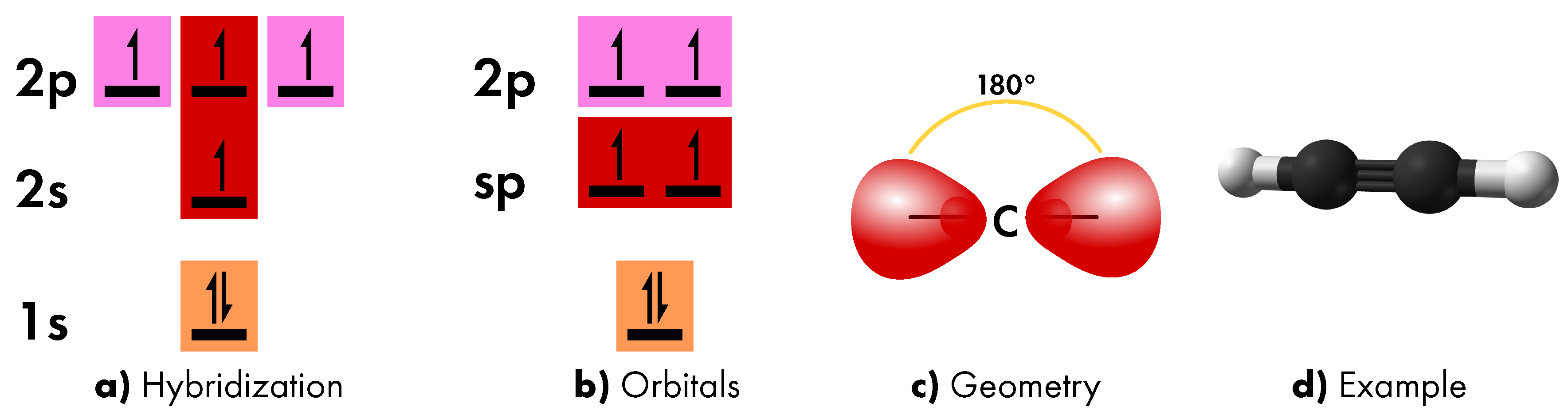
- which involves the 2s orbital and a single 2p orbital (Figure 3a). The resulting two hybrid orbitals are placed at intermediate energy (Figure 3b), are characterized by asymmetric lobes (due to the 2p contribution), and aligned on a single axis, thus assuming a linear geometry (Figure 3c). In the formation of molecular bonds, the sp orbitals contribute to the formation of a triple bond together with two remaining 2p orbitals, as in ethyne molecule. In this case, two carbon atoms share the electron of one sp orbital to form one σ bond and the electrons of both the remaining 2p orbitals to form a π bonds (Figure 3d).
- sp2 hybridization
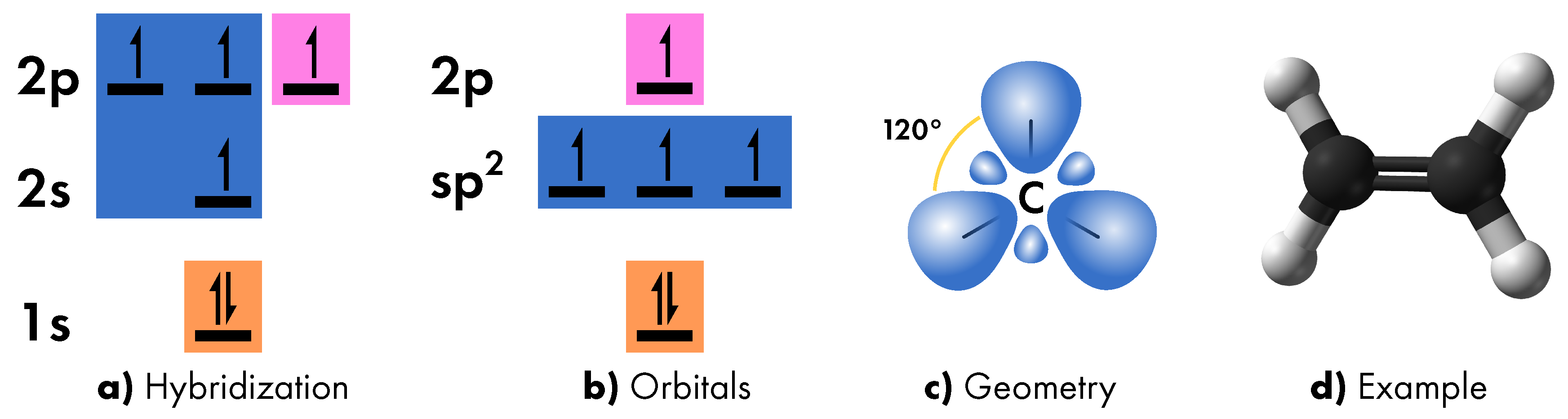
- which involves the 2s orbital and two 2p orbitals (Figure 4a). As in the previous case, the three hybrid orbitals are placed at intermediate energy (Figure 4b), are characterized by asymmetric lobes (due to the 2p contribution), but are now arranged along three different axes, thus assuming a planar triangular geometry (Figure 4c). In the formation of molecular bonds, the sp2 orbitals contribute to the formation of a double bond together with the only remaining 2p orbital, as in ethene molecule. In this case, the two carbon atoms share one electron of one sp2 orbital so as to form a σ bond and the electron of the remaining 2p orbital for the formation of a π bond (Figure 4d). A notable case is benzene molecule whereby three π bonds give rise to a delocalized orbital all around the carbon hexagon. Such a feature is relevant for electron transport in carbon systems.
- sp3 hybridization
- which involves the 2s orbital and all the 2p orbitals (Figure 5a). As in the previous case, the three hybrid orbitals are placed at intermediate energy (Figure 5b), are characterized by asymmetric lobes (due to the 2p contribution), but are now arranged along four different axes, thus assuming a tetrahedral geometry (Figure 5c). In the formation of molecular bonds, the sp3 orbitals contribute to the formation of single bonds, as in ethane molecule. In this case, the two carbon atoms share only the electron of one sp3 orbital to form a σ bond (Figure 5d).
Allotropes of Carbon
Between the discussed hybridization schemes, only sp2 and sp3 contribute to the various structures of carbon materials. Nevertheless, the chance to assume two possible bond schemes is sufficient to determine the presence of carbon allotropes. In this section, the macroscopic allotropes of carbon are briefly discussed, as case study of carbon and introduction to the more various case of nanomaterials is given emphasizing, in particular, the role of carbon orbital hybridization in the definition of the various structures. The two main forms assumed by carbon in the macroscopic scale are the well-known diamond, and graphite [28,29], both depicted in Figure 6. Diamond is composed by carbon atoms featuring sp3 hybridization and, in accordance with the bond geometry for this hybridization, carbon atoms are arranged in a three-dimensional tetrahedral lattice (Figure 6a). On the other hand, graphite is composed by carbon atoms in sp2 hybridization, which are arranged in various two-dimensional hexagonal lattices. The latter stacked one upon the other by weak van der Waals interactions (Figure 6b). From this perspective, graphite is nothing more than a quasi-infinite stacking of graphene layers [2]. It is impressive that in spite of the same composition (namely only constituted by carbon), this two materials show completely opposed properties which, as a consequence, result exclusively from the different hybridization of carbon atoms, and the consequent different structure which it gives rise. Diamond has very high hardness, whereas graphite is quite fragile, due to the weak bond between the single layers of which it is made. Moreover, graphite is an electrical conductor, whereas diamond, featured by a bandgap equal to 5.5 eV is an insulator. As a consequence, diamond is transparent at the visible light, whereas graphite has a flat absorption spectrum, which makes it black.
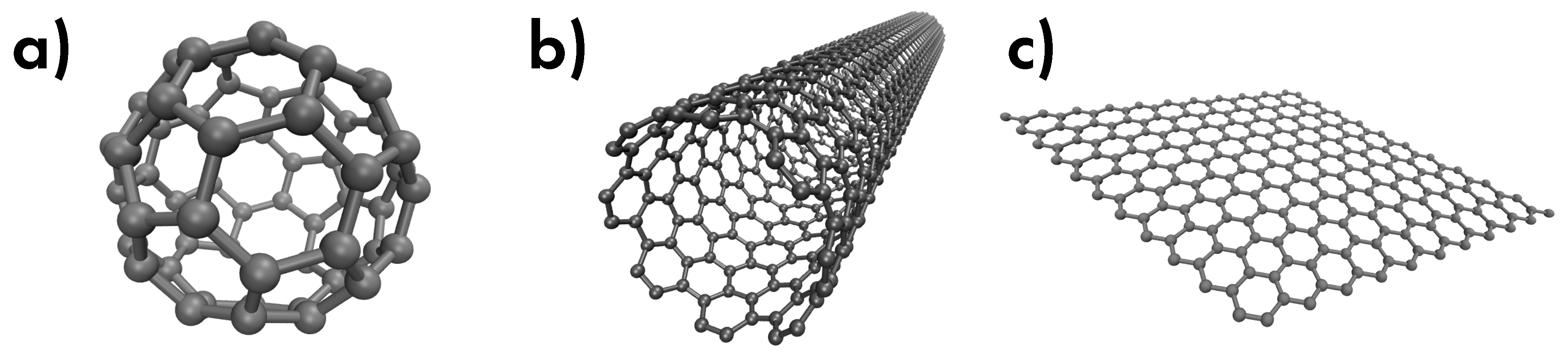
Heading down to the nanoscale world, much more carbon-based structures can be found, whose properties are related not only to the various hybridization, but also to the limitation of space dimension. As previously noticed, the main carbon-based nanomaterials are, in order of discovery, fullerene (Figure 7a), carbon nanotubes (Figure 7b), and graphene (Figure 7c). Fullerene is a 0D carbon system constituted by a single shell of carbon atoms arranged in a sphere-like surface according to an ordinate polyhedral structure. For example, for the most abundant kind of fullerene, namely C60, the atom structure corresponds to a truncated icosahedron [33]. In general, various types of fullerene are obtained on varying the mixed contribution of sp2 and sp3 hybrid orbitals, with a further amount of the first one with increasing of fullerene size [2]. In particular, by considering ever larger fullerenes, their surface approaches a planar geometry, and as their diameter approaches infinity, a perfect 2D system surface is obtained which actually corresponds to graphene.
As mentioned in the previous section, graphene is a single layer of graphite sheet, and only sp2 hybridization is featured [2]. In the case of fullerenes, the contribution of sp3 hybridization limits the delocalization of electrons on the entire surface [33]. On the contrary, the complete predominance of sp2 hybridization in graphene allows the formation of continuous delocalized molecular orbital deriving by π bonds, similar to the case of benzene previously reported [34,35]. As discussed in the following section, this feature is fundamental for the peculiar electrical behavior of graphene.
Finally, carbon nanotubes can be figured in the midway between fullerene and graphene. In this case, carbon atoms are arranged on a cylindrical surface, with length infinitely larger than the diameter [2,36]. As for fullerene, carbon nanotubes are characterized by a mixed contribution of sp2 and sp3 hybrid orbitals which determines their electronic properties ranging from semiconductor to metal [36]. On the other hand, as in the case of graphene, because of the large contribution of sp2 hybridization, delocalized orbitals can also occur, depending on the specific structure of the carbon nanotube [36]. As shown, the particular structure assumed by carbon atoms in various nanomaterials strongly affects the distribution of electron orbitals and the electrical behavior of carbon nanomaterial.
3. Electronic Structure
3.1. Energy Bands
The band structure of graphene can be derived by various methods, such as Density Functional Theory [37], pseudo-potential [38], and tight-binding method [23,26,39]. The latter method, in spite of its simplicity, provides a useful description of the contribution of π and σ orbitals in the electronic structure, and in particular in the electron transport of graphene.
A simple way to reconstruct the total wavefunction of a poly-atomic system (both for molecules and solids) is to use a Linear Combination of Atomic Orbitals (LCAO) of each single atom [30,40]. Herein, the tight-binding approximation consists of the assumption that the influence of each atom on the other is small, and therefore the atomic orbitals of free atoms can be used for their total energy determination [30,40]. In accordance with the Bloch’s theorem, the wavefunction of an electron subjected to a periodic potential (as in the case of crystals) does not depend on translations along the lattice vectors and must thereby be expressed in the form of Bloch’s function, that is as the product of a planewave of wavevector k and a lattice-periodic function [30]:
In a crystal with n atoms in its unit cell, n Bloch functions can be used as eigenstates basis and the wavefunction of the i-th atom is given by
where the summation is taken over the positions of the atom in the unit cell, for the (N ~ 1024) unit cells of the crystal, and are atomic orbitals for the i-th state. Therefore, any wavefunction can be expressed in terms of such set of functions:
where are the coefficients of vector decomposition. Given the Hamiltonian of the solid system, the solution of the Schrödinger’s equation for the wavefunction is
Herein, the i-th eigenvalue of Hamiltonian for a given is obtained by solving the secular equation
where the integrals over the Bloch’s orbitals and are called transfer integral and overlap integral matrices, respectively, and their elements are defined as
In particular, since Equation (5) is an equation of degree n, its solutions will give the n eigenvalues of energy, i.e., the energy dispersion relations (or energy bands) .
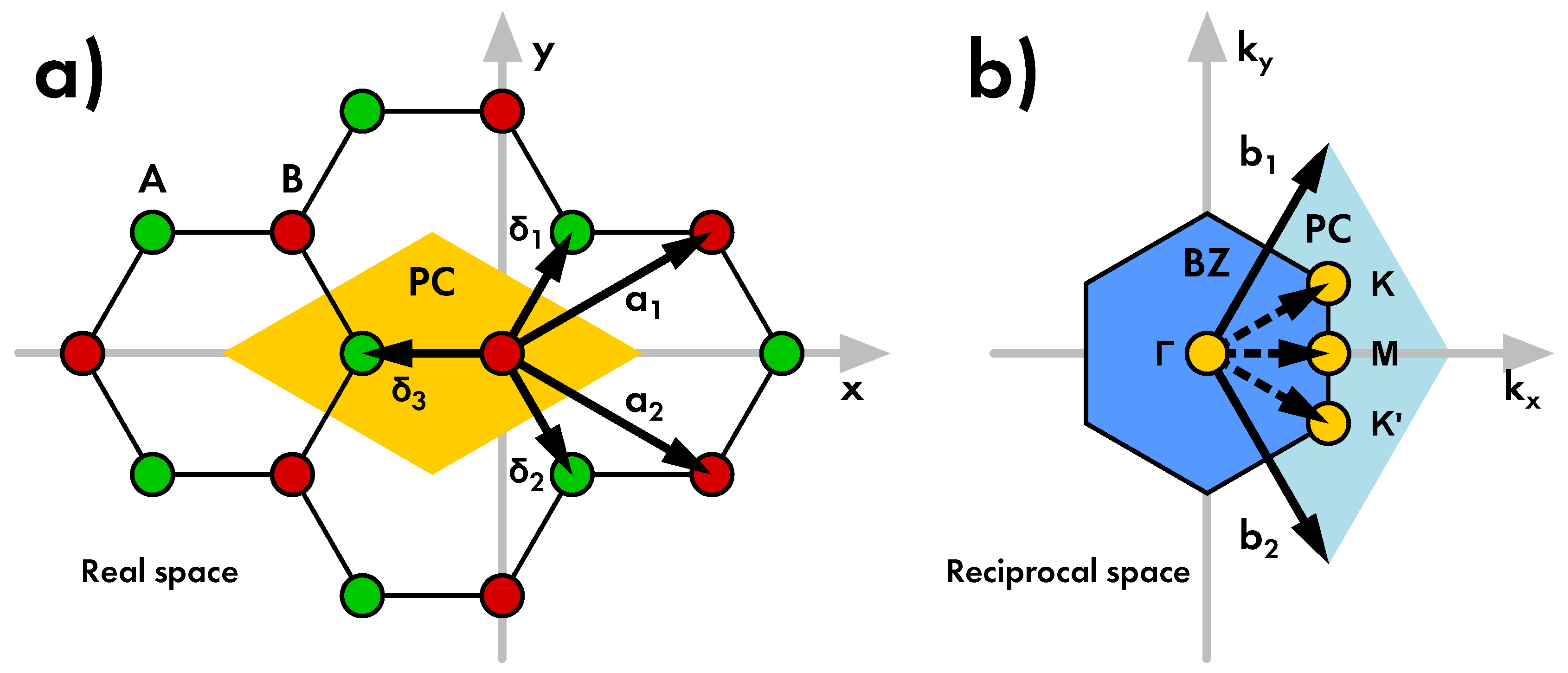
The first aspect to consider is the crystalline structure of the material to describe the electronic structure of graphene. As previously discussed, graphene is composed by carbon atoms arranged in a hexagonal structure. As shown in Figure 8, this structure is equivalent to the composition of two hexagonal Bravais lattices, marked by A and B [23,30]. The position of each carbon atom in the space can be decomposed in terms of an opportune basis as where m and n are two integers, and and are the lattice vectors defined as
in terms of their coordinates, and 1.42 Å is the lattice constant of graphene expressed in terms of the C-C bond length. These vectors also define the primitive cell of graphene lattice which, because of the composition of the two sub-lattices, includes two carbon atoms [23]. In addition, with reference to each carbon atom, the positions of first-nearest neighbors (belonging to the other sub-lattice) are given by the vectors
whereas the six second-nearest neighbors (belonging to the same sub-lattice) are placed at [23]
The vectors and describing the reciprocal lattice of graphene, defined as are then [30]
The most important region in the reciprocal space is the first Brillouin zone, since the remaining space is a periodical copy of this basic zone. In particular, notable points of Brillouin zone are the high-symmetry points , , , and , which are placed at the center of the first Brillouin zone, at its corners and at the center of its sides, respectively. These points are given in terms of coordinates by [23]
Due to the periodicity of atoms in a crystal lattice, the entire discussion of the electronic structure can be restricted to the couple of atoms included in the unit cell of graphene. Since different bands can be derived by considering the π or the σ orbitals of both carbon atoms, the Bloch’s function for electrons in the unit cell of graphene is given by:
where the summation is taken over the position for A and B carbon atoms. As discussed in Section 2, the π molecular orbital between carbon atoms of graphene is obtained by the combination of the remaining 2pz orbitals. In this case, the Equation (13) can be written as
where 2pz, , and . In accordance with the tight-binding approximation, only the contributions from terms up to nearest neighbors are considered to easily calculate the transfer and overlap matrix elements. By substituting Equation (14) in Equation (7), the diagonal elements of atom is given by:
where for the sake of simplicity, since the highest contribution arises from the same atom terms, the smaller contribution of first-nearest-neighbors is neglected. Similarly, the second diagonal term of B atom is given by . On the contrary, the highest contribution for the calculation of the off-diagonal element arises from nearest-neighbor placed at , the elements can be written as
where and the function is the sum of the phase factors. Similarly, the further off-diagonal element is given by . On the other hand, by using similar arguments, the elements of overlap matrix are given by:
where . Therefore, the secular equation takes the form
thus, obtaining the energy dispersion relation in the form
where the values for the choice of + or − sign correspond to the energy bands of π and π* molecular orbital (that is the valence and the conduction band, respectively) and the modulus of the complex function is given by
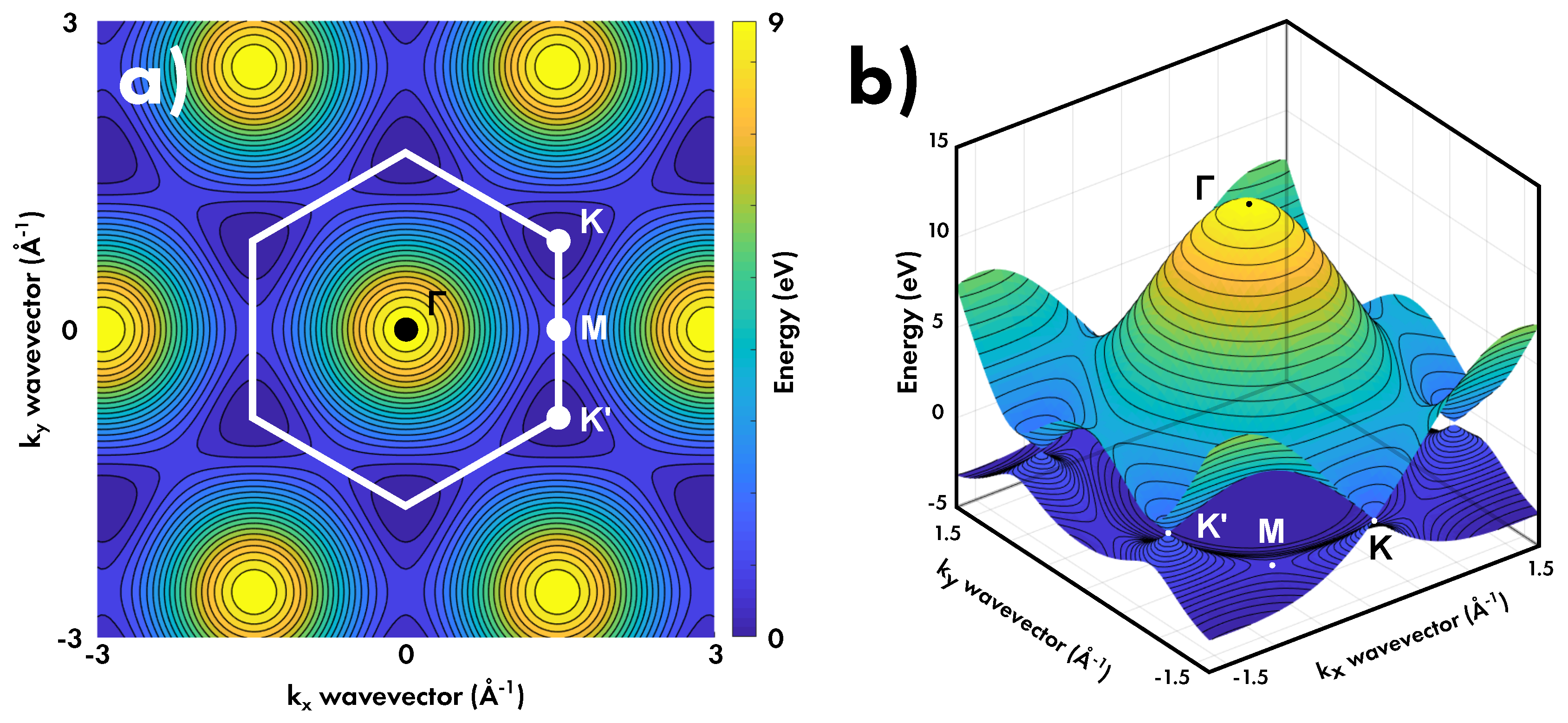
The parameters t and s are not uniquely identified, but their values are typically given in the range −(2.8–3.033) eV and 0.07–0.129 eV in order to fit theoretical or experimental data [23]. In addition, the energy for wavevector null is usually chosen null, but its experimental value corresponds to the work function of graphene with no charge doping equal to φGr = −4.6 eV [41].
A representation of the energy dispersion relations of Equation (19) is plotted in Figure 9 for finite values of t and s from Ref. [23]. Some important features of graphene energy bands can be highlighted. For 0, the conduction and the valence bands are asymmetric and thus the electron-hole symmetry is broken. As a result of the symmetry between the A and B sub-lattices (i.e., these lattices are composed by the same atomic species), the bands are not completely separated, but they are in contact at the and points of Brillouin zone. In particular, the expansion of the full band structure of Equation (19) close to the and points is isotropic, and it is given by
where 106 m/s is the Fermi velocity [23]. At the and points the dispersion relation thereby follows a linear relation, thus resembling the form of an ultrarelativistic particle described by Dirac equation for effective massless particle [23,42,43]. Therefore, the energy bands of graphene at the and points are commonly said Dirac cones. Moreover, a maximum and a saddle point are determined at the and , respectively, where in addition a bandgap of ~20 eV and ~6 eV are found. Due to this feature, graphene is a semiconductor with null bandgap, hence it falls under the category of semimetals. Finally, since the electronic density n is related to the Fermi momentum by the relation , a relation with Fermi energy can be established in the form [23]
3.2. Charge Carrier Density
The dispersion relation obtained in Equation (19) provides information of what energy is allowed for states of conduction or valence bands at given wave vector . However, in order to achieve a complete description of electronic behavior of graphene it is necessary to answer to the following questions [30]: (1) how many states exist for a given energy? (2) what is the probability of occupation of these states? Concerning the latter question, due to the fermionic nature of electrons, the probability that a conduction electron of graphene occupies a state at given energy is described by the Fermi-Dirac distribution given by
where is the Fermi energy of the system, is the Boltzmann constant, and T is the statistic temperature of the system [44]. This distribution is a step-like function which indicates that the occupation of energy levels placed below as even probability, whereas the occupation probability fades for energy levels placed above . The smooth of decreases for every lower T, up to assume a full step shape.
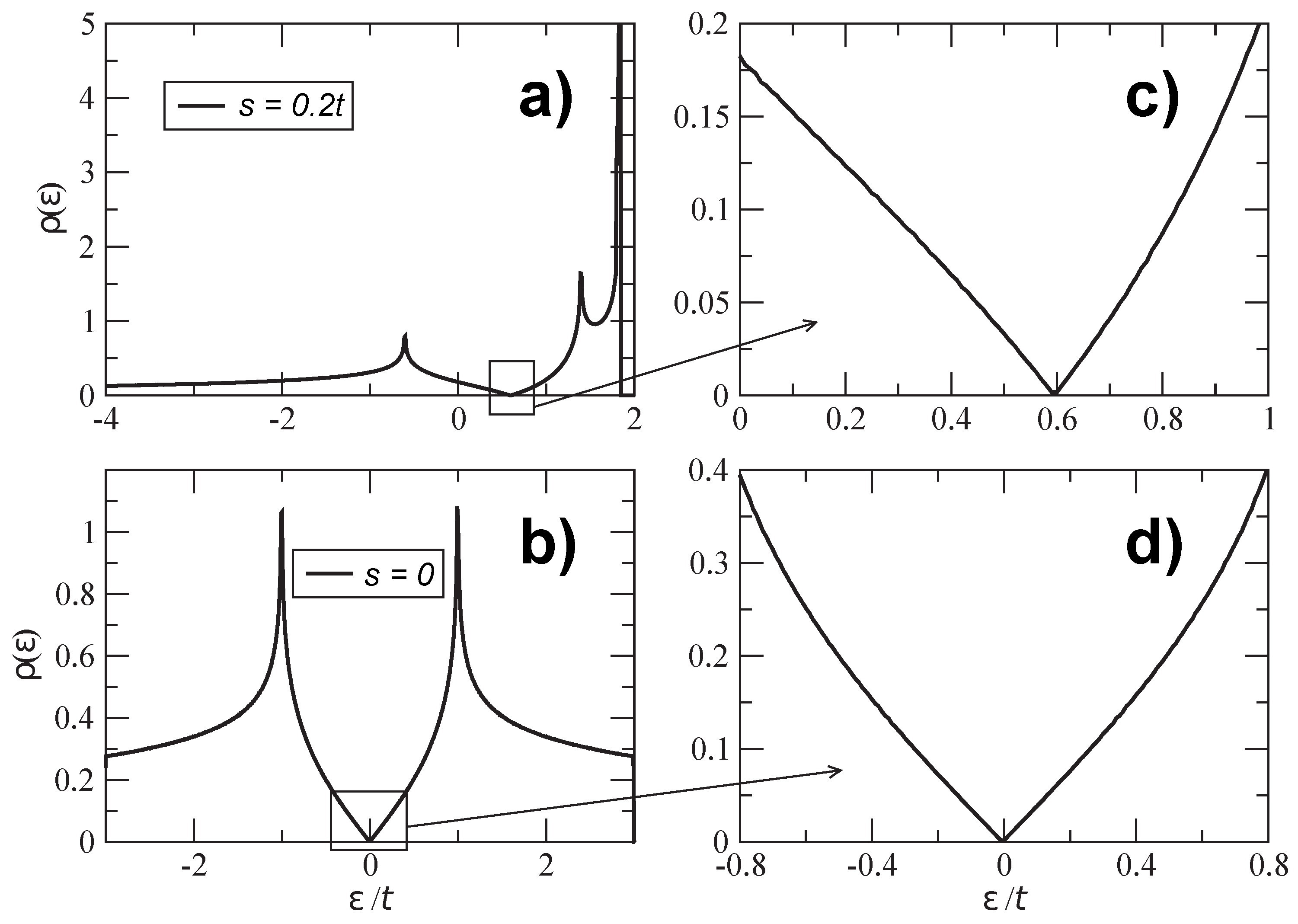
On the other hand, the way in which the states are distributed on energy, i.e., their degeneracy, is described by the density of states (DOS) [30,44]. Despite an analytic derivation of graphene DOS is possible by assuming in Equation (19), only a qualitative discussion is herein reported, by taking care to highlight the most relevant aspects concerning graphene: the derivative of dispersion relation , and the reduced dimensionality of the system. By considering the DOS at a given energy , the number of states at energy between E and is expressed by . This quantity can be obtained by integrating , i.e., the number of states with wavevector between and over the entire -space [30]
As previously noticed, the dimension of the k-space is equal to the dimension n of real space, and therefore, a hypersurface defined in this space is characterized by dimension . By labeling the electronic states by their wave vector, and by considering the possible states of a system at a given energy , a corresponding hypersurface is selected in the k-space [30,44]. The integrand of Equation (24) can be evaluated as
where the factor 2 is for the spin degeneracy, and thus Equation (24) becomes
This volume integral can be expressed as a surface integral over the isoenergy surface . In particular, the volume element can be written as . The vector is perpendicular to the surface , and proportional to the gradient of energy . Thence its differential is , and Equation (26) can be given by
In this equation, it is easy to note that for a specific value of in which , i.e., minima, maxima and saddle points of , the DOS diverges, giving rise to the so-called van Hove singularities [30]. On this basis, for a free gas of electrons of a n-dimensional system, the number of states up to energy is given by the integral
By considering the dependence on the modulus of the wave vector only, the surface element in the second member of Equation (28) is proportional to the surface of a -sphere
the DOS is thereby obtained through the derivative of the solution of Equation (28) for the various volume elements of Equation (29). In general, the dependencies on energy obtained for are given by
and therefore, no general dependence of DOS on energy should be guessed for 2D systems, as for example electrons in graphene. On the basis of these arguments, it is possible to comment the DOS of graphene reported in Figure 10. Since the 2D nature of the system no general trend on energy is determined. However, two van Hove singularities are determined by the saddle point for at the point (Figure 9). As mentioned in the discussion of the energy bands, the symmetry between electrons and holes is broken for . Such an aspect involves the DOS too, where the DOS for holes is enhanced by the symmetry break. Finally, for ideal graphene the DOS vanishes for , whereas for doped graphene non-null contributions can be introduced [45].
4. Optical Properties
Once the electronic properties of graphene are known, it is possible to correctly interpret the optical features of graphene, i.e., the interaction of graphene with photons. Therefore, such a knowledge allows the relating of the information obtained by various spectroscopies to the electronic structure of graphene. In this section, the optical absorption and the light emission of graphene are briefly described.
4.1. Light Absorption
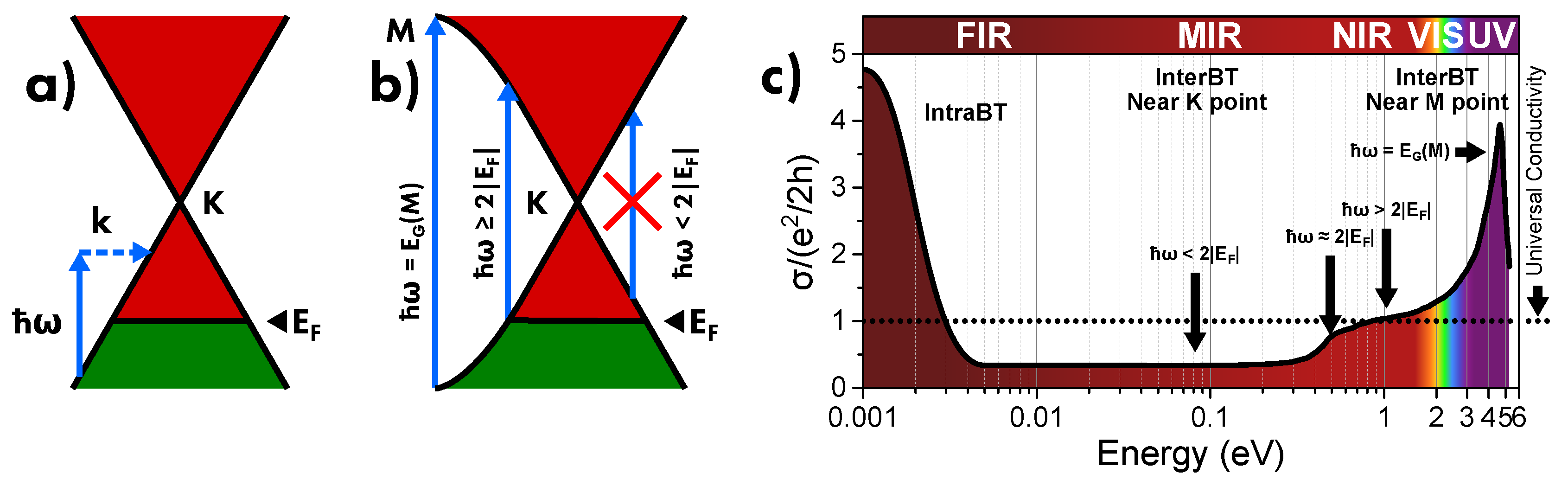
Because of the zero bandgap between valence and conduction bands, graphene absorbs light in a wide range of the electromagnetic spectrum, i.e., in far-infrared (FIR), mid-infrared (MIR), near-infrared (NIR), visible, and ultravioled (UV) region, as illustrated in Figure 11 [22]. For undoped graphene, the theoretical optical conductivity for electrons is found to be independent of frequency and equal to
where e is the electron charge, and h is the Planck’s constant, and the optical absorbance is thereby given by
where c is the speed of light, i.e., proportional to the fine structure constant , and equal to the 2.3% of incident light [46,47]. It is impressive that the effect is caused by a single layer of carbon atoms, but since almost all of the light is transmitted, graphene is a good candidate to be used as transparent conductive layer [3]. However, two critical factors restrict the simple white absorption is to the NIR-visible region: the Fermi level determined by doping (by which graphene is actually almost always affected, even if unintentionally) and the singularities in DOS [3,22,47]. Due to the large bandgap at the point of the first Brillouin zone, the optical phenomena of graphene are related to electron placed near the and the points, depending on the amount of energy involved. In particular, at low energy, intraband transitions are activated, whereas interband transitions arise at higher energy [22,48].
In the FIR region, the optical absorption of graphene is due to intraband indirect transitions, whose diagram is shown in Figure 11a. In this case, both the start and the final electronic states are placed in the valence band, and a phonons or defect-assisted scattering of electrons is required to satisfy the momentum conservation. These transitions occur both for free carriers and collective charge carriers (plasmons) [22]. In this case, concerning free carriers, the optical response is described by sheet conductivity obtained in the Drude model:
where is the conductivity and is the electron scattering time. From this quantity the Drude weight is derived, the latter corresponding to the integrated oscillator strenth of free carrier absorption. For the massless electrons of graphene, the Drude weight is given by , thus relating the intensity of optical absorption to the charge carrier density n [22]. Concerning plasmons, optical absorption is favored by the low effective electron mass and by the high doping levels attainable in graphene. In this case, an absorption band is found at a specific plasmonic resonance frequency 102 cm−1, which value can be tuned by the charge carrier density according to a proportionality relation given by [22,49].
On the other hand, the optical absorption from MIR and NIR region is related to interband transitions (shown in Figure 11b) in which the electrons are promoted by the valence band to the conduction band [22]. Contrary to the previous case, also direct transitions are allowed, and the specific weight of direct and indirect transitions depends on light energy: direct processes dominate low energy transitions ( 0.1–2 eV), whereas indirect processes prevail in the case of high energy transition ( 3 eV) [50]. As in the case of intraband transitions, the features of interband transitions are closely dependent on charge doping of graphene. In fact, as suggested by the diagram shown in Figure 11b, the lack of electrons in valence band due to p-doping induces Pauli blocking of optical transition at energy lower than [22,48,51], and hence the optical absorption of graphene can be tuned by doping. For graphene with chemical potential close to its Fermi energy, the sheet conductivity is given by
where T is the temperature and is the Boltzmann constant, characterized by a step-trend smoothed by temperature [22]. Therefore, as shown in Figure 11c, the increase of charge doping induces the formation of an absorption edge, below which no absorption is found, and therefore, as effect of oscillator-strenght sum rule, the absorbing oscillators lost in the MIR region are transferred to the low energy oscillators in the FIR region [52]. Further specific examples of doping-dependent interband transitions in graphene will be discussed in the following sections.
Finally, in the visible-NUV region, the absorption spectrum of graphene significantly deviates by the universal value πα, by featuring a broad asymmetric band at about 4.62 eV (Figure 11c) [22]. Such a feature is determined by transitions near the point, i.e., the saddle point of the Brillouin zone, where DOS features a logarithmical divergence proportional to . In addition, a many-body effect—that is electron-electron or electron-hole interactions—is involved in this process, thus determining the asymmetry of the considered band [22].
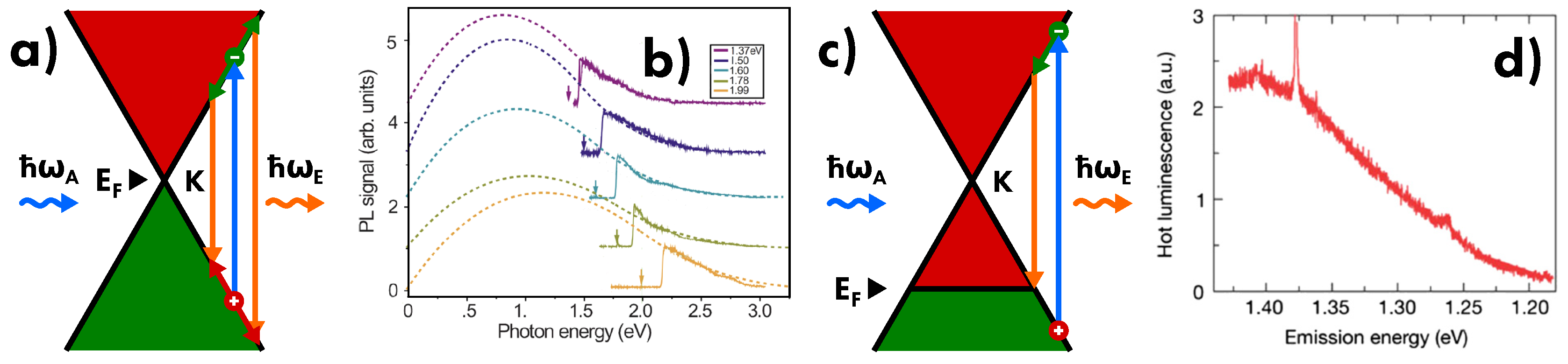
4.2. Light Emission
Since the lack of bandgap into the band structure of pristine graphene, the photocycle started from the electron-hole pairs generation by light absorption usually ends in non-radiative recombination [22]. In fact, as illustrated in Figure 12a, the electron-hole pairs generated by interband transition thermalize by rapidly relaxing towards low energy states. In particular, during the relaxation path, electron and holes differentiate their momenta, and hence the radiative recombination is prevented by the lack of momentum conservation. Therefore, the photoluminescence of graphene cannot be revealed in steady state condictions, but only by means of ultrafast spectroscopy. The emission of thermalized electron-hole pairs features a wide emission profile (Figure 12b), and decays in various time scales: fast 5–20 fs decay for direct recombination, and slow 100–250 fs and 1 ps decay for phonon assisted recombination [50]. Concerning doped graphene, the probability of radiative recombination of non-thermalized electron-hole pairs is dramatically enhanced. In fact, considering an electron-hole pair excited at energy , once electron relaxes at energy lower than , it will easily find a hole with equal momentum wherewith recombine, as depicted in Figure 12c. The emission spectrum of doped graphene is shown in Figure 12d, whose emission peak, placed at , is tuned by doping level.
5. Vibrational Properties
The modification of any graphene properties (obviously structural, but also electronic) is reflected in some deviation from the ideal lattice, and it follows that even the vibrations of lattice change. Therefore, many investigations of graphene cannot prescind using some vibrational spectroscopy. As discussed in the previous section, the information provided by IR spectroscopy is mainly related to intraband or interband electronic transitions. For such a reason, Raman spectroscopy is almost exclusively used to investigate vibrational properties of graphene.
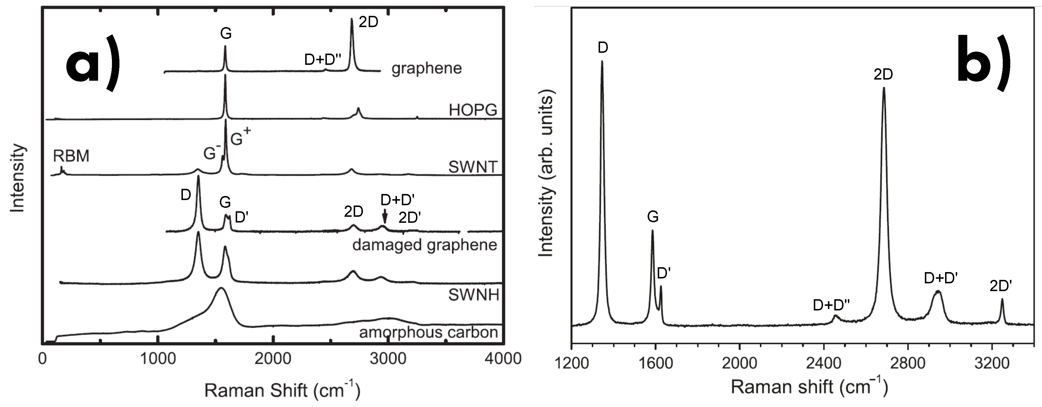
Raman spectroscopy has emerged as one of the most powerful methods in the investigation of graphene. In the one hand, Raman spectroscopy is an easy technique, is practicable at relatively low costs, with no invasiveness, and in various experimental conditions. On the other hand, despite its simple structure, graphene features a very rich Raman spectrum, composed by several well-defined bands. As shown in Figure 13, many bands of graphene are shared with other carbon-based materials, and it is easy to note how the resulting Raman spectra are sensitive to different structure. Concerning graphene, the main Raman bands which are related to one-phonon scattering processes are labeled as G (~1580 cm−1), and the defect-assisted D (~1350 cm−1), and D’ (~1620 cm−1). These bands are accompanied by those related to the respective two-phonons processes, 2D (~2680 cm−1), 2D’ (~3250 cm−1) and some composite bands, D+D’ (~1580 cm−1), and D+D’’ (~2450 cm−1). Thanks to the richness and clarity of the Raman spectrum of graphene, it is possible to use it as fingerprint, and a lot of information can be extracted by whatever anomaly in the band position or intensity [53,54].
In this section, the vibrational properties of graphene are reported regarding the normal modes and the phonon dispersion which belong to its lattice. These elements will be progressively related to the Raman active modes and to the Raman scattering processes which cause the typical spectrum of graphene.
5.1. Normal Modes and Phonon Dispersion
The symmetry of a crystalline lattice is at the basis of vibrational properties of the latter. In fact, the symmetry is involved in the definition of the fundamental vibrational features, such as phonon dispersion and normal modes. Concerning the latter, they determine every possible vibrations of the lattice. The honeycomb lattice of graphene discussed in Section 3.1 is characterized by a symmetry which belongs to the space group P6/mmm. The quantized vibrations of graphene, i.e., the phonons, are labeled by their wavevector (, with modulus q). The latter cannot assume arbitrary values, but is limited to values belonging to the first Brillouine zone of the reciprocal lattice shown in Figure 8.
The energy, and thus the frequency of phonons in graphene can be given by a force constant model, by means of which, in all similar to the case of electrons discussed in Section 3.1, the dispersion relation between frequency and wavevector and a DOS are obtained [53]. The calculated branches are shown in Figure 14a, and labeled in accordance to the kind of motion to which the atoms are subjected. In order of decreasing energy, the branches are distinguished as: three optical (O) and three acoustic (A) by involving or not a variation in charge momentum. Among them, one longitudinal (L) and two transverse (T) are distinguished according to whether the atom motion occurs along or perpendicular to the direction of the wavevector. In addition, for transverse branches only, in-plane (i) or out-of-plane (o) are distinguished according to whether the atom motion is in or out of the plane of graphene [53]. A key feature is shown by iTO and LO phonon branches where the so-called Kohn anomaly can be observed, i.e., the presence of cusps at the and points (Figure 14a).
Such a feature is typically found in metals, due to the relevant electron-phonon coupling, and is thereby a sign of the semimetallic nature of graphene. In particular, the motion of nuclei in metals is screened by the electrons, which can be described as a dielectric medium. It is shown that the derivative of phonons frequency is related to the derivative of this dielectric function. As a consequence, any singularity in the dielectric function is reflected to the phonon dispersion. The singularity and thereby the Kohn anomaly may occur for , where and are both on the Fermi surface. In graphene, the Fermi level is at , and since , two Kohn anomalies occur, for and . Finally, the weight of various branches is indicated by the phonon DOS shown in Figure 14b, thus allowing the assignment of phonon branches to spectroscopic bands [53]. The most relevant vibrational contributions come from phonons near the and points. The atom displacement of these modes in graphene is illustrated in Figure 15. At the point (), the wavevector features a symmetry belonging to the point group D6h, to which six normal modes correspond: A2u, B2g, E1u, and E2g, with double degeneration for the last two modes. Between them, only the two E2g modes are Raman active modes (Figure 15a). Moreover, at the point (), the wavevector features a symmetry belonging to the point group D3h, to which six normal modes correspond: A’1, A’2, E’, and E” with double degeneration for the last two modes (Figure 15b). In this case, all these modes are Raman active, albeit they feature different intensity [54].
Based on this information, it is possible to assign the Raman bands of graphene to specific phonon branches and atom displacements. Concerning phonons near the point, G band corresponds to the two degenerate E2g modes for phonons in iTO branch. By removing this degeneracy, G band is split in two bands, namely G+ and G–, as in the case of carbon nanotubes or strained graphene. Moreover, D’, 2D’ bands correspond to the two E2g modes for phonons in LO branch. Concerning phonons near the point, D and 2D band correspond to the A’1 mode for phonons in iTO branch, whereas D’’ band corresponds to the mode E’ in LA branch. Finally, other minor Raman bands (rarely measurable due to their very low signal intensity) D3, D4, and D5 correspond to the modes E”, E’, and A’2 for phonons in oTA, LA, and iTA branches, respectively [54].
5.2. Raman Scattering Processes
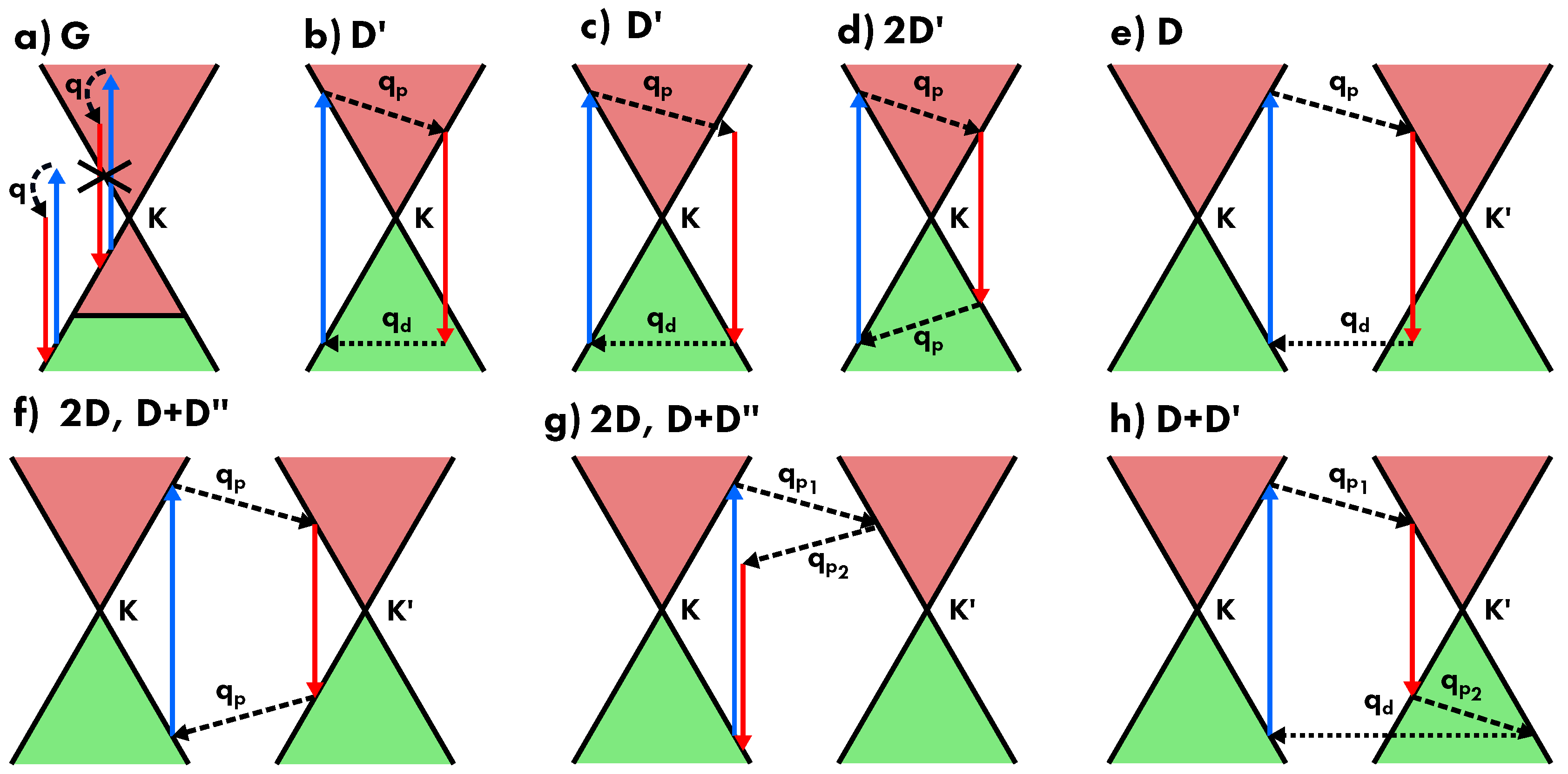
Numerous types of Raman scattering processes occur in graphene. Graphene features both resonant and non-resonant scattering, as well as one-phonon, two-phonon, and defect-assisted scattering. In addition, intravalley or intervalley scattering occur whether the light-generated electron-hole pair is scattered by a low-wavevector (low-q, for ) or high-wavevector (high-q, for ), and thus involving electronic states in a single or two Dirac cones, respectively. As illustrated in Figure 16, the main Raman bands of graphene originate from the following processes [58]:
- G band:
- belongs to a single-phonon process, in which a non-resonant electron-hole pair is scattered by a low-wavevector phonon in iTO branch corresponding to the two E2g vibrational modes (Figure 16a).
- D’ band:
- belongs to an intravalley defect-assisted single-phonon process, in which a resonant electron-hole pair is scattered by a low-q phonon in LO branch corresponding to the two E’ vibrational modes and by a defect (Figure 16b,c).
- 2D’ band:
- intravalley two-phonon process, in which a resonant electron-hole pair is scattered by two equal low-q phonons in LO branch corresponding to the two E’ vibrational modes (Figure 16d).
- D band:
- intervalley defect-assisted one-phonon process, in which a resonant electron-hole pair is scattered by a high-q phonon in iTO branch corresponding to the A’1 vibrational mode and by a defect (Figure 16e).
- 2D band:
- intervalley two-phonon process, in which a resonant electron-hole pair is scattered by two equal high-q phonons in iTO branch corresponding to the A’1 vibrational mode (Figure 16f,g).
- D+D’ band:
- intervalley defect-assisted two-phonon process, in which a resonant electron-hole pair is scattered by two different wavevector phonons, the one at low-q in iTO branch corresponding to the two E’ vibrational modes and the other at high-q in LO branch corresponding to the A’1 vibrational mode, and by a defect (Figure 16h).
- D+D’’ band:
- intervalley defect-assisted two-phonon process, in which a resonant electron-hole pair is scattered by two different wavevector phonons both at high-q value, the one in iTO corresponding to the two E’ vibrational modes and the other in LA branch corresponding to the E’ vibrational mode (Figure 16f,g).
Only a small portion of possible Raman processes are reported in Figure 16. For example, in the case of D’ mode, two scattering processes can occur as shown in Figure 16b,c, where the two processes differ only in whether scattering (phonon or defect) is in resonance with the electronic states, respectively. This aspect occurs for all the defect-assisted scattering processes above reported. Moreover, the intervalley processes are distinguished in outer (not shown) and inner (Figure 16f for 2D mode) depending on the crossing or not of Dirac cones [53,58].
6. Influencing Factors on Raman Scattering
The specific features of the reported Raman bands are closely dependent on various factors, under whose influence the appearance of Raman spectrum of graphene can vary significantly. Therefore, the monitoring of the Raman spectrum is an important way to obtain information about several properties of graphene, both of morphological and electronic nature. Herein, the most influencing factors are discussed.
6.1. Laser Energy and Power
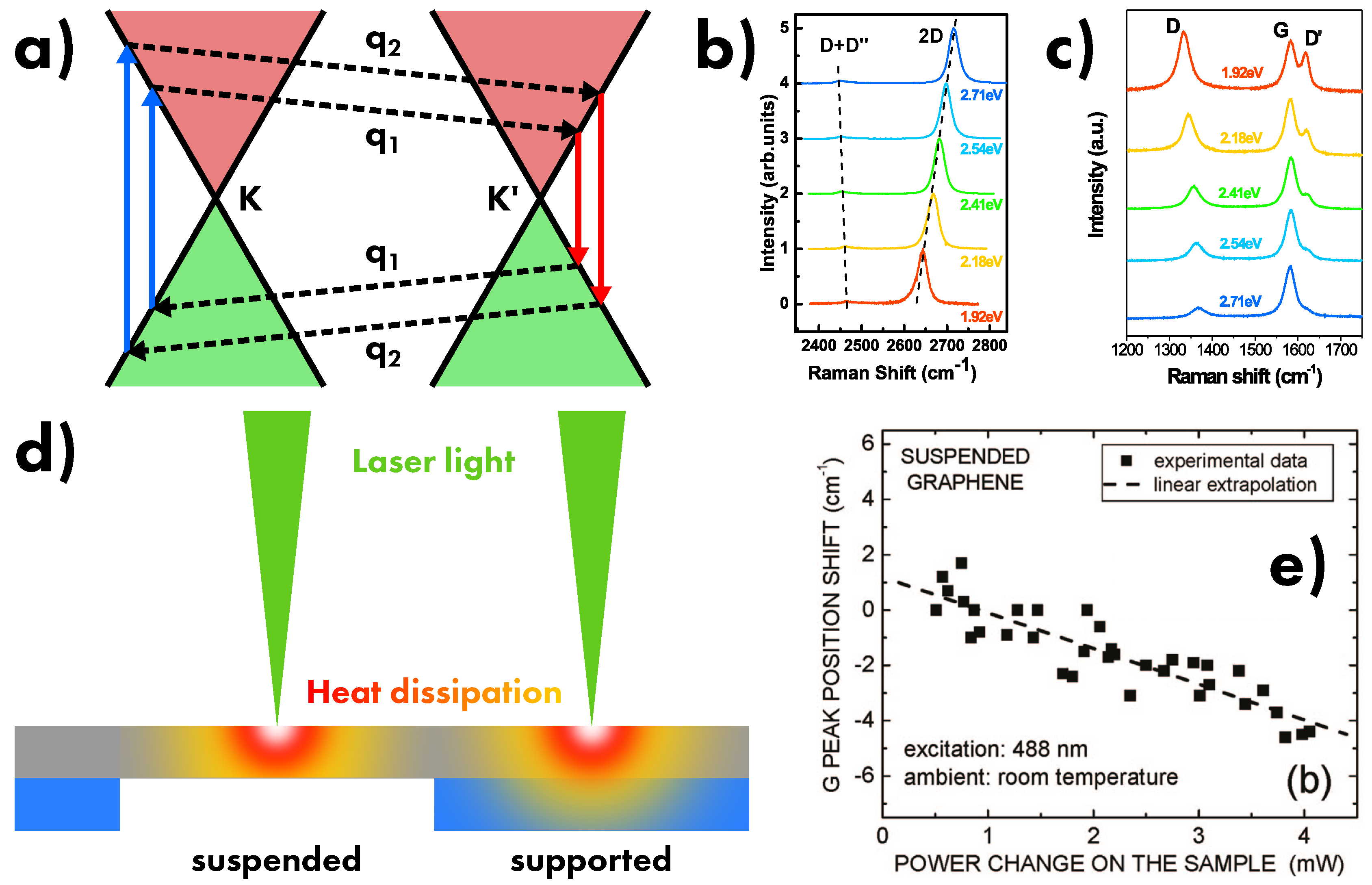
The first influence on the Raman spectrum of graphene to be considered is the dependence of G and 2D peak positions on the features of light used to induce Raman scattering (usually laser sources). Concerning the dependence on the energy, every Raman bands of graphene, except G band, feature a dispersion of its peak position on using different excitation laser energies, as well as a significant dependence of band intensity [59,60]. Such a feature can be explained by taking into account the resonant nature of the scattering processes related to these bands [42,58]. As illustrated in Figure 17, the variation of laser energy modulates the resonance with the electronic bands of graphene occurring in the scattering processes. For higher energy, the electron-hole pair at further away from the point is generated, and hence a different wavevector is necessary for the resonant scattering process. In accordance with the phonon dispersion relation shown in Figure 14, an higher mode frequency is expected. Near the point, both the electron and phonon dispersion relations can be approximated by the linear relations and , respectively, where and . By the scheme reported in Figure 17a it is shown that the laser energy can be expressed as, , whereas the energy of a single phonon is equal to , and the wavevector of the scattered phonon is given by [53]. Therefore, for 2D band, in which two phonon scatterings occur, the energy is given by
and thereby featuring a linear dispersion with the laser energy reported in Figure 17b. Finally, be νL the laser frequency, the intensity of G band is proportional to νL4, as usual for Raman scattering. On the contrary, since all the other bands arise from a resonant process, their intensity is fixed. Therefore, the relative intensity between G band and any other band varies significantly with the laser energy, as shown in Figure 17c [53,54].
On the other hand, G and 2D peak position features a significant dispersion with respect to the power of incident light which is related to thermal effects [61,62]. In fact, the lattice bonds of graphene are softened with the increase of temperature and both G and 2D bands feature a significant redshift and a similar effect can be induced during the Raman measurement. [61,63]. According to what discussed in the previous sections, a fraction of the incident light is absorbed by graphene and then dissipated by lattice vibration. As depicted in Figure 17d, the light fraction absorbed increases with laser power thus heating graphene in a well-defined region beneath the laser spot. Consequently, the bond distance increases as effect of thermal expansion thus inducing a redshift in peak position of Raman bands (Figure 17e) [61,63]. Some authors have profitably exploited the evolution of G and 2D peak positions with respect to laser power to evaluate the thermal conductivity for both suspended and supported graphene. The highest values are obtained for suspended graphene at ambient temperature, for which the thermal conductivity reaches extremely high values: ~4840–5300 W/mK [61], ~1450–3600 W/mK [64], ~1700–3200 W/mK [65]. Moreover, the thermal conductivity decreases for higher temperature (~920–1900 W/mK [64]) and for supported graphene (~50–1020 W/mK [63]) as effect of the decrease of phonon mean free path [66].
6.2. Number of Layers
Since graphene (single-layer system) and graphite (infinite-layer system) feature a considerably different Raman spectrum, a progressive evolution of the intralayer vibrations are expected for multi-layer system with arbitrary number of graphene layers. This spectroscopic feature is due to the coupling between the single layers, which do not behave as single systems, but as a collective system. Therefore, some peculiar new bands related to the relative motion between sheets (that is interlayer vibrations) appear for multi-layer graphene.
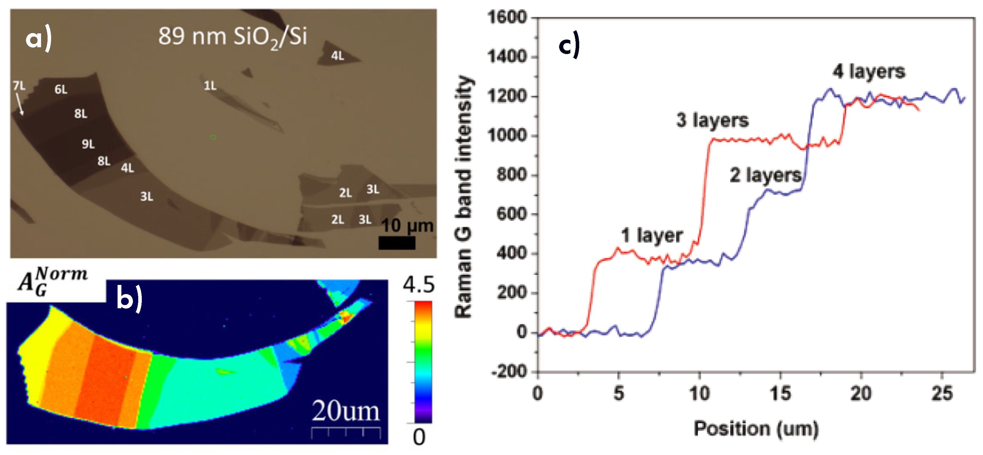
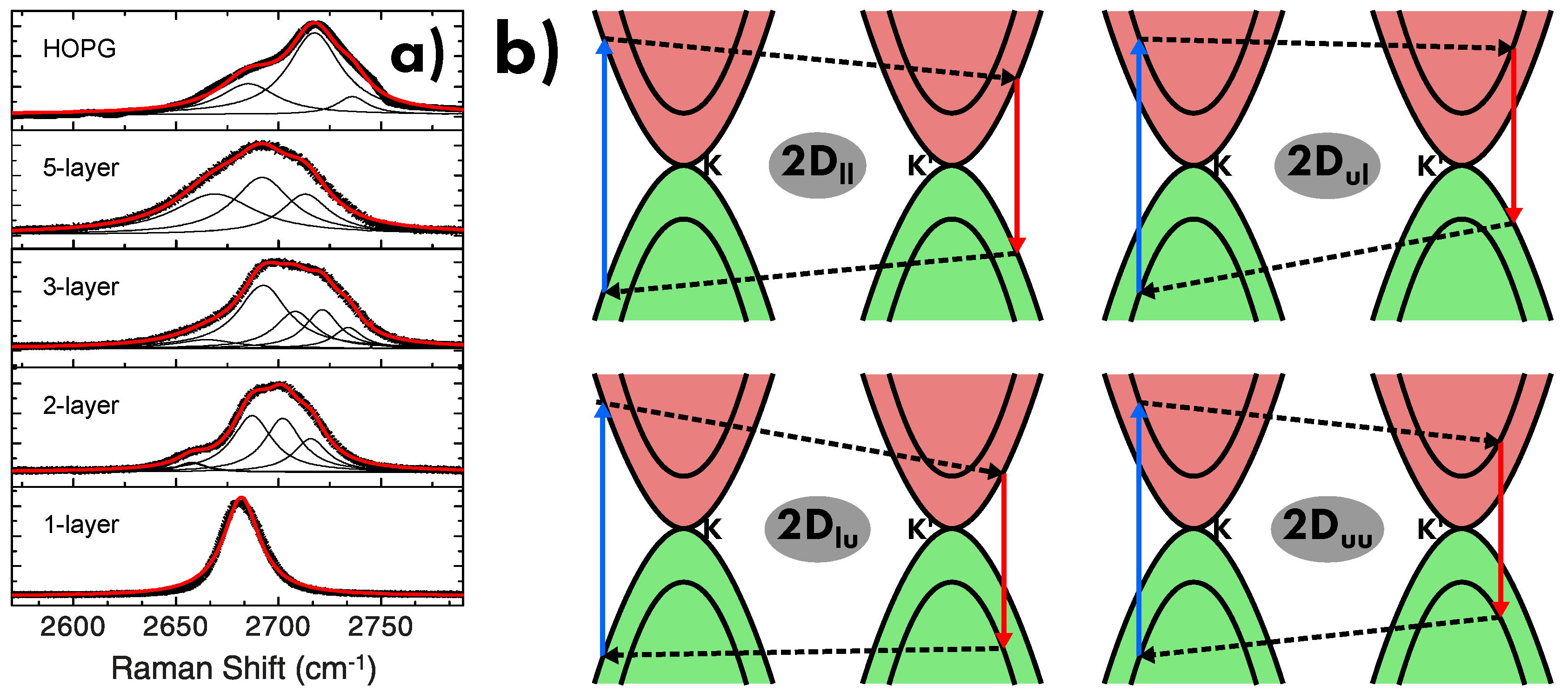
Concerning intralayer vibrations, the increasing of number of layers (demonstrated by the increase of optical contrast shown in Figure 18a), enhance the intensity of G band because of the increase of the number of scattering atoms (Figure 18b,c). Moreover, 2D band features a remarkable broadening on increasing the number of layer, thus reporting an ever large full width at half-maximum (FWHM) and an ever lower intensity ratio I2D/IG (Figure 19a) [42,67,68,69,70]. The reason of this spectroscopic evolution lies in the splitting of energy bands occurring in multi-layer graphene [42]. In particular, by considering a two-layer graphene, the vertical stacking of graphene sheets splits the conduction and the valence bands in a upper (u) and a lower (l) bands in proximity of the and points because of interlayer coupling, as illustrated in Figure 19b [42]. Therefore, the scattering process reported in Figure 16 is converted to four possible processes, hence causing the splitting of 2D band in four close subbands (2Dll, 2Dlu, 2Dul, and 2Duu), as shown in Figure 19a. For a n-layer graphene, n2 scattering processes occurs for 2D band, but their different contributions to the final shape of 2D band cannot be evaluated because of strong energy overlap. For this reason, just more than five layers are enough to get the 2D band almost indistinguishable from the case of graphite [20,21]. Therefore, by considering the simultaneous increase of G band intensity and the broadening of 2D band with the number of layers, the peak amplitude ratio between 2D and G bands (I2D/IG) is an easy parameter to rapidly evaluate the presence of a single-layer graphene. In fact, this is the only case in which I2D/IG≥ 1, whereas G band becomes dominating for every multi-layer graphene. Finally, it is important to notice that the specific stacking of graphene layer influences the splitting of electronic bands and hence the shape of 2D band [42].
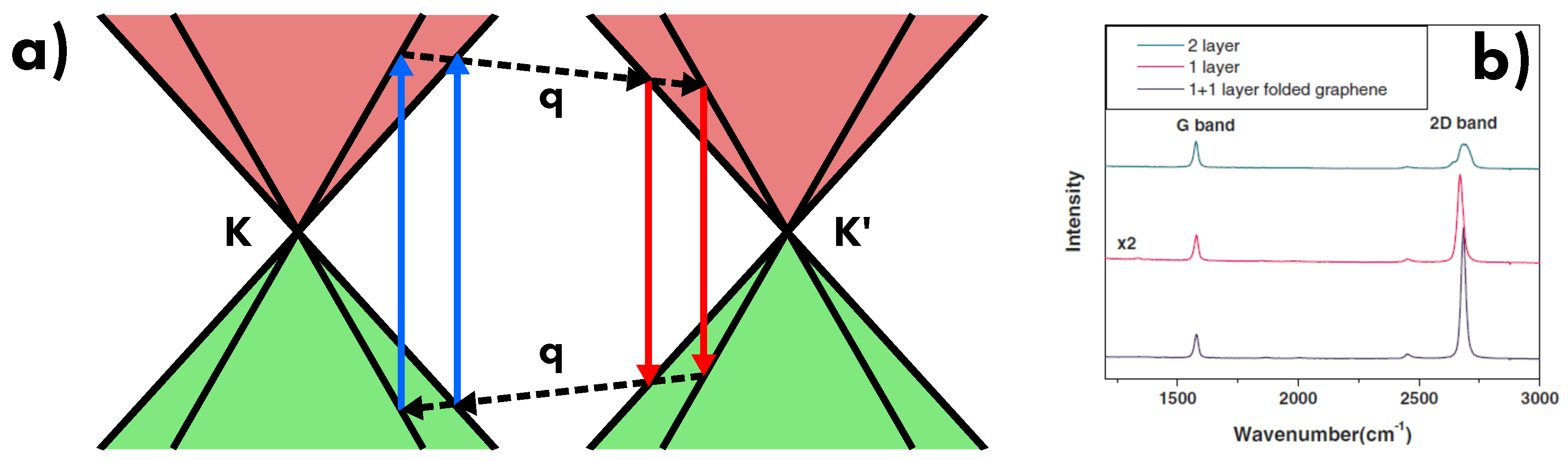
In addition, the interlayer coupling vanishes for specific alignments, thus obtaining two overlapped and independent graphene sheets. As shown in Figure 20a, folded graphene features a reduction in Fermi velocity which, according to Equation (21), modifies the slope of the electronic bands at the point, and thus phonon at higher wavevectors are necessary for the scattering cycle of 2D band [71]. The relation between Fermi energy and the 2D frequency shift is thereby given by
where is the energy of laser, and is the frequency of 2D band, which increases on decreasing the Fermi velocity (Figure 20b) [71].
Finally, concerning interlayer vibrations, the main modes which arise from the relative motion between graphene sheets are: the shear vibrational mode (C) which corresponds to a low-frequency E2g mode located between 30–44 cm−1 depending on the number of layers, and the layer-breathing modes (LBMs) located between 80–300 cm−1 [54,58].
6.3. Defects and disorder
Another factor to be considered is the lack of structural integrity, which obviously affects the vibration of a crystal lattice, and therefore, the Raman spectrum of graphene shows pronounced variation due to the presence of defects and disorder of the material.
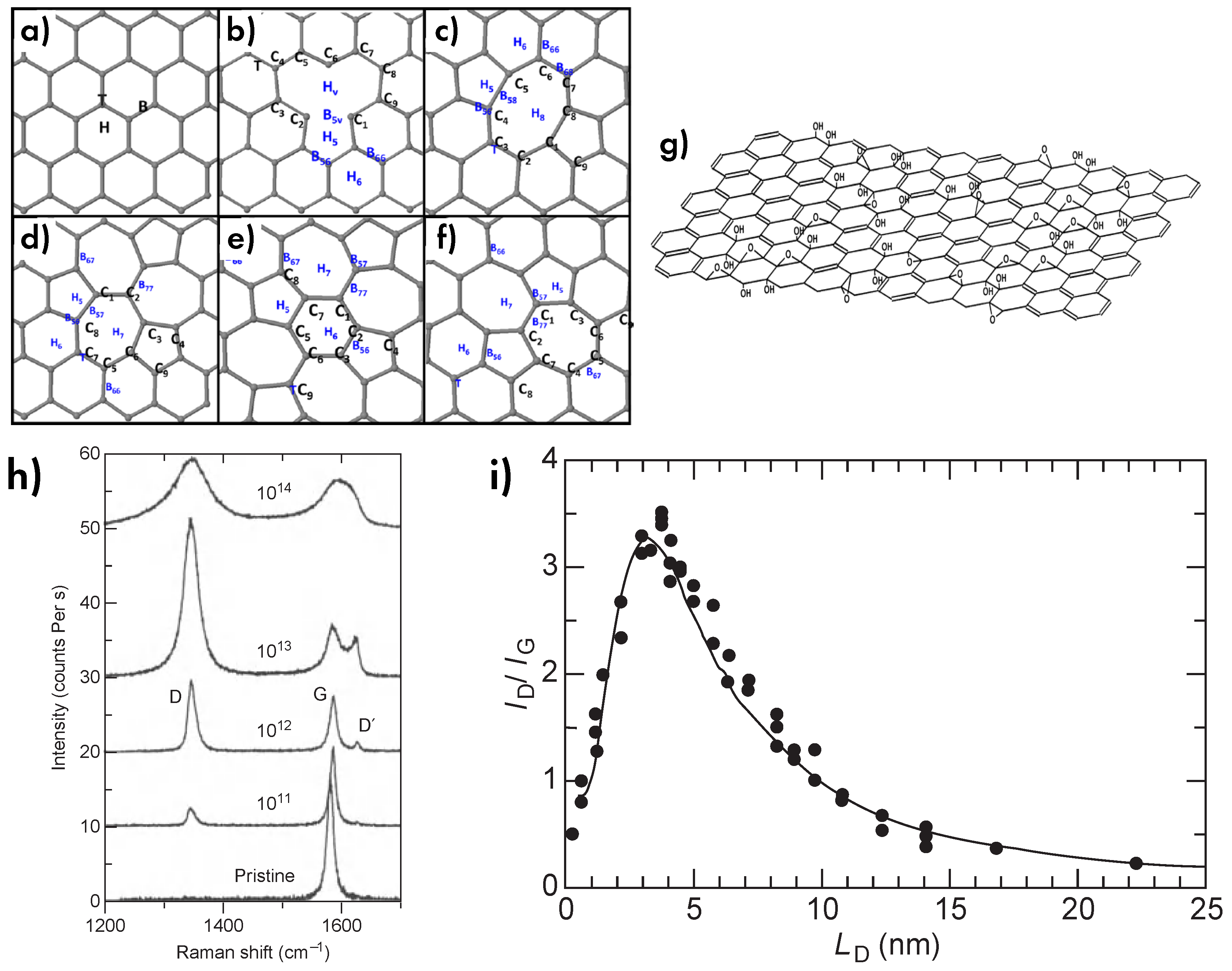
Concerning the internal region of graphene flakes, various kind of defects can affect the structure of graphene. As shown in Figure 21a–f, some of them are characterized by the lack of carbon atoms and by the consequent position rearrangement for the remaining atoms [72]. Such defects are typically related to domain-boundary region of graphene, where different crystalline seeds with arbitrary orientation are forced to realize a crystalline continuity [73,74]. In other cases, dangling bonds of a vacancy are saturated by other species. In particular, F (fluorinated graphene) and N (N-doped graphene) induced during graphene synthesis [75,76,77,78,79] and implanted metals such as , and are most notable atomic species [80,81,82,83,84]. Moreover along , and are typical moieties of graphene oxide (Figure 21g) [85].
As previously discussed, D and D’ band are the main defect-related Raman band of graphene, and their intensity varies considerably with the defect concentration [58,86,87]. In fact, as shown in Figure 21h,i, the generation of defects by ions bombardment on a pristine sample induces the appearance of D band. Moreover, it can be noticed that the increase of D band intensity reaches its maximum, and then decreases at ever higher concentration (evaluated in terms of interdefect distance ). Such a nonmonotonic behavior is related to the overlap efficiency between the defect sites. At low defect concentration, D band is active for undamaged zones in proximity of defect and ever more regions can be involved by increasing the defects. However, at high concentration, the defect starts to compete one each other, and D band is no more enhanced. Finally, at very high concentration, the defects limit the extension of D-active regions, and D band features a drastically reduced intensity and broadened bandwidth [54,86,87]. In addition, since the electron-phonon and the electron-defect scattering events are competitive, the same is true for the respective Raman bands, and thereby 2D band intensity is reduced by the increase of defects in graphene structure [88].
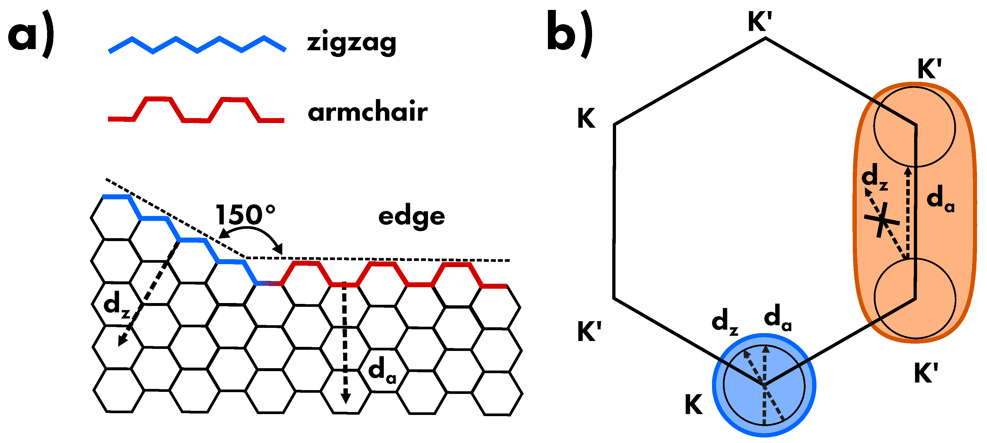
Since both D and D’ bands are the only bands which include an electron-defect scattering event, both can be used as markers of defects and disorder in graphene structure. Since these two bands are characterized by different scattering processes, their features are not a trivial duplicate. Therefore, conspicuous information about graphene structure can be obtained by comparing their spectroscopic features. As shown in Figure 14, D and D’ bands arise from phonons at different wavevector values: low value for D’, and high value for the D band. Therefore, as shown in Figure 16, D band arises from an intervalley scattering process, whereas D’ from an intravalley one. Such a feature implies a different contribution for scattering from edge defects at the border of graphene flakes. In fact, as depicted in Figure 22, when an electron collides with the edge of a flake it is scattered backward, perpendicularly to the edge interface, and thus the direction of the momentum depends on the type of graphene edge: zigzag () and armchair () [53,90,91]. As a consequence, both kinds of edge allow intravalley defect scattering which gives rise to D’ band, whereas only the armchair boundary allows the intervalley defect scattering related to D band, thus allowing determination of the edge structure on the basis of D band intensity [90,91]. Both computational and experimental investigation showed the close relation between the intensity of D’ band and the specific nature of defects [92,93], whereas the intensity of D band is mainly due to defect concentration [86,87]. Therefore, the intensity ratio ID/ID’ can be used as control parameter of defect structure. In particular, D’ band intensity increase by inducing vacancy defects, where the ID/ID’ ratio is found maximum. On the contrary the D’ band fades in the case of defect saturated by other species, thus enhancing the ID/ID’ ratio (Figure 23) [92,93].
6.4. Strain
A further morphological factor which influences the Raman spectrum of graphene is the mechanical strain to which the material can be subjected. In fact, the application of compressive or tensive strain modifies the volume of the material and thereby induces a lattice deformation: the deviation from a perfect planar geometry for compression, and the stretching of lattice for tension. Such a volume modification of graphene determines the linear dispersion of G and 2D bands shown in Figure 24 by which is easy to evaluate the structural deformation induced in the material. Most important, the Raman characterization of strain can be exploited to develop graphene-based sensor, as for example gas sensor by using graphene as impermeable membrane [94], by using graphene as strain-monitoring layer [95], and especially alongside piezoresistive effect of graphene [96,97]
By modeling the lattice bonds as a harmonic oscillator, the atom motion is described as
where M is the mass of carbon atoms, u is the atom displacement and k is the bond elastic constant characteristic for the system, and whose solution is
where A is the oscillation amplitude, and is the oscillation frequency. The strain of a material is typically described in the linear displacement regime, i.e., by applying an external force linearly proportional to the atom displacement . Therefore, the Equation (37) is rewritten as:
whose solution for is
and thereby the effect of strain is only the modification of the oscillation frequency. More generally, the equation describing the strain applied on a material can be expressed as
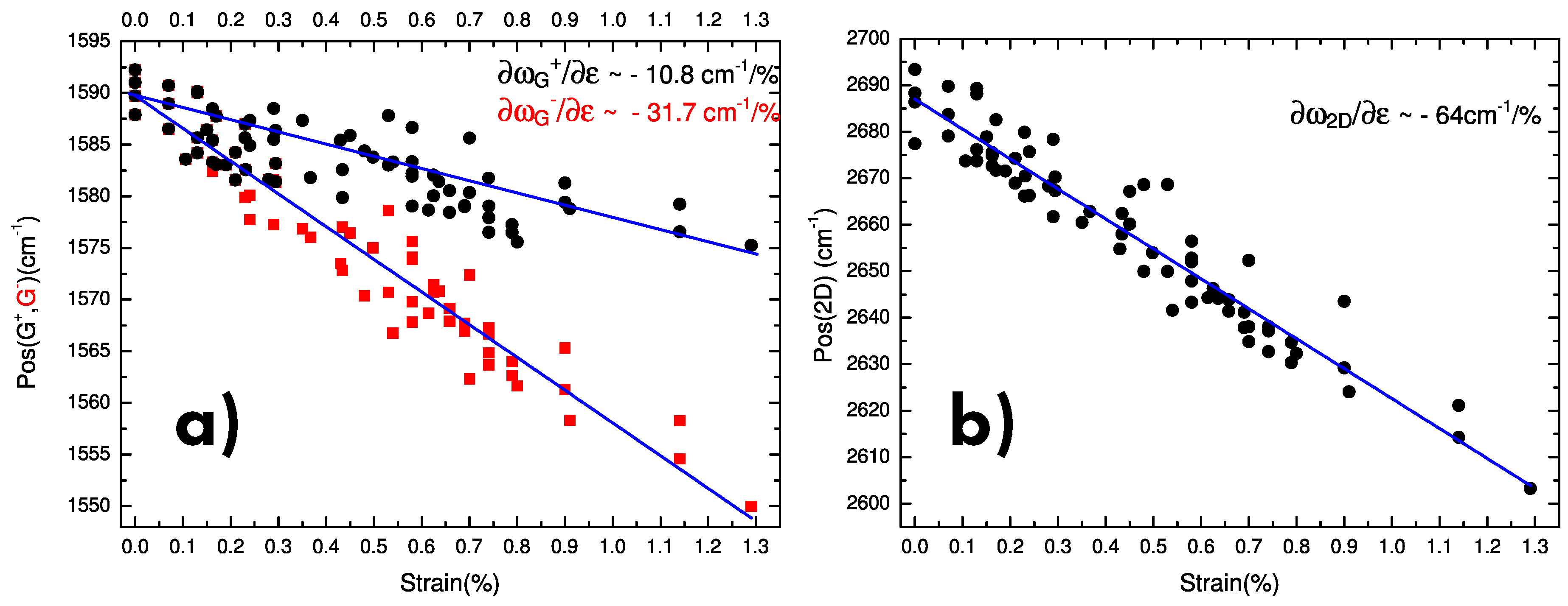
where are the elements of the second rank tensor of strain and are the elements of the fourth rank tensor which gives the change in the elastic constant element between the displacements and due to . The strain tensor in its diagonal form has the element and , which take into account the longitudinal (l) or transverse (t) orientation between strain and phonon propagating direction [53]. By considering the symmetry of the vibrational mode E2g, the solution of Equation (41) for G band (which splits in G+ and G– bands) in the case of uniaxial strain is given by
thus obtaining the dispersion of G mode by applying strain [98,99]. In Equation (42), is the mode frequency for unstrained graphene, the Grüneisen parameter describes the G frequency shift due to hydrostatic strain , and the parameter describes the G frequency shift due to shear strain [53,100]. In the case of biaxial strain , and thence Equation (42) reduces to [98]
On the other hand, by considering the symmetry of the vibrational mode A’1, the solution of Equation (41) for 2D band in the case of both uniaxial and biaxial strain is given by [98]
A linear dispersion of peak frequency by strain is thereby obtained for both G and 2D bands, in agreement with the data reported in Figure 24. However, such linear relation is largely limited to tensive strain and for compressive strain lower than 0.4%, whereas non-linear behavior starts for further compression [98,100]. Moreover, unexpected behavior is found for graphene flakes affected by domain-boundary [74].
6.5. Doping
Finally, one of the most relevant influence factors is charge doping (that is the variation in the population of electronic states of the material) especially as regards G and the 2D band features. As previously mentioned, iTO and LO phonon branches feature a strong coupling with electrons, as attested by the presence of Kohn anomaly at and points for these branches. On the basis of this coupling, the phonons and the electrons renormalize their energy as effect of a mutual interaction, which manifests itself in the phonon decay in virtual electron-hole pair (Figure 25a) [53,88]. The phonon dependence on the electron-phonon interaction can be evaluated by using second-order pertubation theory [53]. For a vibrational mode , the phonon frequency is written as
where is the unperturbed phonon frequency, and is frequency variation given by the second order perturbation term which provides the phonon frequency shift. The latter quantity and the phonon bandwidth (due to finite phonon lifetime) are given by
that is the real and imaginary parts of photon self-energy equal to
where is the matrix element for creating an electron-hole pair at momentum by means of phonon , and are the hole and electron energies, and is the decay induced bandwidth [42,53]. Therefore, both the phonon frequency and bandwidth depend on Fermi energy . The calculated curve for G phonon frequency and bandwidth on varying Fermi energy via doping concentration are shown in Figure 25b,c. By increasing doping, since the phonon cannot decay in electron-hole pair at energy lower than , its the lifetime increases and the bandwidth fades (Figure 25a). Moreover, the phonon frequency is softened for , whereas is stiffen for higher energy. For low doping, the modification of is nearly linear and symmetric under p- and n- doping. On the contrary, a high p-doping induces an ever greater stiffening, while a further softening is found for high n-doping [53,88,101,102]. This behavior is in accordance with experimental data reported in Figure 26a–c. Concerning 2D phonon, its frequency is affected by doping similarly to the case of G phonon, albeit with different ranges of linearity. In particular, the 2D frequency varies almost linearly at low doping, but softens significantly even at moderate n-doping [88,102].
Also, the integrated intensity of Raman bands are sensitive to doping. In particular, as shown in Figure 26d, whether the intensity of G band does not depend on doping, the intensity of 2D band is visibly reduced by the increase of doping, both of p- and n-type. In fact, under the assumption of a fully resonant process, the intensity of 2D band can be written as
where is the electron-phonon scattering rate, is the electron-defect scattering rate, and is the electron-electron scattering rate [88,102]. Between those terms, only depends on Fermi energy, by scaling linearly with it, and the I2D decreases on the increase of doping. Therefore, the relative intensity between G and 2D bands I2D/IG is used to monitor doping. The intrinsic value for undoped graphene has been evaluated to be I2D/IG = 12–17, but this is found only in suspended graphene, since in the case of supported graphene, the interference effects must be included [88,103,104]. Considering a typical substrate composed by about 285 nm of amorphous grown on a wafer, the interference effects reduce the value down to I2D/IG≈ 5. Moreover, lower values are typically found in experiments as effect of unintentional p-doping induced by substrate surface charges [88,105,106,107].
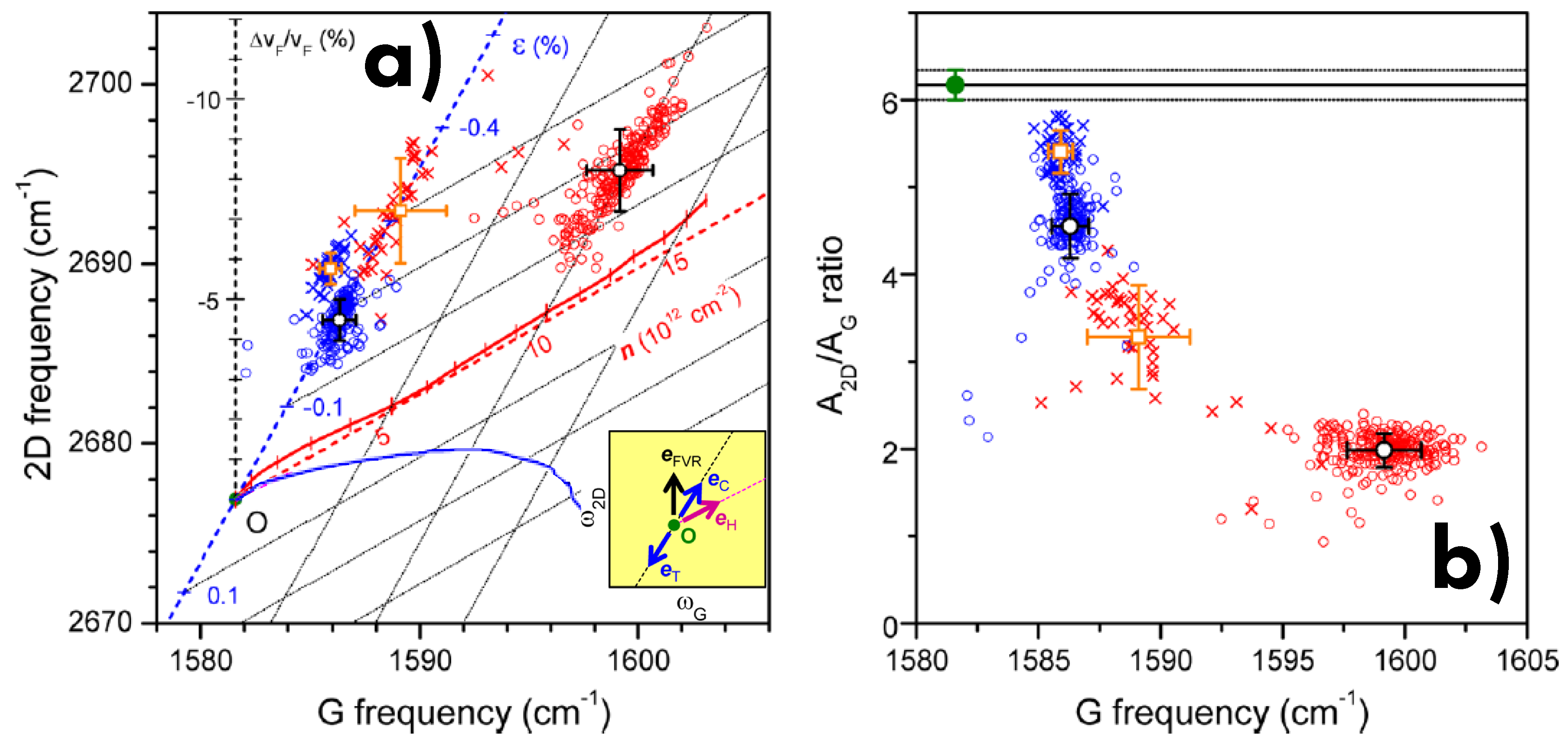
Despite the peak frequency shifts of G and 2D bands mark the actual doping in graphene samples, such an evaluation can be distorted by concurrent occurrence of other effects on these bands, such as folding or strain in graphene sheet. Nevertheless, according to the recent literature, the different contribution σ of the various effects can be partially disentangled by using a method developed by the author of Refs. [108,109,110,111,112]. Herein, the shifts of G and 2D band are analyzed by using a G-2D map obtained by plotting the peak position of 2D band vs G band (Figure 27a) calibrated according to the used laser wavelength. Here a given spectrum is represented by a single point and the contributions of doping and strain are evaluated by decomposing the position of this point against two main axes which are traced according to the single dependence on doping (different for p or n type) and strain (both tensive and compressive). The intersection between these axes corresponds to the ideal unstrained and undoped configurations. Thence, every point at the right side of strain axis can be decomposed against these axes evaluating the different contribution of doping and strain. Moreover, the points placed at the left of the strain axis require a further axis, namely the Fermi velocity axis, since neither doping nor strain can describe this region of the map.
Compared to the easy evaluation of doping obtained by I2D/IG ratio, the reported procedure gives some advantages and disadvantages (Figure 27b). In fact, I2D/IG depends only by doping and its evaluation is not affected by other phenomena. On the other hand, the G-2D map provides a more accurate evaluation of doping levels, and in some cases it allows better discrimination between p or n-doping. Nevertheless, the simultaneous occurrence of strain, doping and Fermi velocity variation cannot be disentangled. Therefore, this method requires that at least one of these parameters keep (or it is assumed to be) unmodified [108,109].
7. Synthesis Methods
Since the first isolation carried out by Novoselov and Geim in 2004 [1], a plethora of methods have been developed to produce graphene, by exploiting a wide variety of physical or chemical phenomena. Currently, the various methods show different and complementary characteristics, but none of them can comply all the possible requirements, for example large extension, large production, defect-free structure, functionalization, cleanliness from impurities, low costs. Therefore, case by case the choice between them is driven by the evaluation of which method is better suitable for the specific application in which graphene must be implemented. In general, the methods developed until now can be grouped in two categories depending on the direction of the manufacturing process: bottom up methods, which start from molecular precursor in that assembled together to build up objects of higher hierarchical level, and top down methods, in which macroscopic materials are reduced to the nano-size element of which are constituted or used as raw material, as in the case of graphite and waste plastic for graphene, respectively [18,24,25]. Some of the most common synthesis methods of graphene are described in the following.
7.1. Top Down
- Mechanical Exfoliation
- based on the separation of the single graphene sheets which constitute graphite (Figure 28a), and thanks to its simplicity this method was used for the first isolation of graphene [1]. On its favor, it produces the highest quality of graphene because of the high purity of graphite, and moreover it is a relatively easy procedure since the vertical stacking of graphene sheets is assured only by weak van der Waals interactions. For this reason this technique can be extended to other van der Waals heterostructures, such as transition metal dichalcogenide (, , , ). However, this method is limited by two main factors: the small amount of product and in the exiguous extension of graphene flakes, the latter factor bypassable by using of HOPG as raw material [42]. In detail, the direct manipulation of top graphene sheet on graphite can be performed both by scotch tape and by tips originally produced for scanning probe microscopy [24,42].
- Liquid-phase Exfoliation
- in this case the exfoliation procedure is performed in liquid-phase, and the separation of graphene sheets is obtained by sonication (Figure 28b) [24,25,42]. This procedure is preferable to the mechanical exfoliation since in comparison it produces a large quantity of graphene flakes with larger lateral size. By contrast, the most critical issue consists of the damaging of the internal structure of graphene flakes in which some defects can be induced. However, some investigations have shown that this undesired effect can be avoided by putting in solution some specific chemicals, such as surfactants [113] or intercalating molecules [114], which facilitate the exfoliation, thus requiring weaker sonication [25,42].
- Electrochemical exfoliation
- performed in liquid-phase as the previous method, but based on the use of a graphite source (usually HOPG) as electrodes in an electrolyte solution (Figure 28c). In this casethe produced graphene features low defect concentration because the sheets separation is induced by the electrochemical reaction rather than by mechanical waves, thus assuring the production of a high-quality graphene [25].
- Graphene Oxide Reduction
- uses graphene oxide (GO) as main precursor. GO is usually obtained by many methods, such as from the exfoliation of graphite oxide (Hummer’s method) which follows a top down strategy [115], or by using glucose as source (Tang-Lau method) according to a bottom up strategy [116]. Concerning the first case, the exfoliation of graphite oxide is easier than that of native graphite, thus featuring notable advantages with its respect [25]. Both chemical or thermal approaches can be exploited for the reduction of GO (Figure 28d) and the quality of graphene is determined by the degree of reduction actually reached, usually never complete [117,118]. Some authors usually name this material graphene but it should be referred as reduced graphene oxide (rGO) because of its peculiar properties. In fact, rGO significantly differs from actual graphene, and it is thereby preferred for applications which take profit from the presence of functional groups onto graphene (optical and liquid application), rather than in those in which a high purity level is mandatory (solid state microelectronic) [85,89].
7.2. Bottom Up
- Chemical Vapor Deposition (CVD)
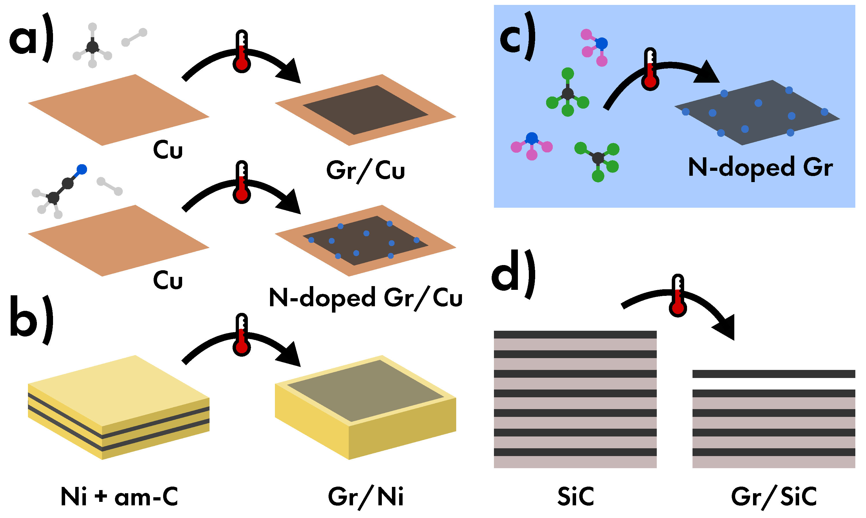
- is one of the most common methods for the production of graphene for microelectronic application both because the excellent features of the produced graphene and because it makes use of technologies well established in microelectronics industry. In particular, a mixture of molecular hydrogen and small hydrocarbon as carbon source (methane, ethane) are used to grow layer by layer the largest high-quality graphene flakes onto various substrates made by transition metals (, , , ) [8]. Moreover, by varying the precursors, it is possible to include specific dopant elements in graphene such as boron, nitrogen or oxygen in order to obtain B-doped, N-doped, or O-doped graphene (Figure 29a). Thereafter, graphene is covered by a protective layer usually made by polymers such as poly(methyl methacrylate) and then transferred onto the other substrates by using thermal release tape. Unfortunately, precisely this step constitutes the weakness of CVD methods, since some residues of the protective layer keep onto graphene even after dedicated cleaning bath [24,42,119,120]. Finally, plasma-enhanced CVD has proved an excellent method to grow vertical graphene nanosheets, i.e., a special graphene morphology which features peculiar transport properties of interest for microelectronics [121,122,123].
- Thermal Annealing
- basing on CVD method, produces graphene by using a couple or a multiple stack of an amorphous carbon layer deposited onto a metal layer (, and are the most common choices). The annealing dissolves the amorphous carbon into the metal layer, and thus obtaining the segregation of a thin carbon layer, i.e., graphene, onto the surface of the metal (Figure 29b) [24,124,125]
- Solvothermal
- in its turn similar to CVD method, produces graphene by means of the reaction between some chemicals in liquid phase (Figure 29c). Some reaction is based on the pyrolysis or the thermal decomposition of carbon-based precursors [24,126,127]. Moreover, other methods use also precursor species containing nitrogen, such as in the case of the reaction between and , thus inducing the formation of N-doped graphene flakes [124,128].
- Epitaxial Growth
- based on the synthesis of graphene by the thermal decomposition of the surface of (Figure 29d). In addition to the very high-quality structure of graphene obtained by this technique, the real advantage is the growth of graphene directly on a semiconductor. In this way it is possible to obtain the same quality of CVD, but avoiding the transfer step and the problem related to the transfer stage [25,129,130,131,132].
8. Conclusions
The present review aims to collect the knowledge regarding the structural and electronic properties of single-layer graphene, especially by pointing out the connection to the spectroscopic characteristics deriving from the electronic band structure of the material. In particular, the effects of structural changes (defects and strain) and electronic state modifications (doping) are shown through the information provided by Raman spectroscopy. Herein, we highlight the wide range of potentialities this technique in the investigation of graphene and related materials. Finally, a summary of graphene synthesis methods is reported.
Funding
This research received no external funding.
Conflicts of Interest
The authors declare no conflict of interest.
References
- Novoselov, K.S.; Geim, A.K.; Morozov, S.V.; Jiang, D.; Zhang, Y.; Dubonos, S.V.; Grigorieva, I.V.; Firsov, A.A. Electric field effect in atomically thin carbon films. Science 2004, 306, 666–669. [Google Scholar] [CrossRef] [PubMed]
- Geim, A.K.; Novoselov, K.S. The rise of graphene. Nat. Mater. 2007, 6, 183–191. [Google Scholar] [CrossRef] [PubMed]
- Bonaccorso, F.; Sun, Z.; Hasan, T.; Ferrari, A.C. Graphene photonics and optoelectronics. Nat. Photonics 2010, 4, 611. [Google Scholar] [CrossRef]
- Allen, M.J.; Tung, V.C.; Kaner, R.B. Honeycomb carbon: A review of graphene. Chem. Rev. 2009, 110, 132–145. [Google Scholar] [CrossRef]
- Randviir, E.P.; Brownson, D.A.C.; Banks, C.E. A decade of graphene research: Production, applications and outlook. Mater. Today 2014, 17, 426–432. [Google Scholar] [CrossRef]
- Kim, S.B.; Park, J.Y.; Kim, C.S.; Okuyama, K.; Lee, S.E.; Jang, H.D.; Kim, T.O. Effects of graphene in dye-sensitized solar cells based on nitrogen-doped TiO2 composite. J. Phys. Chem. C 2015, 119, 16552–16559. [Google Scholar] [CrossRef]
- Schwierz, F. Graphene transistors. Nat. Nanotechnol. 2010, 5, 487–496. [Google Scholar] [CrossRef]
- Bae, S.; Kim, H.; Lee, Y.; Xu, X.; Park, J.S.; Zheng, Y.; Balakrishnan, J.; Lei, T.; Kim, H.R.; Song, Y.I.; et al. Roll-to-roll production of 30-inch graphene films for transparent electrodes. Nat. Nanotechnol. 2010, 5, 574. [Google Scholar] [CrossRef]
- Patel, K.; Tyagi, P.K. P-type multilayer graphene as a highly efficient transparent conducting electrode in silicon heterojunction solar cells. Carbon 2017, 116, 744–752. [Google Scholar] [CrossRef]
- Giannazzo, F.; Greco, G.; Roccaforte, F.; Sonde, S. Vertical transistors based on 2D materials: Status and prospects. Crystals 2018, 8, 70. [Google Scholar] [CrossRef]
- Giannazzo, F.; Fisichella, G.; Greco, G.; La Magna, A.; Roccaforte, F.; Pécz, B.; Yakimova, R.; Dagher, R.; Michon, A.; Cordier, Y. Graphene integration with nitride semiconductors for high power and high frequency electronics. Phys. Status Solidi (A) 2017, 214, 1600460. [Google Scholar] [CrossRef]
- Zubair, A.; Nourbakhsh, A.; Hong, J.Y.; Qi, M.; Song, Y.; Jena, D.; Kong, J.; Dresselhaus, M.; Palacios, T. Hot Electron Transistor with van der Waals Base-Collector Heterojunction and High-Performance GaN Emitter. Nano Lett. 2017, 17, 3089–3096. [Google Scholar] [CrossRef] [PubMed]
- Mannequin, C.; Delamoreanu, A.; Latu-Romain, L.; Jousseaume, V.; Grampeix, H.; David, S.; Rabot, C.; Zenasni, A.; Vallee, C.; Gonon, P. Graphene-HfO2-based resistive RAM memories. Microelectron. Eng. 2016, 161, 82–86. [Google Scholar] [CrossRef]
- Fitzer, E.; Kochling, K.H.; Boehm, H.; Marsh, H. Recommended terminology for the description of carbon as a solid (IUPAC Recommendations 1995). Pure Appl. Chem. 1995, 67, 473–506. [Google Scholar] [CrossRef]
- Jeevanandam, J.; Barhoum, A.; Chan, Y.S.; Dufresne, A.; Danquah, M.K. Review on nanoparticles and nanostructured materials: History, sources, toxicity and regulations. Beilstein J. Nanotechnol. 2018, 9, 1050–1074. [Google Scholar] [CrossRef]
- Pokropivny, V.; Skorokhod, V. Classification of nanostructures by dimensionality and concept of surface forms engineering in nanomaterial science. Materi. Sci. Eng. C 2007, 27, 990–993. [Google Scholar] [CrossRef]
- Kumar, N.; Kumbhat, S. Carbon-Based Nanomaterials, 1st ed.; John Wiley & Sons: Hoboken, NJ, USA, 2016. [Google Scholar]
- Nasir, S.; Hussein, M.; Zainal, Z.; Yusof, N. Carbon-based nanomaterials/allotropes: A glimpse of their synthesis, properties and some applications. Materials 2018, 11, 295. [Google Scholar] [CrossRef]
- Roduner, E. Size matters: Why nanomaterials are different. Chem. Soc. Rev. 2006, 35, 583–592. [Google Scholar] [CrossRef]
- Dresselhaus, M.; Jorio, A.; Saito, R. Characterizing graphene, graphite, and carbon nanotubes by Raman spectroscopy. Annu. Rev. Condens. Matter Phys. 2010, 1, 89–108. [Google Scholar] [CrossRef]
- Malard, L.M.; Pimenta, M.A.A.; Dresselhaus, G.; Dresselhaus, M.S. Raman spectroscopy in graphene. Phys. Rep. 2009, 473, 51–87. [Google Scholar] [CrossRef]
- Mak, K.F.; Ju, L.; Wang, F.; Heinz, T.F. Optical spectroscopy of graphene: from the far infrared to the ultraviolet. Sol. Stat. Commun. 2012, 152, 1341–1349. [Google Scholar] [CrossRef]
- Castro Neto, A.H.; Guinea, F.; Peres, N.M.R.; Novoselov, K.S.; Geim, A.K. The electronic properties of graphene, 2009 Rev. Mod. Phys. 2009, 81, 109. [Google Scholar] [CrossRef]
- Lee, H.C.; Liu, W.W.; Chai, S.P.; Mohamed, A.R.; Aziz, A.; Khe, C.S.; Hidayah, N.M.; Hashim, U. Review of the synthesis, transfer, characterization and growth mechanisms of single and multilayer graphene. RSC Adv. 2017, 7, 15644–15693. [Google Scholar] [CrossRef]
- Coroş, M.; Pogăcean, F.; Măgeruşan, L.; Socaci, C.; Pruneanu, S. A brief overview on synthesis and applications of graphene and graphene-based nanomaterials. Front. Mater. Sci. 2019, 13, 23–32. [Google Scholar] [CrossRef]
- Saito, R.; Dresselhaus, G.; Dresselhaus, M. Physical Properties of Carbon Nanotubes; World Scientific: Singapore, 1998. [Google Scholar]
- Pace, N.R. The universal nature of biochemistry. Proc. Natl. Acad. Sci. USA 2001, 98, 805–808. [Google Scholar] [CrossRef] [PubMed] [Green Version]
- Belenkov, E.A.; Greshnyakov, V.A. Classification schemes for carbon phases and nanostructures. New Carbon Mater. 2013, 28, 273–282. [Google Scholar] [CrossRef]
- Heimann, R.; Evsyukov, S.; Koga, Y. Carbon allotropes: A suggested classification scheme based on valence orbital hybridization. Carbon 1997, 35, 1654–1658. [Google Scholar] [CrossRef]
- Grundmann, M. Physics of Semiconductors, 1st ed.; Springer International Publishing: Basel, Switzerland, 2006. [Google Scholar]
- Solomons, T.W.G.; Fryhle, C.B. Organic Chemistry, 10th ed.; John Wiley & Sons: Hoboken, NJ, USA, 2009. [Google Scholar]
- Bransden, B.H.; Joachain, C.J. Physics of Atoms and Molecules, 1st ed.; John Wiley & Sons: Hoboken, NJ, USA, 1983. [Google Scholar]
- Poater, J.; Duran, M.; Sola, M. Analysis of electronic delocalization in buckminsterfullerene (C60). Int. J. Quantum Chem. 2004, 98, 361–366. [Google Scholar] [CrossRef]
- Popov, I.A.; Bozhenko, K.V.; Boldyrev, A.I. Is graphene aromatic? Nano Res. 2012, 5, 117–123. [Google Scholar] [CrossRef]
- Kroes, J.M.H.; Fasolino, A.; Katsnelson, M.I. Density functional based simulations of proton permeation of graphene and hexagonal boron nitride. Phys. Chem. Chem. Phys. 2017, 19, 5813–5817. [Google Scholar] [CrossRef] [Green Version]
- Bhushan, B. Springer Handbook of Nanotechnology; Springer: Berlin, Germany, 2017; Chapter 3. [Google Scholar]
- Kogan, E.; Nazarov, V. Symmetry classification of energy bands in graphene. Phys. Rev. B 2012, 85, 115418. [Google Scholar] [CrossRef] [Green Version]
- van Haeringen, W.; Junginger, H.G. Symmetry classification of energy bands in graphene. Sol. Stat. Commun. 1696, 7, 1723–1725. [Google Scholar] [CrossRef]
- Wallace, P.R. The band theory of graphite. Phys. Rev. 1947, 71, 622. [Google Scholar] [CrossRef]
- Kittel, C. Introduction to Solid State Physics; John Wiley & Sons: Hoboken, NJ, USA, 2004. [Google Scholar]
- Yu, Y.J.; Zhao, Y.; Ryu, S.; Brus, L.E.; Kim, K.S.; Kim, P. Tuning the graphene work function by electric field effect. Nano Lett. 2009, 9, 3430–3434. [Google Scholar] [CrossRef] [PubMed]
- Rao, C.N.R.; Sood, A.K. Graphene: Synthesis, Properties, and Phenomena; John Wiley & Sons: Hoboken, NJ, USA, 2013. [Google Scholar]
- Novoselov, K.S.; Geim, A.K.; Morozov, S.V.; Jiang, D.; Katsnelson, M.I.; Grigorieva, I.V.; Dubonos, S.V.; Firsov, A.A. Two-dimensional gas of massless Dirac fermions in graphene. Nature 2005, 438, 197. [Google Scholar] [CrossRef] [PubMed]
- Blundell, S.J.; Blundell, K.M. Concepts in Thermal Physics; Oxford University Press: Oxford, UK, 2006. [Google Scholar]
- Bena, C.; Kivelson, S.A. Quasiparticle scattering and local density of states in graphite. Phys. Rev. B 2005, 72, 125432. [Google Scholar] [CrossRef] [Green Version]
- Ando, T.; Zheng, Y.; Suzuura, H. Dynamical conductivity and zero-mode anomaly in honeycomb lattices. J. Phys. Soc. Jpn. 2002, 71, 1318–1324. [Google Scholar] [CrossRef]
- Nair, R.R.; Blake, P.; Grigorenko, A.N.; Novoselov, K.S.; Booth, T.J.; Stauber, T.; Peres, N.M.R.; Geim, A.K. Fine structure constant defines visual transparency of graphene. Science 2008, 320, 1308. [Google Scholar] [CrossRef]
- Horng, J.; Chen, C.F.; Geng, B.; Girit, C.; Zhang, Y.; Hao, Z.; Bechtel, H.A.; Martin, M.; Zettl, A.; Crommie, M.F.; et al. Drude conductivity of Dirac fermions in graphene. Phys. Rev. B 2011, 83, 165113. [Google Scholar] [CrossRef]
- Ju, L.; Geng, B.; Horng, J.; Girit, C.; Martin, M.; Hao, Z.; Bechtel, H.A.; Liang, X.; Zettl, A.; Shen, Y.R.; et al. Graphene plasmonics for tunable terahertz metamaterials. Nat. Nanotechnol. 2011, 6, 630. [Google Scholar] [CrossRef]
- Yang, Y.; Kolesov, G.; Kocia, L.; Heller, E.J. Reassessing graphene absorption and emission spectroscopy. Nano Lett. 2017, 17, 6077–6082. [Google Scholar] [CrossRef] [PubMed]
- Adhikari, S.; Perello, D.J.; Biswas, C.; Ghosh, A.; Van Luan, N.; Park, J.; Yao, F.; Rotkin, S.V.; Lee, Y.H. Determining the Fermi level by absorption quenching of monolayer graphene by charge transfer doping. Nanoscale 2016, 8, 18710–18717. [Google Scholar] [CrossRef] [PubMed]
- Kim, J.; Lim, S.C.; Chae, S.J.; Maeng, I.; Choi, Y.; Cha, S.; Lee, Y.H.; Choi, H. Ultrafast zero balance of the oscillator-strength sum rule in graphene. Sci. Rep. 2013, 3, 2663. [Google Scholar] [CrossRef] [PubMed] [Green Version]
- Jorio, A.; Dresselhaus, M.; Saito, R.; Dresselhaus, G.F. Raman Spectroscopy in Graphene Related Systems; John Wiley & Sons: Hoboken, NJ, USA, 2011. [Google Scholar]
- Avouris, P.; Heinz, T.F.; Low, T. 2D Materials: Properties and Devices; Cambridge University Press: Cambridge, UK, 2017. [Google Scholar]
- Dresselhaus, M.S.; Jorio, A.; Hofmann, M.; Dresselhaus, G.; Saito, R. Perspectives on carbon nanotubes and graphene Raman spectroscopy. Nano Lett. 2010, 10, 751–758. [Google Scholar] [CrossRef]
- Venezuela, P.; Lazzeri, M.; Mauri, F. Theory of double-resonant Raman spectra in graphene: Intensity and line shape of defect-induced and two-phonon bands. Phys. Rev. B 2011, 84, 035433. [Google Scholar] [CrossRef]
- Diery, W.A.; Moujaes, E.A.; Nunes, R.W. Nature of localized phonon modes of tilt grain boundaries in graphene. Carbon 2018, 140, 250–258. [Google Scholar] [CrossRef]
- Ferrari, A.C.; Basko, D.M. Raman spectroscopy as a versatile tool for studying the properties of graphene. Nat. Nanotechnol. 2013, 8, 235. [Google Scholar] [CrossRef]
- Mafra, D.; Samsonidze, G.; Malard, L.; Elias, D.; Brant, J.; Plentz, F.; Alves, E.; Pimenta, M. Determination of LA and TO phonon dispersion relations of graphene near the Dirac point by double resonance Raman scattering. Phys. Rev. B 2007, 76, 233407. [Google Scholar] [CrossRef]
- Costa, S.D.; Righi, A.; Fantini, C.; Hao, Y.; Magnuson, C.; Colombo, L.; Ruoff, R.S.; Pimenta, M.A. Resonant Raman spectroscopy of graphene grown on copper substrates. Sol. Stat. Commun. 2012, 152, 1317–1320. [Google Scholar] [CrossRef]
- Balandin, A.A.; Ghosh, S.; Bao, W.; Calizo, I.; Teweldebrhan, D.; Miao, F.; Lau, C.N. Superior thermal conductivity of single-layer graphene. Nano Lett. 2008, 8, 902–907. [Google Scholar] [CrossRef]
- Malekpour, H.; Balandin, A.A. Raman-based technique for measuring thermal conductivity of graphene and related materials. J. Raman Spectrosc. 2018, 49, 106–120. [Google Scholar] [CrossRef]
- Judek, J.; Gertych, A.P.; Świniarski, M.; apińska, A.; Dużyńska, A.; Zdrojek, M. High accuracy determination of the thermal properties of supported 2D materials. Sci. Rep. 2015, 5, 12422. [Google Scholar] [CrossRef] [PubMed]
- Cai, W.; Moore, A.L.; Zhu, Y.; Li, X.; Chen, S.; Shi, L.; Ruoff, R.S. Thermal transport in suspended and supported monolayer graphene grown by chemical vapor deposition. Nano Lett. 2010, 10, 1645–1651. [Google Scholar] [CrossRef] [PubMed]
- Chen, S.; Moore, A.L.; Cai, W.; Suk, J.W.; An, J.; Mishra, C.; Amos, C.; Magnuson, C.W.; Kang, J.; Shi, L.; et al. Raman measurements of thermal transport in suspended monolayer graphene of variable sizes in vacuum and gaseous environments. ACS Nano 2010, 5, 321–328. [Google Scholar] [CrossRef]
- Seol, J.H.; Jo, I.; Moore, A.L.; Lindsay, L.; Aitken, Z.H.; Pettes, M.T.; Li, X.; Yao, Z.; Huang, R.; Broido, D.; et al. Two-dimensional phonon transport in supported graphene. Science 2010, 328, 213–216. [Google Scholar] [CrossRef]
- Ni, Z.H.; Wang, H.M.; Kasim, J.; Fan, H.M.; Yu, T.; Wu, Y.H.; Feng, Y.P.; Shen, Z.X. Graphene thickness determination using reflection and contrast spectroscopy. Nano Lett. 2007, 7, 2758–2763. [Google Scholar] [CrossRef]
- Bayle, M.; Reckinger, N.; Felten, A.; Landois, P.; Lancry, O.; Dutertre, B.; Colomer, J.F.; Zahab, A.A.; Henrard, L.; Sauvajol, J.L.; et al. Determining the number of layers in few-layer graphene by combining Raman spectroscopy and optical contrast. J. Raman Spectrosc. 2018, 49, 36–45. [Google Scholar] [CrossRef]
- Malard, L.M.; Guimaraes, M.H.D.; Mafra, D.L.; Jorio, A. Group-theory analysis of electrons and phonons in N-layer graphene systems. Phys. Rev. B 2009, 79, 125426. [Google Scholar] [CrossRef]
- Begliarbekov, M.; Sul, O.; Kalliakos, S.; Yang, E.H.; Strauf, S. Determination of edge purity in bilayer graphene using micro-Raman spectroscopy. Appl. Phys. Lett. 2010, 97, 031908. [Google Scholar] [CrossRef]
- Ni, Z.; Wang, Y.; Yu, T.; You, Y.; Shen, Z. Reduction of Fermi velocity in folded graphene observed by resonance Raman spectroscopy. Phys. Rev. B 2008, 77, 235403. [Google Scholar] [CrossRef] [Green Version]
- Mehmood, F.; Pachter, R.; Lu, W.; Boeckl, J.J. Adsorption and diffusion of oxygen on single-layer graphene with topological defects. J. Phys. Chem. C 2013, 117, 10366–10374. [Google Scholar] [CrossRef]
- Yu, Q.; Jauregui, L.A.; Wu, W.; Colby, R.; Tian, J.; Su, Z.; Cao, H.; Liu, Z.; Pandey, D.; Wei, D.; et al. Control and characterization of individual grains and grain boundaries in graphene grown by chemical vapour deposition. Nat. Mater. 2011, 10, 443. [Google Scholar] [CrossRef] [PubMed]
- Bissett, M.A.; Izumida, W.; Saito, R.; Ago, H. Effect of domain boundaries on the Raman spectra of mechanically strained graphene. ACS Nano 2012, 6, 10229–10238. [Google Scholar] [CrossRef] [PubMed]
- Zhang, L.; Xia, Z. Mechanisms of oxygen reduction reaction on nitrogen-doped graphene for fuel cells. J. Phys. Chem. C 2011, 115, 11170–11176. [Google Scholar] [CrossRef]
- Qu, L.; Liu, Y.; Baek, J.B.; Dai, L. Nitrogen-doped graphene as efficient metal-free electrocatalyst for oxygen reduction in fuel cells. ACS Nano 2010, 4, 1321–1326. [Google Scholar] [CrossRef] [PubMed]
- Robinson, J.T.; Burgess, J.S.; Junkermeier, C.E.; Badescu, S.C.; Reinecke, T.L.; Perkins, F.K.; Zalalutdniov, M.K.; Baldwin, J.W.; Culbertson, J.C.; Sheehan, P.E.; et al. Properties of fluorinated graphene films. Nano Lett. 2010, 10, 3001–3005. [Google Scholar] [CrossRef]
- Liu, H.; Hou, Z.; Hu, C.; Yang, Y.; Zhu, Z. Electronic and magnetic properties of fluorinated graphene with different coverage of fluorine. J. Phys. Chem. C 2012, 116, 18193–18201. [Google Scholar] [CrossRef]
- Banhart, F.; Kotakoski, J.; Krasheninnikov, A.V. Structural defects in graphene. ACS Nano 2010, 5, 26–41. [Google Scholar] [CrossRef]
- Kramm, U.I.; Herrmann-Geppert, I.; Behrends, J.; Lips, K.; Fiechter, S.; Bogdanoff, P. On an easy way to prepare metal–nitrogen doped carbon with exclusive presence of MeN4-type sites active for the ORR. J. Am. Chem. Soc. 2016, 138, 635–640. [Google Scholar] [CrossRef]
- Bhatt, M.D.; Lee, G.; Lee, J.S. Density Functional Theory (DFT) Calculations for Oxygen Reduction Reaction Mechanisms on Metal-, Nitrogen-co-doped Graphene (M-N2-G (M = Ti, Cu, Mo, Nb and Ru)) Electrocatalysts. Electrochim. Acta. 2017, 228, 619–627. [Google Scholar] [CrossRef]
- Esrafili, M.D.; Saeidi, N.; Dinparast, L. Epoxidation of ethylene over Pt-, Pd-and Ni-doped graphene in the presence of N2O as an oxidant: A comparative DFT study. New J. Chem. 2017, 41, 9815–9825. [Google Scholar] [CrossRef]
- Yu, L.; Pan, X.; Cao, X.; Hu, P.; Bao, X. Oxygen reduction reaction mechanism on nitrogen-doped graphene: A density functional theory study. J. Catal. 2011, 282, 183–190. [Google Scholar] [CrossRef]
- Kaukonen, M.; Krasheninnikov, A.V.; Kauppinen, E.; Nieminen, R.M. Doped graphene as a material for oxygen reduction reaction in hydrogen fuel cells: A computational study. ACS Catal. 2013, 3, 159–165. [Google Scholar] [CrossRef]
- Chen, D.; Feng, H.; Li, J. Graphene oxide: Preparation, functionalization, and electrochemical applications. Chem. Rev. 2012, 112, 6027–6053. [Google Scholar] [CrossRef] [PubMed]
- Cançado, L.G.; Jorio, A.; Ferreira, E.M.; Stavale, F.; Achete, C.A.; Capaz, R.B.; Moutinho, M.V.d.O.; Lombardo, A.; Kulmala, T.; Ferrari, A.C. Quantifying defects in graphene via Raman spectroscopy at different excitation energies. Nano Lett. 2011, 11, 3190–3196. [Google Scholar] [CrossRef] [PubMed]
- Lucchese, M.M.; Stavale, F.; Ferreira, E.M.; Vilani, C.; Moutinho, M.; Capaz, R.B.; Achete, C.; Jorio, A. Quantifying ion-induced defects and Raman relaxation length in graphene. Carbon 2010, 48, 1592–1597. [Google Scholar] [CrossRef]
- Froehlicher, G.; Berciaud, S. Raman spectroscopy of electrochemically gated graphene transistors: Geometrical capacitance, electron-phonon, electron-electron, and electron-defect scattering. Phys. Rev. B 2015, 91, 205413. [Google Scholar] [CrossRef]
- He, H.; Klinowski, J.; Forster, M.; Lerf, A. A new structural model for graphite oxide. Chem. Phys. Lett. 1998, 287, 53–56. [Google Scholar] [CrossRef]
- You, Y.; Ni, Z.; Yu, T.; Shen, Z. Edge chirality determination of graphene by Raman spectroscopy. Appl. Phys. Lett. 2008, 93, 163112. [Google Scholar] [CrossRef] [Green Version]
- Casiraghi, C.; Hartschuh, A.; Qian, H.; Piscanec, S.; Georgi, C.; Fasoli, A.; Novoselov, K.; Basko, D.; Ferrari, A. Raman spectroscopy of graphene edges. Nano Lett. 2009, 9, 1433–1441. [Google Scholar] [CrossRef]
- Eckmann, A.; Felten, A.; Mishchenko, A.; Britnell, L.; Krupke, R.; Novoselov, K.S.; Casiraghi, C. Probing the nature of defects in graphene by Raman spectroscopy. Nano Lett. 2012, 12, 3925–3930. [Google Scholar] [CrossRef] [PubMed]
- Jiang, J.; Pachter, R.; Mehmood, F.; Islam, A.E.; Maruyama, B.; Boeckl, J.J. A Raman spectroscopy signature for characterizing defective single-layer graphene: Defect-induced I (D)/I(D’) intensity ratio by theoretical analysis. Carbon 2015, 90, 53–62. [Google Scholar] [CrossRef]
- Bunch, J.S.; Verbridge, S.S.; Alden, J.S.; Van Der Zande, A.M.; Parpia, J.M.; Craighead, H.G.; McEuen, P.L. Impermeable atomic membranes from graphene sheets. Nano Lett. 2008, 8, 2458–2462. [Google Scholar] [CrossRef] [PubMed]
- Tiefenauer, R.F.; Dalgaty, T.; Keplinger, T.; Tian, T.; Shih, C.J.; Vörös, J.; Aramesh, M. Monolayer Graphene Coupled to a Flexible Plasmonic Nanograting for Ultrasensitive Strain Monitoring. Small 2018, 14, 1801187. [Google Scholar] [CrossRef] [PubMed]
- Bae, S.H.; Lee, Y.; Sharma, B.K.; Lee, H.J.; Kim, J.H.; Ahn, J.H. Graphene-based transparent strain sensor. Carbon 2013, 51, 236–242. [Google Scholar] [CrossRef]
- Dong, J.; Liu, S.; Fu, Y.; Wang, Q. Investigation of strain-induced modulation on electronic properties of graphene field effect transistor. Phys. Lett. A 2017, 381, 292–297. [Google Scholar] [CrossRef]
- Mohiuddin, T.; Lombardo, A.; Nair, R.; Bonetti, A.; Savini, G.; Jalil, R.; Bonini, N.; Basko, D.; Galiotis, C.; Marzari, N.; et al. Uniaxial strain in graphene by Raman spectroscopy: G peak splitting, Grüneisen parameters, and sample orientation. Phys. Rev. B 2009, 79, 205433. [Google Scholar] [CrossRef]
- Frank, O.; Tsoukleri, G.; Riaz, I.; Papagelis, K.; Parthenios, J.; Ferrari, A.C.; Geim, A.K.; Novoselov, K.S.; Galiotis, C. Development of a universal stress sensor for graphene and carbon fibres. Nat. Commun. 2011, 2, 255. [Google Scholar] [CrossRef] [Green Version]
- Androulidakis, C.; Tsoukleri, G.; Koutroumanis, N.; Gkikas, G.; Pappas, P.; Parthenios, J.; Papagelis, K.; Galiotis, C. Experimentally derived axial stress–strain relations for two-dimensional materials such as monolayer graphene. Carbon 2015, 81, 322–328. [Google Scholar] [CrossRef]
- Lazzeri, M.; Mauri, F. Nonadiabatic Kohn anomaly in a doped graphene monolayer. Phys. Rev. Lett. 2006, 97, 266407. [Google Scholar] [CrossRef]
- Das, A.; Pisana, S.; Chakraborty, B.; Piscanec, S.; Saha, S.K.; Waghmare, U.V.; Novoselov, K.S.; Krishnamurthy, H.R.; Geim, A.K.; Ferrari, A.C.; et al. Monitoring dopants by Raman scattering in an electrochemically top-gated graphene transistor. Nat. Nanotechnol. 2008, 3, 210. [Google Scholar] [CrossRef] [PubMed]
- Yoon, D.; Moon, H.; Son, Y.W.; Choi, J.S.; Park, B.H.; Cha, Y.H.; Kim, Y.D.; Cheong, H. Interference effect on Raman spectrum of graphene on SiO 2/Si. Phys. Rev. B 2009, 80, 125422. [Google Scholar] [CrossRef]
- Wu, J.B.; Lin, M.L.; Cong, X.; Liu, H.N.; Tan, P.H. Raman spectroscopy of graphene-based materials and its applications in related devices. Chem. Soc. Rev. 2018, 47, 1822–1873. [Google Scholar] [CrossRef] [PubMed] [Green Version]
- Miwa, R.; Schmidt, T.M.; Scopel, W.; Fazzio, A. Doping of graphene adsorbed on the a-SiO2 surface. Appl. Phys. Lett. 2011, 99, 163108. [Google Scholar] [CrossRef]
- Fan, X.; Zheng, W.; Chihaia, V.; Shen, Z.; Kuo, J.L. Interaction between graphene and the surface of SiO2. J. Phys. Condens. Matter. 2012, 24, 305004. [Google Scholar] [CrossRef]
- Gao, W.; Xiao, P.; Henkelman, G.; Liechti, K.M.; Huang, R. Interfacial adhesion between graphene and silicon dioxide by density functional theory with van der Waals corrections. J. Phys. D: Appl. Phys. 2014, 47, 255301. [Google Scholar] [CrossRef]
- Lee, J.E.; Ahn, G.; Shim, J.; Lee, Y.S.; Ryu, S. Optical separation of mechanical strain from charge doping in graphene. Nat. Commun. 2012, 3, 1024. [Google Scholar] [CrossRef] [Green Version]
- Ahn, G.; Kim, H.R.; Ko, T.Y.; Choi, K.; Watanabe, K.; Taniguchi, T.; Hong, B.H.; Ryu, S. Optical probing of the electronic interaction between graphene and hexagonal boron nitride. ACS Nano. 2013, 7, 1533–1541. [Google Scholar] [CrossRef]
- Liang, F.; Xu, H.; Wu, X.; Wang, C.; Luo, C.; Zhang, J. Raman spectroscopy characterization of two-dimensional materials. Chin. Phys. B 2018, 27, 037802. [Google Scholar] [CrossRef]
- Armano, A.; Buscarino, G.; Cannas, M.; Gelardi, F.M.; Giannazzo, F.; Schilirò, E.; Nigro, R.L.; Agnello, S. Influence of oxide substrates on monolayer graphene doping process by thermal treatments in oxygen. Carbon 2019, 149, 546–555. [Google Scholar] [CrossRef]
- Armano, A.; Buscarino, G.; Cannas, M.; Gelardi, F.M.; Giannazzo, F.; Schilirò, E.; Agnello, S. Monolayer graphene doping and strain dynamics induced by thermal treatments in controlled atmosphere. Carbon 2018, 127, 270–279. [Google Scholar] [CrossRef]
- Nicolosi, V.; Chhowalla, M.; Kanatzidis, M.G.; Strano, M.S.; Coleman, J.N. Liquid exfoliation of layered materials. Science 2013, 340, 1226419. [Google Scholar] [CrossRef]
- Hadi, A.; Zahirifar, J.; Karimi-Sabet, J.; Dastbaz, A. Graphene nanosheets preparation using magnetic nanoparticle assisted liquid phase exfoliation of graphite: The coupled effect of ultrasound and wedging nanoparticles. Ultrason. Sonochem. 2018, 44, 204–214. [Google Scholar] [CrossRef] [PubMed]
- Hummers, W.S., Jr.; Offeman, R.E. Preparation of graphitic oxide. J. Am. Chem. Soc. 1958, 80, 1339. [Google Scholar] [CrossRef]
- Tang, L.; Li, X.; Ji, R.; Teng, K.S.; Tai, G.; Ye, J.; Wei, C.; Lau, S.P. Bottom-up synthesis of large-scale graphene oxide nanosheets. J. Mater. Chem. 2012, 22, 5676–5683. [Google Scholar] [CrossRef]
- Yao, Z.; Nie, H.; Yang, Z.; Zhou, X.; Liu, Z.; Huang, S. Catalyst-free synthesis of iodine-doped graphene via a facile thermal annealing process and its use for electrocatalytic oxygen reduction in an alkaline medium. Chem. Commun. 2012, 48, 1027–1029. [Google Scholar] [CrossRef]
- Wang, S.J.; Geng, Y.; Zheng, Q.; Kim, J.K. Fabrication of highly conducting and transparent graphene films. Carbon 2010, 48, 1815–1823. [Google Scholar] [CrossRef]
- Mattevi, C.; Kim, H.; Chhowalla, M. A review of chemical vapour deposition of graphene on copper. J. Mater. Chem. 2011, 21, 3324–3334. [Google Scholar] [CrossRef]
- Ito, Y.; Christodoulou, C.; Nardi, M.V.; Koch, N.; Sachdev, H.; Müllen, K. Chemical vapor deposition of N-doped graphene and carbon films: The role of precursors and gas phase. ACS Nano 2014, 8, 3337–3346. [Google Scholar] [CrossRef]
- Zhao, J.; Shaygan, M.; Eckert, J.; Meyyappan, M.; Rümmeli, M.H. A growth mechanism for free-standing vertical graphene. Nano Lett. 2014, 14, 3064–3071. [Google Scholar] [CrossRef]
- Sahoo, G.; Ghosh, S.; Polaki, S.; Mathews, T.; Kamruddin, M. Scalable transfer of vertical graphene nanosheets for flexible supercapacitor applications. Nanotechnology 2017, 28, 415702. [Google Scholar] [CrossRef] [PubMed]
- Wang, H.; Gao, E.; Liu, P.; Zhou, D.; Geng, D.; Xue, X.; Wang, L.; Jiang, K.; Xu, Z.; Yu, G. Facile growth of vertically-aligned graphene nanosheets via thermal CVD: The experimental and theoretical investigations. Carbon 2017, 121, 1–9. [Google Scholar] [CrossRef]
- Wang, H.; Maiyalagan, T.; Wang, X. Review on recent progress in nitrogen-doped graphene: Synthesis, characterization, and its potential applications. ACS Catal. 2012, 2, 781–794. [Google Scholar] [CrossRef]
- Prekodravac, J.; Marković, Z.; Jovanović, S.; Budimir, M.; Peruško, D.; Holclajtner-Antunović, I.; Pavlović, V.; Syrgiannis, Z.; Bonasera, A.; Todorović-Marković, B. The effect of annealing temperature and time on synthesis of graphene thin films by rapid thermal annealing. Synth. Met. 2015, 209, 461–467. [Google Scholar] [CrossRef]
- Singh, D.K.; Iyer, P.; Giri, P. Improved chemical synthesis of graphene using a safer solvothermal route. Int. J. Nanosci. 2011, 10, 39–42. [Google Scholar] [CrossRef]
- Choucair, M.; Thordarson, P.; Stride, J.A. Gram-scale production of graphene based on solvothermal synthesis and sonication. Nat. Nanotechnol. 2009, 4, 30. [Google Scholar] [CrossRef]
- Deng, D.; Pan, X.; Yu, L.; Cui, Y.; Jiang, Y.; Qi, J.; Li, W.X.; Fu, Q.; Ma, X.; Xue, Q.; et al. Toward N-doped graphene via solvothermal synthesis. Chem. Mater. 2011, 23, 1188–1193. [Google Scholar] [CrossRef]
- Mishra, N.; Boeckl, J.; Motta, N.; Iacopi, F. Graphene growth on silicon carbide: A review. Phys. Status Solidi (A) 2016, 213, 2277–2289. [Google Scholar] [CrossRef]
- Berger, C.; Song, Z.; Li, X.; Wu, X.; Brown, N.; Naud, C.; Mayou, D.; Li, T.; Hass, J.; Marchenkov, A.N.; et al. Electronic confinement and coherence in patterned epitaxial graphene. Science 2006, 312, 1191–1196. [Google Scholar] [CrossRef]
- Virojanadara, C.; Syväjarvi, M.; Yakimova, R.; Johansson, L.; Zakharov, A.; Balasubramanian, T. Homogeneous large-area graphene layer growth on 6 H-SiC (0001). Phys. Rev. B 2008, 78, 245403. [Google Scholar] [CrossRef]
- Emtsev, K.V.; Bostwick, A.; Horn, K.; Jobst, J.; Kellogg, G.L.; Ley, L.; McChesney, J.L.; Ohta, T.; Reshanov, S.A.; Röhrl, J.; et al. Towards wafer-size graphene layers by atmospheric pressure graphitization of silicon carbide. Nat. Mater. 2009, 8, 203. [Google Scholar] [CrossRef] [PubMed]
Figure 1.
Exemplative ball and stick model of a portion of graphene sheet where carbons atoms are arranged in an hexagonal lattice.
Figure 1.
Exemplative ball and stick model of a portion of graphene sheet where carbons atoms are arranged in an hexagonal lattice.
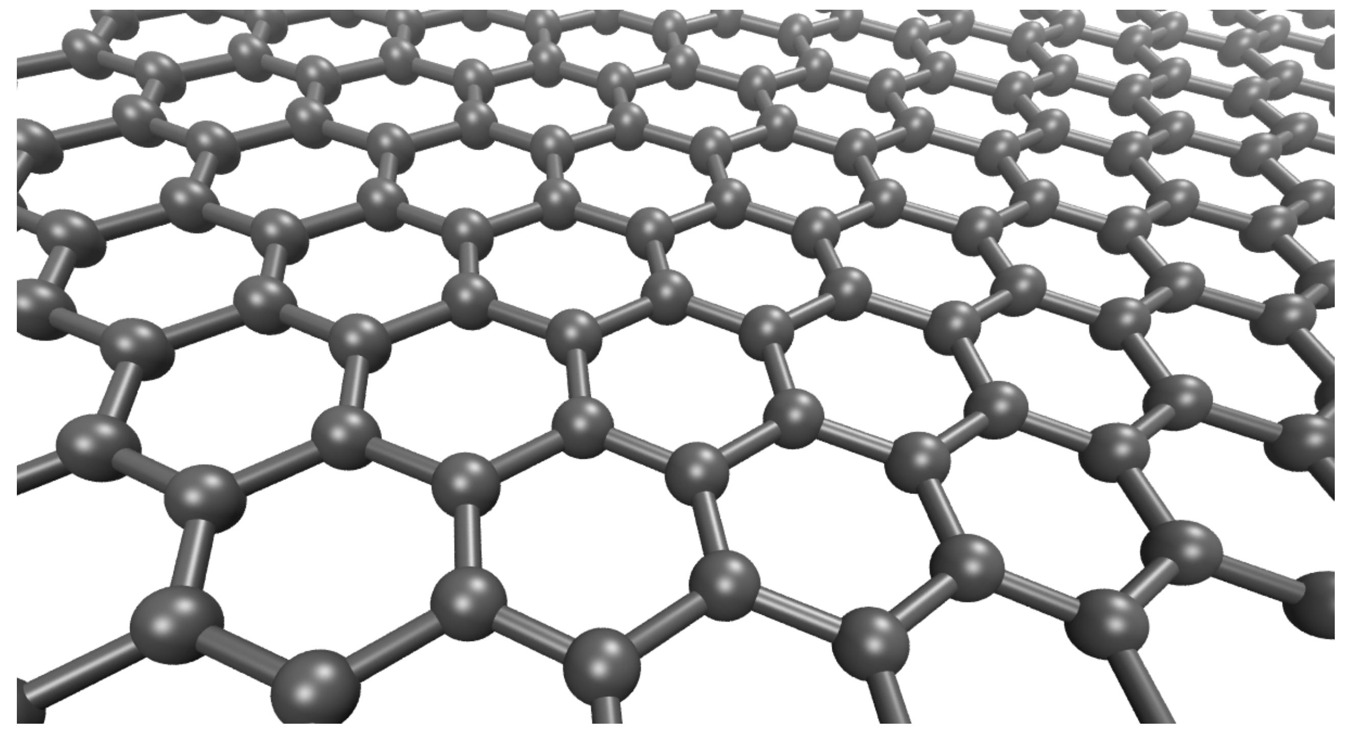
Figure 2.
Electronic configuration diagram vs energy for carbon atom in its (a) ground state and (b) excited state and (c) possible hybridization types: sp (red), sp2 (blue), and sp3 (green).
Figure 2.
Electronic configuration diagram vs energy for carbon atom in its (a) ground state and (b) excited state and (c) possible hybridization types: sp (red), sp2 (blue), and sp3 (green).

Figure 3.
(a) sp hybridization scheme and (b) resulting electronic configuration with hybrid orbitals, (c) geometry of sp orbitals, and (d) example of such hybridization in ethyne molecule.
Figure 3.
(a) sp hybridization scheme and (b) resulting electronic configuration with hybrid orbitals, (c) geometry of sp orbitals, and (d) example of such hybridization in ethyne molecule.

Figure 4.
(a) sp2 hybridization scheme and (b) resulting electronic configuration with hybrid orbitals, (c) geometry of sp2 orbitals, and (d) example of such hybridization in ethene molecule.
Figure 4.
(a) sp2 hybridization scheme and (b) resulting electronic configuration with hybrid orbitals, (c) geometry of sp2 orbitals, and (d) example of such hybridization in ethene molecule.

Figure 5.
(a) sp3 hybridization scheme and (b) resulting electronic configuration with hybrid orbitals, (c) geometry of sp3 orbitals, and (d) example of such hybridization in ethane molecule.
Figure 5.
(a) sp3 hybridization scheme and (b) resulting electronic configuration with hybrid orbitals, (c) geometry of sp3 orbitals, and (d) example of such hybridization in ethane molecule.
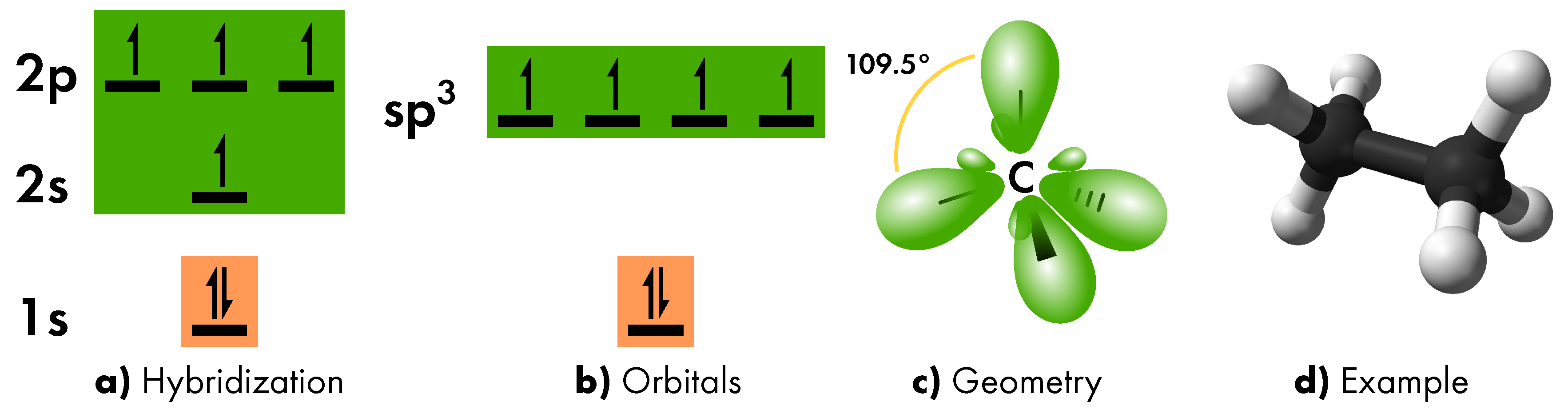
Figure 6.
Exemplary ball and stick model of (a) diamond and (b) graphite.
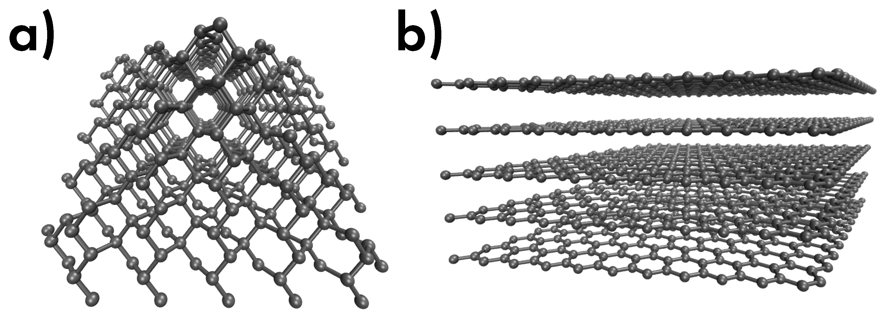
Figure 7.
Ball and stick models of (a) fullerene, (b) carbon nanotubes, and (c) graphene.

Figure 8.
(a) Hexagonal structure of graphene in the real space. The atoms are distinguished in accordance to the two sub-lattices A (green) and B (red) to which they belong. Primitive vectors ( and ) and first near-neighbor vectors (, and ) are marked. The primitive cell (PC) is highlighted. (b) Corresponding reciprocal lattice of graphene. Primitive vectors ( and ), and the high-symmetry points , , , and (yellow) are marked. The PC and the first Brillouin zone (BZ) are highlighted. Adapted with permission from Ref. [23]. Copyright (2009) American Physical Society.

Figure 9.
2D (a), and 3D (b) surface plots of graphene energy bands for finite values of coefficients in Equation (19) equal to 2.7 eV and 0.2t and 0. High-symmetry point , , , and in the first Brillouin zone (white hexagon) are marked by labels
Figure 9.
2D (a), and 3D (b) surface plots of graphene energy bands for finite values of coefficients in Equation (19) equal to 2.7 eV and 0.2t and 0. High-symmetry point , , , and in the first Brillouin zone (white hexagon) are marked by labels

Figure 10.
DOS of graphene calculated by assuming (a) , and (b) in Equation (19). (c,d) Detailed plot of energy near . Reprinted with permission from Ref. [23]. Copyright (2009) American Physical Society.

Figure 11.
(a) Diagram of intraband light absorption transitions at the point of graphene Brillouin zone. In particular, absorption of photons at various energies (ℏω, continuous arrows), and phonon and defect-assisted scattering (k, dashed arrows) are depicted. (b) Diagram of interband light absorption transitions at the and points. In particular, absorption of photons at various energies (ℏω), for allowed and forbidden transitions are depicted. Adapted with permission from Ref. [22]. Copyright (2012) Elsevier. (c) Light absorption of graphene in the far-infrared (FIR), mid-infrared (MIR), near-infrared (NIR), visible (VIS) regions due to intraband and interband transitions at the point. The effect of non-null graphene Fermi Energy determines the enhancement of absorption in the FIR region and the quenching in the MIR due to oscillator-strength sum rule and Pauli blocking, respectively. The absorption band in VIS-UV region due to the transition at point is also reported.

Figure 12.
(a) Diagram and (b) spectra of photoluminescence thermalized electrons in graphene. Reprinted with permission from Ref. [50]. Copyright (2017) American Chemical Society. (c) Diagram and (d) spectra of photoluminescence non-thermalized electrons in graphene. Reprinted with permission from Ref. [22]. Copyright (2012) Elsevier.

Figure 13.
(a) Raman spectra of (from top to bottom) monolayer graphene, highly oriented pyrolytic graphite (HOPG), single-wall carbon nanotube (SWNT), single-wall carbon nanohorns (SWNH) and hydrogenated amorpous carbon. The label for the main bands is reported. Adapted with permission from Ref. [55]. Copyright (2010) American Chemical Society. (b) Raman spectra of defected monolayer graphene. Adapted with permission from Ref. [54]. Copyright (2017) Cambridge University Press.

Figure 14.
(a) Phonon dispersion relation for graphene along the direction connecting the high-symmetry points , , and . The phonon branches are labeled in accordance with their type of atomic displacement. Various Raman contribution is indicated, as well as the corresponding range of phonon wavevector. (b) Phonon density of states (DOS) of graphene. The contribution of Raman mode at different phonon frequency is indicated by color. Adapted with permission from Refs. [56,57]. Copyright (2011) American Physical Society and (2018) Elsevier.
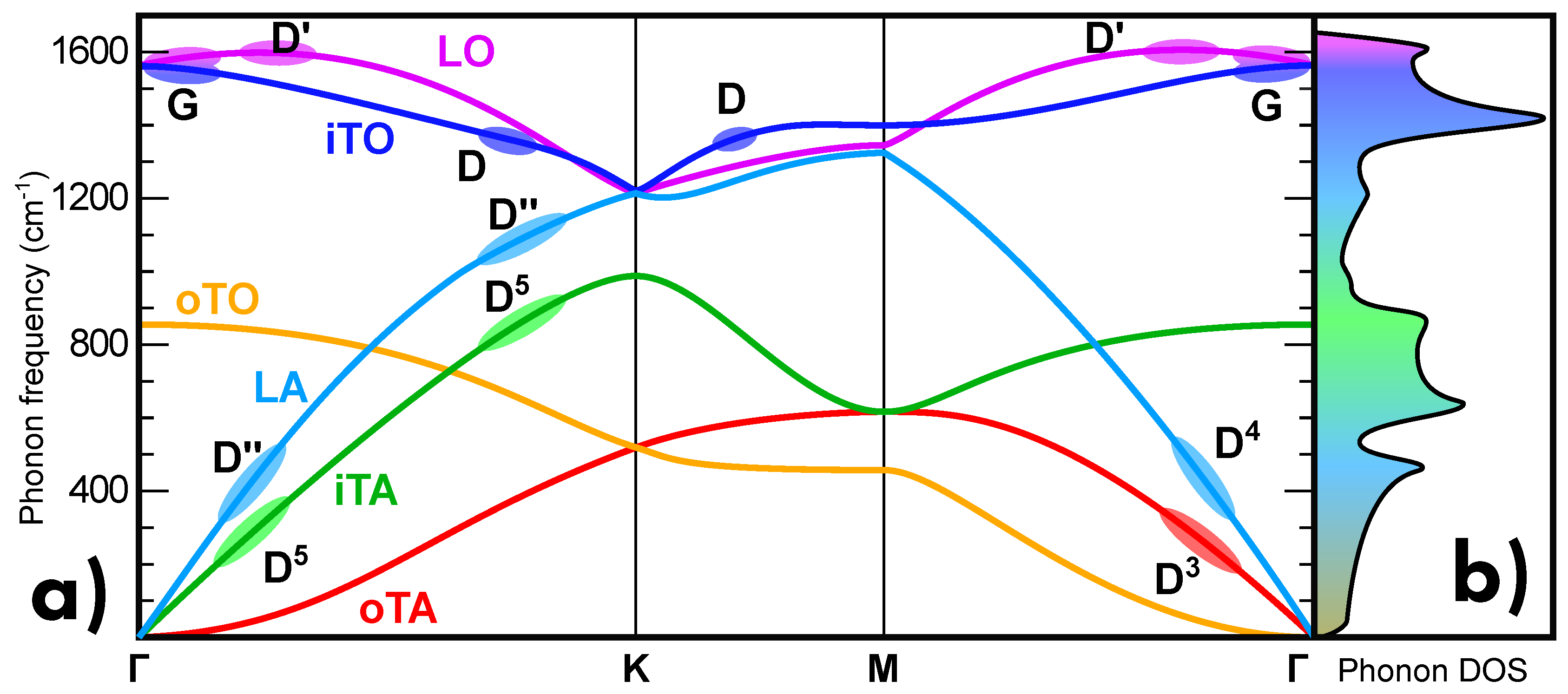
Figure 15.
Phonon modes of single-layer graphene at wavevector equal to (a) and (b) . Each mode is indicated by the symmetry of wavevector, the space group label in Mulliken notation, and by the type of the corresponding atom displacement. Adapted with permission from Ref. [54]. Copyright (2017) Cambridge University Press.
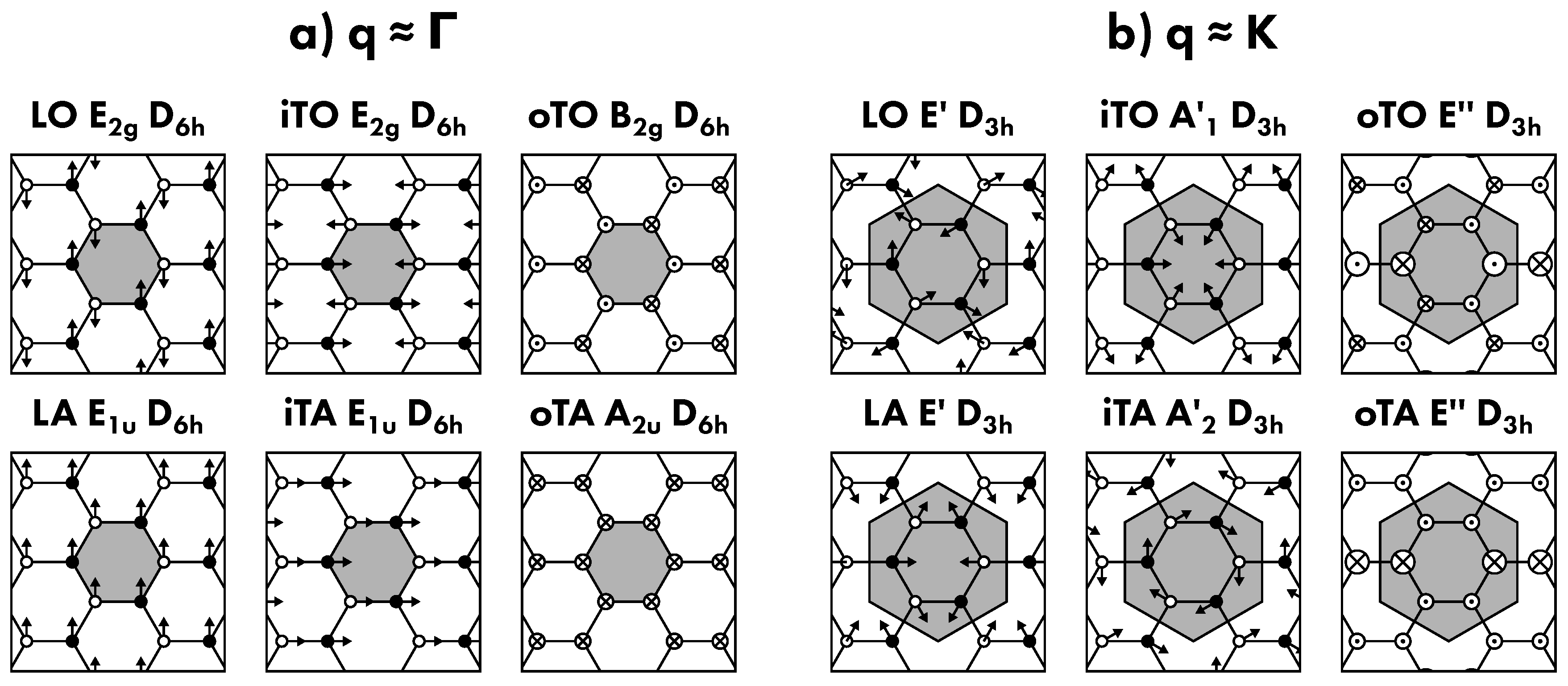
Figure 16.
Raman scattering processes in graphene which determine the (a) G band, (b,c) D’ band, (d) 2D’ band, (e) D band, (f,g) 2D and D + D” bands, and (h) D + D’ band. The light induced electron-hole pair generation and the following recombination are indicated by blue and red arrows, respectively, whereas the phonon () and the defect () scattering are indicated by dashed and dotted arrows, respectively. Adapted with permission from Ref. [58]. Copyright (2013) Springer Nature.

Figure 17.
(a) Scheme of laser energy influence on scattering process for 2D mode (b) Peak position dispersion of D + D” and 2D bands for various laser energies. Reprinted with permission from Ref. [59]. Copyright (2007) American Physical Society. (c) Intensity change of G band for increasing laser energy, whereas the other resonant bands do not show any enhancement. Adapted with permission from Ref. [53]. Copyright (2017) Wiley. (d) Heat dissipation for suspended and supported graphene. (e) Shift of G peak position as effect of laser power. Reprinted with permission from Ref. [61]. Copyright (2008) American Chemical Society.

Figure 18.
Evolution of (a) optical contrast and (b,c) G band intensity of graphene by increasing the number of layers. Panels (a,b) are reprinted with permission from Ref. [68]. Copyright (2018) Wiley. Panel (c) is reprinted from Ref. [67]. Copyright (2007) American Chemical Society.

Figure 19.
(a) Lorentzian component of 2D band for single-layer graphene, multi-layer graphene and HOPG characterized by various numbers of layer. Reprinted with permission from Ref. [70]. Copyright (2010) American Institute of Physics. (b) Splitting of conduction and valence band of two-layer graphene where four 2D scattering processes are possible. Adapted with permission from Ref. [42]. Copyright (2013) Wiley.

Figure 20.
(a) Scheme of Fermi velocity influence on scattering process for 2D mode related to graphene folding. (b) Raman spectra of folded graphene compared to single- and double-layer graphene. Adapted with permission from Ref. [71]. Copyright (2008) American Physical Society.
Figure 20.
(a) Scheme of Fermi velocity influence on scattering process for 2D mode related to graphene folding. (b) Raman spectra of folded graphene compared to single- and double-layer graphene. Adapted with permission from Ref. [71]. Copyright (2008) American Physical Society.

Figure 21.
Typical defects in graphene: (a) pristine graphene, (b) monovacancy defect, (c) double-vacancy defect, (d) 555-777 defect, (e) 5555-6-7777 defect, and (f) Stone-Wales defect. Adapted with permission from Ref. [72]. Copyright (2013) American Chemical Society. (g) Representative model of graphene oxide. Adapted with permission from Ref. [89]. Copyright (1998) Elsevier. (h) Raman spectrum of graphene subjected to ion bombardment at various irradiation doses (1011, 1012, ... Ar ions cm−2). (i) Relative intensity between D and G bands (ID/IG) on increasing the interdefect distance LD. Adapted with permission from Ref. [87]. Copyright (2010) Elsevier.

Figure 22.
(a) Different edge structures for graphene: zigzag (blue) and armchair (red), and their respective momenta transferred to scattered electrons ( and ). (b) Wavevector change by scattering at different types of edge, and consequent contribution to Raman scattering bands. Adapted with permission from Ref. [53]. Copyright (2011) Wiley.

Figure 23.
(a) Raman spectra of defective graphene produced by fluorination (saturated defects) and anodic bonding (unsaturated defects). (b) Linear dependence between the ID/ID’ ratio for graphene featuring different types of defects. Adapted with permission from Ref. [92]. Copyright (2012) American Chemical Society.
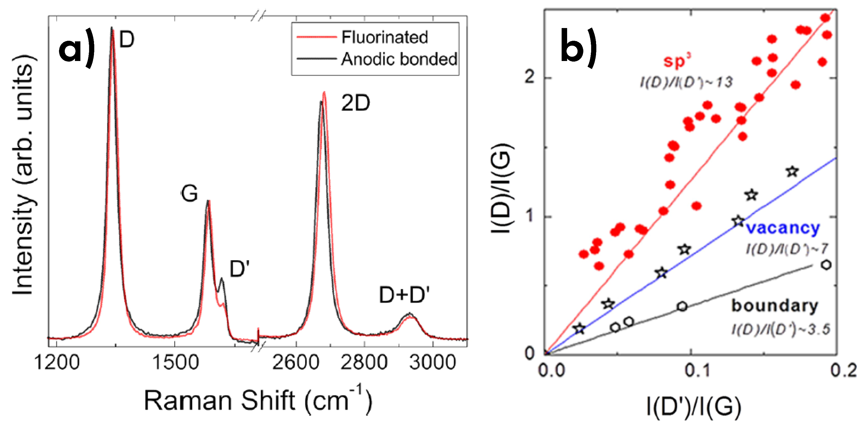
Figure 24.
Modification of peak frequency of (a) G, and (b) 2D bands as effect of uniaxial strain. In the former panel, the splitting of G band in the two G+ and G– bands can be observed. Reprinted with permission from Ref. [98]. Copyright (2009) American Physical Society.
Figure 24.
Modification of peak frequency of (a) G, and (b) 2D bands as effect of uniaxial strain. In the former panel, the splitting of G band in the two G+ and G– bands can be observed. Reprinted with permission from Ref. [98]. Copyright (2009) American Physical Society.

Figure 25.
(a) Interaction between phonon and virtual electron-hole pair. Modification of (b) bandwidth (c) peak frequency for G band on varying doping. Adapted with permission from Ref. [101]. Copyright (2006) American Physical Society.
Figure 25.
(a) Interaction between phonon and virtual electron-hole pair. Modification of (b) bandwidth (c) peak frequency for G band on varying doping. Adapted with permission from Ref. [101]. Copyright (2006) American Physical Society.
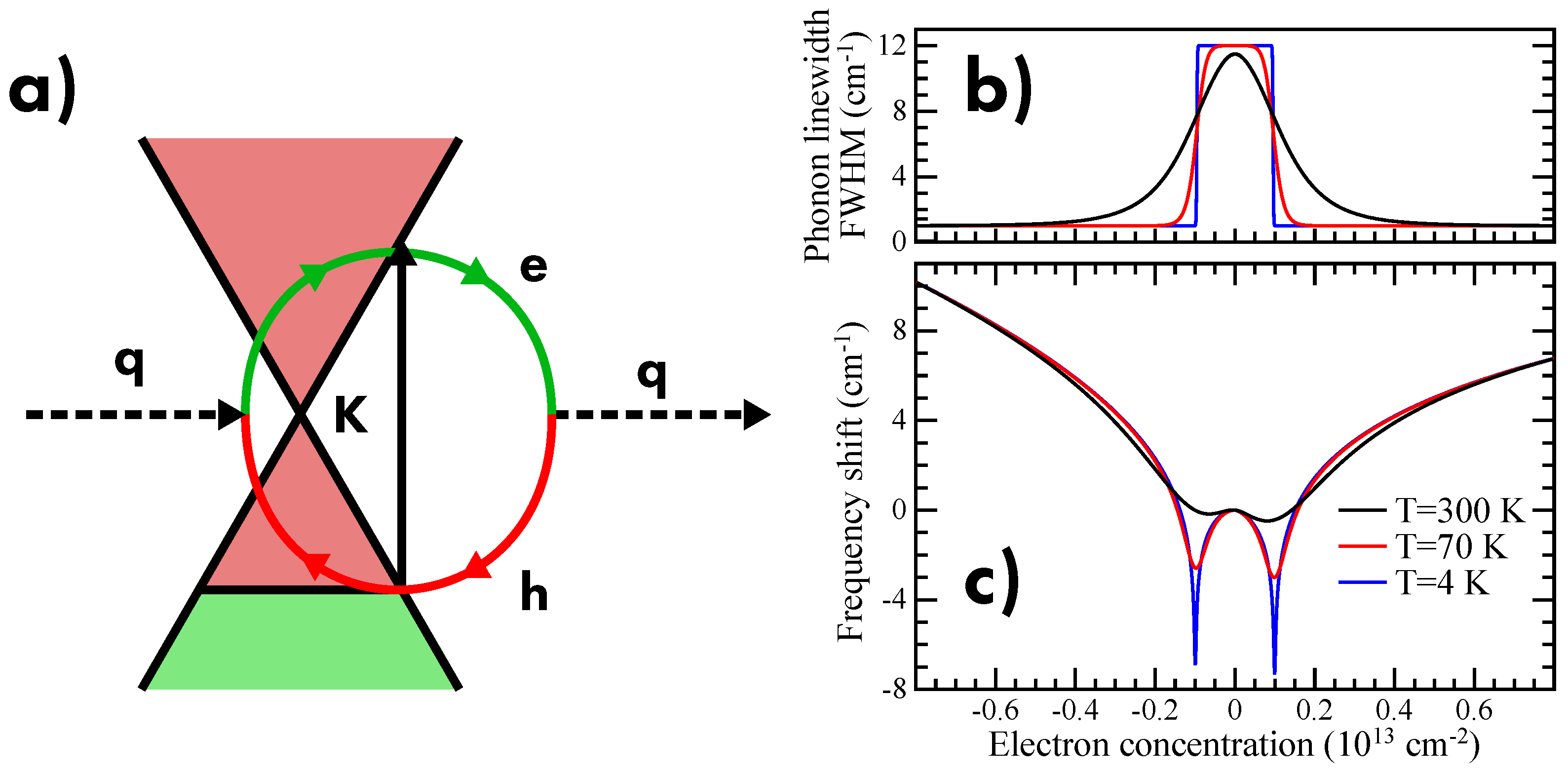
Figure 26.
Modification of peak frequency of (a) G band and (b) 2D band, (c) G bandwidth, and (d) ratio between G and 2D integrated intensity for graphene doped by gate voltage application. Reprinted with permission from Ref. [102]. Copyright (2008) Springer Nature.
Figure 26.
Modification of peak frequency of (a) G band and (b) 2D band, (c) G bandwidth, and (d) ratio between G and 2D integrated intensity for graphene doped by gate voltage application. Reprinted with permission from Ref. [102]. Copyright (2008) Springer Nature.
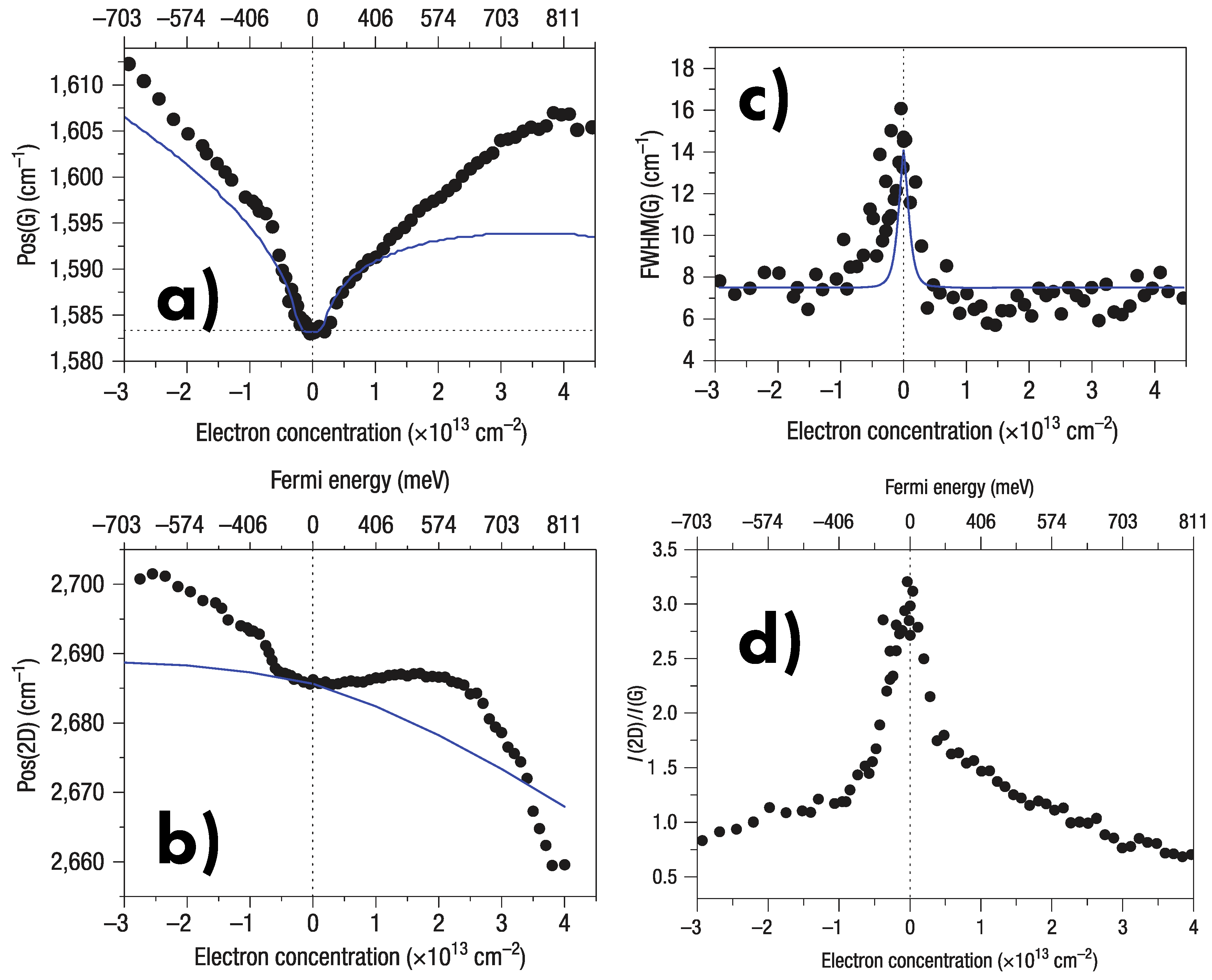
Figure 27.
(a) G-2D map of graphene in various doping and strain configurations. Each point corresponds to a given G and 2D peak position extracted from a given spectrum. The map is described by three independent axes: doping (n) by distinguishing between p (red) or n (blue) doping, strain (ε), and Fermi velocity variation (ΔvF/vF, black) (b) doping influence on I2D/IG. Adapted with permission from Ref. [109]. Copyright (2013) American Chemical Society.

Figure 28.
Representative depiction of graphene produced by (a) mechanical exfoliation, (b) liquid-phase exfoliation, (c) electrochemical exfoliation, and (d) reduced graphene oxide (rGO) obtained from graphene oxide (GO).
Figure 28.
Representative depiction of graphene produced by (a) mechanical exfoliation, (b) liquid-phase exfoliation, (c) electrochemical exfoliation, and (d) reduced graphene oxide (rGO) obtained from graphene oxide (GO).
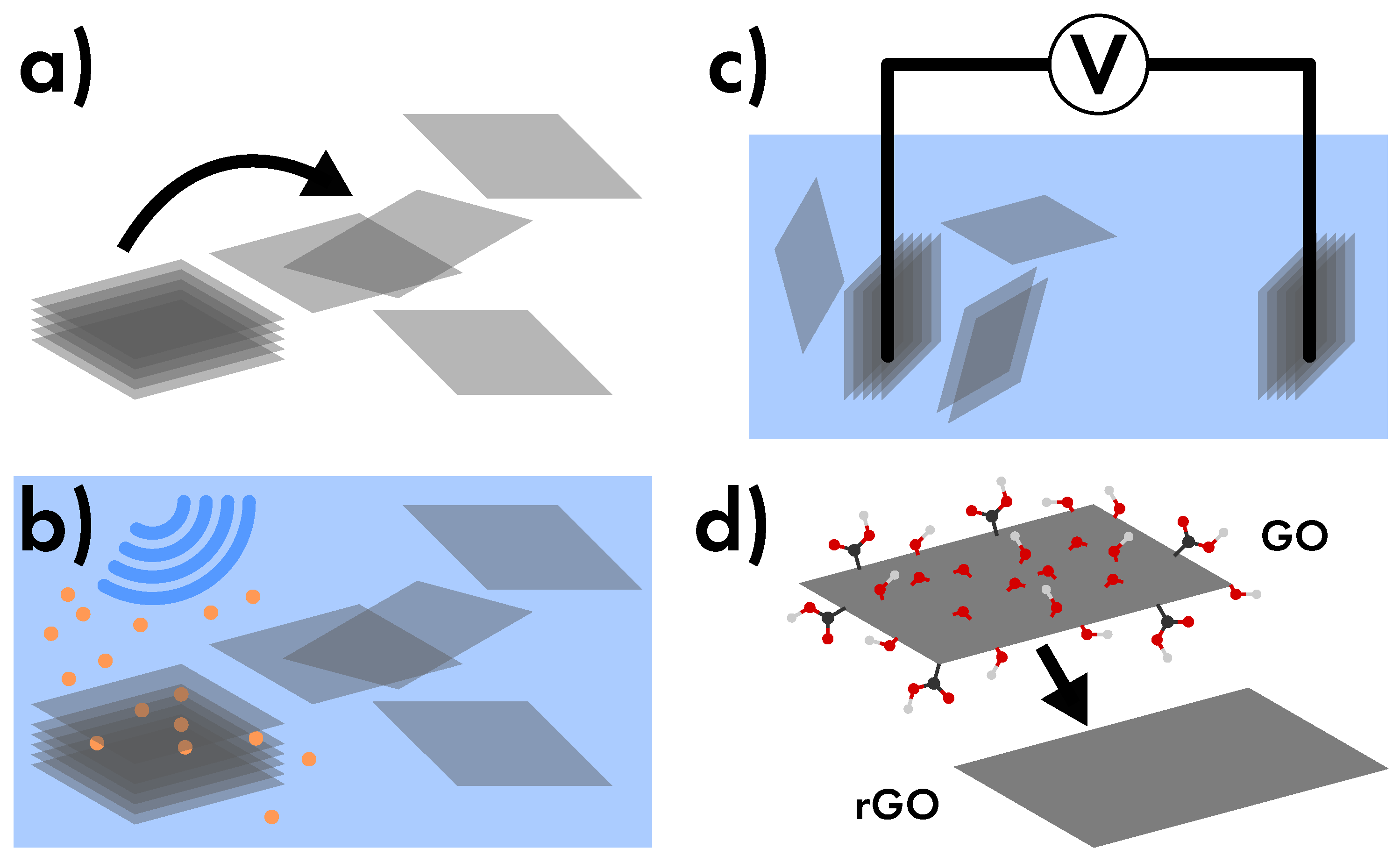
Figure 29.
Representative depiction of graphene (Gr) or N-doped graphene (N-doped Gr) produced by (a) chemical vapor deposition, (b) thermal annealing of amorphous carbon (am-C) (c) solvothermal synthesis, and (d) epitaxial growth on .
Figure 29.
Representative depiction of graphene (Gr) or N-doped graphene (N-doped Gr) produced by (a) chemical vapor deposition, (b) thermal annealing of amorphous carbon (am-C) (c) solvothermal synthesis, and (d) epitaxial growth on .

© 2019 by the authors. Licensee MDPI, Basel, Switzerland. This article is an open access article distributed under the terms and conditions of the Creative Commons Attribution (CC BY) license (http://creativecommons.org/licenses/by/4.0/).
Share and Cite
MDPI and ACS Style
Armano, A.; Agnello, S. Two-Dimensional Carbon: A Review of Synthesis Methods, and Electronic, Optical, and Vibrational Properties of Single-Layer Graphene. C 2019, 5, 67. https://0-doi-org.brum.beds.ac.uk/10.3390/c5040067
AMA Style
Armano A, Agnello S. Two-Dimensional Carbon: A Review of Synthesis Methods, and Electronic, Optical, and Vibrational Properties of Single-Layer Graphene. C. 2019; 5(4):67. https://0-doi-org.brum.beds.ac.uk/10.3390/c5040067
Chicago/Turabian StyleArmano, Angelo, and Simonpietro Agnello. 2019. "Two-Dimensional Carbon: A Review of Synthesis Methods, and Electronic, Optical, and Vibrational Properties of Single-Layer Graphene" C 5, no. 4: 67. https://0-doi-org.brum.beds.ac.uk/10.3390/c5040067
Note that from the first issue of 2016, this journal uses article numbers instead of page numbers. See further details here.