Effects of the Stacking Faults on the Electrical Resistance of Highly Ordered Graphite Bulk Samples


Division of Superconductivity and Magnetism, Felix Bloch Institute for Solid State Physics, Linnéstrasse 5, University of Leipzig, 04103 Leipzig, Germany
*
Author to whom correspondence should be addressed.
C 2020, 6(3), 49; https://0-doi-org.brum.beds.ac.uk/10.3390/c6030049
Submission received: 1 July 2020
/
Revised: 21 July 2020
/
Accepted: 23 July 2020
/
Published: 25 July 2020
(This article belongs to the Collection Nanocarbon-Based Composites and Their Thermal, Electrical, and Mechanical Properties)
Abstract
:High anisotropy and the existence of two-dimensional highly conducting interfaces at stacking faults parallel to the graphene planes of the graphite structure influence, in a non-simple way, the transport properties of highly oriented graphite. We report two related effects on the electrical resistance of highly oriented pyrolytic as well as of natural graphite bulk samples, measured with the four points method in the temperature range 300 K 410 K. A qualitative and quantitative change in the temperature dependence of the resistance was obtained by simply enlarging the electrodes and contacting the edges of the internal interfaces on the same sample. Additionally, at temperatures K the resistance can change with time. We show that this temperature-dependent annealing effect is related to the stacking faults and can irreversibly change the absolute value of the resistance and its temperature dependence. A partial recovery is obtained after leaving the sample at normal conditions for several days. The overall results stress the importance of the electrodes location on a bulk graphite sample, the contribution of the stacking faults in the interpretation of the measured transport properties and the need of systematic studies on the influence of high temperature annealing on the interfaces properties.
1. Introduction
The electrical conductivity of carbon-based compounds, especially graphite, has been reported in a large number of studies in the last nearly 90 years, see in [1,2] and the references therein. Detailed studies of carbonaceous powders under different compaction pointed out the existence of different contributions to, and the complexity of, the electrical conductivity [3] as well as the effect of oxygen on it [4]. In highly oriented graphite samples with the narrowest rocking curve width, the typical size of the single crystalline regions, in the direction parallel to the graphene planes, is of the order of micrometers [5]. Therefore, the electrical resistance of bulk samples of much larger size would have the intrinsic contribution of the graphene layers added to that of the grain boundaries. There is, however, a further effect that makes the estimate of the intrinsic resistivity difficult, namely, the large anisotropy of the electrical resistivity of graphite with its c-axis resistivity being much larger than the in-plane one . This anisotropy was already reported at the end of the 1930s [6]. Although its value is sample-dependent due to the influence of defective regions in the samples, there is consent among different publications that the ratio . This anisotropy implies that the input current has a relatively small penetration depth in the axis direction, when the electrodes are located, e.g., at the top surface of a well-ordered graphite sample. Would a graphite sample be homogeneous from the structural and electrical point of view, i.e., with only one of the two possible stacking orders and without twisted regions around the common axis, then we expect to have similar results for the normalized resistance obtained by placing the electrodes at the sample top surface or at the sample edges. As we report in this study, this does not occur in graphite samples of large enough thickness due to the contribution of highly conducting stacking faults to the total sample conductance.
The existence of stacking faults or two-dimensional (2D) interfaces in well-ordered graphite samples has been recently reported by transmission electron microscopy (TEM) [7,8]. These TEM images together with high-resolution X-ray diffraction (XRD) [9] as well as transport measurements [7,8] revealed that most, if not all, thick enough highly ordered graphite samples have 2D stacking faults located between twisted crystalline regions with the same or different stacking orders. These faults can be embedded within the multilayer graphene matrix and can be found even at the sample surface [7,8,9,10,11,12]. These “interfaces” show qualitative different transport properties than those of the graphene planes in any of the two graphite stacking orders, i.e., Bernal and rhombohedral. Taking into account the electronic band structure at the interfaces between twisted graphite regions [10,13,14,15] or between the two stacking orders of graphite [16,17,18], such a difference in the transport properties is not surprising. For example, a recently published experiment was able to contact the edge of a relatively thin graphite sample, and thereby its embedded interfaces [19]. The obtained value of for the (metalliclike) rest-resistance-ratio as well as the positive magnetoresistance of ≃10 at 21 T, at temperatures below 1K, are record-breaking values that emphasized the need to take into account these interfaces in the interpretation of the transport properties.
Previous transport studies revealed the influence of the 2D stacking faults on the transport properties below 300 K of mesoscopic, thin (thickness nm and several m area) graphite samples by nanometer thickness reduction [20]. In this work, we are interested on the influence of the 2D interfaces on bulk samples, in particular in the temperature range above 300 K because of the expected superconducting [9,17,21,22,23,24] and/or magnetic transitions [25]. With a simple experimental approach and without the need of etching, lithography, or both processes, we show that the contribution of the interfaces can change qualitatively and quantitatively the resistance of a bulk graphite sample. Furthermore, at temperatures above ~ K we found that the resistance shows a non-monotonic change with time. We show that this high temperature effects are directly related to changes at the interfaces.
2. Materials and Methods
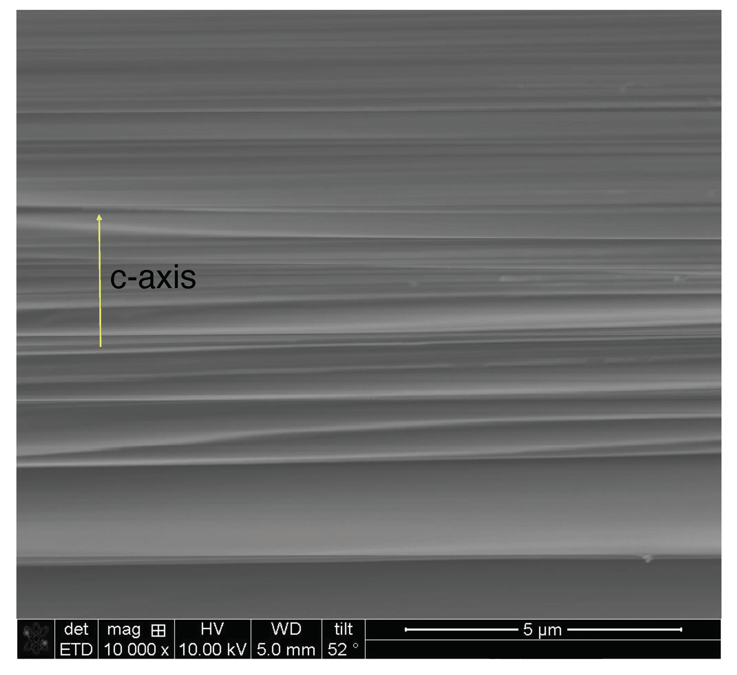
The main characteristics and dimensions of the measured samples in this work are listed in Table 1. Figure 1 shows a scanning electron microscope image taken directly at the edge of a bulk HOPG sample. One can recognize openings between regions of different gray color. Each of these regions can have a thickness from several tens to hundreds of nm, mostly with the Bernal stacking order, as TEM images revealed [7,26,27]. Regions with the minority rhombohedral stacking order phase also exist but are in general thinner [9,28].
The electrical resistance was measured using an AC LR700 resistance bridge (four points method) with a frequency of 16 Hz and input currents A. To measure the electrical resistance as a function of temperature we have used two devices. The graphite sample in the device called minicryo was in a vacuum of mbar during the measurements and attached to a small and high efficient cryocooler, with small thermal mass and consumption; for more details see in [30]. The sample thermometer was fixed on the same Cu-block where the sample was attached. The heater for the temperature stabilization was fixed around the main cooling finger, where at its top the sample/thermometer holder was.
The second device used was the main sample temperature stabilization space of a He-flow cryostat from Quantum Design with a sample holder that allowed also four points measurements of the electrical resistance. The temperature was measured and set with the available thermometer and stabilization program. In this device, the sample is not in vacuum but in a ~ mbar He atmosphere.
3. Results
3.1. Resistance before and after Contacting the Edge of a Graphite Sample
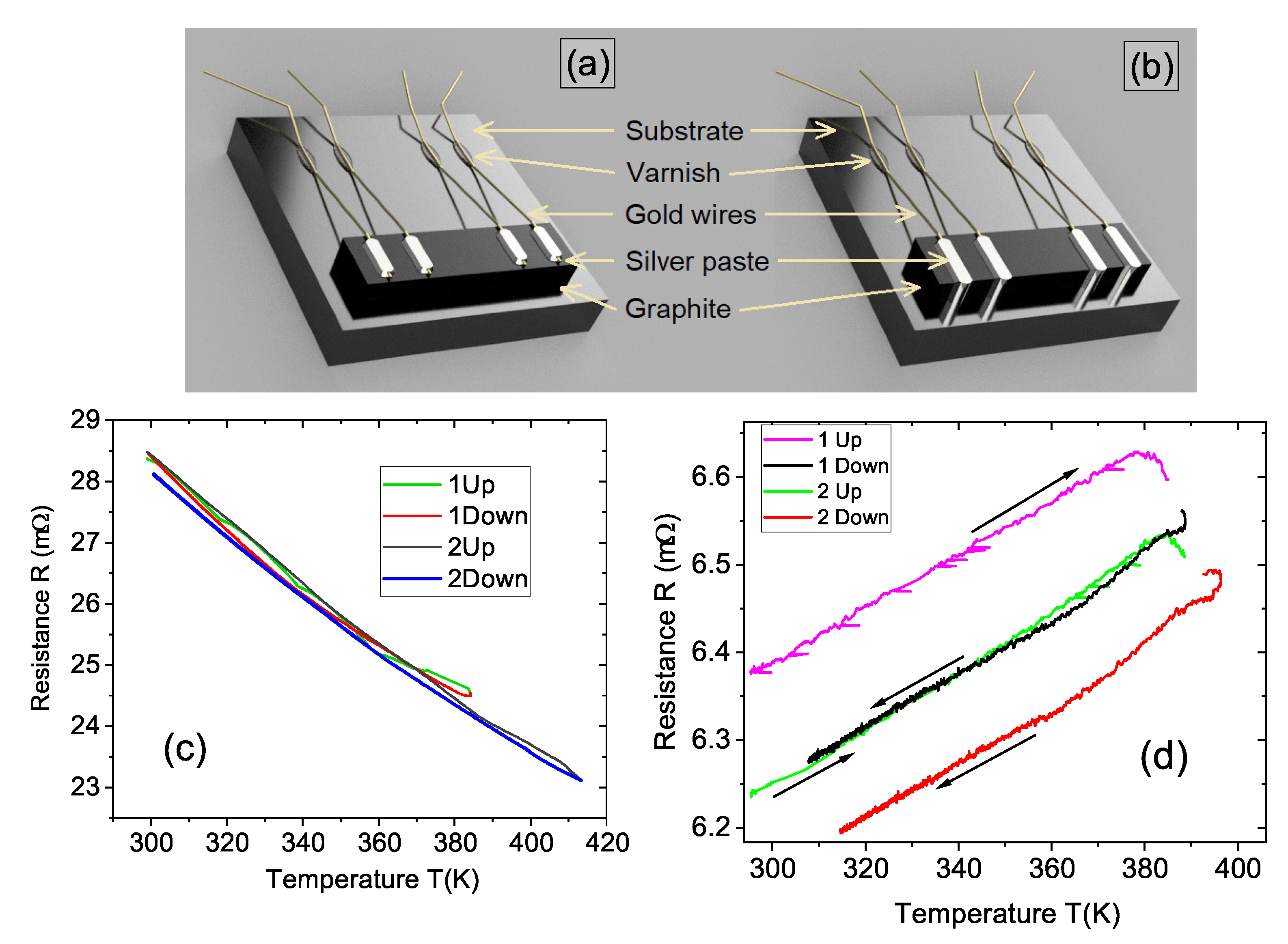
Several transport studies of different highly ordered graphite samples, from thin flakes of thickness nm to bulk samples, indicate that the intrinsic electronic transport in ideal graphite is semiconducting-like. This means that the resistance decreases with temperature following a typical exponential function having energy gaps between eV for the Bernal stacking order and ≃eV for the rhombohedral one [8,31]. The metallic-like part, which is measured in thick enough samples, is related to the contribution of 2D interfaces between regions of different stacking orders or twisted regions around a common axis [20]. This means that in a sample where the interfaces are located far away from the sample surface, i.e., at distances larger than the current penetration depth in the axis direction, we would expect that the resistance measured with the contacts at the top surface, as shown in the sketch of Figure 2a, shows a semiconducting-like behavior. Indeed, this is the case as we can see in Figure 2c. Note also that the irreversibility in the temperature loops is small and no time dependence is observed within experimental error, especially at high temperatures.
After we finished with the measurements shown in Figure 2c, we took out the sample from the cryostat and the electrical contacts were enlarged, contacting especially the side edge of the sample as sketched in Figure 2b. After waiting two days to dry the electrodes, the resistance was measured again during heating and cooling temperature cycles as shown in Figure 2d. Several remarkable changes were observed. First, the absolute value of the resistance at the beginning of the measurements was smaller by a factor 4. This decrease in the absolute resistance is not surprising because we are getting the contribution of several graphene layers in parallel contacting all their edges. However, the qualitative difference in the temperature dependence, a metallic-like dependence, can be interpreted as due to the contribution of certain stacking faults running in parallel to the graphene layers. It is also remarkable that the resistance decreases with time at temperatures above ≃380 K, whereas, for this sample, the temperature dependence below 380 K does not change significantly. Evidently, this decrease at high enough temperatures is related to the contribution of certain interfaces and it is observed in all bulk samples, as we show below in the next sections. It is important to mention that the observed changes are not related to the contacts; these were already several days old and any drying process should not have any influence on the measured resistance. As we will see below, the changes produced by annealing are reversible after leaving the sample at normal conditions for several days, ruling out contact problems as well.
The observed changes in the absolute values of the resistance already emphasize the inaccuracy one has when one needs an estimate of the intrinsic resistivity of graphite. For example, assuming an electrically homogeneous sample without electrical anisotropy, from the results of Figure 2 at 300 K we estimate a resistivity Kcm (electrodes at the top, case (c)) and ∼cm (electrodes at the top and side, case (d)). Those values are within those reported in the literature for highly ordered graphite bulk samples [1,2]. Much smaller values are obtained in case (c) if we assume a much smaller thickness due to the finite penetration depth (∼ nm at low temperatures [20]). The intrinsic resistivity value for ideal graphite was estimated in [20] to be Kcm. The resistivity values in our sample are evidently smaller but not very different. The reasons for this relatively small difference are (1) the contribution of the 2D interfaces to the total conductance depends on temperature, getting weaker the higher the temperature [19,31], and (2) the electrical anisotropy also decreases with temperature.
Concluding this section, it should be clear that the temperature dependence of the resistance of bulk graphite samples is not unique but it depends on the location of the electrodes within the sample in a non-simple way, due to the high electrical anisotropy and the metallic-like contribution of certain interfaces embedded within the graphite structure. Upon the interface distribution within a sample, different and non-simple temperature behavior can be expected, in agreement with the results reported in [20], decreasing systematically the thickness of mesoscopic graphite samples.
3.2. High-Temperature Annealing Effects on the Resistance
Annealing effects in the diamagnetic susceptibility of bulk graphite at K have been already reported that showed an irreversibly decrease in the total diamagnetic signal [32]. We note that a significant part of the diamagnetic response of bulk graphite samples is not due to the graphene planes but to embedded interfaces at some stacking faults, as recently done studies reported [33]. In this section, we demonstrate and discuss the partially subtle effects of time and temperature on the resistance observed at K. For these measurements, we took a new natural graphite bulk sample (#2) with electrodes contacting its edges and fixed in the sample holder of the He-flow cryostat. Although in this cryostat there is no thermometer attached directly on the sample holder, it allows larger temperature changes in less amount of time. To check whether the sample reached the selected temperature, the measurement of its time dependence is necessary.
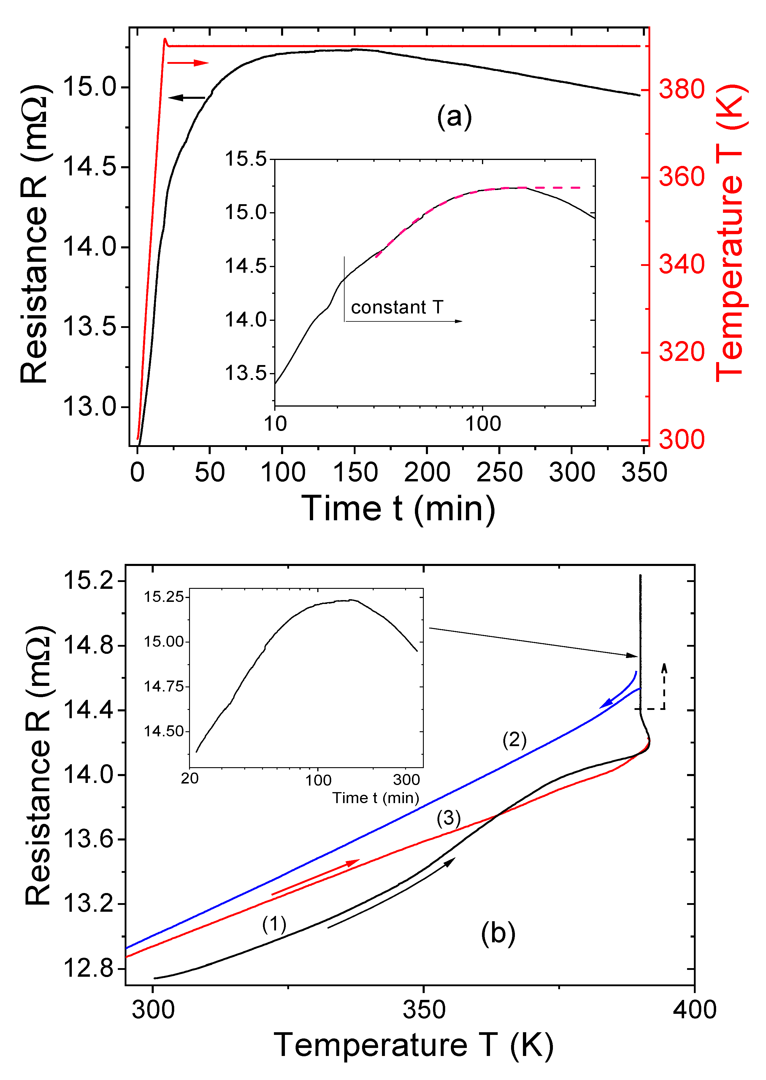
We programmed an increase in the thermometer temperature from 300 K to 390 K within 20 min, as shown by the red line in Figure 3a (right axis). After this temperature was reached at the thermometer, with a small overshoot recognized in Figure 3a, it remained constant within K. As expected for this sample, the measured resistance (black curve in Figure 3a (left axis)) increases, from which we infer that the sample temperature also increases but with a certain delay. Note that the temperature overshoot at approximately min is also observed in the resistance with a short delay, see inset in Figure 3a. After reaching a constant thermometer temperature (region of constant T labeled in the inset) the time-dependent slope of the resistance changes, and at min we observe a second change in the slope. From the data and the experience obtained from magnetization measurements with the same temperature inset, we estimate the delay between the thermometer and sample temperature to be of the order of min for this especial quick heating ramp. This means that at min, the sample temperature can be considered as constant. Nevertheless, the resistance increases following an exponential function min with a relaxation time of min, as shown by the dashed red line in the inset. At min, the resistance starts to decrease with a larger, temperature-dependent relaxation time, as we show in more detail in Figure 4 below. Note that in usual experiments even at these temperatures, one measures the resistance at smaller temperature steps taking a point after a waiting time of the order of 15 min. This means that this subtle increase in resistance is not always easily recognized. Annealing effects on the electrical resistance above room temperature are nowadays of importance because they can detrimentally influence the transition in the resistance observed at K reported in [9,24].
Figure 3b shows the measured resistance vs. temperature from 300 K to 390 K with a warming rate of 5 K/min for sample #2. In the virgin, non-annealed state the sample resistance increases with T, while showing a change in its slope at ∼K and at ∼K. This behavior has been already reported and interpreted as a possible superconducting-like transition with a critical temperature of ∼K [9,24]. We note that in those publications, a similar curve was obtained stabilizing the temperature for 15 min before taking a point. After the small temperature overshoot clearly observed in the resistance, see Figure 3b, we measured the resistance vs. time at 390 K. The sample temperature reached a constant value in the region described by the dashed line in Figure 3b. In the inset we show the time dependence of the resistance in a semilogarithmic scale in the time region where the sample temperature remained constant at K, similar to that shown in the inset of Figure 3a.
After h at K, we started to cool down the sample and measured its temperature dependence before the resistance decreases below a certain value, in order to check whether the increase in the resistance with time remains at lower temperatures. The blue curve (2) in Figure 3b shows that the resistance was larger than the one measured at the first warming, shown by curve (1). Note that the resistance in curve (2) does not show any change in its slope at K, in contrast to curve (1). After cooling it down to 30 K the resistance was again measured to 390 K with similar rate. The result is shown by curve (3) in Figure 3b. We note that this curve does not show any change in its slope around 350 K, indicating that the anomaly at this temperature measured in the virgin state vanished after the temperature cycle.
The results of this temperature cycle clearly indicate that the temperature annealing to 390 K for several hours was enough to wash out the transition at certain interfaces observed at ∼K in the virgin state. This effect of the temperature hysteresis cycle is in qualitative agreement with the partial vanishing of the diamagnetic signal after increasing the temperature above ∼K in a bulk HOPG sample [32]. All these results stress that the phase that is responsible for the step-like change in the resistance in the virgin curve is very sensitive to high-temperature annealing and care should be taken. This vanishing may provide an answer to the difficulties one has to observe and reproduce the transition in some specific samples.
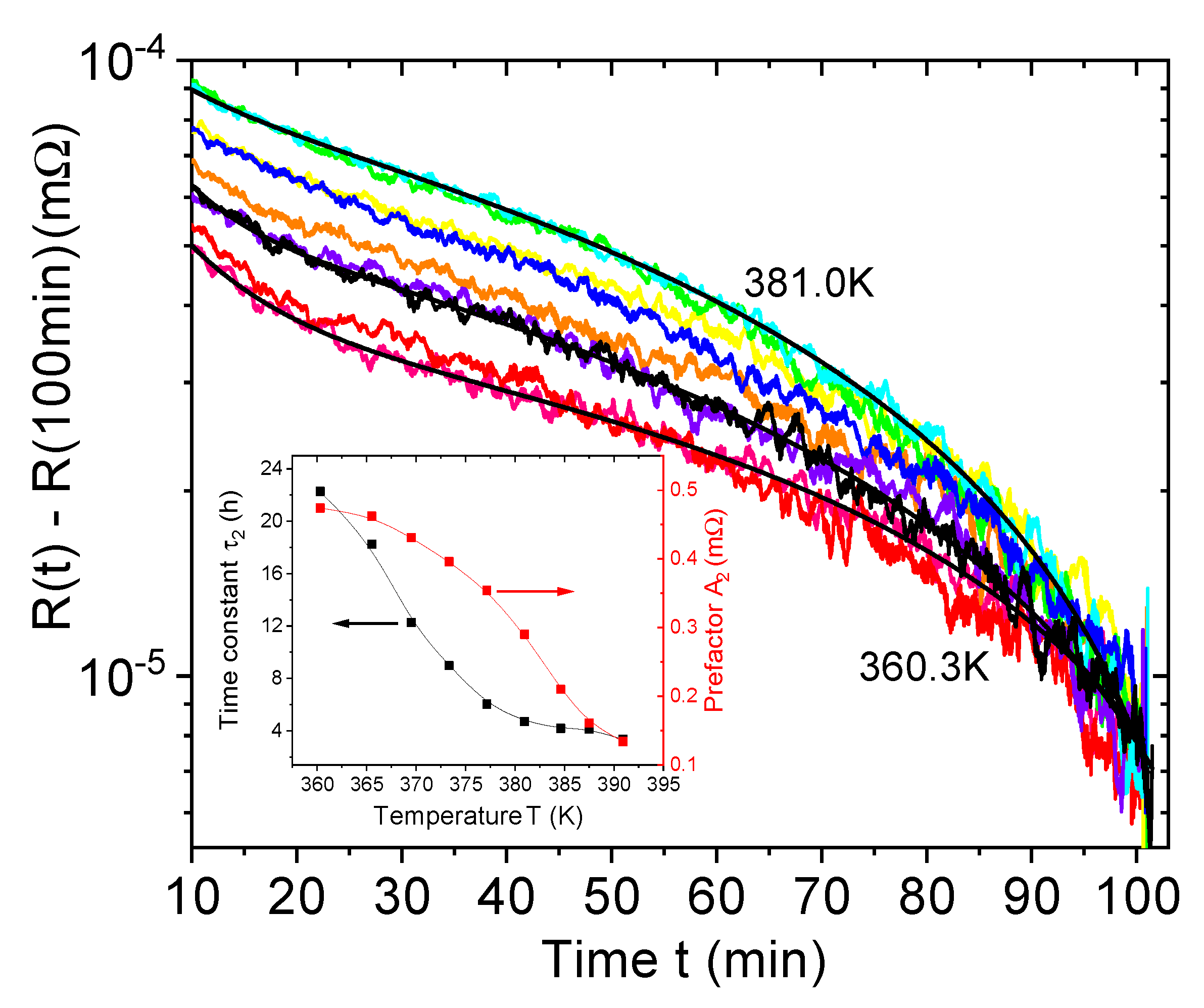
We discuss now the characterization of the relaxation time of the decrease of the resistance at different temperatures at K. For this characterization, we took sample #3 and measured the decrease of its resistance at different constant temperatures in a sequential manner. This means that after ≃min, and after a certain decrease in the resistance was measured, we increased the temperature and started again with the time measurement. Note that the sample did not start at the different selected temperatures in its virgin state. The reason for the selection of this sequential procedure is the large relaxation time necessary for a full recovery of the sample, as we discuss in the next section.
Figure 4 shows the time dependence of the resistance at different constant temperatures. The three continuous curves through the experimental data are fits to the equation , where the prefactors, as well as the relaxation times, are parameters we obtain from the fits. The first relaxation term (subindex 1) represents a rather short relaxation term with a nearly temperature-independent relaxation time, min, with also a nearly constant prefactor, m. This first relaxation is mostly related to a transient related to the temperature stabilization after a temperature step. The second relaxation process shows temperature-dependent relaxation times. The relaxation time as well as the prefactor of this process decrease with temperature, see the inset of Figure 4.
3.3. Influence of Air Atmosphere: Recovery of the Resistance
The observed time relaxation of the resistance at high enough temperatures when one contacts the edges of the samples, indicate that certain diffusion processes at the interfaces play a role. In this section, we demonstrate that there is a recovery of the resistance when one leaves the sample in air at normal atmosphere after the high-temperature annealing. The results indicate that at least part of the relatively large decrease of the resistance at high temperatures can be recovered. Figure 5 shows four temperature cycles (each cycle means K K K) measured after the sample preparation, i.e., starting with the sample in the virgin state. The results are similar to those shown in Figure 2d. We note, however, that the resistance of the sample decreased by a factor of two after the temperature cycles, in contrast to the few percent decrease observed when the maximum temperature of each cycle remains below 390 K; compare the results in Figure 2d with those in Figure 5.
After we reached 290 K, at the end of the fourth temperature cycle starting with the sample in the virgin state, we took the sample out of the minicryo and left it at that temperature in air for two days. Afterwards, we measured its resistance and its temperature dependence within one temperature cycle. The result is the blue curve in Figure 5. We note that the initial resistance at 290 K was clearly higher than just after finishing the previous four cycles. The single temperature cycle measured for the sample, see blue curve in Figure 5, demonstrates the reversibility of the whole annealing process and suggests that the resistance might be fully recovered after a long period of time at normal conditions.
4. Discussion
Time-dependent effects in the resistance were reported in studies of graphene. For example, in [34], net charge density during air exposure leads to similar time dependence as described in this work. The interaction between O/HO redox couples and graphene has been proposed [35] as a possible origin, which leads to electrochemical p-doping [36].
Carbon nanotubes in humid atmosphere also showed time-dependent changes in the electrical resistance [37]. After the injection of water vapor onto a carbon nanotube sample measured in vacuum, the conductance decreases with small volumes of water. However, it increases again after injecting larger amount of water vapor. The authors assumed that water molecules can be absorbed on the surface and act as electron donors to the initially p-type semiconducting nanotube surface [37]. Thereby, until the compensation point is reached, the resistance will increase because the available free carriers will cancel each other out. Injecting even more water has the opposite effect: the additional free electrons do not get compensated anymore, and thereby the amount of free carriers increases. The time constant for this diffusion process is similar to those measured here in bulk graphite. Additionally, it was shown that the diffusion process of water into the sample can be inverted by heating the sample in vacuum, which is the situation in our experiments. The authors of [37,38] showed a variety of responses to NH, NO, CO, N, and air atmosphere in nanotubes. Because the effects of the atmosphere in graphene and carbon nanotubes are comparable, it suggests that water vapor alone can lead to n-doping, while water in combination with oxygen can lead to p-doping, thereby increasing the importance of the atmospheric humidity even more.
Another group of carbon-based materials, where related effects were measured, are carbonaceous powders. For example, in [4], the resistance of those materials was shown to be strongly dependent on the oxygen concentration at the surface. The closely related structure of graphite, carbon nanotubes, and graphene, and the similarity in the observed time dependence of the resistance, strongly suggest a similar origin and provides a possible explanation for the measured behavior in Figure 3, Figure 4 and Figure 5. Therefore, we may assume that the origin of the observed changes in the resistance of bulk graphite is related to the diffusion of hydrogen, water, or oxygen molecules. Because no such annealing effects were measured when the contacts electrodes were located at the top of the selected bulk sample (see Figure 2c), the diffusion processes should happen mainly within the stacking faults, observed when the electrodes were located at the sample edge (see Figure 2d). Whatever the detailed origin for the observed large changes in the resistance at high enough temperatures, our results indicate that the superconducting properties of the interfaces can vanish after annealing.
5. Conclusions
Two effects related to the existence of stacking faults in bulk graphite samples were measured. The first effect is a further, clear proof of the importance of these interfaces in the temperature dependence of the resistance: By contacting the sample on the top sample surface, parallel to the -plane and graphene layers, the influence of the interfaces is substantially diminished. This lead to a semiconducting-like behavior, which is the expected intrinsic one of ideal graphite. Afterwards, enlarging the same electrodes on the same sample to contact its edge leads to significant changes. Not only does the absolute resistance drop by a factor of four, but also the temperature dependence turned to metallic-like.
The second effect is related to the influence of temperature annealing and of the atmosphere on the transport properties of bulk graphite: When bulk graphite samples are prepared under standard atmosphere and measured in vacuum or low-pressure helium atmosphere, the sample undergoes significant non-monotonous changes, when it is heated to temperatures above 350 K over time spans of one to several hours. In a first stage, the resistance increases with time with a relaxation time of ∼20 min at 390 K. This first annealing effect already changes the temperature dependence of the sample resistance, in particular, the change of the slope of the resistance vs. temperature at ∼350 K and ∼370 K did vanish. Additionally, the resistance decreases exponentially with a temperature dependent time constant of several hours. This decrease in resistance is partially reversible when leaving the sample at normal conditions for several days.
By measuring and quantifying these two effects, the study done in this work emphasizes the importance of the atmosphere, the measuring time, and temperature when it is above 350 K, and the electrode positions on the resistance of bulk graphite samples with stacking faults. It appears compulsory for every researcher in this field to take care of the here observed changes. Disregarding the reported influence can result in unexpected large changes in resistance with a large impact on the sample transport parameters and can be a source of irreproducible results.
Author Contributions
Conceptualization, P.D.E.; Data curation, A.H.; Funding acquisition, P.D.E.; Investigation, A.H.; Supervision, P.D.E.; Validation, P.D.E.; Writing—original draft, P.D.E.; Writing—review & editing, P.D.E. All authors have read and agreed to the published version of the manuscript.
Funding
Part of this research has been possible with the support of the Saechsischen Aufbaubank (SAB) and the European Regional Development Fund, Grant Nr.: 231301388.
Acknowledgments
We gratefully acknowledge the technical support of L. Botsch, J. Barzola-Quiquia, A. Setzer and W. Böhlmann.
Conflicts of Interest
The authors declare no conflicts of interest.
Abbreviations
The following abbreviations are used in this manuscript.
| XRD | X-ray diffraction |
| TEM | transmission electron microscopy |
| HOPG | highly oriented pyrolytic graphite |
| AC LR700 | Alternating Current Linear Research 700 |
| 2D | two dimensional |
References
- Kelly, B.T. Physics of Graphite; Applied Science Publishers: London, UK, 1981. [Google Scholar]
- Esquinazi, P. (Ed.) Basic Physics of Functionalized Graphite; Springer Series in Materials Science 244; Springer International Publishing AG: Cham, Switzerland, 2016. [Google Scholar]
- Celzard, A.; Marêché, J.; Payot, F.; Furdin, G. Electrical conductivity of carbonaceous powders. Carbon 2002, 40, 2801–2815. [Google Scholar] [CrossRef]
- Pérez-Rodríguez, S.; Torres, D.; Lázaro, M. Effect of oxygen and structural properties on the electrical conductivity of powders of nanostructured carbon materials. Powder Technol. 2018, 340, 380–388. [Google Scholar] [CrossRef]
- González, J.C.; Muñoz, M.; García, N.; Barzola-Quiquia, J.; Spoddig, D.; Schindler, K.; Esquinazi, P. Sample-Size Effects in the Magnetoresistance of Graphite. Phys. Rev. Lett. 2007, 99, 216601. [Google Scholar] [CrossRef] [PubMed] [Green Version]
- Krishnan, K.S.; Gangulin, N. Large Anisotropy of the Electrical Conductivity of Graphite. Nature 1939, 144, 667. [Google Scholar] [CrossRef]
- Barzola-Quiquia, J.; Yao, J.L.; Rödiger, P.; Schindler, K.; Esquinazi, P. Sample size effects on the transport properties of mesoscopic graphite samples. Phys. Status Sol. (A) 2008, 205, 2924–2933. [Google Scholar] [CrossRef] [Green Version]
- García, N.; Esquinazi, P.; Barzola-Quiquia, J.; Dusari, S. Evidence for semiconducting behavior with a narrow band gap of Bernal graphite. New J. Phys. 2012, 14, 053015. [Google Scholar] [CrossRef]
- Precker, C.E.; Esquinazi, P.D.; Champi, A.; Barzola-Quiquia, J.; Zoraghi, M.; Muiños-Landin, S.; Setzer, A.; Böhlmann, W.; Spemann, D.; Meijer, J.; et al. Identification of a possible superconducting transition above room temperature in natural graphite crystals. New J. Phys. 2016, 18, 113041. [Google Scholar] [CrossRef]
- Kuwabara, M.; Clarke, D.R.; Smith, A.A. Anomalous superperiodicity in scanning tunnelling microscope images in graphite. Appl. Phys. Lett. 1990, 56, 2396. [Google Scholar] [CrossRef]
- Miller, D.L.; Kubista, K.D.; Rutter, G.M.; Ruan, M.; de Heer, W.A.; First, P.N.; Stroscio, J.A. Structural analysis of multilayer graphene via atomic moiré interferometry. Phys. Rev. B 2010, 81, 125427. [Google Scholar] [CrossRef] [Green Version]
- Flores, M.; Cisternas, E.; Correa, J.; Vargas, P. Moiré patterns on STM images of graphite induced by rotations of surface and subsurface layer. Chem. Phys. 2013, 423, 49–54. [Google Scholar] [CrossRef] [Green Version]
- Brihuega, I.; Mallet, P.; González-Herrero, H.; de Laissardière, G.T.; Ugeda, M.M.; Magaud, L.; Gómez-Rodríguez, J.M.; Ynduráin, F.; Veuillen, J.Y. Unraveling the Intrinsic and Robust Nature of van Hove Singularities in Twisted Bilayer Graphene by Scanning Tunneling Microscopy and Theoretical Analysis. Phys. Rev. Lett. 2012, 109, 196802. [Google Scholar] [CrossRef] [PubMed] [Green Version]
- Esquinazi, P.; Heikkilä, T.T.; Lysogoskiy, Y.V.; Tayurskii, D.A.; Volovik, G.E. On the superconductivity of graphite interfaces. JETP Lett. 2014, 100, 336–339. [Google Scholar] [CrossRef] [Green Version]
- Volovik, G.E. Graphite, Graphene, and the Flat Band Superconductivity. JETP Lett. 2018, 107, 516–517. [Google Scholar] [CrossRef] [Green Version]
- Kopnin, N.B.; Heikkilä, T.T. Carbon-Based Superconductors: Towards High-Tc Superconductivity; CRC Press: Boca Raton, FL, USA, 2015; Chapter 9; pp. 231–263. [Google Scholar] [CrossRef]
- Kopnin, N.B.; Ijäs, M.; Harju, A.; Heikkilä, T.T. High-temperature surface superconductivity in rhombohedral graphite. Phys. Rev. B 2013, 87, 140503. [Google Scholar] [CrossRef] [Green Version]
- Muñoz, W.A.; Covaci, L.; Peeters, F. Tight-binding description of intrinsic superconducting correlations in multilayer graphene. Phys. Rev. B 2013, 87, 134509. [Google Scholar] [CrossRef] [Green Version]
- Precker, C.E.; Barzola-Quiquia, J.; Esquinazi, P.D.; Stiller, M.; Chan, M.K.; Jaime, M.; Zhang, Z.; Grundmann, M. Record-Breaking Magnetoresistance at the Edge of a Microflake of Natural Graphite. Adv. Eng. Mater. 2019, 21, 1970039. [Google Scholar] [CrossRef]
- Zoraghi, M.; Barzola-Quiquia, J.; Stiller, M.; Esquinazi, P.D.; Estrela-Lopis, I. Influence of interfaces on the transport properties of graphite revealed by nanometer thickness reduction. Carbon 2018, 139, 1074–1084. [Google Scholar] [CrossRef] [Green Version]
- Kopnin, N.B.; Heikkilä, T.T.; Volovik, G.E. High-temperature surface superconductivity in topological flat-band systems. Phys. Rev. B 2011, 83, 220503. [Google Scholar] [CrossRef] [Green Version]
- Ballestar, A.; Barzola-Quiquia, J.; Scheike, T.; Esquinazi, P. Evidence of Josephson-coupled superconducting regions at the interfaces of highly oriented pyrolytic graphite. New J. Phys. 2013, 15, 023024. [Google Scholar] [CrossRef] [Green Version]
- Ballestar, A.; Esquinazi, P.; Böhlmann, W. Granular superconductivity below 5 K in SPI-II pyrolytic graphite. Phys. Rev. B 2015, 91, 014502. [Google Scholar] [CrossRef] [Green Version]
- Stiller, M.; Esquinazi, P.D.; Barzola-Quiquia, J.; Precker, C.E. Local Magnetic Measurements of Trapped Flux through a Permanent Current Path in Graphite. J. Low Temp. Phys. 2018, 191, 105–121. [Google Scholar] [CrossRef] [Green Version]
- Henck, H.; Avila, J.; Ben Aziza, Z.; Pierucci, D.; Baima, J.; Pamuk, B.; Chaste, J.; Utt, D.; Bartos, M.; Nogajewski, K.; et al. Flat electronic bands in long sequences of rhombohedral-stacked graphene. Phys. Rev. B 2018, 97, 245421. [Google Scholar] [CrossRef] [Green Version]
- Esquinazi, P.D.; Lysogorskiy, Y. Experimental Evidence for the Existence of Interfaces in Graphite and Their Relation to the Observed Metallic and Superconducting Behavior; Esquinazi, P., Ed.; Springer Series in Materials Science 244; Springer International Publishing AG: Cham, Switzerland, 2016; Chapter 7; pp. 145–179. [Google Scholar] [CrossRef]
- Esquinazi, P.D.; Precker, C.E.; Stiller, M.; Cordeiro, T.R.S.; Barzola-Quiquia, J.; Setzer, A.; Böhlmann, W. Evidence for room temperature superconductivity at graphite interfaces. Quantum Stud. Math. Found. 2017. [Google Scholar] [CrossRef]
- Lin, Q.; Li, T.; Liu, Z.; Song, Y.; He, L.; Hu, Z.; Guo, Q.; Ye, H. High-resolution TEM observations of isolated rhombohedral crystallites in graphite blocks. Carbon 2012, 50, 2369–2371. [Google Scholar] [CrossRef]
- Spemann, D.; Esquinazi, P. Evidence for Magnetic Order in Graphite from Magnetization and Transport Measurements; Esquinazi, P., Ed.; Springer Series in Materials Science 244; Springer International Publishing AG: Cham, Switzerland, 2016; pp. 45–76. [Google Scholar] [CrossRef]
- Steinmann, R. About Continuous Flow Cryostats. Available online: http://as-specialdevices.com/index.php/fr/news-and-announcements (accessed on 24 July 2020).
- Zoraghi, M.; Barzola-Quiquia, J.; Stiller, M.; Setzer, A.; Esquinazi, P.; Kloess, G.; Muenster, T.; Lühmann, T.; Estrela-Lopis, I. Influence of rhombohedral stacking order in the electrical resistance of bulk and mesoscopic graphite. Phys. Rev. B 2017, 95, 045308. [Google Scholar] [CrossRef] [Green Version]
- Scheike, T.; Esquinazi, P.; Setzer, A.; Böhlmann, W. Granular superconductivity at room temperature in bulk highly oriented pyrolytic graphite samples. Carbon 2013, 59, 140–149. [Google Scholar] [CrossRef] [Green Version]
- Semenenko, B.; Esquinazi, P. Diamagnetism of Bulk Graphite Revised. Magnetochemistry 2018, 4, 52. [Google Scholar] [CrossRef] [Green Version]
- Levesque, P.L.; Sabri, S.S.; Aguirre, C.M.; Guillemette, J.; Siaj, M.; Desjardins, P.; Szkopek, T.; Martel, R. Probing charge transfer at surfaces using graphene transistors. Nano Lett. 2011. [Google Scholar] [CrossRef]
- Xu, H.; Chen, Y.; Zhang, J.; Zhang, H. Investigating the mechanism of hysteresis effect in graphene electrical field device fabricated on SiO2 substrates using raman spectroscopy. Small 2012. [Google Scholar] [CrossRef]
- Pinto, H.; Jones, R.; Goss, J.P.; Briddon, P.R. Mechanisms of doping graphene. Phys. Status Sol. (A) 2010. [Google Scholar] [CrossRef] [Green Version]
- Zahab, A.; Spina, L.; Poncharal, P.; Marlière, C. Water-vapor effect on the electrical conductivity of a single-walled carbon nanotube mat. Phys. Rev. B Condens. Matter Mater. Phys. 2000. [Google Scholar] [CrossRef]
- Kong, J.; Franklin, N.R.; Zhou, C.; Chapline, M.G.; Peng, S.; Cho, K.; Dai, H. Nanotube molecular wires as chemical sensors. Science 2000. [Google Scholar] [CrossRef] [PubMed]
Figure 1.
Scanning electron microscope image of the edge of a bulk HOPG sample where one can recognize interfaces. The axis of the graphite structure is normal to the graphene layers and the stacking faults or interfaces.
Figure 1.
Scanning electron microscope image of the edge of a bulk HOPG sample where one can recognize interfaces. The axis of the graphite structure is normal to the graphene layers and the stacking faults or interfaces.

Figure 2.
The upper pictures show sketches that describe the electrodes positions prepared on the same HOPG sample #1: (a) sample with top contacts and (b) top and side contacts. Panels (c,d) show the respective temperature dependence of the resistance obtained with the electrodes shown in the upper pictures. The labels indicate the sequential measurement step (1 or 2) and if it was measured by warming (Up) or cooling (Down). The measurements were done in the minicryo with a heating rate of 0.4 K/min and passive cooling with a maximum cooling rate of 0.4 K/min.

Figure 3.
(a) Resistance of sample #2 as a function of the time (black curve, left axis) and the temperature measured by the thermometer in the He-flow cryostat (red curve, right axis) in double linear scale. The sample site edge was contacted. The inset shows the resistance vs. time in semilogarithmic scale. The time region depicted by the arrow indicates the period where the temperature of the sample remained constant. (b) Measured resistance of the same bulk sample in the virgin, non-annealed state, during heating (1), cooling afterwards (2), and a following second heating (3). Both heating and cooling rates were 5 K/min. The inset shows the change of the resistance with time measured in the region depicted by the dashed arrow in the main panel.

Figure 4.
Change of the resistance with time at different constant temperatures of a natural graphite sample () measured in the minicryo. Each of the experimental curves at a fixed temperature was obtained during 100 min. The sample temperatures were magenta (360.3 K), red (365.5 K), orange (369.5 K), yellow (373.3 K), green (377.2 K), light blue (381.0 K), dark blue (384.6 K), purple (387.5 K), and black (390.9 K). The three continuous lines are fits to two exponential time decay terms (see main text). The inset shows the respective temperature dependence of (black points, left axis) and the prefactor (red points, right axis).

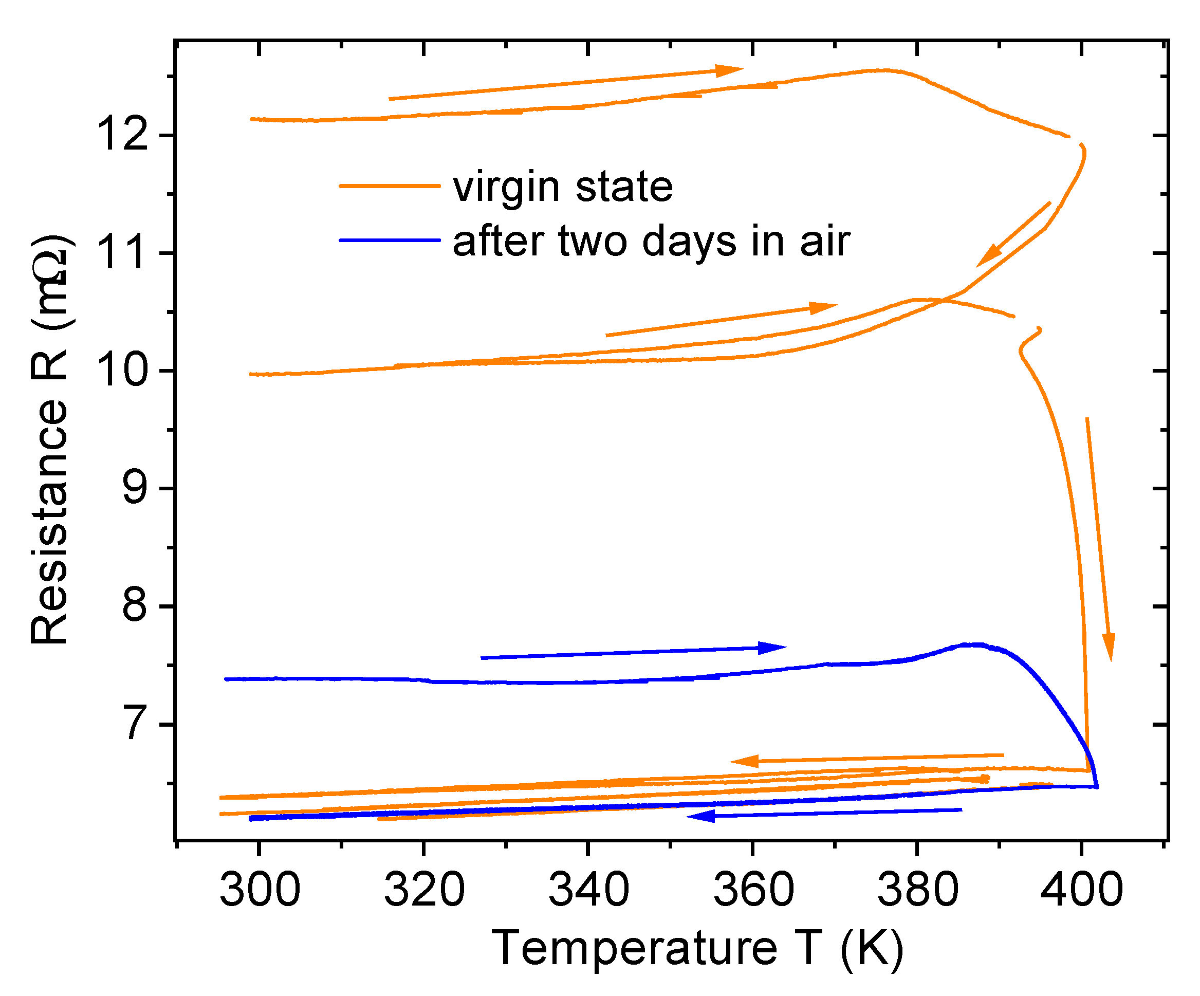
Figure 5.
Two independent measurements of the same HOPG sample #3 in the minicryo. The orange curve shows the temperature-dependent cycles of the sample starting just after the sample preparation in the virgin state. At the starting point of the cycles, the resistance at 300 K of this sample was 12.1 m decreasing to 6.2 m at the end of cycles at the same temperature. Afterwards, the sample was left for two days in air at normal conditions. After this time, the resistance of the sample was measured again with one temperature cycle as show by the blue curve.


Table 1.
Origin and dimensions of the measured samples. HOPG: Highly oriented pyrolytic graphite. Further characteristics of the internal structure of the HOPG sample, in particular TEM images, were reported in [7,8,26,29] and of the natural graphite sample in [9].
| Sample | Origin | Dimensions (mm) |
|---|---|---|
| #1 | HOPG-Advanced Ceramics | 4.63 × 1.3 × 0.47 |
| #2 | Natural Graphite-Sri Lanka | 3.2 × 0.5 × 0.14 |
| #3 | HOPG-Advanced Ceramics | 4.4 × 1.28 × 0.35 |
© 2020 by the authors. Licensee MDPI, Basel, Switzerland. This article is an open access article distributed under the terms and conditions of the Creative Commons Attribution (CC BY) license (http://creativecommons.org/licenses/by/4.0/).
Share and Cite
MDPI and ACS Style
Hentrich, A.; Esquinazi, P.D. Effects of the Stacking Faults on the Electrical Resistance of Highly Ordered Graphite Bulk Samples. C 2020, 6, 49. https://0-doi-org.brum.beds.ac.uk/10.3390/c6030049
AMA Style
Hentrich A, Esquinazi PD. Effects of the Stacking Faults on the Electrical Resistance of Highly Ordered Graphite Bulk Samples. C. 2020; 6(3):49. https://0-doi-org.brum.beds.ac.uk/10.3390/c6030049
Chicago/Turabian StyleHentrich, Andreas, and Pablo D. Esquinazi. 2020. "Effects of the Stacking Faults on the Electrical Resistance of Highly Ordered Graphite Bulk Samples" C 6, no. 3: 49. https://0-doi-org.brum.beds.ac.uk/10.3390/c6030049
Note that from the first issue of 2016, this journal uses article numbers instead of page numbers. See further details here.