Wideband Radar Absorbing Structure Using Polyaniline-Graphene Nanocomposite

Microwave Materials Research Laboratory, Department of Electronics, Cochin University of Science and Technology, Kochi 682022, India
*
Author to whom correspondence should be addressed.
C 2020, 6(4), 72; https://0-doi-org.brum.beds.ac.uk/10.3390/c6040072
Submission received: 4 October 2020
/
Revised: 26 October 2020
/
Accepted: 2 November 2020
/
Published: 5 November 2020
(This article belongs to the Special Issue Carbon Based Films: Characterization, Radiofrequency and Terahertz Applications)
Abstract
:A wideband non-resonant absorber is proposed, and its radar cross section (RCS) reduction is investigated. A discussion on the functional materials available is followed by the design of an absorber on a Plexiglas substrate with polyaniline-graphene nanocomposite as layered square inclusions with thicknesses and conductivities scaled to golden ratio. The measured dielectric properties of polyaniline-graphene nanocomposites are used in the fullwave simulation. The design parameters have been identified and optimized using CST Microwave Studio. As designed structure is fabricated and the reflection is measured. The objective of the work is to demonstrate the use of non-metallic conducting polymer composites devoid of metals for radar absorbing material (RAM) structural designs. The structure is an all-polymer and electrically thin design with a potential to be 3D printed to suit the target object.
1. Introduction
Radar-absorbing materials (RAM) are electromagnetic structures used to absorb the incident electromagnetic waves so that the reflected power as well as the transmitted power are reduced to a great extent [1,2]. Some of its applications such as radar cross section (RCS) reduction [3], electromagnetic interference (EMI) shielding [4], stealth technology [5] etc. in contemporary times are more demanding, in the sense of reduced thickness [6], wide bandwidth [7], polarization insensitiveness [8,9], and ease of fabrication [10,11], in such a way that traditional Salisbury screen [12] and Jaumann absorbers [13] are set aside. Another promising method for the design of RAM is the circuit analog absorbers wherein conductors are patterned above the ground plane so that the combination acts as a high impedance ground plane (HIGP), which creates a magnetic wall and hence the maximum electric field intensity at a much lower thickness than quarter wavelength of the frequency of interest [14]. Lumped resistances or patterned resistive films are used to dissipate the resonating microwave energy in the patches [11]. In a similar fashion, there are capacitive circuit absorbers employing low pass square resistive patches instead of bandstop frequency selective surface (FSS) resonators as that in circuit analog absorbers [15]. Both these techniques have resonant structures and require extensive optimizations and parameter analysis for achieving wideband nature for a higher wavelength to thickness ratio. They might need spacers which can lead to structural complexities that defy the very purpose of RCS reduction in core applications. The research in the field of 3D printable absorbers is a necessity when RCS from structures having complex geometries are to be reduced, which is getting attention in recent times particularly due to advancements in the additive manufacturing technology [16] and the advent of microwave materials with better absorption properties [17,18,19,20].
It is typical of resonant absorbers to have narrow bandwidth. Wide bandwidth resonant absorbers are realized by merging multiple narrowband resonant absorption. A non-resonant absorber, instead, is an impedance transformer which guides the incident wave and attenuates it while it is being guided, by virtue of electric and/or magnetic losses. Being a non-resonant method, the method is intrinsically broadband leading to wideband absorption. In this paper, the absorber is realized with non resonant technique, guiding the incident energy by impedance transformation from freespace to the metallic ground of the target. The absorber is an all polymer first iteration sierpinski fractal structure without resonating metal patches. It uses graded conductivity polyaniline-graphene composite embedded in a plexiglas substrate to effectively guide the incident wave and attenuate the field as it traverses through the material. The current work first discusses engineering aspects related to the feasible implementation of non-metallic conducting composites for RCS reduction. Second, it extends our previous work on PANi-graphene composite to the proposed RAM structural design and its performance analysis so as to demonstrate the use of non-metallic conducting polymer composites devoid of metals, which is the objective of this work.
2. Choice of Conducting Polymers
Conducting polymers comprise a long chain of carbonaceous materials which are formed by polymerization reaction of its monomers under optimum reaction conditions [21]. They are non-metallic yet electrically conducting materials whose conductivity can be tuned to suit the required material properties. A few examples of these are Polyacetylene, Polypyrrole, Polyaniline, Polythiophene, etc. Each of these materials has its own niche of physical properties [22]. Some of these properties include tunable/reversible conductivity via doping/dedoping process [23], tunable optical properties [24], thermoelectric activity [25], environmental parameter sensing [26], etc. Out of all these examples, Polyaniline (PANi) has the advantages of environmental stability and availability of cheap monomers, and therefore many applications propose PANi as a promising candidate. The importance and potential use of PANi in electronics is a broad subject in which microwave applications such as EMI shielding, wearable antenna applications do come often as the stakes are high for a flexible high conductive non-metallic material and it is no wonder that quite a large number of material research groups have done impressive contributions in this field [27,28,29,30]. Yet there exists a practical non-viability in the real-world applications of these wonder polymers in microwave. This arises mainly due to the inverse relation between the conductivity of these polymers and their large-scale processibility.
Conducting polymers, which are obtained as powder precipitates in typical reactions, are inherently composed of core shells with metallic conductivity immersed in a pool of dielectric. The chain structure of these polymers are readily conducting entities with a very high intra-chain conductivity in their doped state. However, when considering their inter chain or inter domain electron transport, they have a finite charge tunneling probability and the bulk conductivity is greatly reduced. The conductivity can of course be enhanced by various techniques starting from its altered synthesis routes, secondary doping, mixing with other conducting polymers and stable dispersions in solvents. When a film form of the material is sought, dispersions of PANi in solvents like N-methyl-2-Pyrrolidone, m-cresol, Triton X is made which can be coated onto substrates by spray coating/spin coating/dip coating techniques [31,32]. These solvents are said to interact with the polymer backbone under the influence of certain dopants based on sulphonic acids, giving rise to conformational stretching or uncoiling of polymer chains so that long-range electron transport improves with a high crystallinity in the bulk material [33]. Highly conducting PANi films are therefore obtained by such methods whose microwave properties are of great interest as they can act as conductive patches in flexible antennas. However, these films need not be a free standing one or the films might deteriorate with ambient conditions and thus practical applications are limited to wafer fabrication, for instance, in sensor applications. If a flexible thick sheet form is required, then PANi can be dispersed in any of the above organic solvents along with conventional polymers such as Natural rubber, Polymethyl methacrylate (PMMA), Polyvinyl chloride (PVC), or Polyethylene terephthalate (PET) and cast into thick sheets [34,35]. There is an innate loss of conductivity in these blended composites as the matrix polymer hinders charge transport. From an electromagnetic point of view, these composites can be modeled as lossy dielectrics rather than as lossy metals. A yet another approach in making high quality conducting polymer films is by plasma polymerization [36]. For this, the size of the substrate should be very small and is not suitable for RAM/FSS applications albeit their untapped potential in millimeter waves as substrate integrated waveguides and leaky wave structures.
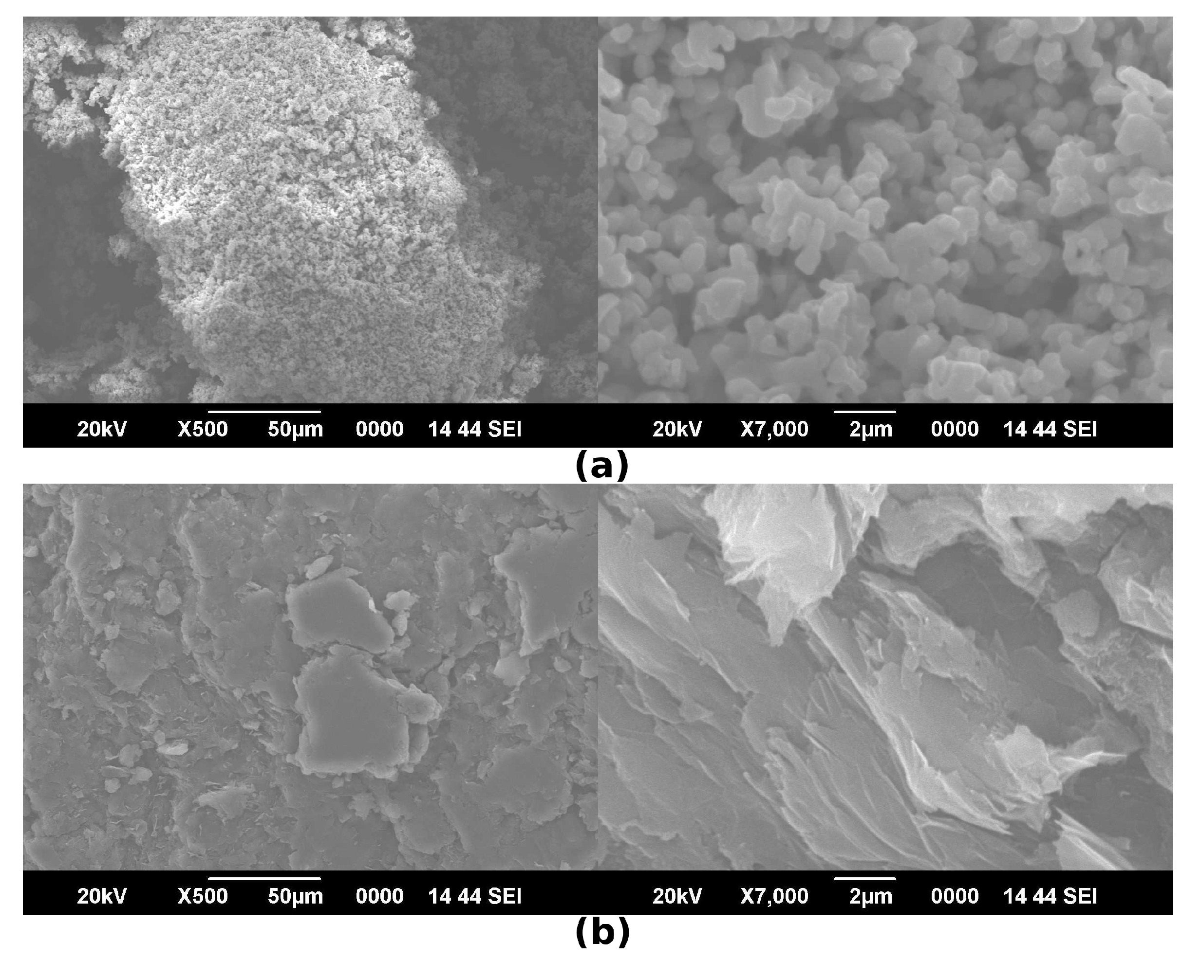
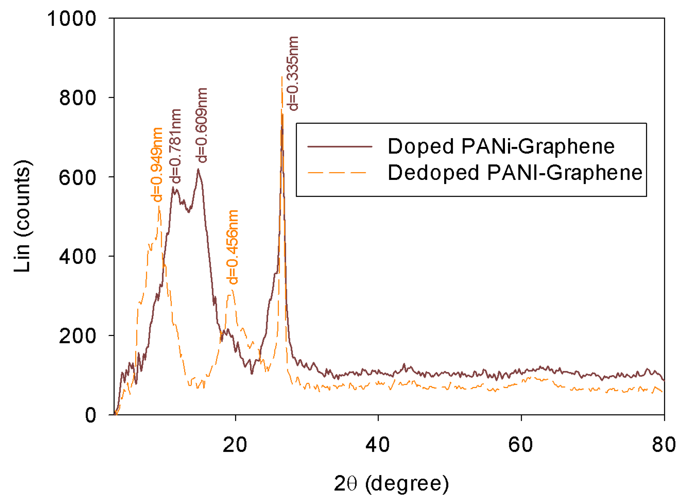
In all these preparations, it is highly unlikely to obtain laboratory conductivities during large scale processing in bulk of these polymers. One method to increase the bulk conductivity is by adding conductive fillers like metal nanopowders or carbon nanotubes or graphene or any other conducting polymer of interest [37,38,39]. This is done by ex-situ or in-situ methods. The first method involves mechanical milling and mixing of the selected conducting filler in the already conducting host matrix. The ratio of the filler to host determines the final product conductivity. The second method is to polymerize the monomers in the presence of fillers. This method has significant impact on conductivity as the material is blended with its filler at a molecular level. A comparison of the Scanning electron microscopy (SEM) images of exfoliated graphene and PANi-graphene nanocomposite prepared via the route specified is shown in Figure 1. The images in the bottom portion represent the exfoliated graphene layers. The images on the top are graphene after PANi polymerization where it can be seen that the sheets are now covered in coral-like nanostructured PANi. The fillers need to act as nucleation sites for the monomers to start reacting into polymers. In the case of polyaniline-graphene composite, polyaniline needs a lower pH medium to polymerize, whereas graphene needs a high pH medium. At a lower pH, the graphene layers tend to agglomerate and readily sediments into the bottom of the reaction medium. In standard procedure, graphene is oxidized into graphene oxide, which is stable in low pH and then the PANi monomers are allowed to polymerize on them [40,41]. This has a downside that, graphene oxide is not a good conductor. So these procedures are eventually followed by a reduction reaction which removes the -OH groups using hydrazine or microwave irradiation or by UV laser, getting back to a reduced graphene oxide form. In the process, the crystallinity of graphene layers is somewhat distorted which is more commonly referred to as wrinkles in graphene sheet. These distortions can be avoided by using graphene as such with the help of dispersion stabilizers or surfactants. Therefore, a dispersion stabilizer like Polystyrene sulphonate (PSS) or Gelatin needs to be used so that the polymerization can proceed on these well dispersed graphene templates. To add to this stability provided by stabilizers, as the polymerization commences, the interaction of PANi reacting species with graphene also results in dispersion stability. The X-ray diffraction (XRD) spectrum of conducting polymers can give insight into the inherent structural peculiarities and defects which alter charge transport in these materials. As PANi is a conducting polymer whose doping can be reversed so that a highly conducting sample can be de-doped to form insulating state reversibly, a composite of PANi with graphene exhibits a reversible conductivity depending on doping state (i.e., doped and de-doped states). The quality of the PANi-graphene composite is evident from the X-ray diffraction (Figure 2) as the product retains the sharp crystalline peaks of graphene at 2 = 26.521. The presence of doped PANi salt is confirmed by 2 = 14.898. It is to be noted that in the PANi-graphene composite, the crystalline peak corresponding to graphene layers do have a reduction in interplanar distance from d = 0.338 nm to d = 0.336 nm after the polymerization. This is an indication of the interaction of intercalated PANi with the graphene layers thereby reducing the width of the potential wall existing between graphene sheets in the off-plane direction. There can be chances of oxidation of exfoliated graphite during the polymerization reaction. This is an unsought side reaction of the radical initiator such as potassium permanganate or ammonium peroxodisulphate (APS) used to start PANi polymerization. The peak at 2 = 11.508 corresponding to the GO has a broader width due to its interaction with PANi resulting in a significant reduction in interplanar spacing from d = 0.838 nm to d = 0.781 nm. These effects result in the increase in conductivity of the composite in the off-plane direction of graphene sheet.
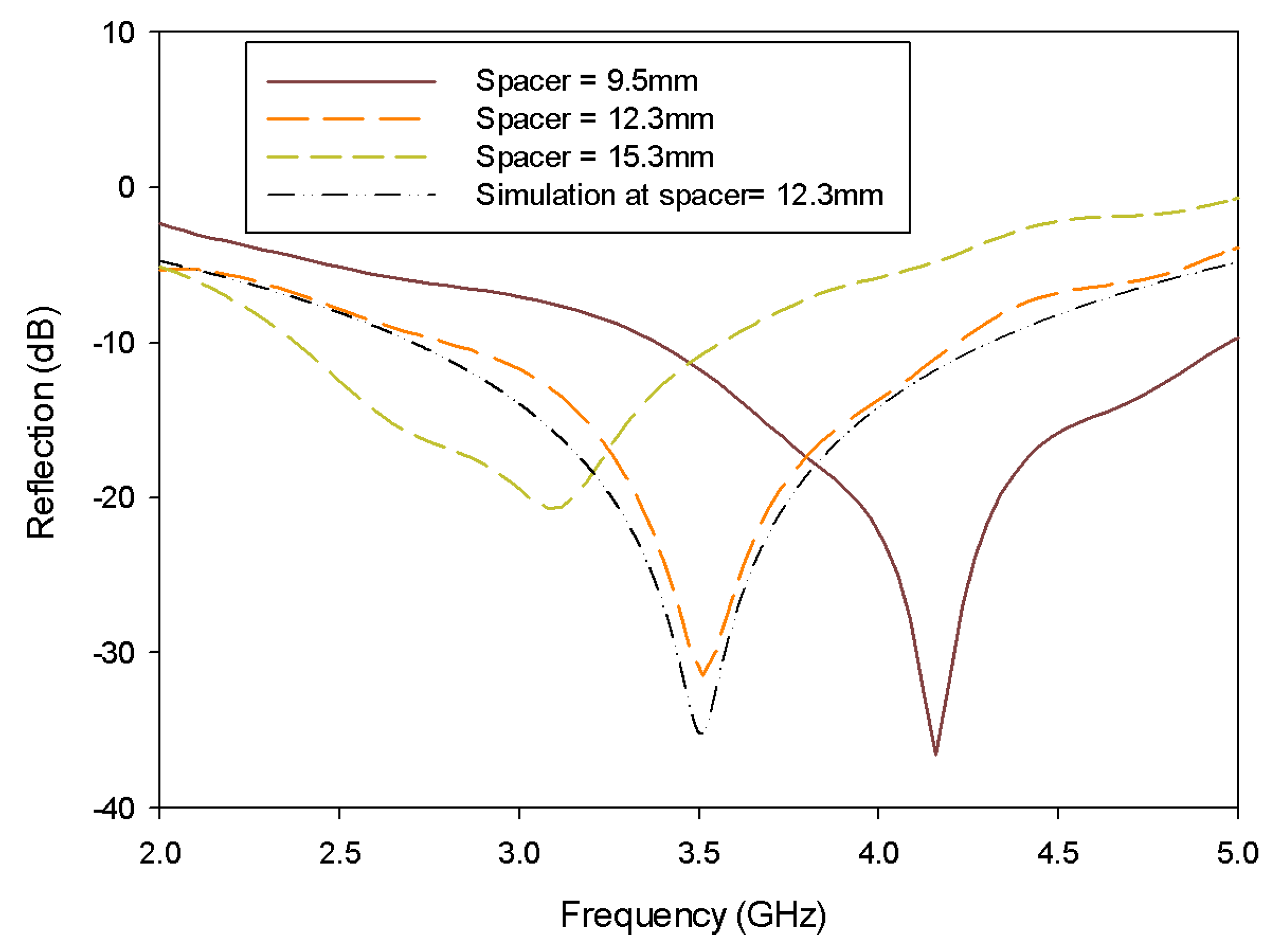
Graphene is a well acclaimed non-metallic conductor which has potential in bandgap and conductivity tuning. The hype around graphene is also followed by such difficulties in obtaining high-quality sheets with good mechanical strength at microwave length scales. High-quality graphene coatings are obtained on silica or quartz by chemical vapor deposition (CVD), but on a very small scale. Nevertheless graphene has a promising property of forming very thin stable sheets on certain substrates by mere application of shear stress [42]. This can be done to make ohmic sheets that can act as resistive sheets in Salisbury screens or patterned as resistive metasurfaces in circuit analog absorbers or in FSS. These coatings can be made very thin and conductive so that the real part of complex permittivity is seldom considered and the coating acts as a lossy metal. A Salisbury absorber utilizing microwave exfoliated sulfuric acid intercalated graphene as resistive coating with an average surface resistance of 390 /square over a Plexiglas substrate (dielectric constant = 3.02 as measured using NRW algorithm) is fabricated at our facility and its measured reflected power for normal incidence is indicated in the Figure 3 for demonstration purpose. Three spacer thicknesses were used and the corresponding resonance shifts in the absorption peaks are clearly observable from the figure. Other complex shapes can be made by laser patterning technique. This demonstration indicates the prospects of non-metallic conductors with their tunable intrinsic properties and their constitutive parameters that suit them for microwave applications. Additionally, such all-polymer designs have high demand in additive manufacturing for microwave technology. Conducting polymers can be blended with other host matrix polymers, which then can be 3D printed either by photopolymerization, material jetting, extrusion, or by any method to break the limits of fabrication [16].
3. Design of the Proposed Wideband Non-Resonant Absorber
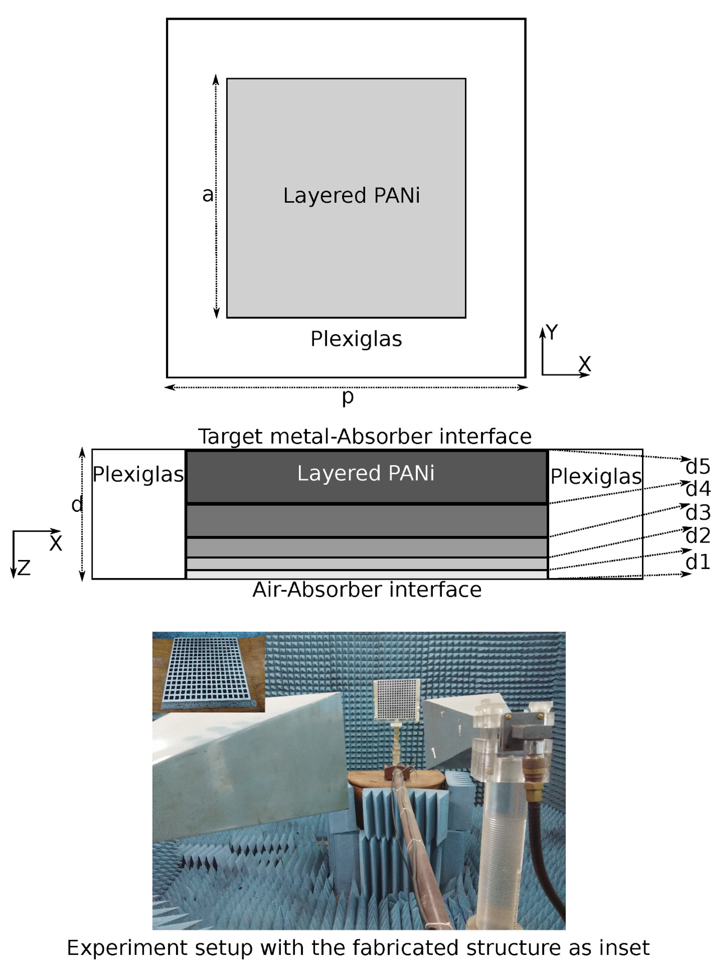
In this section, a design schema for the all-polymer microwave absorber is outlined. Recent findings reveal the conducting polymer-poly(3,4-ethylenedioxythiophene) polystyrene sulfonate (PEDOT:PSS) as a promising candidate for microwave applications [43,44,45]. However, its RAM applications, which require it in higher quantities, are limited by the enormous manufacturing cost involved when compared to PANi. In a microwave scale of physical lengths, compressed pellet forms of PANi-graphene nanocomposites offer moderate conductivity and good physical strength at a much lower cost. Therefore, the shortcomings of the PEDOT:PSS can be overcome by using PANi in combination with graphene. A typical synthesis routine for the preparation of PANi-graphene composite in a gelatin stabilized media from aniline and microwave-assisted exfoliated graphite, and its dielectric characterization are detailed in our previous work [46]. The conductivity modulation can be done using proper acid (for doping) or base (for dedoping) in a controlled nitrogen environment by introducing vapour phase dopants at predetermined concentrations to the powder form of PANi-graphene composites. Thus, PANi-graphene composites with graded conductivities can be obtained. These powders can be compressed to make a conductivity graded pellet. Their thicknesses can be adjusted using PCB milling system. In the current design, a Plexiglas substrate is chosen as it is transparent and easy to 3D print or etch out unwanted regions by instant vaporization using concentrated laser power without burn-in effects. The substrate thickness is mm with a dielectric constant of 3.6 and electrical conductivity of 0.02 Sm. Periodic sierpinski first iteration squares can be etched out from the substrate into which conductivity graded 5 layered square shaped PANi-graphene pellets are inserted as inclusions. The conductivity of each adjacent layer of the composite varies in the golden ratio with the air interface layer having lowest conductivity and the target interface layer having the highest conductivity. Similarly, the ratio of thickness of each adjacent layer is also chosen to be of the golden ratio with the air interface layer being the thinnest. The thickness and conductivity of the layers can be expressed as the following vectors.
Thickness,
Conductivity,
where mm and Sm are scalar parameters estimated by Trust Region optimization algorithm of CST microwave studio and the constants of the right hand side are scaling factors from Fibonacci series, where the ratio of adjacent elements is the golden ratio. The rationale behind the selection of golden ratio is that many naturally occuring and human-made systems have logarithmic structures obtained from designs implementing golden ratio [47,48]. Therefore, this ratio has an innate non-resonant nature. Golden ratio and Fibonacci series are used in computational problems [49], stock market predictions [50], fractal structures [51], etc. The indexes 1 to 5 represent layers from top to bottom.
The final structure is depicted in Figure 4. The width of the patch mm and the periodicity mm are optimized to suit the design requirements.
4. Results and Discussion
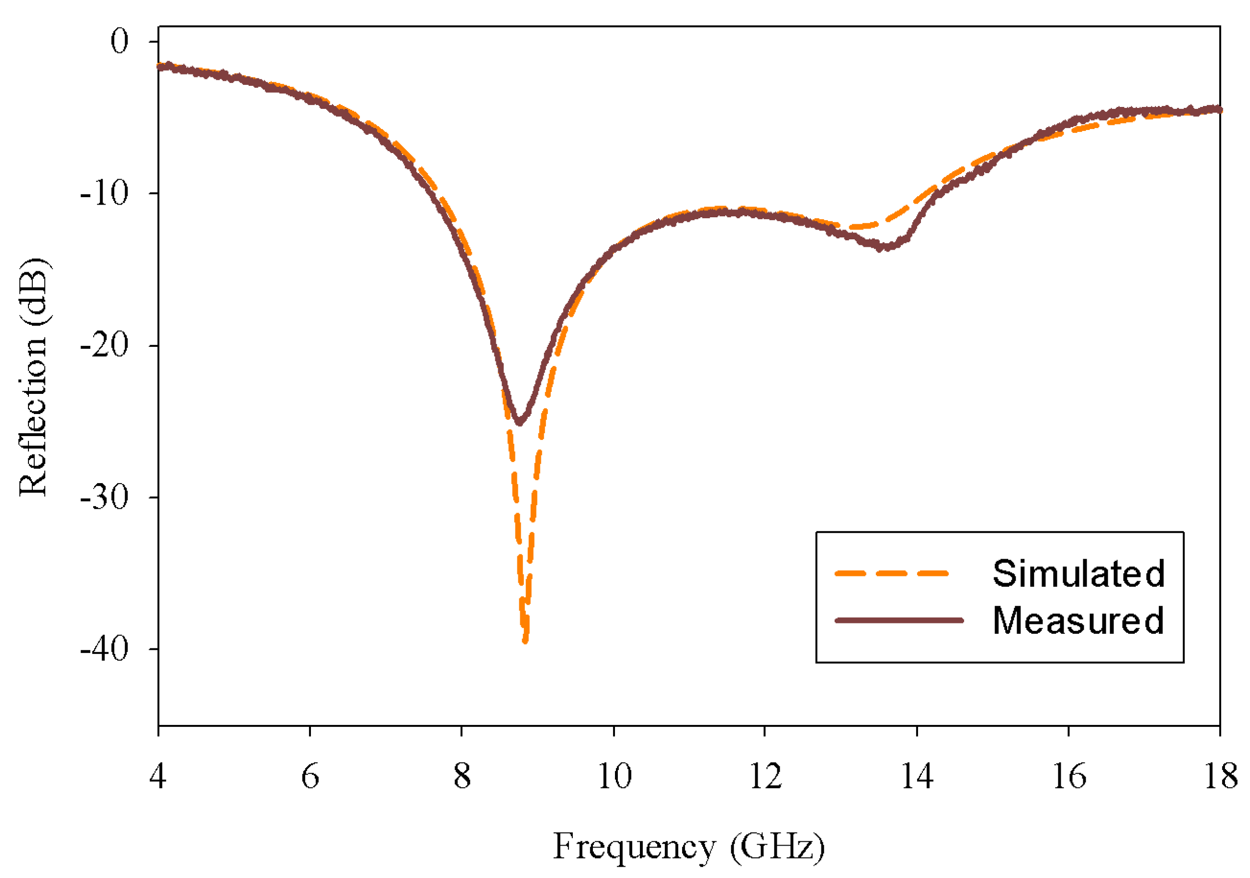
The unit cell of the absorber was modeled and optimized in CST microwave studio. The structure is fabricated out of the same unit cell with elements on a Plexiglas substrate of size mm × mm as shown in Figure 4. Polyaniline-graphene pellets are conductivity tuned in a controlled nitrogen atmosphere using Camphor Sulphonic Acid (CSA) as dopant. The square holes are made in the substrate using laser patterning and the pellets are inserted in the square holes. The reflection is measured in freespace using wideband horn antennas connected to Rohde and Schwarz ZVB20 Vector Network Analyzer calibrated with metal plate of same dimension as that of the test structure in fully shielded anechoic chamber. The reflection (Figure 5) shows a 10 dB reduction ranging between 7.8 GHz and 14 GHz, as measured. It can be seen that the measured curve is similar to that of the full EM simulated results from CST Microwave studio although it registers some slight variations from simulation. This can be attributed to the fabrication irregularities involved in the prototype. As defined elsewhere [18], the parameter in this case is found to be 4.27, where . The structure thickness in terms of multiple of wavelength is listed for comparison for different recent designs in Table 1. The mode to mode coupling is a measure of how much of the incident power in one particular mode has been converted to another mode after reflection. If the incident power in the transverse electric (TE) mode has been converted to transverse magnetic (TM) mode upon reflection from the surface, the mode to mode coupling between incident TE mode and reflected TM mode would be significantly high. This is a case of polarization rotated reflection and cannot be considered as wave absorption. A proper absorber should have a very low mode to mode coupling over the band of operation. The mode to mode couplings (Figure 6) indicate that the phenomenon is absorptive and it is not a case of polarization rotated reflection as the mode to mode coupling for the bandwidth is lower than −80 dB.
4.1. Parametrics
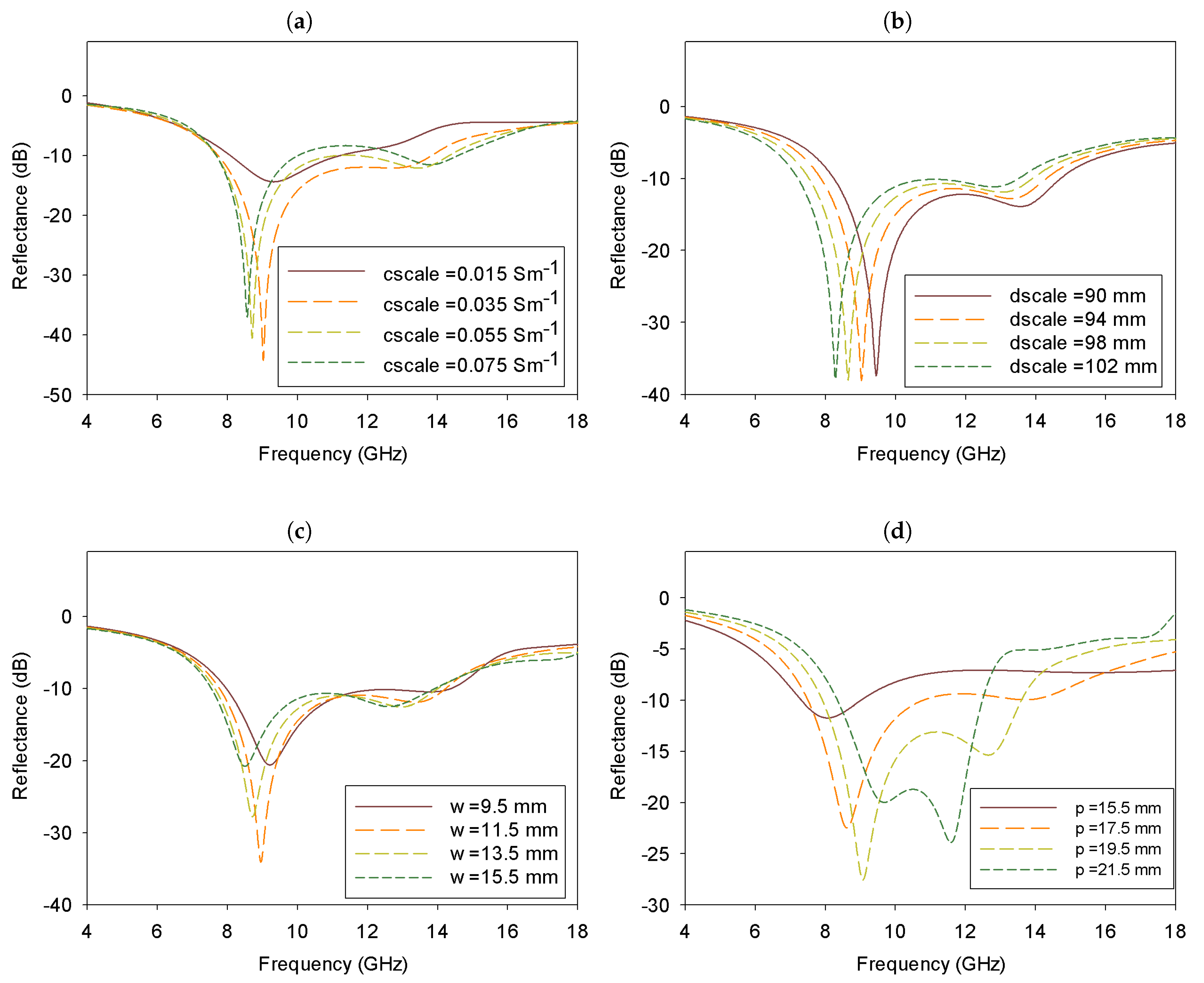
It is found that, rather than a dependence on the width of the resistive square as that in the case of circuit analog absorbers, the band of operation is significantly determined by the thickness of the structure manifested in the factor “dscale” (Figure 7b). There exists a dependence of band of operation and matching on parameters cscale, w, and p as shown in Figure 7a,c,d, respectively. Any increase in the width and the spacing of the square patch beyond half wavelength results in the entire structure becoming an electromagnetic scatterer for higher frequencies in the operating band. It can be inferred that the absorption mechanism is due to resonance of the structure thickness at lower frequencies and due to edge diffraction at higher frequencies.
4.2. Angular Variation
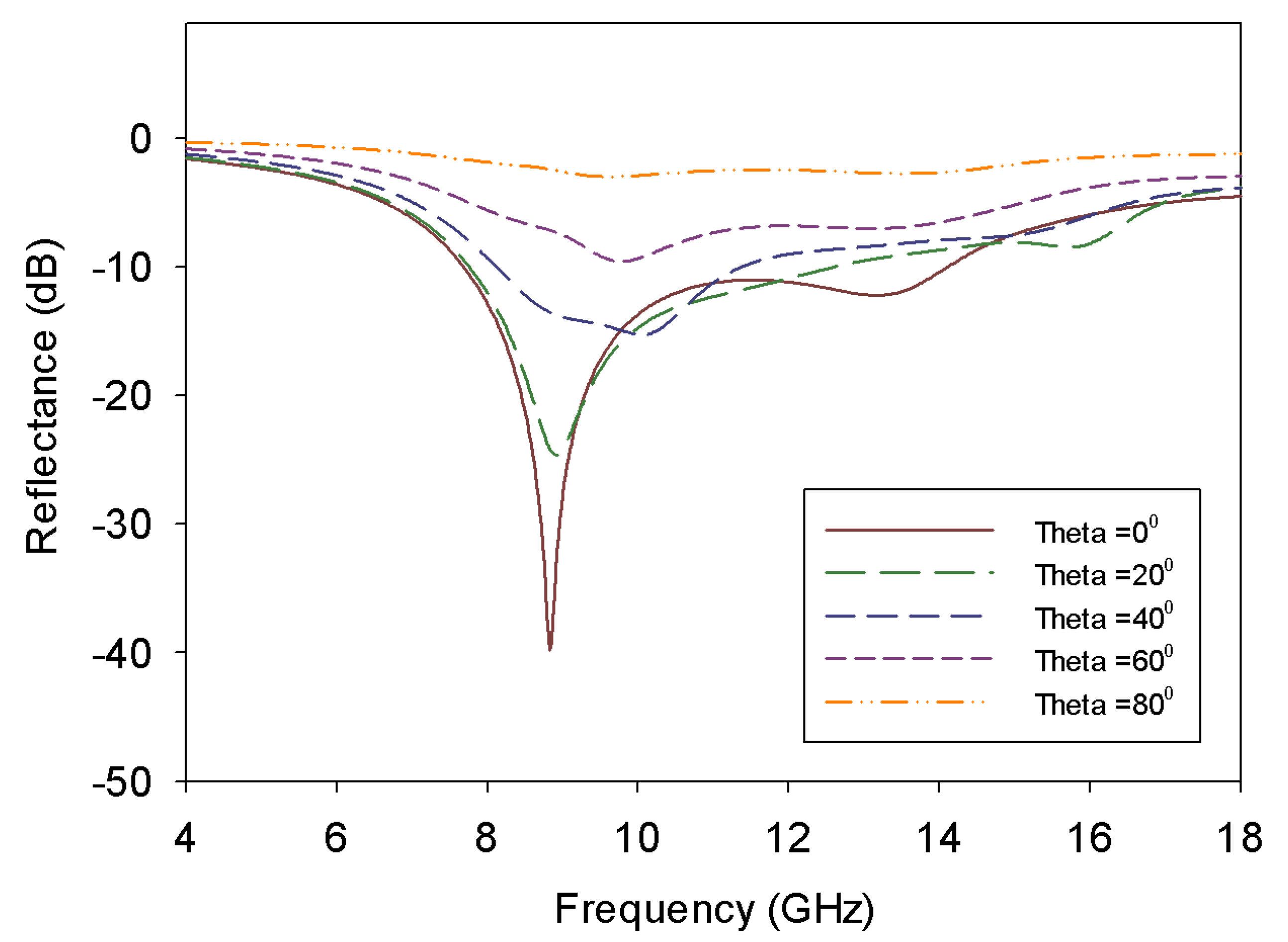
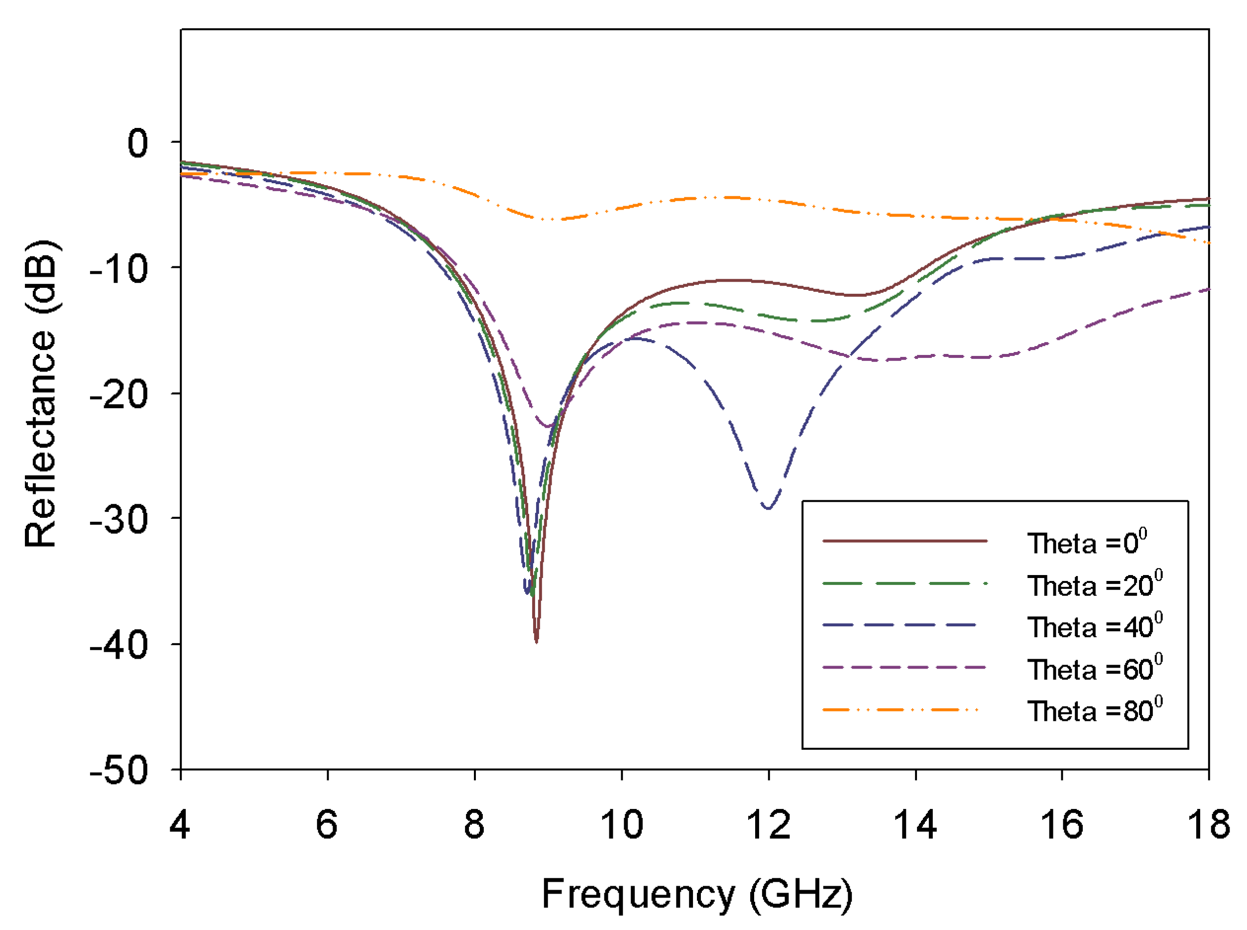
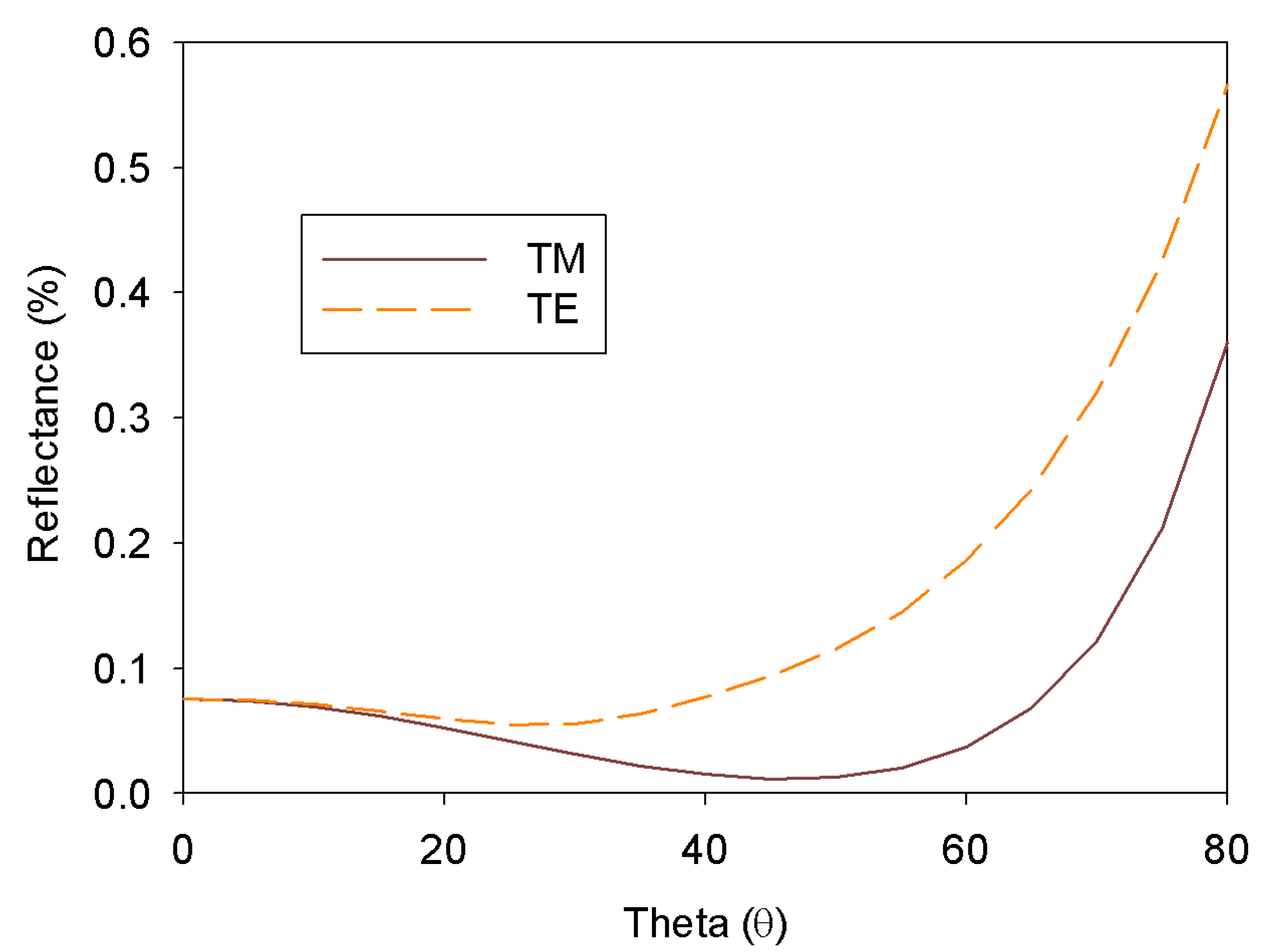
Due to the fourfold rotation symmetry of the structure, both TE and TM polarizations have the same response upon normal incidence. As evident from Figure 8, the angular variation of reflected power for TE mode satisfies a variation upto 30 incident angle after which the response deteriorates within X band. With the angular variation, the TE mode absorption deteriorates whereas the TM mode (Figure 9) shows good absorption at wider angles. This is to be expected as the coupling of TM modes are different from that of TE at oblique angles of incidence. In graded non-resonant absorbers, the TM modes refract into the medium which gives rise to the wideband absorption of those modes at oblique angle of incidence. There exists an angle of incidence at each frequency for which the reflection is minimum in the case of TM modes. This is typical of lossy dielectrics and this angle of incidence is called the Pseudo Brewster angle for the composite structure [54,55]. The variation of reflectance with angle of incidence for both TE and TM at 11 GHz from the Figure 10 indicates the standard lossy dielectric behavior. This is not seen in TE modes as their absorption continues to deteriorate with obliqueness. From the Figure 10, the Pseudo Brewster angle for the structure is found to be 46.5.
4.3. Field Distribution and Power Loss
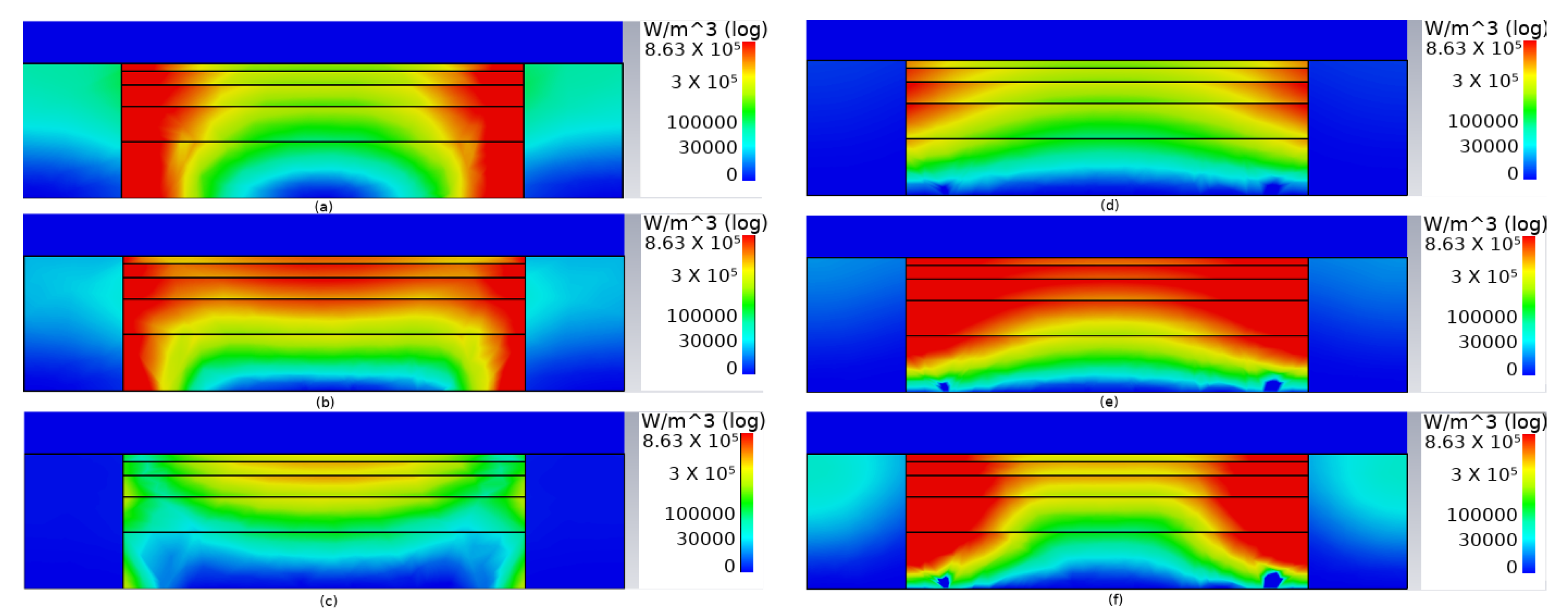
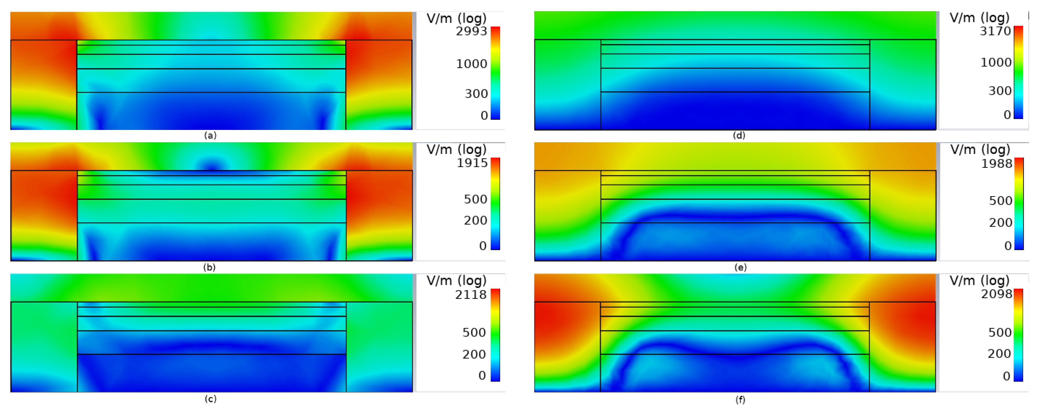
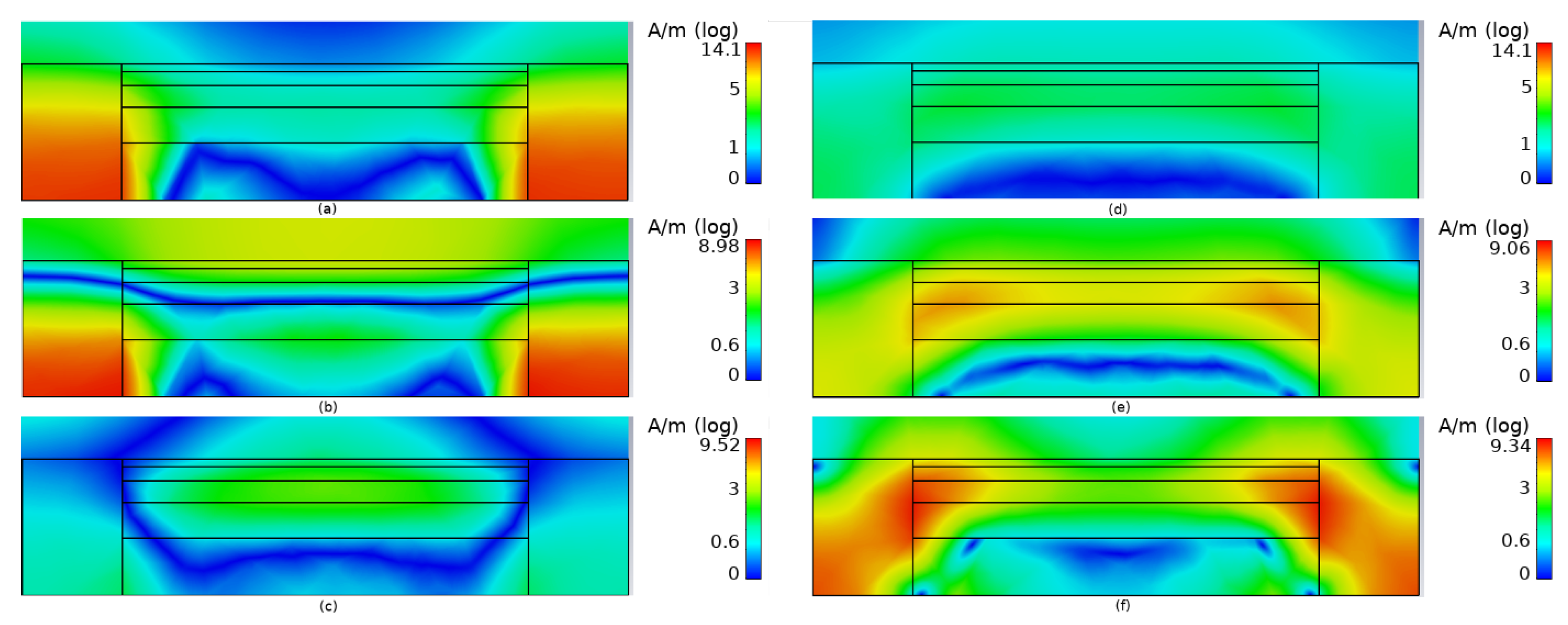
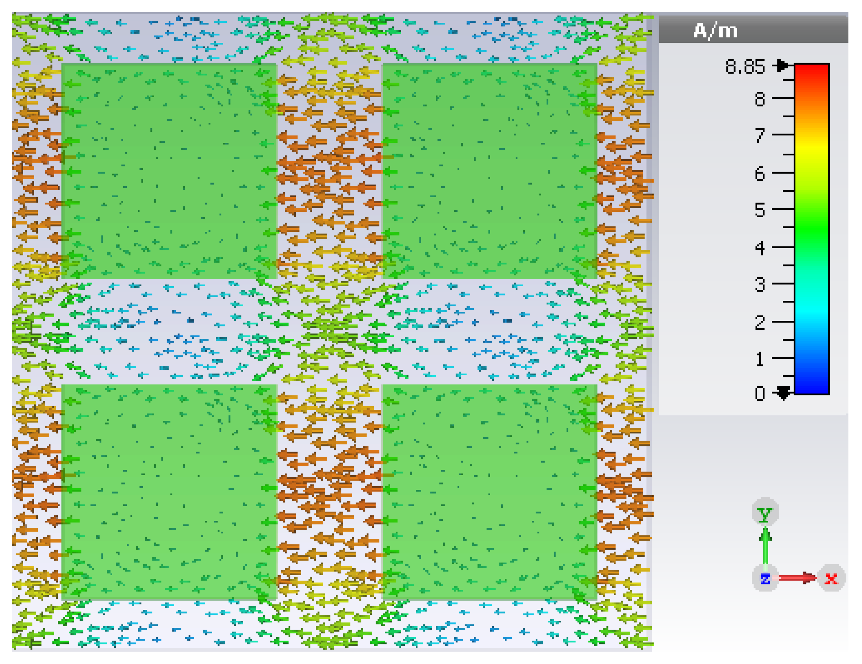
The power loss density distribution in the structure as shown in Figure 11 indicates the strong coupling of incident waves into the structure. It can be seen in the structure that significant power loss happens in PANi as compared to the surrounding Plexiglas substrate. The incident power is heavily dissipated in the top layers and there exists a loss gradient from top to bottom inside the pellet as is indicative from the figure. It is also found that a power loss gradient exists in each layer, which is very high at the edges of the PANi pellet when compared to the central regions. This has a strong dependence on the polarization of incident wave. The PANi-Plexiglas edges where the electric fields are found to be normal exerts high power loss compared to the perpendicular edge. It can be seen that the loss is slightly higher just below the interface between two PANi layers than that it is just above the interface. This effect is due to the fact that any adjacent bottom layer is having a higher conductivity than the top layer. Hence the ohmic loss encountered by the field will be slightly more in the bottom layer near the interface than above the interface. The electric and magnetic field distributions are shown in the Figure 12 and Figure 13, respectively, which shows that there exist a region near the metal where both electric and magnetic fields exists at their minimal value. This is due to the decrease in electric field amplitude as the field attenuates in the pellet gradually. As the field traverses through the pellet, it is subjected to electric losses which is more in the central portion of the pellet hence the surface currents generated on the ground is minimal below the pellet than that it is at the metal under Plexiglas region. The magnetic field strength is high under the lossless portion of the absorber. As shown in the Figure 14, this creates a periodic current pattern with constant phase in the ground.
4.4. Bistatic RCS Analysis
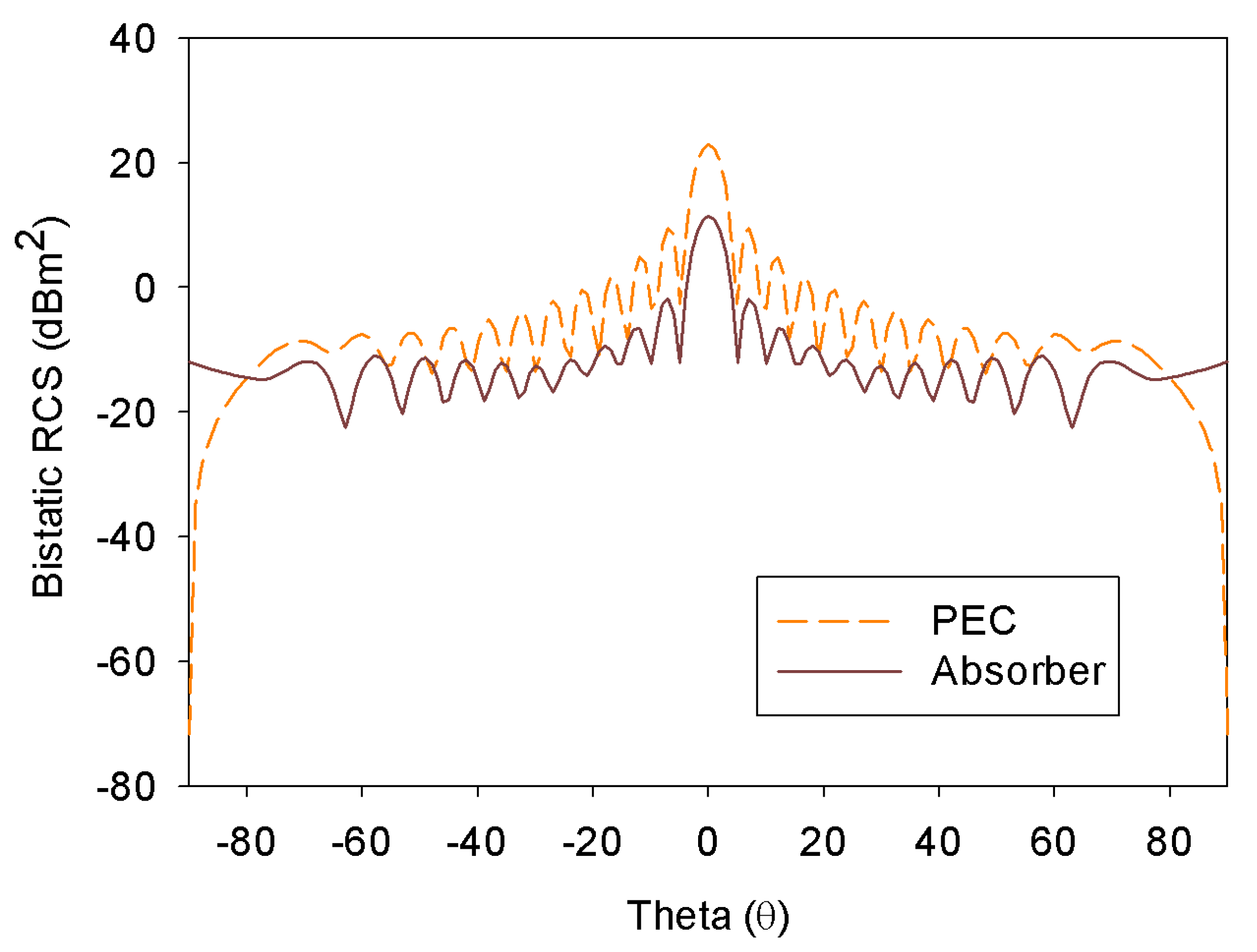
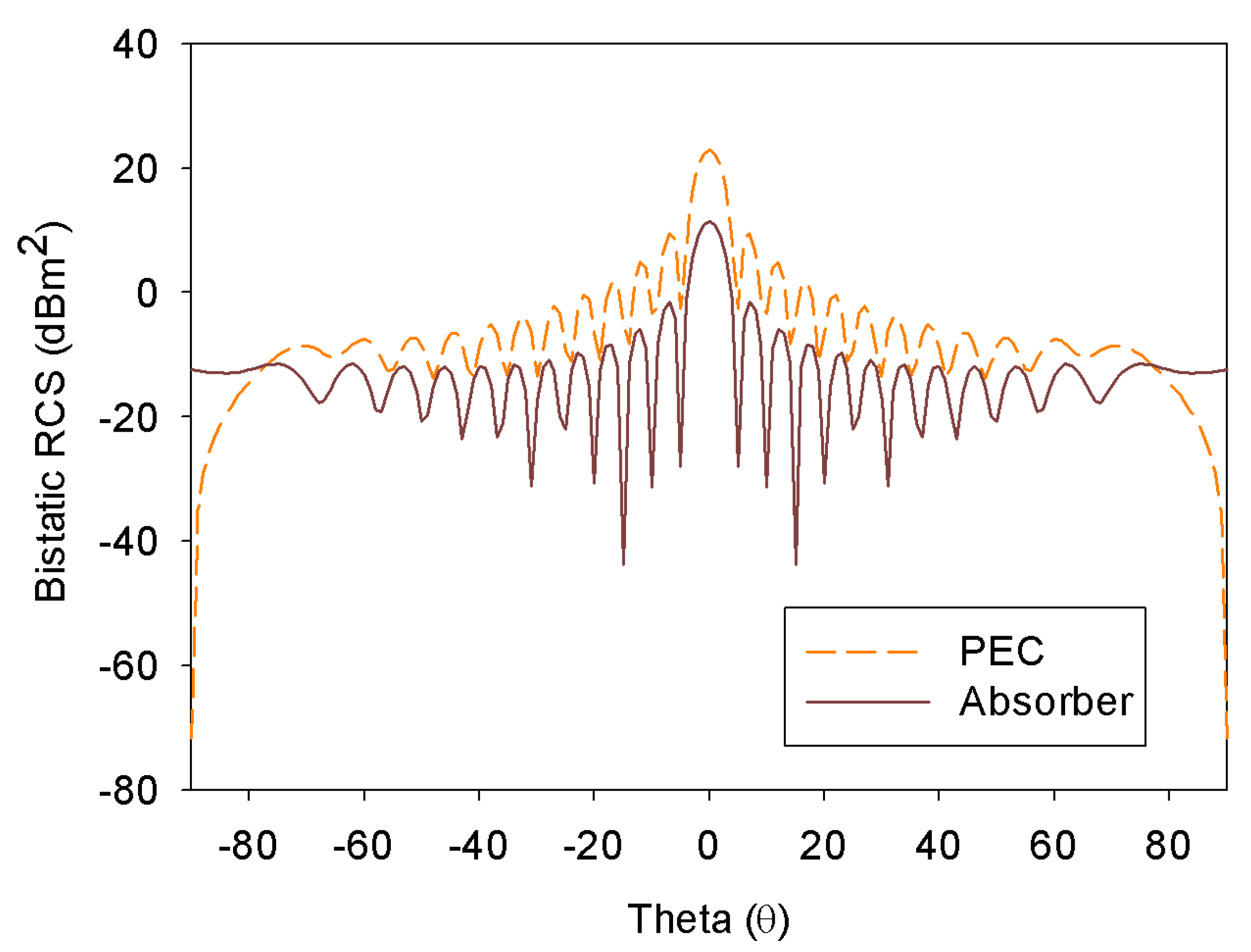
The RCS reduction in main lobe is about 11.42 dB. Both vertical polarization (theta = 0, phi = 0) and horizontal polarization (theta = 0, phi = 90) for the center frequency (11 GHz) have been plotted in Figure 15 and Figure 16. It can be seen that at theta = , the PEC has a very low RCS, whereas the absorber shows more RCS compared to PEC which can be attributed to evanescent waves propagating along the target metal–absorber interface. In practical applications, this mode can be seldom considered as it is parallel to the absorber. At all the frequencies in the band, the main lobe power is reduced by absorption mechanism as there is no increase in side lobe power or cross polar power which indicates the absence of scattering.
5. Conclusions
An all-polymer non-resonant wideband absorber with a potential of 3D printing is designed and fabricated. The structure, made of Plexiglas, contains PANi-Graphene composite with graded conductivity which acts as an impedance transformer to guide the incident electromagnetic fields and attenuate them. The five-layered PANi pellet has graded conductivity and thickness based on golden ratio. The parameters have been optimized and the structure absorbs X band and the lower part of Ku band. Its material and microwave absorptive characteristics have been quantified in terms of SEM analysis, XRD analysis, reflection loss, bistatic RCS, angular stability and power loss density, and field distribution. The proposed design strategy offers two advantages over conventional methods: The first advantage of the all-polymer absorber design specified here is in the weight reduction that is achieved. As metals are not used in these designs, the weight of entire structure is dependent on the polymer which is light weight in comparison, reducing the fuel requirements while simultaneously reducing the RCS of the entire system in the case of moving targets. The second advantage of such polymer-based structures is in the facile additive manufacturing technology that can aid in rapid generation of complex shapes to suit the target geometry.
Author Contributions
Conceptualization, P.T.; Data curation, A.C.K.; Formal analysis, P.T. and N.K.P.; Funding acquisition, A.C.K.; Investigation, P.T., L.V.A., and N.K.P.; Methodology, P.T., L.V.A., N.K.P., and A.C.K.; Project administration, A.C.K.; Resources, N.K.P. and A.C.K.; Software, P.T. and A.C.K.; Supervision, A.C.K.; Validation, P.T., L.V.A., N.K.P., and A.C.K.; Visualization, P.T.; Writing—original draft, P.T.; Writing—review and editing, N.K.P. and A.C.K. All authors have read and agreed to the published version of the manuscript.
Funding
This research received no external funding.
Acknowledgments
The authors acknowledge the assistance provided by UGC(SAP) and DST(FIST), Govt. of India. The material measurements facility provided by Sophisticated Test and Instrumentation Centre (STIC), India and the technical support in laser patterning the structure provided by SignPlus Digital Arts is also acknowledged.
Conflicts of Interest
The authors declare no conflict of interest.
References
- Emerson, W. Electromagnetic Wave Absorbers and Anechoic Chambers Through the Years. IEEE Trans. Antennas Propag. 1973, 21, 484–490. [Google Scholar] [CrossRef]
- Plyushch, A.; Macutkevic, J.; Svirskas, S.; Banys, J.; Plausinaitiene, V.; Bychanok, D.; Maksimenko, S.A.; Selskis, A.; Sokal, A.; Lapko, K.N.; et al. Silicon carbide/phosphate ceramics composite for electromagnetic shielding applications: Whiskers vs particles. Appl. Phys. Lett. 2019, 114, 183105. [Google Scholar] [CrossRef]
- Deng, R.; Li, M.; Muneer, B.; Zhu, Q.; Shi, Z.; Song, L.; Zhang, T. Theoretical analysis and design of ultrathin broadband optically transparent microwave metamaterial absorbers. Materials 2018, 11, 107. [Google Scholar] [CrossRef] [PubMed] [Green Version]
- Beeharry, T.; Yahiaoui, R.; Selemani, K.; Ouslimani, H. A dual layer broadband radar absorber to minimize electromagnetic interference in radomes. Sci. Rep. 2018, 8, 382. [Google Scholar] [CrossRef] [PubMed] [Green Version]
- Li, Y.; Huang, J.; Hong, S.; Wu, Z.; Liu, Z. A new assessment method for the comprehensive stealth performance of penetration aircrafts. Aerosp. Sci. Technol. 2011, 15, 511–518. [Google Scholar] [CrossRef]
- Theofano, M.K.; Alexandros, I.D.; Stylianos, D.A.; Nikolaos, V.K.; Christos, S.A. A family of ultra-thin, polarization-insensitive, multi-band, highly absorbing metamaterial structures. Prog. Electromagn. Res. 2013, 136, 579–594. [Google Scholar]
- Zabri, S.; Cahill, R.; Schuchinsky, A. Compact FSS absorber design using resistively loaded quadruple hexagonal loops for bandwidth enhancement. Electron. Lett 2015, 51, 162–164. [Google Scholar] [CrossRef] [Green Version]
- Minyeong, Y.; Hyung, K.K.; Sungjoon, L. Angular- and Polarization-Insensitive Metamaterial Absorber Using Subwavelength Unit Cell in Multilayer Technology. IEEE Antennas Wirel. Propag. Lett. 2016, 15, 414–417. [Google Scholar]
- Li, L.; Lv, Z. Ultra-wideband polarization-insensitive and wide-angle thin absorber based on resistive metasurfaces with three resonant modes. J. Appl. Phys 2017, 122, 055104. [Google Scholar] [CrossRef]
- Jiang, W.; Yan, L.; Ma, H.; Fan, Y.; Wang, J.; Feng, M.; Qu, S. Electromagnetic wave absorption and compressive behavior of a three-dimensional metamaterial absorber based on 3D printed honeycomb. Sci. Rep. 2018, 8, 4817. [Google Scholar] [CrossRef] [PubMed]
- Lu, Y.; Chi, B.; Liu, D.; Gao, S.; Gao, P.; Huang, Y.; Yang, J.; Yin, Z.; Deng, G. Wideband Metamaterial Absorbers Based on Conductive Plastic with Additive Manufacturing Technology. ACS Omega 2018, 3, 11144–11150. [Google Scholar] [CrossRef] [PubMed]
- Fante, R.; Mccormack, M. Reflection Properties of the Salisbury Screen. IEEE Trans. Antennas Propag. 1988, 36, 1443–1454. [Google Scholar] [CrossRef]
- Du Toit, L.J. The Design of Jauman Absorbers. IEEE Antennas Propag. Mag. 1994, 36, 17–25. [Google Scholar] [CrossRef]
- Munk, B.; Munk, P.; Pryor, J. On designing Jaumann and circuit analog absorbers (CA absorbers) for oblique angle of incidence. IEEE Trans. Antennas Propag. 2007, 55, 186–193. [Google Scholar] [CrossRef]
- Zadeh, A.; Karlsson, A. Capacitive circuit method for fast and efficient design of wideband radar absorbers. IEEE Trans. Antennas Propag. 2009, 57, 2307–2314. [Google Scholar] [CrossRef] [Green Version]
- Tan, L.J.; Zhu, W.; Zhou, K. Recent Progress on Polymer Materials for Additive Manufacturing. Adv. Funct. Mater. 2020, 30, 2003062. [Google Scholar] [CrossRef]
- Meisak, D.; Gurnevich, E.; Plyushch, A.; Bychanok, D.; Georgiev, V.; Kotsilkova, R.; Kuzhir, P. Robust design of compact microwave absorbers and waveguide matched loads based on DC-conductive 3D-printable filament. J. Phys. D Appl. Phys. 2020, 53, 305301. [Google Scholar] [CrossRef]
- Noor, A.; Hu, Z. Wideband multilayer Sierpinski carpet array radar absorber. Electron. Lett. 2016, 52, 1617–1618. [Google Scholar] [CrossRef] [Green Version]
- Matthew, P.; John, A.; Karwan, R.; Charles, L.B.; Joseph, E.; Tobias, M.; Joshua, R.; Edward, J.W. A 3D-printed broadband millimeter wave absorber. Rev. Sci. Instrum. 2019, 90, 024701. [Google Scholar]
- Ren, J.; Yin, J. 3D-printed low-cost dielectric-resonator-based ultra-broadband microwave absorber using carbon-loaded Acrylonitrile Butadiene styrene polymer. Materials 2018, 10, 1249. [Google Scholar] [CrossRef] [Green Version]
- Heeger, A. Semiconducting and metallic polymers: The fourth generation of polymeric materials. Curr. Appl. Phys. 2001, 1, 247–267. [Google Scholar] [CrossRef]
- Le, T.H.; Kim, Y.; Yoon, H. Electrical and Electrochemical Properties of Conducting Polymers. Polymers 2017, 9, 150. [Google Scholar] [CrossRef] [PubMed]
- Kumar, V.; Yokozeki, T.; Goto, T.; Takahashi, T.; Dhakate, S.; Singh, B. Irreversible tunability of through-thickness electrical conductivity of polyaniline-based CFRP by de-doping. Compos. Sci. Technol. 2017, 152, 20–26. [Google Scholar] [CrossRef]
- Patil, A.; Heeger, A.; Wudl, F. Optical properties of conducting polymers. Compos. Sci. Technol. 1988, 88, 183–200. [Google Scholar] [CrossRef]
- Anno, H.; Yamaguchi, K.; Nakabayashi, T.; Kurokawa, H.; Akagi, F.; Hojo, M.; Toshima, N. Thermoelectric properties of conducting polyaniline/BaTiO3 nanoparticle composite films. IOP Conf. Ser. Mater. Sci. Eng. 2011, 18, 142003. [Google Scholar] [CrossRef]
- Evans, D. A bird’s eye view of the synthesis and practical application of conducting polymers. Polym. Int. 2017, 67, 351–355. [Google Scholar] [CrossRef] [Green Version]
- Tantawy, H.R.; Aston, D.E.; Smith, J.R.; Young, J.L. Comparison of Electromagnetic Shielding with Polyaniline Nanopowders Produced in Solvent-Limited Conditions. ACS Appl. Mater. Interfaces 2013, 5, 4648–4658. [Google Scholar] [CrossRef] [PubMed]
- Hamouda, Z.; Wojkiewicz, J.; Pud, A.; Kone, L.; Bergheul, S.; Lasri, T. Flexible UWB organic antenna for wearable technologies application. IET Microw. Antennas Propag. 2018, 12, 160–166. [Google Scholar] [CrossRef]
- Simone, P.; Mirabel, R. Performance Prediction of Microwave Absorbers Based on POMA/Carbon Black Composites in the Frequency Range of 8.2 to 20 GHz. J. Aerosp. Technol. Manag. 2018, 10. [Google Scholar] [CrossRef]
- Qiu, M.; Zhang, Y.; Wen, B. Facile synthesis of polyaniline nanostructures with effective electromagnetic interference shielding performance. J. Mater. Sci. Mater. Electron. 2018, 29, 10437–10444. [Google Scholar] [CrossRef]
- Deepak, V.; Dutta, V. Novel microstructure in spin coated polyaniline thin films. J. Phys. Condens. Matter 2007, 19, 186212. [Google Scholar]
- Karyakin, A.A.; Vuki, M.; Lukachova, L.V.; Karyakina, E.E.; Orlov, A.V.; Karpachova, G.P.; Wang, J. Processible polyaniline as an advanced potentiometric pH transducer. Application to biosensors. Anal. Chem. 1999, 71, 2534–2540. [Google Scholar] [CrossRef] [PubMed]
- Gervais, F.; Petit, N.; Popon, C.; Buvat, P. Doping dependence of infrared conductivity of camphor-sulphonic- acid-doped polyaniline. Eur. Phys. J. B 2003, 31, 47–52. [Google Scholar] [CrossRef]
- Lamouri, S.; Bendahgane, S.; Oudia, A. The Preparation and Analytical Study of Conducting Polyaniline Thin Films. J. Pet. Environ. Biotechnol. 2014, 5. [Google Scholar] [CrossRef] [Green Version]
- Yazid, M.; Ghani, S.; Osman, A.; Din, S.; Jin, T. The effect on poly (ethylene oxide)/poly (vinyl chloride)/ polyaniline (PAni) films by ethylene dimethacrylate as surface modifier: Electrical conductivity and characterization. J. Phys. Conf. Ser. 2017, 908, 012007. [Google Scholar] [CrossRef] [Green Version]
- Lakshmi, G.; Anju, D.; Azher, M.S.; Zulfequar, M.; Avasthi, D. RF-plasma polymerization and characterization of polyaniline. Eur. Polym. J. 2009, 45, 2873–2877. [Google Scholar] [CrossRef]
- Kumar, A.; Kumar, V.; Awasthi, K. Polyaniline-Carbon Nanotube Composites: Preparation Methods, Properties, and Applications. Polym. Plast. Technol. Eng. 2018, 57, 70–97. [Google Scholar] [CrossRef]
- Wu, J.; Zhang, Q.; Wang, J.; Huang, X.; Bai, H. A self-assembly route to porous polyaniline/reduced graphene oxide composite materials with molecular-level uniformity for high-performance supercapacitors. Energy Environ. Sci. 2018, 11, 1280–1286. [Google Scholar] [CrossRef]
- Kumar, N.A.; Choi, H.J.; Shin, Y.R.; Chang, D.W.; Dai, L.; Baek, J.B. Polyaniline-Grafted Reduced Graphene Oxide for Efficient Electrochemical Supercapacitors. ACS Nano 2012, 6, 1715–1723. [Google Scholar] [CrossRef]
- Chen, X.; Meng, F.; Zhou, Z.; Tian, X.; Shan, L.; Zhu, S.; Xu, X.; Jiang, M.; Wang, L.; Hui, D.; et al. One-step synthesis of graphene/polyaniline hybrids by in situ intercalation polymerization and their electromagnetic properties. Nanoscale 2014, 6, 8140–8148. [Google Scholar] [CrossRef]
- Paton, K.R.; Varrla, E.; Backes, C.; Smith, R.J.; Khan, U.; O’Neill, A.; Boland, C.; Lotya, M.; Istrate, O.M.; King, P.; et al. Scalable production of large quantities of defect-free few-layer graphene by shear exfoliation in liquids. Nat. Mater. 2014, 13, 624. [Google Scholar] [CrossRef]
- Huang, X.; Leng, T.; Zhang, X.; Chen, J.C.; Chang, K.H.; Geim, A.K.; Novoselov, K.S.; Hu, Z. Binder-free highly conductive graphene laminate for low cost printed radio frequency applications. Appl. Phys. Lett. 2015, 106, 203105. [Google Scholar] [CrossRef]
- Lee, H.J.; Jeong, N.; Choi, H.H. Microwave Properties of Coplanar Waveguide-Based PEDOT:PSS Conducting Polymer Line in Ethanol Gas Atmosphere. Materials 2020, 13, 1759. [Google Scholar] [CrossRef] [Green Version]
- Jang, C.; Park, J.K.; Yun, G.H.; Choi, H.H.; Lee, H.J.; Yook, J.G. Radio-Frequency/Microwave Gas Sensors Using Conducting Polymer. Materials 2020, 13, 2859. [Google Scholar] [CrossRef] [PubMed]
- Jayalakshmi, C.G.; Inamdar, A.; Anand, A.; Kandasubramanian, B. Polymer matrix composites as broadband radar absorbing structures for stealth aircrafts. J. Appl. Polym. Sci. 2019, 136, 47241. [Google Scholar] [CrossRef] [Green Version]
- Thomas, P.; Pushkaran, N.; Aanandan, C. Preparation and microwave characterization of novel polyaniline- graphene composite for antenna applications. In Proceedings of the 2017 Progress in Electromagnetics Research Symposium—Fall, Singapore, 19–22 November 2017. [Google Scholar]
- Liang, Y.; Li, C.T.; Guan, Y.; Hu, Y. Gait recognition based on the golden ratio. EURASIP J. Image Video Process. 2016, 2016, 22. [Google Scholar] [CrossRef] [Green Version]
- Unal, E.; Dincer, F.; Tetik, E.; Karaaslan, M.; Bakir, M.; Sabah, C. Tunable perfect metamaterial absorber design using the golden ratio and energy harvesting and sensor applications. J. Mater. Sci. Mater. Electron. 2015, 26, 9735–9740. [Google Scholar] [CrossRef]
- Press, W.; Teukolsky, S.; Vetterling, W.; Flannery, B. Numerical Recipes 3rd Edition: The Art of Scientific Computing; Cambridge University Press: Cambridge, UK, 2007. [Google Scholar]
- Soeini, R.A.; Niroomand, A.; Parizi, A.K. Using fibonacci numbers to forecast the stock market. Int. J. Manag. Sci. Eng. Manag. 2012, 7, 268–279. [Google Scholar] [CrossRef]
- Kumar, A.; Singh Pharwaha, A.P. On the Design of Wideband Sierpinski Carpet Fractal Antenna for Radio Navigation and Fixed Satellite Services. In Proceedings of the 2019 6th International Conference on Signal Processing and Integrated Networks (SPIN), Noida, India, 7–8 March 2019; pp. 736–738. [Google Scholar] [CrossRef]
- Xiong, H.; Hong, J.; Luo, C.; Zhong, L. An ultrathin and broadband metamaterial absorber using multi-layer structures. J. Appl. Phys. 2013, 114, 064109. [Google Scholar] [CrossRef]
- Sun, J.; Liu, L.; Dong, G.; Zhou, J. An extremely broad band metamaterial absorber based on destructive interference. Opt. Express 2011, 19, 21155–21162. [Google Scholar] [CrossRef]
- Ohman, G. The pseudo-Brewster angle. IEEE Trans. Antennas Propag. 1977, 25, 903–904. [Google Scholar] [CrossRef]
- Makio, A.; Yasuo, G. Brewster and Pseudo-Brewster Angle Technique for Determination of Optical Constants. Jpn. J. Appl. Phys. 1992, 31, 120. [Google Scholar]
Figure 1.
SEM images of (a) PANi-graphene nanocomposite and (b) exfoliated graphene at 500× (left) and 7000× (right) magnification.
Figure 1.
SEM images of (a) PANi-graphene nanocomposite and (b) exfoliated graphene at 500× (left) and 7000× (right) magnification.

Figure 2.
XRD image of Doped and Dedoped PANi-graphene composite.

Figure 3.
Measured and simulated reflection from Salisbury screen using graphene sheets at different spacer thickness.
Figure 3.
Measured and simulated reflection from Salisbury screen using graphene sheets at different spacer thickness.

Figure 4.
Structure of proposed absorber unit cell.

Figure 5.
Measured and simulated reflection from the designed structure.

Figure 6.
Mode to mode coupling.

Figure 7.
Variation of reflectance with dependent parameters: (a) layer conductivity, (b) structure thickness, (c) square pellet width, and (d) unit cell periodicity.
Figure 7.
Variation of reflectance with dependent parameters: (a) layer conductivity, (b) structure thickness, (c) square pellet width, and (d) unit cell periodicity.

Figure 8.
Reflectance variation of transverse electric (TE) modes with incident angle.

Figure 9.
Reflectance variation of transverse magnetic (TM) modes with incident angle.

Figure 10.
Reflectance variation of TE and TM modes at 11 GHz.

Figure 11.
Power loss density distribution of the structure at (a) TM-8GHz, (b) TM-11GHz, (c) TM-14GHz, (d) TE-8GHz, (e) TE-11GHz, and (f) TE-14GHz.
Figure 11.
Power loss density distribution of the structure at (a) TM-8GHz, (b) TM-11GHz, (c) TM-14GHz, (d) TE-8GHz, (e) TE-11GHz, and (f) TE-14GHz.

Figure 12.
E-field distribution of the structure at (a) TM-8GHz, (b) TM-11GHz, (c) TM-14GHz, (d) TE-8GHz, (e) TE-11GHz, and (f) TE-14GHz.
Figure 12.
E-field distribution of the structure at (a) TM-8GHz, (b) TM-11GHz, (c) TM-14GHz, (d) TE-8GHz, (e) TE-11GHz, and (f) TE-14GHz.

Figure 13.
H-field distribution of the structure at (a) TM-8GHz, (b) TM-11GHz, (c) TM-14GHz, (d) TE-8GHz, (e) TE-11GHz, and (f) TE-14GHz.
Figure 13.
H-field distribution of the structure at (a) TM-8GHz, (b) TM-11GHz, (c) TM-14GHz, (d) TE-8GHz, (e) TE-11GHz, and (f) TE-14GHz.

Figure 14.
Surface current distribution on the target at 11 GHz.

Figure 15.
Radar cross section (RCS) vertical polarization at 11 GHz.

Figure 16.
RCS horizontal polarization at 11 GHz.


Table 1.
Comparison of structure thickness in terms of wavelengths.
| Reference | Lower Frequency | Upper Frequency | Thickness (Lambda) |
|---|---|---|---|
| [9] | −7.0 GHz | −37.4 GHz | −3.80 mm () |
| [10] | −3.5 GHz | −24.0 GHz | −15.51 mm () |
| [11] | −16.3 GHz | −54.3 GHz | −2.70 mm () |
| [52] | −8.4 GHz | −21.0 GHz | −3.65 mm () |
| [53] | −10.0 GHz | −70.0 GHz | −4.50 mm () |
| Proposed | −7.8 GHz | −14.0 GHz | −4.16 mm () |
Publisher’s Note: MDPI stays neutral with regard to jurisdictional claims in published maps and institutional affiliations. |
© 2020 by the authors. Licensee MDPI, Basel, Switzerland. This article is an open access article distributed under the terms and conditions of the Creative Commons Attribution (CC BY) license (http://creativecommons.org/licenses/by/4.0/).
Share and Cite
MDPI and ACS Style
Thomas, P.; Abdulhakim, L.V.; Pushkaran, N.K.; Karuvandi, A.C. Wideband Radar Absorbing Structure Using Polyaniline-Graphene Nanocomposite. C 2020, 6, 72. https://0-doi-org.brum.beds.ac.uk/10.3390/c6040072
AMA Style
Thomas P, Abdulhakim LV, Pushkaran NK, Karuvandi AC. Wideband Radar Absorbing Structure Using Polyaniline-Graphene Nanocomposite. C. 2020; 6(4):72. https://0-doi-org.brum.beds.ac.uk/10.3390/c6040072
Chicago/Turabian StyleThomas, Paulbert, Libimol V. Abdulhakim, Neeraj K. Pushkaran, and Aanandan C. Karuvandi. 2020. "Wideband Radar Absorbing Structure Using Polyaniline-Graphene Nanocomposite" C 6, no. 4: 72. https://0-doi-org.brum.beds.ac.uk/10.3390/c6040072
Note that from the first issue of 2016, this journal uses article numbers instead of page numbers. See further details here.