
Molybdenum Disulfide Quantum Dots: Properties, Synthesis, and Applications
by
 ,
,
Jeff Kabel
1,2, 
Sambhawana Sharma
1,2,
Amit Acharya
1,2,
Dongyan Zhang
1,2,* and
Yoke Khin Yap
1,2
1
Department of Physics, Michigan Technological University, 1400 Townsend Drive, Houghton, MI 49931, USA
2
Elizabeth and Richard Henes Center for Quantum Phenomena, Michigan Technological University, 1400 Townsend Drive, Houghton, MI 49931, USA
*
Author to whom correspondence should be addressed.
C 2021, 7(2), 45; https://0-doi-org.brum.beds.ac.uk/10.3390/c7020045
Submission received: 1 April 2021
/
Revised: 1 May 2021
/
Accepted: 4 May 2021
/
Published: 8 May 2021
(This article belongs to the Special Issue Graphene and Carbon Quantum Dots, and Related 2D Quantum Dots)
Abstract
:Molybdenum disulfide quantum dots (MoS2 QDs) are a unique class of zero-dimensional (0D) van der Waals nanostructures. MoS2 QDs have attracted significant attention due to their unique optical, electronic, chemical, and biological properties due to the presence of edge states of these van der Waals QDs for various chemical functionalization. Their novel properties have enabled applications in many fields, including advanced electronics, electrocatalysis, and biomedicine. In this review, the various synthesis techniques, the novel properties, and the wide applications of MoS2 quantum dots are discussed in detail.
1. Introduction
Since the isolation of monolayered graphene from graphite in 2004, the field of two-dimensional (2D) van der Waals materials has seen rapid development. This is due to the remarkable opportunity of using various types of 2D materials and their van der Waals heterostructures for electronic [1], optical [2], chemical [3], and biological [4,5] applications. The lack of a fundamental band gap in graphene has prevented the use of graphene in digital electronics. This has led researchers to explore van der Waals 2D materials beyond graphene, including hexagonal boron nitride (h-BN), and transition metal dichalcogenides (TMDCs). In contrast to the metallic graphene, and the electrically insulating h-BN, 2D TMDCs have bandgaps close to that of silicon, which is essential for field-effect transistors (FETs). TMDCs have seen application due to their feasible electronic, optical, mechanical, chemical, and thermal properties [6]. In particular, tremendous research interest in the transition of indirect bandgaps in bulk TMDCs to direct bandgaps in monolayer TMDCs has been generated.
A further attraction of 2D TMDCs materials has recently been demonstrated when their planar dimension is reduced below 100 nm to establish the edge effects. As the planar dimension continues to reduce to several nanometers, the strong quantum confinement effect enhances the characteristic photoluminescence (PL) of TMDCs, granting them high utility in many fields. These spatially confined zero-dimensional (0D) TMDCs, known as quantum dots (QDs), have started to gain attention for applications. In particular, molybdenum disulfide (MoS2) QDs have been used in the fields of electrocatalysis [7], solar energy production [8], energy storage [9], advanced electronics [10], chemical sensing [11], bioimaging [12], photothermal cancer therapy [13], and more. For example, the edges of MoS2 enable hydrogen absorption similar to platinum and other rare earth metals, making it a cost-effective alternative for hydrogen evolution reactions (HERs) [7], as the increased specific surface area and active edges enhance the catalytic activity. Additionally, the direct bandgap of MoS2 QDs along with their high biocompatibility have enabled many other applications.
Research on MoS2 QDs is still in the infancy, but the number of publications on these QDs per year has risen each year since 2013, as shown in Figure 1. Given recent motivation to find alternatives to replace rare-earth-based materials [14] and heavy metals (such as lead and cadmium), the development of less hazardous QDs will be increasingly important. To support further development of this research area, a comprehensive review of MoS2 QDs is provided here. While articles of this nature have been published previously, none have had the same focus; some have narrowed their view to biological applications [15], while others broadened their scope to all 0D TMDCs [16]. In this article, the properties, synthesis techniques, and applications of MoS2 QDs will be comprehensively reviewed.
2. Properties
The physical, catalytical, and biological properties of MoS2 QDs are summarized here. Many of these intrinsic properties are based on those of bulk and monolayer 2D MoS2, which we have recently summarized [17,18]. Here, property differences of MoS2 QDs as compared to those of bulk and monolayered MoS2 are discussed.
2.1. Structure
Molybdenum disulfide is a member of the TMDC family. TMDCs take the form of MX2,w here M is a transition metal and X is a chalcogen. TMDCs have a layered hexagonal structure with each monolayer being comprised of three stacked layers (X-M-X), and with intralayer van der Waals bonding occurring between S atoms. MoS2 exists in three different crystal structures: a trigonal phase (1T), a hexagonal phase (2H), and a rhombohedral phase (3R). The numbers are representative of the number of layers in the unit cell while the letters correspond to the crystal symmetry. The 2H and 3R phases are semiconductive and are suitable for electronic devices. Conversely, the 1T phase is metallic, semistable, and shows high catalytic properties. The 1T phase of MoS2 can be easily changed to the 2H phase by heating it to over 300 °C [19]. Unless otherwise denoted, our discussion will be focused on the 2H polytype.
In the 2H form, each Mo atom is covalently bonded to six S atoms, and each S atom is bonded to three Mo atoms, as seen in Figure 2. The bulk MoS2 unit cell belongs to the P63/mmc space group and is defined by the hexagonal lattice constant a = 3.16 Å, the out-of-plane lattice constant c = 12.58 Å and the internal displacement parameter z = 0.12 [20]. Noncovalent interactions have been demonstrated to be essential for interlayer bonding. Figure 3 shows the binding energy of bilayer MoS2 as a function of the out-of-plane lattice constant. The results of two ab initio density functional theory (DFT) calculations using Perdew–Burke–Ernzerhof exchange functional are plotted; one using Grimme’s dispersion corrections (filled black circles) and one without (red squares) [20]. Without the corrections for noncovalent interactions, the binding energy is found to be positive (no binding), while the results using the corrections correctly predict MoS2 bonding. This is due to these weak interlayer bonds that mechanical exfoliation down to a single layer is possible.
2.2. Electronic Properties
The electrical, optical, and vibrational properties of TMDC nanostructures are highly dependent on interlayer coupling. Bulk, few- and monolayered MoS2 have been studied using density functional theory and utilizing the general gradient approximation. It was shown that bulk MoS2 is an indirect band gap semiconductor (1.2 eV), with the band gap occurring at the Γ point in the valence band and the point halfway between the Γ and K points in the conduction band. As the thickness decreased to monolayer, a direct bandgap of 1.9 eV was formed at the K point. This phenomenon has been written about extensively in the literature [21,22,23,24,25,26,27,28,29,30].
This indirect-to-direct transition can be explained by examining the bonding in bulk and monolayer MoS2. Based on the density of states data, MoS2 has a filled dz² valence band that overlaps the pz orbitals of the S atoms [24,31,32,33,34,35,36,37,38]. The conduction band is composed of the degenerate dx²−y² and dxy orbitals that overlap with the empty, antibonding pz orbital of the S atoms. Near the K point, the conduction and valence bands are primarily composed of the dx²−y² and dxy orbitals of the Mo atoms. At the Γ point, the conduction and valence bands are primarily composed of the d orbitals of the Mo atoms and the pz orbitals of the S atoms. The S atoms experience more interlayer coupling than the Mo atoms as the van der Waals bonds between two S atoms creates the layered structure. As MoS2 is thinned from bulk to monolayer, the bonding attributed to the pz orbitals of the S atoms weakens, increasing the gap near the Γ point. Conversely, since the band structure near the K point is primarily attributed to in-plane bonding, the band structure near the K point is affected only minimally. By decreasing the lateral size of MoS2, the bonding attributed to the dx²−y² and dxy orbitals of the Mo atoms decreases, which would increase the band gap—this explains why smaller MoS2 QDs have larger band gaps. The changes in electronic band structure through vertical confinement are documented in Figure 4.
MoS2 QDs can be classified as n-type semiconductors. Vikraman et al. determined the semiconductor type by constructing FETs using thin MoS2 QD layers [39]. The I-V characteristics of the device are shown in Figure 5 and a more in-depth discussion of the device can be found in Section 4.2.1.
2.3. Optical Properties
Raman spectroscopy measurements are common for analyzing lower-dimensional materials. MoS2 has two characteristic peaks at 382.5 cm−1 (), due to in-plane optical vibration of the MO -S atoms in the basal plane, and 407 cm−1 (A1g), due to out-of-plane optical vibration of S atoms along the c axis [40,41]. Previously, the separation distance between these peaks has been used to determine the thickness of a MoS2 nanosheet; however, the distance of these peaks remains mostly invariant with QD size [42]. The intensity of the two peaks changes with particle size–in particular, the ratio of the and A1g peaks is found to decrease with a decrease in particle size [42].
The effects of quantum confinement on MoS2 QDs are studied using optical absorption and photoluminescence spectroscopies, as seen in Figure 6 [42]. The absorption spectrum of MoS2 QDs is defined by four peaks, labeled A–D. The most prominent peaks at ~680 and ~618 nm (labeled A and B, respectively) result from the transition of spin–orbit coupled electrons from the edges of the conduction and valence bands. The C and D peaks (at ~460 and ~395 nm, respectively) are indicative of a band nesting phenomenon commonly observed in TMDCs. This band nesting feature is facilitated by strong Van Hove singularities, which results in joint densities of states and higher transition gaps. As the QDs get smaller, the C peak experiences a blue shift, which is readily explained by the increased band gap with size reduction. The PL spectrum was found the be broad, and the smaller QDs exhibited larger intensities. The PL peak can be deconvoluted into two overlapping peaks at ~420 and ~500 nm. The peak at 420 nm is the result of transitions between quantized energy levels, and the 500 nm peak is caused by transitions mediated by defect states. With increasing size, the ratio of the intensities of the 420 and 500 nm peaks increases, which is caused by the decreased surface–volume ratio.
The UV–Vis absorption spectra of MoS2 in both bulk and quantum dot forms were compared, as shown in Figure 7. The characteristic peaks at 340, 430, 590, 650 nm in the bulk form are absent from the spectrum of the QDs. The peaks at 590 and 650 nm of the bulk form can be attributed to the K point of the Brillouin zone, and the remaining peaks are attributed to transitions from the valence band to the conduction [42,43,44,45]. The only peak shown in the QD spectrum can be explained by the excitonic features of the QDs [46], and the blue shift can be explained through quantum confinement and edge effects [47].
2.3.1. Size-Dependent Emission
The recombination of excitons in semiconductor crystals results in the emission of a photon with the same energy as the exciton. In a simple model, the energy of the photon is the sum of the band gap energy, the confinement energies of the hole and electron, and the bound energy of the exciton. As the confinement energy depends on the size of the quantum dot, the emission wavelength is directly related to the dot’s size—the larger the dot (less confined) the redder it is, and the smaller the dot (more confined), the bluer it is. Recently, there seems to evidence that the shape of the quantum dot may play a role in the emission color; however, more testing needs to be carried out to ensure this. The fluorescence lifetime is also tied to the size of the quantum dot. Since larger dots have closely spaced energy levels in which the electron-hole pair can be trapped, the fluorescence lifetime is longer than in smaller QDs [42].
2.3.2. Excitation-Dependent Emission
The photoluminescence (PL) of MoS2 QDs has been demonstrated to be dependent on the excitation wavelength used as seen in Figure 8. There are two primary reasons for this phenomenon. The first reason comes from the issue of size polydispersity—as stated above, MoS2 QDs exhibit size-dependent emission. The varying sizes will emit differently under varying excitation wavelengths, thus creating an excitation-dependent emission spectrum. It is theorized that monodisperse QDs would exhibit significantly less excitation-dependent emission. Another reason for this phenomenon is defect level formation after oxygen adsorbs to the edges of the QD [49].
2.4. Electrocatalytic Properties
2D materials have attracted massive interest due to their electrocatalytic activities [50]. The unsaturated Mo and S edges of MoS2 can serve as active sites where surface reactions can be initiated. By reducing these sheets to QDs, the number of exposed edges per surface area is increased, enabling a higher amount of hydrogen atoms to bond with photocatalysts, increasing the photocatalytic activity for H2 generation. For MoS2, the turnover frequency of the edge sites, sulfur vacancies, and grain boundaries have been determined to be 7.5, 3.2, and 0.1 s−1, and the Tafel slopes to be 66–75, 65–85, and 120–160 mV/dec, respectively [15]. 0D MoS2 has also been demonstrated to exhibit high catalysis in oxygen reduction reactions (ORRs) [51].
2.5. Biological Properties
2.5.1. Cytotoxicity
MoS2 QDs have been found to have excellent biocompatibility. Zhou et al. conducted methylthiazoleterazolium (MTT) assays in HeLa and RAW 264.7 cells and found high biocompatibility in micromolar concentrations [52]. The cell culture was made in Dulbecco’s Modified Eagle Medium (DMEM) supplemented with Fetal Bovine Serum (FBS), penicillin, and streptomycin at 37 °C in a 5% CO2 incubator. Cellular imaging was conducted in the cell culture medium, and LysoTracker green and carbon QDs (C-dots) were used for long-term cell imaging. Fluorescence imaging was performed in an inverted microscope system. It was found that it was not essential for the MoS2 QDs to take help from any other organic reagents to penetrate the cell wall to reach the perinuclear region, implying that these QDs are compatible with aqueous biological systems. Research conducted by Xu et al. used a similar MTT assay on HeLa cell lines and determined that cell viability dropped by 1% and 12% with MoS2 concentrations of 250 and 2000 µg/Ml [43]. Sweet et al. (2017) confirmed the high biocompatibility of MoS2 QDs by conducting MTT assays on Lymph Node Carcinoma of the Prostate (LnCaP) and Cultured Human keratinocyte (HaCaT) cells incubated in anti-prostate-specific membrane antigen (PSMA) antibodies conjugated with MoS2 QDs and Trypan Blue [53]. These results showed a biocompatibility of 98%. Furthermore, reactive oxygen species (ROS) assays were performed on the HaCaT cells. Cell permeable fluorogenic probes were excited at 380 nm for 7 h, and no increase in intracellular ROS was observed, again indicating high biocompatibility. Others have also performed cytotoxicity tests to prove the biocompatible nature of MoS2 QDs [54,55,56,57,58].
2.5.2. Fluorescence Stability
When a biological cell detects a foreign substance such as nanoparticles or organic dye, it works to pump those out. Since researchers need to monitor cells for several days, retaining fluorescence markers on cells is required. Additionally, diffusion of the dyes might be responsible for the reduction in the microscopic contrast. Therefore, the reactivity of MoS2 QDs with bio-thiols was investigated to determine the long-term fluorescence properties [29]. Phenyl isothiocyanate labeled cysteine (PITC-Cys) MoS2 QDs were monitored using a self-assembled capillary electrophoresis system. Long-term fluorescence stability at room temperature was attributed to the covalent locking of the QDs to the thiols. The ability of MoS2 QDs to react with intracellular thiols such as proteins, amino acids, etc., helps retain a long-term fluorescence in the live cells. The author cultured HeLa cells with MoS2 dots, LysoTracker green, and C-dots for 48 h. Result suggests that MoS2 dots could retain their luminescence for days, whereas LysoTracker green faded in 2 h and C-dots faded in 48 h. Supporting data with the MoS2 labeled neuronal Pheochromocytoma (PC12) cells and the unlabeled mouse macrophage RAW 264.7 cells, also show excellent intracellular retention for 24 h, and proving the long-term fluorescence nature of MoS2 dots.
3. Synthesis Techniques
Significant research efforts have been directed towards the development of effective strategies for the synthesis of MoS2 QDs. As with most nanomaterials, there is the dichotomy of “bottom-up” and “top-down” synthesis methods. Top-down methods begin with bulk MoS2 and sculpt it to the desired size; common methods include mechanical exfoliation and solvothermal techniques. In contrast, bottom-up methods begin with precursors that react to form the MoS2 QDs, with common techniques being hydrothermal synthesis and chemical bath deposition.
3.1. Top-Down
Since the dawn of 2D materials, the mechanical exfoliation of nanomaterials has been one of the more popular top-down techniques due to its ease of execution. Micromechanical cleaving—in particular, the Scotch Tape method [59]—has proven to be effective for isolation of monolayer 2D materials; however, this method has difficulty producing the small area domains characteristic of quantum dots. Leading methods of mechanical exfoliation heavily rely on the sonication of bulk MoS2. Other popular top-down methods include solvothermal synthesis, electrochemical synthesis, and thermal ablation.
3.1.1. Sonication-Assisted Exfoliation
MoS2 nanosheets can be readily obtained through the sonication of MoS2 powders. Energetic ultrasonic waves can break bonds between and within sheets of MoS2 through an acoustic cavitation process. The sound waves introduce pressure variations within the material, forming high-temperature, high-pressure cavities that grow until they collapse. The collapse of these cavities carries enough energy to separate sheets and break interlayer bonds. In a typical experiment, MoS2 powder is added to a solvent and sonicated for several hours to separate sheets. Then, the solution is often (but not always) refluxed to further cleave the material into smaller area domains. Finally, the solution is centrifuged and the supernatant is separated. This process is shown schematically in Figure 9.
Other modified techniques assist the sonication by carrying out thermal pretreatments of the bulk MoS2. For example, Baby et al. heated MoS2 powder to an optimized temperature of 340 °C before immediately quenching the powder in liquid nitrogen [67]. The temperature difference forms cracks in the bulk sample and causes the separation of exfoliated layers.
3.1.2. Ion Intercalation-Assisted Exfoliation
A common way to assist exfoliation by sonication involves the intercalation of ions (Li+ and Na+ being the most common) between sheets of layered materials (pictured in Figure 10). These methods typically result in the 1T polytype of MoS2 being produced, which is not ideal for electronic applications due to its metallic nature; however, additional heat processing can cause a transition to the 2H phase [68].
For lithium intercalation, Qiao et al. immersed MoS2 powder in a n-butyl lithium (n-BuLi)/hexanes solution for 2 days in an argon-filled flask [69]. LixMoS2 was retrieved by filtration and washed repeatedly with hexanes. Immediately afterwards, the LixMoS2 was dispersed in water and sonicated. Hydrochloric acid was added following sonication to flocculate the products, and then the mixture was washed with water until the pH was neutralized and then centrifuged several times. The flocculation was dried in a vacuum drying oven, and the whole process was repeated two or three times. Following the final cycle, the remaining lithium hydroxide was filtered out using a dialysis bag, the remaining solution was centrifuged, and the product was annealed in a bath sonicator at 90 °C. The produced QDs had a size range of 1–5 nm with an average around 3 nm, with the vast majority having a thickness of around 1.0 nm.
In the similar work carried out by An et al., MoS2 powder was dissolved into n-hexane, and n-BuLi was added to the solution [68]. The solution was stirred for 12 h, inserting Li+ ions between layers, consequently resulting in the insertion of electrons into the host phase, causing a transition from the 2H to the 1T phase. Following, the solution was diluted with DI water and irradiated with an optimized femtosecond laser for 30 min to transition the QDs back to the 2H phase. The resulting QDs had a size of ~10 nm.
Similar methods utilizing Na+ intercalation are also effective. Zhou et al. used the ion intercalation method using Na+ ions by mixing MoS2 powder with sand [52]. The mixing tube was vacuum-sealed, heated to 160 °C and maintained for 12 h to induce intercalation. The intercalated sample was exposed to ambient air before being sonicated. The yellow solution was filtered through coarse paper to collect unexfoliated MoS2. The collected suspension was further concentrated using pressure distillation and then centrifuged. The remaining Na ions were removed through a 3-day dialysis process. The yield of MoS2 QDs from bulk was roughly 11% and the QDs were 2.0–5.5 nm in size.
![Carbon 07 00045 g010]()
Figure 10.
Schematic illustration of the preparation of monolayer MoS2 quantum dots using multiple exfoliations with Li intercalation. Reproduced with permission from [70]. Copyright Elsevier B.V., 2015.
Figure 10.
Schematic illustration of the preparation of monolayer MoS2 quantum dots using multiple exfoliations with Li intercalation. Reproduced with permission from [70]. Copyright Elsevier B.V., 2015.

3.1.3. Electrochemical Synthesis
A mechanism for electrochemical synthesis has been proposed by Gopalakrishnan et al. [44]. The generation of free radicals triggers the initial cleavage, which leads to further exfoliation of the material. This is similar to the posed mechanism for the electrochemical synthesis of graphene QDs and nanoribbons. When the highly diluted electrolytes have a DC voltage applied to them, hydroxl and oxygen free radicals are formed. The MoS2 anode swells due to the incorporation of the anions TFSI- (bis(trifluoromethane)sulfonimide) and Cl−3, and the MoS2 begins to dissolve in the electrolyte.
Gopalakrishnan et al. demonstrated electrochemical etching to be capable of size-controlled synthesis of MoS2 QDs. MoS2 disks with a diameter of 1 cm were made from commercial MoS2 powder. A constant DC potential was applied across these MoS2 disks in a two-electrode cell in different concentrations of aqueous Lithium bis(trifluoromethanesulfonyl)imide (LiTFSI) or 1-Butyl-3-methylimidazolium chloride ([BMIm]Cl). The reaction mixture was collected after 3 h and was then centrifuged. The synthesis method is schematized in Figure 11. The LiTFSI solution, at concentrations of 0.1 and 1 wt%, provided particles with sizes of 2.5 and 4.6 nm, respectively. Using the same concentrations of [BMIm]Cl yielded larger particles with sizes of 2.8 and 5.8 nm, respectively.
Li et al. developed a method for synthesizing graphene oxide and MoS2 QDs using an electro-Fenton reaction [71]. In the electro-Fenton process, the electrochemical generation of H2O2 occurs at the cathode as follows—O2 + 2e− + 2H+ → H2O2. With the addition of ferrous ions, hydroxyl radicals are formed as follows—Fe2+ + H2O2 + H+ → Fe3+ + OH + H2O, and Fe3+ + e− → Fe2+.
A solution with MoS2 nanosheets and FeSo4 was added to the electrolytic cell. The pH of the mixture was adjusted to 3 by slowly adding single drops of sulfuric acid. A potential of −0.5 V was applied and the solution was continuously saturated with O2 by bubbling compressed air. The mass transfer was ensured by continuously stirring the solution using a magnetic bar stirrer. The reaction was allowed to continue for one hour before the products were collected and dialyzed in sulfuric acid to remove iron ions and other impurities. An additional day of dialysis in ultrapure water was used to ensure the removal of sediments induced by the hydrolysis of iron. The as-prepared QDs ranged from 3 to 8 nm laterally and most were below 2 nm thick, indicating mostly bi- and monolayer quantum dots.
3.1.4. Thermal Ablation
Chemical vapor deposition (CVD) is a common technique used to synthesize 2D materials; however, it has had minimal success with fabricating quantum dots. Park et al. demonstrated a method to convert CVD-grown MoS2 to MoS2 QDs using the same CVD equipment [72]. MoS2 nanosheets were grown on a SiO2/Si substrate using conventional CVD techniques. Following the growth of the nanosheets, the substrates were placed in a quartz tube and heated in a tube furnace to 500 °C in ambient air and maintained for several days. The sizes of the MoS2 domains were decreased from μm to nm through this annealing process, and the density of QDs on the substrate was determined to be 1011/cm2; AFM images of these QDs can be found in Figure 12.
3.1.5. Microwave Heating
Lu et al. pioneered a cost-effective, convenient, and eco-friendly way of synthesizing MoS2 QDs and histidine-doped MoS2 QDs through a microwave heating process [73]. In their work, MoS2 nanoflake solution, hydrogen peroxide, ethanol, and a stir bar were loaded into a microwave tube with the frequency set to 2445 MHz. The tube was heated to 200 °C and maintained for 30 min. The reaction solution was allowed to cool to room temperature and was left undisturbed for one day. The solution was filtered with a syringe filter (0.22 µm) and was then further purified by dialysis for 48 h. For the histidine-doped QDs, the same procedure was followed with the alteration that L-histidine powders (molar mass 155.157 g mol−1) were also added to the tube before heating.
3.2. Bottom-Up
The top-down approach of synthesizing MoS2 QDs is associated with some postprocess treatments such as centrifuging, filtration, and dialysis. The bottom-up approach is atom-by-atom manner using molybdenum and sulfur precursors giving respective ions to form MoS2 QDs.
3.2.1. Hydrothermal Synthesis
Techniques of hydrothermal synthesis use high-temperature aqueous solutions and high vapor pressures to crystallize precursors into the desired material. These techniques typically use low-cost equipment (often only a stainless-steel autoclave and a furnace). One downside of hydrothermal methods is that they can produce by-products that can be difficult to separate from the desired product. Leading methods of hydrothermal synthesis of MoS2 QDs use small sulfur-containing molecules to act as reduction agents to reduce molybdate (MoO4).
For one example, Wang et al. synthesized MoS2 QDs hydrothermally by reacting sodium molybdate (Na2MoO4 •2H2O) and glutathione (C10H17N3O6S) [74]. Sodium molybdate was dissolved in water and sonicated. The pH of the solution was adjusted to 6.5 using 0.1 M HCl. Glutathione and additional water were added to the mixture and sonicated. The mixture was transferred to a Teflon-lined stainless-steel autoclave and reacted at 200 °C for 24 h. After being allowed to cool naturally, the solution was centrifuged at 9000 rpm for 5 min and the supernatant containing the MoS2 QDs was collected.
3.2.2. Chemical Bath Deposition
Vikraman et al. developed a low-cost and simple chemical bath deposition (CBD) process to synthesize atomic layers of MoS2 [39]. A precursor bath was mixed using 10–30 mM ammonium molybdate and 0.5 thiourea. HCl was used to maintain the pH of the bath at 10.0 ± 0.1. The reaction took place in the presence of 1.0 M hydrazine hydrate. The deposition time was varied between 2 and 10 min to control the thickness of the layers. The temperature of the bath was maintained at 90 °C. The solution pH, thiourea concentration, bath temperature, and hydrazine concentration were optimized and fixed at the values specified above. Following deposition, the substrates were annealed in an S environment to improve the crystallinity. The annealing took place at 450 °C for 1h with a carrier gas flow rate of 100 sccm at a constant pressure of 2 × 10⁻² Torr. The reaction proceeds as follows:
4. Applications
Application of MoS2 QDs can be summarized into four major areas: (1) energy, electronics, chemical sensing, and biomedicine, as schematically illustrated in Figure 13. These applications will be discussed in the forthcoming subsections.
4.1. Energy
4.1.1. Electrocatalysis
Hydrogen is a promising candidate to replace fossil fuels due to its high calorific value (~143 kJ/g) and as the only combustion by-product is water. Of the various methods to produce H2, the photocatalytic splitting of water is widely regarded as the greenest as the process can be carried out at room temperature and atmospheric pressure under light radiation. The redox reaction begins when electrons in the valence band of the photocatalysts are excited to the conduction band via photoexcitation. These electrons are subsequently consumed to produce H2. Thus, it is essential to develop efficient photocatalysts with suitable redox potentials, broad absorption, and high photostability. Traditionally, noble metals such as Pt, Au, and Ag have been used [84,85,86,87,88]; however, these materials are scarce and expensive. It is thus essential to develop efficient photocatalytic systems free of costly noble metals. An ideal replacement would possess a high exchange current density, low Tafel slope, low overpotential, and catalytic stability.
The free energy of atomic hydrogen bonding to MoS2 edges was found to be close to that of conventional platinum. The electrocatalytic performance of MoS2 was found to be tied to the number of exposed active sites, and thus the exposure of active sites (i.e., the increase in surface–volume ratio) results in improved performance. A summary of the use of MoS2 QDs for electrocatalysis can be found in Table 3.
A promising low-cost and scalable approach to hydrogen evolution using MoS2 QDs and graphene sheets was proposed by Najafi et al. [90]. The study used both the 1T and 2H polytypes of MoS2. The HER electrocatalytic activity of these graphene/MoS2 QD structures were tested in 0.5 M H2SO4 on a glassy carbon electrode. The overpotential at 10 mA/cm2 cathodic current density of the graphene/2H MoS2 QD structures was lower than that of the 2H MoS2 flake structures (~60 mV), the 1T MoS2 structures (~235 mV) and the graphene/1T MoS2 flake structures (~151 mV). The Tafel slopes of the 2H MoS2 flakes, 2H MoS2 QDs, and 1T MoS2 flakes were reported to be ~145, ~98, and ~78 mV/dec, respectively. This further demonstrates that, for the 2H MoS2 flakes, the limited number of edge sites of flakes compared to quantum dots lowers electrocatalytic performance. The Tafel slope of the 1T MoS2 flake structures further facilitates the posed Volmer–Heyrovsky mechanism. The Tafel slopes (shown in Figure 14) of the graphene 2H MoS2 flake, graphene 2H MoS2 QD, and graphene 1T MoS2 flake structures were reported as ~163, ~141, and ~82 mV/dec, respectively—demonstrating increases of 0.13%, 0.44%, and 0.05%, respectively.
4.1.2. Solar Cells
Two-dimensional MoS2 films have previously found application in solar cells as electron and hole transport layers (ETL and HTL, respectively) [92]. With this in mind and with the increasing popularity of QD-based photovoltaic technology, it is without great surprise that MoS2 QDs have begun seeing applications in solar cells. A brief summary of the use of MoS2 QDs in solar cells can be found in Table 4.
Organic–inorganic halide perovskite solar cells (PSCs) have gained a lot of attention from the photovoltaic community as high power conversion efficiency (PCE) can be obtained through low-cost, low-temperature processing with scalable potential [96,97,98,99,100,101,102]. The theoretical PCE limit of PSCs has been determined to be ~31%, with a practical value of 29.5% [103,104]. Two-dimensional materials are emerging in interface engineering to boost the PV performance. 2D materials offer useful electronic and optoelectronic properties that are tunable via morphological modification. Najafi et al. reported a CH3NH3PbI3 PSC as shown in Figure 15, with a PCE exceeding 20% that used MoS2 QDs with functionalized reduced graphene oxide (f-RGO) hybrids as the HTL and active buffer layer (ABL) [82]. The MoS2 QDs exhibited both hole-extracting and electron-blocking properties, making them ideal for the HTL and ABL. The effects of quantum confinement increase the optical band gap of MoS2 from 1.2 eV in bulk to >3.2 eV for QDs, and this raises the minimum energy of the conduction band of MoS2 above the lowest unoccupied molecular orbital (LUMO) of methylammonium lead iodide (MAPbI3), which in turn blocks electron injection in the HTL. The creation of MoS2: f-RGO hybrids is necessary for a homogenous HTL. Reduced graphene oxide (RGO) was chosen to “plug the pinholes” in the MoS2 QD films for two reasons: the first is that the (3-mercaptopropyl)trimethoxysilane (MPTS) molecules effectively anchor onto RGO, and the second being that exposed thiol moieties enable f-RGO to participate in S-S van der Waals physisorption and/or S-vacancy passivation/filling. As shown in Figure 16, the tested device exhibited a PCE of up to 20.12% with an average PCE of 18.8%. Najafi et al. speculate that “graphene interface engineering” will play a significant role in the future of efficient and stable perovskite solar cells [82].
The organic cations used in PSCs are hygroscopic and have led to device instability. In addition to PSCs, bulk heterojunction (BHJ) organic solar cells (OSCs) have also been at the forefront of photovoltaic research due to their low-cost production, flexibility, and light weight. A typical BHJ cell is composed of electrodes to control the charge flow, an active layer to absorb light, and interfacial layers for the extraction of charge carriers. Traditionally, Poly(3,4-ethylenedioxythiophene):poly-(styrenesulfonate) (PEDOT:PSS) has been used as the HTL or hole extraction layer (HEL) in OSCs. However, PEDOT:PSS’s acidity [105] and hygroscopicity [106] limit device stability and practical application. Recently, 2D materials have seen application as HEL in BHJ due to their lamellar and electrical structures [107,108,109,110,111,112,113,114,115,116,117,118,119]. In the work carried out by Xing et al., UV–ozone treated MoS2 (O-MoS2) with a tunable work function was used as an efficient HEL material for high-performance BHJ OSCs [95]. The reported OSCs used different donor materials, Poly(3-hexylthiophene-2,5-diyl) (P3HT) and Poly[4,8-bis(5-(2-ethylhexyl)thiophen-2-yl) benzo[1,2-b;4,5-b’]dithiophene-2,6-diyl-alt-(4-(2-ethylhexyl)-3-fluorothieno[3,4-b] thiophene-)-2-carboxylate-2-6-diyl)] (PTB7-Th), and the PCE for the PTB7-Th cell was 8.7%, which is slightly higher than the PCE for OSCs with PEDOT:PSS as the HEL.
Hybrid structures-based phototransistors have been used to achieve high-performance optoelectronic devices. Ulganathan et al. fabricated a phototransistor with InSe nanosheets decorated with MoS2 QDs (see Section 4.2.2) and used the device as the active layer in a solar cell [94]. A schematic representation of the device can be found in Figure 17. In this device, TiO2 was used at the ETL, and 2,2′,7,7′-tetrakis(N,N-di-p-methoxyphenyl-amine)9,9′-spirobifluorene (Spiro-OMeTAD) was used as the HTL. The PCE of this hybrid solar cell was determined to be 3.03%.
4.1.3. Energy Storage
Conventional lithium-ion battery (LIB) technology uses graphite-based materials as the anode, but the low capacity of graphite (~372 mA h g−1) prevents current LIBs from seeing application in electric vehicles and load leveling of power grids. To address this, the search for novel anode materials broadened, revealing that metal sulfides are capable of achieving high reversible capacity and long cycle life [120,121]. MoS2 is readily intercalated by Li+, enabling a lithium storage capacity that is 80% higher than graphite (~670 mA g−1). Due to its low electrical conductivity, high volume change during lithiation, and slow lithium storage kinetics, MoS2 has not been readily applied as a LIB anode material. However, when MoS2 is combined with graphene nanosheets, the nanostructure results in a shortened charge transport path and a high strain tolerance, which shows promise for LIB applications. Wang et al. studied MoS2 nanoparticle-bonded graphene sheets as LIB anode materials [9]. The researchers began with synthesizing MoO2 QDs onto graphene sheets, and then used a sulfide treatment to convert the MoO2 to MoS2. These MoS2/graphene composites were found to have a higher capacity of 1497 mA h g−1 at 100 mA g−1 with remarkable rate retention and cycling stability.
In addition to LIB, supercapacitors are a promising candidate for flexible energy storage devices due to their high durability, quick charge–discharge ability, long cycling stability, and high power density [122,123,124,125,126,127,128]. Supercapacitors using TMDCs (specifically MoS2) and conducting polymer polyaniline (PANI) have recently been used [129,130,131,132,133]. MoS2 sheets easily aggregate due to the interlayer van der Waals interactions, so it is necessary to use other materials to improve dispersion. PANI hydrogels exhibit high electrical conductivity, high porosity, and high specific surface area. In a recent work, Das et al. synthesized a 3D nanostructured conductive PANI MoS2 hydrogel for the fabrication of a high energy density supercapacitor device [134]. The prepared gel had a high capacitance value of 791 F/g at 1.0 A/g in a three-electrode system. Using a similarly prepared gel in a two-electrode all-solid-state device, the capacitance remained relatively high at 331.2 F/g at a current density of 1.0 A/g. This hybrid xerogel was demonstrated to have a high energy density of 29.4 Wh/kg at a power density of 398 W/kg and high cyclic stability of 84.2% retention after ten thousand cycles. The all-solid-state device’s practical utility was demonstrated by powering various LEDs.
4.2. Electronic and Optoelectronic Devices
4.2.1. FETs
Transistors fabricated with MoS2 monolayers demonstrate excellent on/off ratios and high mobilities, making them suitable candidates for next-generation transistors [135,136,137,138,139,140]. Additionally, atomically thin MoS2 crystals have been shown to exhibit mechanical and optical properties that make them useful for backplane thin-film transistors for flexible, transparent displays [141].
Vikraman et al. fabricated bottom-gated 2D FETs from MoS2 QDs [39]. The device structure and contacts were accounted for by patterning contact points using photolithography and reactive ion SF6/O2 plasma etching. Source and drain electrode patterns with Ti/Au (10/50 nm) were deposited on top of the MoS2 film via e-beam evaporation. After forming the electrode contacts, the device was annealed at 200 °C for 2 h in a vacuum tube under 100 sccm Ar flow to remove residual photoresist and to reduce the contact resistance. The electrical properties were measured using a two-probe method at room temperature in a vacuum chamber. The MoS2 QD devices exhibit typical n-type behavior. The linear IDS-VDS characteristics can be attributed to the reduced charge injection Schottky barriers. At VDS = 1 V, the on/off ratio was measured at ~105, the transconductance was measured at ~2.49 × 10⁻⁸ S, and the field-effect mobility was measured at 0.21 cm2V−1s−1. These values are comparable to monolayer MoS2 devices made by more conventional and expensive methods [142,143,144].
4.2.2. Photodetectors and Phototransistors
Phototransistors based on hybrids of 2D materials have recently been demonstrated to have high detection sensitivity and wide wavelength response, providing potential for frontier photodetector technology. As shown in Figure 18, Ulganathan et al. combined MoS2 QDs with indium selenide nanosheets (henceforth denoted as MoS2/InSe) and used the hybrid nanostructure as the conducting channel of a high-performance broadband photodetector [94]. In an earlier study [145], Ulaganathan et al. demonstrated the photoresponsitivity of an InSe FET to be 12.3 A W−1. The MoS2/InSe device exhibited photoresponsivity almost one thousand times as high, recorded at 9304 A W−1. This photoresponsivity enhancement was studied in the NIR and visible regions. Under this radiation, the junction interfaces and trap states of the MoS2/InSe FET capture only one type of charge carrier to delay the recombination of electron-hole pairs in the wake of photoabsorption. As only one type of carrier can be captured, the other charge carriers have prolonged lifetimes and can make several transits in the InSe channel, leading to a high photoconductive gain. Additionally, the photoinduced electrons in the MoS2 QDs can transit to the InSe channel as additional charge carriers.
π-Conjugated polymers have gained interest in semiconductor devices due to their tunable conductivities and engineerable band gaps [146,147,148,149,150,151]. P3HT is one such polymer that is a p-type semiconductor and hole-transport material for optoelectronic applications [143,144,145,146,147,148,149,150,151]. A major setback with P3HT is that its photoconductivity has proven difficult to tune. In their 2018 work, Nair et al. demonstrated a method of controllably confining monodisperse MoS2 QDs in P3HT fibers, leading to the enhancement and tunability of the photoconductivity of the QD-P3HT hybrid [152]. The encapsulation of MoS2 QDs in the P3HT fibers assists with defect healing of the fibers, and the charge transfer process introduced by the QDs results in a tunable photoconductivity. The increased lifetime of charge carriers leads to an increased hole concentration in the P3HT fibers, consequently leading to a higher excited state population in the QDs. The combination of these effects provides enhanced fluorescence in the QDs, and enhanced photoconductivity in the QD-P3HT hybrid. The maximum photoconductivity of this hybrid occurred under an excitation wavelength of 360 nm and corresponds to an 82% enhancement of electric conductivity in comparison to pristine P3HT, as shown in Figure 19. This photoconductivity enhancement is of high interest in organic photovoltaics and optoelectronics as it paves the way for higher efficiency P3HT solar cells, and in a broader view, this work provides new opportunities for hybrid low-dimensional material design [152].
4.2.3. LEDs
QD-LEDs have been an attractive area of research due to their potential uses as low-cost backlighting for LCD displays with good color saturation and white lighting with a high color rendering index. QD-LEDs have high color purity (narrow full-width, half-maximum), easily processable solutions, and good stability. As the wavelength of emitted light is controlled by the size of the QDs, it is possible to synthesize QDs that cover the whole visible light spectrum. White LEDs (WLEDs) consist of RGB QDs and they are attractive due to their small size, light weight, high efficiency, low power consumption, and long working lifetime [153,154,155]. Conventional QD-WLEDs use cadmium-based molecules, and due to the toxicity of cadmium, new QD emitters are needed for mass adoption of QD-LED technology. Recently, researchers have made progress fabricating QD-LEDs with MoS2 QDs [73,156].
Histidine-doped MoS2 QDs exhibit a broadband emission property with emission intensities much higher than undoped pristine MoS2 QDs. In the work by Lu et al., the authors fabricated a proof-of-concept histidine-doped MoS2 QD-WLED [73]. PEDOT:PSS solutions were spin-coated onto ITO-coated glass at 2000 rpm for 30 s and baked at 140 °C for 30 min before depositing the next layer. The histidine-doped MoS2 QDs were similarly spin-coated at 2000 rpm for 30 s and baked at 80 °C for 30 min. The TPBi (2,2′,2″-(1,3,5-Benzinetriyl)-tris(1-phenyl-1-H-benzimidazole)) and Ag electrode was deposited using a thermal evaporation system through a shadow mask under vacuum at a pressure of 1.5 × 10⁻⁵ torr. The final device had an area of 0.05 cm2 defined by the overlapping area of the ITO and Ag electrode. The device exhibited strong broadband white-light emission, with Commission Internationale de l’Eclairge chromaticity coordinates of (0.30, 0.36).
Biopolymer-based materials have recently been used in organic LEDs (OLEDs) [156,157,158]. When embedded in DNA hydrogels, QDs can act as pseudo-cross-linkers that enhance the gel strength and the melting temperature. As shown in Figure 20, Pandey et al. embedded MoS2 QDs in a DNA hydrogel matrix to fabricate OLEDs [156]. The formed nanocomposite hydrogels exhibited enhanced gel strength and higher melting temperatures. Furthermore, the gel exhibited blue fluorescence. As shown in Figure 21, the device achieved a maximum luminance of 37,420 cd/m2 and exhibited a current efficiency of 19 cd/A. The systematic enhancement of the properties of polyanionic hydrogels caused by colloidal particles of the same polarity is poorly understood; however, these hybrid materials have great potential due to the unusual properties demonstrated here.
Silicon-based optoelectronics are limited due to silicon’s indirect band gap [159], and so III-V group materials are predominantly used in these devices. However, III-V technologies have difficulty coupling to silicon platforms and they suffer from heat dissipation [160]. It would prove useful to develop LEDs that could be readily integrated into existing silicon electronics. Shrivastava et al. incorporated MoS2 QDs with porous silicon (PS) to enhance the electroluminescence properties of PS nanostructures [160]. The PS/MoS2 QD nanostructures exhibit excitation-dependent bands due to the partial oxidation of PS. The incorporation of MoS2 greatly enhanced the F-band due to the charge transfer of photo-generated carriers of MoS2 QDs to PS nanocrystals, resulting in increased radiative recombination. The incorporation of the MoS2 QDs also resulted in the complete suppression of the S-band due to the blocking of the irradiation centers on the PS surface. The MoS2 QD embedded PS exhibited concentration-dependent electroluminescence in the blue region—this is due to the increase in the number of injected charge carriers for radiative recombination. Remarkable electroluminescence enhancement was observed.
4.2.4. Resistive Switching/Memory Devices
As discussed earlier, MoS2 exists in many allotropes; the 2H form being semiconducting with a thickness-dependent bandgap between 1.2 and 1.9 eV, and a metallic 1T phase [30,161,162]. The 1T phase can form when alkali ions or metal nanoparticles are intercalated between MoS2 nanosheets [163,164,165,166,167,168]. This is because the electron transfer from the intercalated atoms to the MoS2 destabilizes the 2H structure and favors the 1T coordinated Mo atoms [162,163,164]. It has previously been reported that the 2D crystals can be transformed from metallic to semiconducting phases via photoinduction with sub-picosecond dynamics [169]. Fu et al. demonstrated a reversible 2H-1T phase transition of a MoS2 nanosheet/QD (2D/0D) structure controlled by photoexcitation of the QDs, and used the transition as a dynamic photoresistive memory device [170]. The QD and nanosheet dispersion was deposition between two graphene electrodes on a SiO2/Si chip. As shown in Figure 22, when the structure is illuminated, photoresistive switching can be observed at lower voltages due to the additional transfer of excited electrons from the QDs to the nanosheets. These memristive states are maintained when voltage is applied across the electrodes. This resistive switching allows for similar devices to be implemented in artificial neural networks configured with a wide optical range.
Using the MoS2 QDs synthesized in an earlier section, An et al. fabricated a resistive switching device based on the oxygen movements in oxidized QDs [68]. The operating mechanism of the device can be explained in terms of ion drift, conducting filament formation and rupture, and the trapping and detrapping of charge carriers. As pristine 2H MoS2 does not have intrinsic resistive switching behavior, it is necessary to functionalize the QDs to use them in such a device. Oxidation is one of the simplest forms of functionalization, and conveniently the QDs in this study underwent spontaneous oxidation during the laser exfoliation process described in Section 3.1.2. A Au/Poly[bis(4-phenyl)(2,4,6-trimethylphenyl)amine (PTAA)/MoS2 QD/TiO2/FTO resistive device was fabricated and its electrical properties characterized as shown in Figure 23. Following continuous cycling of bias voltages ranging from ±2.2 V, constant hysteresis loops were observed. From 0 to ~1.9 V, the current was fairly low, corresponding to the OFF state, and at around 1.9 V the current suddenly and substantially increased to the ON state. Under the opposite bias, the current remained high until ~1.8 V (ON), until it dramatically decreased (OFF), which is characteristic of unipolar resistive switching. The characteristics were identical but inverted for negative biases. The retention time of the ON and OFF states was approximately 10 s, which is short compared with 2D MoS2 devices. The resistances of the states were calculated using Ohm’s law using the average current, and their values were 9.72 ± 0.14 Ω and 354.55 ± 11.04 Ω for the ON/OFF states, respectively. Similar devices without the inclusion of the MoS2 QDs did not exhibit this behavior. Past studies suggest that the resistive switching behavior of most MoS2-based devices is mostly caused by ion drift across oxygen, and many MoS2-based devices exhibit bipolar characteristics [171,172,173,174]. The unipolar behavior of this device can be similarly explained.
4.3. Chemical Sensors
2D materials have seen use as chemical sensors due to their high surface areas and reactivity. MoS2 QDs have the added utility of tunable photoluminescence. Chemical detection using MoS2 QDs is often carried out using fluorescence quenching techniques via photoexcited electron transfer (PET) [175] and is occasionally assisted by exploiting the Förster resonance energy transfer (FRET) [78,176] mechanism. Using FRET to detect requires that absorption spectra of the desired material overlap with the PL spectra of the sensor [177,178,179]. By reducing the size of the MoS2 QDs, the photoemission wavelength can be tuned, making these QDs ideal for the chemical sensors. The use of MoS2 QDs as chemical sensors is summarized in Table 5.
Global security concerns and environmental protection have made the detection of nitro aromatic explosives—particularly 2,4,6,-trinitrotoluene (TNT) and 2,4,6-trinitrophenol (TNP)—incredibly important [180,181,182,183,184]. Wang et al. demonstrated the capability of MoS2 QDs to detect TNP; however, their sensor was tested in the presence of metal ions and not in the presence of other nitro explosives save TNT [75]. A few years after that publication, Haldar et al. fabricated sensors capable of sensing without the presence of metal ions and of sensing TNP in the presence of other nitro explosives [78]. The experiments were carried out by adding 4.5 mL of 1,4-Diaminobutane capped MoS2 QDs in a 5 mL quartz tube at neutral pH. Varied concentrations (0.1–0.8 µm) of the explosive analytes were gradually added to the MoS2 QD solution, and the PL quenching spectra were measured with a 340 nm excitation wavelength. As shown in Figure 24, the highest PL quenching was shown with only 50 µL of TNP, and the PL intensity of the MoS2 QDs was reduced by roughly 50%. When other aromatic nitro compounds were added to the MoS2 QD and TNP solution, the PL quenching remained high, as shown in Figure 24, demonstrating the high selectivity of these functionalized QDs towards TNP.
In addition to nitro explosives, MoS2 QDs were also used for the detection of other organic molecules. For example, Huang et al. reported on the utilization of MoS2 QDs as a fluorescent detector of tetracycline hydrochloride (Tc) [79]. Using a time-correlated single-photon counting technique, the excitation behavior of MoS2 QDs in the presence of Tc was studied. As shown in Figure 25, fluorescence quenching was observed and might be attributed to a nonradiative energy transfer from excited states in the QDs to the Tc structure. The fluorescence quenching of other antibiotics was tested; however, minimal quenching was observed.
As another example, MoS2 QDs were used for glucose sensing. Glucose has a vital role in living systems—particularly, blood glucose levels—and thus being able to accurately measure blood glucose levels is of high importance. Conventional blood glucose monitoring technology is hindered by high cost, complicated testing equipment, and complex sample preparation techniques [185,186]. Contrastingly, fluorescence assays have been demonstrated to be inexpensive, sensitive sensors. The glucose sensing capabilities of water-soluble MoS2 QDs were demonstrated by Wang et al. [74]. As with other MoS2 QD chemical sensors, the primary sensing mechanism was fluorescence quenching. In their sensor, the PL spectra of the MoS2 QDs were quenched in the presence of H2O2, a compound formed through the oxidation of glucose by dissolved oxygen in the presence of glucose oxidase. The concentration of glucose can be determined indirectly by examining the intensity of the fluorescence quenching caused by the amount of H2O2 formed (see Figure 26). To further demonstrate the viability of this sensor, the researchers tested it in fetal bovine serum samples and the results agreed with their controlled study.
Functionalized MoS2 QDs were also applicable for selective sensing of metallic ions and heavy metals. Heavy metal pollution poses a threat to environmental health and is known to lead to many biological and physiological conditions in humans. Cysteine-functionalized MoS2 QDs have been demonstrated to be highly selective dual-model sensing capabilities of Fe3+ and Al3+ [83]. In the presence of Al3+, the PL intensity of the QDs rose tremendously, while the intensity roughly halved in the presence of Fe3+. The PL intensity was also measured in the presence of other common metals, and no significant quenching or enhancement was observed, demonstrating the high selectivity of the cysteine-functionalized MoS2 QDs. The capabilities of the sensor were tested with tap water, lake water, and living cells to great success.
Label-free sensing of heavy metal pollution such as Pb was also demonstrated by the use of small-area MoS2 nanosheets [77]. In the presence of Pb2+, MoS2 nanosheets experienced a significant enhancement of fluorescence due to the formation of PbSO4 on the surface of the nanosheets. The selectivity of the sensor was assessed by measuring the fluorescence response of 17 common metal ions at a concentration of 5.0 μm, and Pb2+ had a significantly greater enhancement than others (Figure 27). The feasibility of the sensor was tested using water from Longten Lake (Nanchang, China) and the performance was satisfactory. This study reinforces the heavy metal sensing capabilities of MoS2.
4.4. Biological Applications
Given their high biocompatibility and photostability, MoS2 QDs are great candidates for biological applications.
4.4.1. Bioimaging
Xu et al. use MoS2 QDs to perform bioimaging tests on HeLa Cells [43]. For this, HeLa cells were incubated in DMEM containing MoS2 QDs for 7 h to determine the cell permeability. As shown in Figure 28, intracellular fluorescence was observed in a confocal laser scanning microscope (CLSM). The overlapping of the fluorescence of MoS2 probes and LysoTracker in cells indicates that MoS2 QDs entered the cells by endocytosis. Additionally, the QDs were found in the cytosol of the perinuclear region, which proves MoS2 QDs can penetrate the cell wall but cannot penetrate the nucleus. This reduces the risk of aberrant genetic mutation. Lin et al. also confirm that the fluorescent signal comes from the cytoplasmic region, indicating the usefulness of MoS2 QD probes in cellular imaging [81]. Furthermore, Dai et al. used intracellular microribonucleic acid (miRNA) in HeLa and HaCaT cells as a model, to demonstrate the feasibility of MoS2 QDs for intracellular molecular imaging analysis [60]. In this case, a molecular beacon (MB) probe of miRNA-21 was loaded in the MoS2 QDs via the van der Waals forces between the nucleobases and the basal plane of MoS2 QDs. The intrinsic blue PL from MoS2 QDs and the red PL from the MB hybridization with the miRNA-21 can be differentiated, which suggested specific recognition of the miRNA-21 target.
MoS2 QDs were also used for tumor cell imaging. For example, Shi et al. did fluorescent imaging in vivo and in vitro of SW480 tumor cells [187]. Gluthathione (GSH)–MoS2 QD probes were injected into mice with colon cancer via their tail veins. Fluorescence imaging was performed on several organs before and after the injection. The fluorescence intensity and therefore the concentration of the QDs in the liver, heart, and spleen was increased for 24 h after the injection, whereas the concentration of QDs was increased for an hour and decreased after 24 hrs in the lungs and kidney. The possible clearance pathway of QDs in the latter case could be from liver to bile and feces. The clearance and the biodistribution of the QDs are organ-specific. Additionally, it depends on several other factors such as hydrodynamic size, surface charge, and surface modifications of the QDs [187].
Additionally, Chen et al. performed intracellular fluorescence imaging of GSH in HeLa cells [54]. The study showed 6-mercaptopurine functionalized monolayer MoS2 QDs are better probed than other QD probes for GSH detection in terms of sensitivity, selectivity, practicality, and quantification [54]. In addition to these studies, many other researchers have also used MoS2 QD probes for bioimaging [61,67,188,189,190,191].
On the other hand, blue PL can be observed under the excitation at 700 nm, suggesting that MoS2 QDs could serve for multiphoton imaging labeling. Since the excitation light is in the near IR region, it can prevent damages on living cells or biosystems that are often caused by UV or blue excitations. Dai et al. performed multiphoton imaging in the HeLa and HaCaT cells incubated with MoS2 QDs [60]. As the PL property of MoS2 QDs is not sensitive to the NIR excitation, no change was observed in the PL brightness even after continuous excitation over 30 min. Additionally, a negligible change was observed in cell morphology when excited at 700 nm, in contrast to the case when cells are exposed to UV irradiation for 30 min where apoptotic vesicles started to emerge. This result suggests that near IR excitation is less harmful than UV excitation for living cells (multiphoton is less harmful than single-photon excitation) [60].
Since MoS2 QDs showed extremely high two-photon brightness, good biocompatibility, and high photostability, Sweet et al. used anti-PSMA (prostate-specific membrane antigen) attached MoS2 QDs for multiphoton imaging of live prostate cancer cell [53]. In a series of selectivity tests, i.e., enzyme-linked immunosorbent assay was used in different cell lines, it was inferred that MoS2-based two-photon imaging in biological II window is capable of distinguishing targeted LnCaP cells from nontargeted cells.
4.4.2. Photothermal Therapy (PTT) and Photodynamic Therapy (PDT) and Radiation Therapy (RT)
Current PDT agents/photosensitizers are suffering from the issues of photobleaching and low oxygen production rate. Since MoS2 QDs are capable in producing highly reactive oxygen, singlet oxygen (1O2), [55] and are relatively photostable, they are proposed to be an excellent candidate as a PDT agent [55]. Additionally, MoS2 QDs exhibit an enhanced antibacterial activity than MoS2 nanosheets. As demonstrated by Tian et al., MoS2 QDs can produce more electron-hole pairs than MoS2 nanosheets when illuminated with simulated solar light [57]. These electron-hole pairs can produce reactive oxygen species (ROS) in the presence of water and oxygen to destruct the antioxidant defense system for enhancing the antibacterial activity. A feasibility study was performed on mice using Gram-negative, Escherichia coli (E. coli). Mice were found to be bacteria-free for 7 days after the treatment with MoS2 QDs. Several mice organs were inspected and find no organ damage after being treated with MoS2 QDs and the light illumination, thereby proving their effective photodynamic antibacterial activity [57].
Li et al. have explored the use of MoS2 QDs for combined PDT and PTT effect [58]. Nanohybrids of MoS2 and disulfide SiO2 (MoS2@ss-SiO2) are conjugated with hydraulic acid (HA) and chlorin e6 (Ce6) for the combined PTT and PDT treatment of tumor cell. These integrated MoS2@ss-SiO2-Ce6/HA nanohybrids were used for multimodel imaging, which includes fluorescence/CT/MSOT imaging (CT: computed tomography, MSOT: multispectral optoacoustic tomography). Since all the components in this nanohybrid are biocompatible/biodegradable, these nanoparticles could later be cleared through the renal route, which was later proved by CT imaging. The increased Hounsfield unit (HU) from 119.3 ± 24 to 225.2 ± 41.2 suggested predominant CT imaging capability and tumor-targeting capability of the MoS2@ss-SiO2-Ce6/HA nanohybrid. Additionally, the MSOT signal intensity is also depicted linearly with the formulation concentration (1 to 8 mg/mL) of this nanohybrid, which suggests that this nanohybrid is a suitable MSOT contrast agent. This means the nanohybrid can be used to track tumors efficiently. Moreover, the performance of the Dichloro-dihydro-fluorescein diacetate (DCFH-DA) assay test on these nanohybrids showed the production of ROS generation, a requirement for PDT. The efficacy of the photothermal conversion efficiency was found to be 22.34%. When the tumor-bearing mice were irradiated with NIR radiation (808 nm, 1.5 W/cm2), the temperature at the tumor site in the MoS2@ss-SiO2-Ce6/HA treatment group rapidly increased from 25 to 55.2 °C within 5 min, along with the suppression of the tumor size, proving the efficiency of the PTT effect. Additionally, the insignificant weight loss of the mice after 21 days shows the tumor inhibition activity. Additionally, the hematoxylin and eosin (H&E) staining of the organ tissue slices, depicted no significant necrotic cells in major organs in the mice treated by MoS2@ss-SiO2-Ce6/HA nanoparticle, whereas tumor tissues had more necrosis and apoptosis in the combined therapy (PTT/PDT) for the control group [58].
Wang et al. studied the effect of MoS2 QDs@polyaniline (MoS2@PANI) nanohybrids as photothermal adsorbing agents and radiosensitizer [191]. There had been studies for TMDC QDs, but not for this kind of organic–inorganic hybrid. MoS2 was chosen as a radiosensitizer, as it offers a high atomic number, whereas PANI offers great photothermal conversion efficiency, photostability, and biocompatibility. As a result, this nanohybrid exhibits a strong X-ray attenuation capability and a high NIR absorption efficiency. Therefore, these nanohybrids can be used for a combined PTT and Radiation Therapy (RT) on 4T1 tumor-bearing mice. For this study, PTT was carried out with laser irradiation at 808 nm (1.5 W cm−2, 5 min), and RT was performed by X-ray radiation at a dose of 6 Gy. As shown in Figure 29, different control groups were used to inspect the enhanced efficacy of the treatment with MoS2@PANI with the combined PTT/RT technique. H&E staining was studied to further confirm the antitumor efficiency. Severe destruction of tumor cells was detected with no noticeable sign of toxicity with the combined PTT and RT treatment. Additionally, effective reduction in tumor hypoxia was observed in different parts of a mice body due to enhanced oxygenation under hyperthermia immediately after mild PTT treatment. This combination therapy showed remarkably enhanced oxygenation in tumors immediately after PTT treatment [191].
4.4.3. Biosensing
One of the biosensing mechanisms is switching of fluorescence quenching of the bioreceptor-transducer after the detection of the analyte. Based on the same mechanism, MoS2 QDs were used to detect dopamine and GSH in erythrocytes and live cells and nitro groups, respectively [37,77].
Fluorescence quenching can occur by various pathways, including electron transfer (ET) [77], FRET [192], and PET [78]. Fluorescence quenching that happened between PANI and MoS2 QDs was due to FRET. This was used to detect bovine serum albumin (BSA) [192], where fluorescence will be recovered upon success detection. Several other organic and nonorganic molecules were used to inspect its selectivity [192]. Additionally, 1,4-di-aminobutane functionalized MoS2 QDs were used as the fluorophores to detect the presence of the nitro group in an aqueous medium with >90% selectivity [78]. This high selectivity is due to the proton exchange between the electron-deficient nitro group and the functionalized MoS2 QDs.
Swaminathan et al. suggested that spectrum overlap of the electron donor and acceptor molecules is needed for FRET to occur [192]. Ha et al. reported that MoS2 can play the roles of both acceptor and donor [193]. The authors suggested that MoS2 is a FRET donor with 11.73% of efficiency at a distance of 4.42 nm and can also act as a fluorescence quencher acceptor. For this dual function, an Alexa Flour 430 dye molecule was labeled with a double-stranded deoxyribonucleic acid (DNA) with a Guanine (G) base at the end and conjugated with MoS2 QDs. The donor–acceptor distance in the nanoconjugate Alexa Flour 430-DNA-MoS2 QDs was used to study the dual nature of MoS2 QDs. The G base was used to tune the distance between the MoS2 and the dye molecule. When there was no space between the molecules, MoS2 acted as a fluorescence quencher acceptor whereas, in the increased distance up to 13 bases (of G) in between, it acted as a donor [193].
In addition to molecular sensing, MoS2 QDs were exploited for use in DNA sequencing. Faramarzi et al. used time-dependent density functional theory and quasi-static finite and time-domain approach to show that Graphene oxide (GO) QDs and MoS2 QDs can be used to sequence DNA [12]. It was proposed that the wavelength of the emitted light is the function of incident light and each type of DNA nucleobase can shift the emission wavelength by 1 to 130 nm. Additionally, this concept helps to figure out the unknown DNA nucleobase. The sensitivity and selectivity of this wavelength shifting in the presence of the DNA nucleobase method are higher than the ones with ionic, plasmonic, tunneling, and Raman methods.
4.4.4. Other Theranostic Applications
MoS2 QDs offer an excellent platform for theranostic applications. In 2020, Yang et al. performed numerous analyses including cell cytotoxicity, cell survival analysis, enzyme-linked immunosorbent assay, immunoblotting assay ROS assessment, lysosomal contents and stability assessment, flow cytometry assay, and immunofluorescence [56]. From these studies, it was determined that MoS2 QDs caused cell death of microglia cells, as MoS2 QDs induce caspase-1-dependent pyroptosis of microglia cells. Results showed that the nucleotide-binding domain-like receptor protein 3 (NLRP3) inflammasomes were activated in microglia, as MoS2 QDs trigger it. This can harm the stability of the central nervous system. Additionally, the mitochondria-derived reactive oxygen species (mtROS) triggers autophagy. This autophagy was found to diminish the activation of MLRP3 activation. It is suggested to use MoS2 QDs rationally for theranostic use in neuroscience as it was found that autophagy prevented MoS2 QD treated microglia from pyroptotic cell death.
Additionally, due to its biocompatibility and excellent performance as a biosensor, MoS2 has been a promising candidate for drug delivery. Chen et al. performed a feasibility study by conjugating thiol-related anticancer drug and thiolated doxorubicin (DOX-SH) on monolayer MoS2 QDs. The authors demonstrated in vitro and in vivo tests on the release of DOX-SH in the presence of GSH [54]. Additionally, Liang et al. [194] theoretically studied antituberculosis drug delivery, whereas Liu (2020) [195] and Dong (2018) [190] figured out the feasibility of chemotherapeutic drug DOX, using MoS2 QDs.
5. Conclusions
Since the successful synthesis in 2014, MoS2 QDs have gained a lot of attention for their photochemical properties, photostability, and biocompatibility. All the publications so far have shown that the synthetic route is simple and cost-efficient; however, more creativity is needed to scale-up the synthesis techniques to a much larger scale for real-world application of MoS2 QDs. Thus far, the method of thermal ablation seems the most promising as it uses the same equipment as a large-area synthesis method of MoS2 nanosheets [72,196]. Regarding potential applications, we are expecting to see more advances in electronic and photovoltaic applications of MoS2 QDs. For example, one may attempt to use composite materials, i.e., combining 2D van der Waals materials with MoS2 QDs, or QDs of various TMDCs in tandem, to broaden the absorption range for next-generation photovoltaics. Many of the current chemical sensing applications rely on fluorescence quenching (i.e., a turn-off method), and novel techniques using a fluorescence turn-on method could improve the accuracy of chemical detection. For the further development of biomedical applications, researchers should look for synthetic routes with higher quantum yields and longer fluorescence emission wavelengths, as many of the current QDs have low quantum yields and high-energy, blue emissions.
There is no doubt that MoS2 QDs have already shown immense potential in sensors, bioimaging, phototherapy, photocatalysis, and biomedicine. We are expected to see creativity in the use of MoS2 QDs for many other applications, for example, based on edge functionalization of these van der Waals nanostructures, and solar energy harvesting based on the broad light absorption nature of these environmentally friendly QDs. All these will rely on the high-yield synthesis of MoS2 QDs with controllable sizes. Breakthroughs in large-scale synthesis and real-world applications will promote the future science, engineering, and real-world application of MoS2 QDs.
Author Contributions
J.K., S.S. and A.A. have performed a literature study and discuss the findings with D.Z. and Y.K.Y. J.K. and S.S. wrote the manuscript. A.A., D.Z. and Y.K.Y. further discussed, reviewed, and edited the contents of the manuscript with J.K. and S.S. All authors have read and agreed to the published version of the manuscript.
Funding
This work is supported by the Elizabeth and Richard Henes Center for Quantum Phenomena.
Institutional Review Board Statement
Not applicable.
Data Availability Statement
All data presented here are adopted from the published work cited in the references.
Conflicts of Interest
The authors declare no conflict of interest.
References
- Novoselov, K.S.; Mishchenko, A.; Carvalho, A.; Neto, A.H.C. 2D materials and van der Waals heterostructures. Science 2016, 353, aac9439. [Google Scholar] [CrossRef] [PubMed] [Green Version]
- Zhao, Y.; Bertolazzi, S.; Samorì, P. A Universal Approach toward Light-Responsive Two-Dimensional Electronics: Chemically Tailored Hybrid van der Waals Heterostructures. ACS Nano 2019, 13, 4814–4825. [Google Scholar] [CrossRef] [PubMed] [Green Version]
- Tang, L.; Meng, X.; Deng, D.; Bao, X. Confinement Catalysis with 2D Materials for Energy Conversion. Adv. Mater. 2019, 31, e1901996. [Google Scholar] [CrossRef] [PubMed]
- Kurapati, R.; Kostarelos, K.; Prato, M.; Bianco, A. Biomedical Uses for 2D Materials Beyond Graphene: Current Advances and Challenges Ahead. Adv. Mater. 2016, 28, 6052–6074. [Google Scholar] [CrossRef] [Green Version]
- McHugh, K.J.; Jing, L.; Severt, S.Y.; Cruz, M.; Sarmadi, M.; Jayawardena, H.S.N.; Perkinson, C.F.; Larusson, F.; Rose, S.; Tomasic, S.; et al. Biocompatible near-infrared quantum dots delivered to the skin by microneedle patches record vaccination. Sci. Transl. Med. 2019, 11, eaay7162. [Google Scholar] [CrossRef] [PubMed]
- Wang, Q.H.; Kalantar-Zadeh, K.; Kis, A.; Coleman, J.N.; Strano, M.S. Electronics and optoelectronics of two-dimensional transition metal dichalcogenides. Nat. Nanotechnol. 2012, 7, 699–712. [Google Scholar] [CrossRef]
- Lee, W.C.; Kong, X.Y.; Tan, L.-L.; Gui, M.M.; Sumathi, S.; Chai, S.-P. Molybdenum disulfide quantum dots decorated bismuth sulfide as a superior noble-metal-free photocatalyst for hydrogen evolution through harnessing a broad solar spectrum. Appl. Catal. B Environ. 2018, 232, 117–123. [Google Scholar] [CrossRef]
- Saha, A.; Sinhamahapatra, A.; Kang, T.-H.; Ghosh, S.C.; Yu, J.-S.; Panda, A.B. Hydrogenated MoS2 QD-TiO2 heterojunction mediated efficient solar hydrogen production. Nanoscale 2017, 9, 17029–17036. [Google Scholar] [CrossRef]
- Wang, C.; Jiang, J.; Ruan, Y.; Ao, X.; Ostrikov, K.; Zhang, W.; Lu, J.; Li, Y.Y. Construction of MoO2 Quantum Dot–Graphene and MoS2 Nanoparticle–Graphene Nanoarchitectures toward Ultrahigh Lithium Storage Capability. ACS Appl. Mater. Interfaces 2017, 9, 28441–28450. [Google Scholar] [CrossRef] [PubMed]
- Pak, S.; Cho, Y.; Hong, J.; Lee, J.; Lee, S.; Hou, B.; An, G.-H.; Lee, Y.-W.; Jang, J.E.; Im, H.; et al. Consecutive Junction-Induced Efficient Charge Separation Mechanisms for High-Performance MoS2/Quantum Dot Phototransistors. ACS Appl. Mater. Interfaces 2018, 10, 38264–38271. [Google Scholar] [CrossRef] [Green Version]
- Liu, J.; Hu, Z.; Zhang, Y.; Li, H.-Y.; Gao, N.; Tian, Z.; Zhou, L.; Zhang, B.; Tang, J.; Zhang, J.; et al. MoS2 Nanosheets Sensitized with Quantum Dots for Room-Temperature Gas Sensors. Nano-Micro Lett. 2020, 12, 1–13. [Google Scholar] [CrossRef] [Green Version]
- Faramarzi, V.; Ahmadi, V.; Fotouhi, B.; Abasifard, M. A potential sensing mechanism for DNA nucleobases by optical properties of GO and MoS2 Nanopores. Sci. Rep. 2019, 9, 6230. [Google Scholar] [CrossRef] [Green Version]
- Zhang, Y.; Xiu, W.; Sun, Y.; Zhu, D.; Zhang, Q.; Yuwen, L.; Weng, L.; Teng, Z.; Wang, L. RGD-QD-MoS2 nanosheets for targeted fluorescent imaging and photothermal therapy of cancer. Nanoscale 2017, 9, 15835–15845. [Google Scholar] [CrossRef] [PubMed]
- DOE Awards $20 Million for Research on Rare Earth Elements. Department of Energy. Available online: https://www.energy.gov/articles/doe-awards-20-million-research-rare-earth-elements (accessed on 21 March 2021).
- Guo, Y.; Li, J. MoS2 quantum dots: Synthesis, properties and biological applications. Mater. Sci. Eng. C 2020, 109, 110511. [Google Scholar] [CrossRef] [PubMed]
- Li, B.L.; Setyawati, M.I.; Zou, H.L.; Dong, J.X.; Luo, H.Q.; Li, N.B.; Leong, D.T. Emerging 0D Transition-Metal Dichalcogenides for Sensors, Biomedicine, and Clean Energy. Small 2017, 13, 1700527. [Google Scholar] [CrossRef] [PubMed]
- Ye, M.; Zhang, D.; Yap, Y.K. Recent Advances in Electronic and Optoelectronic Devices Based on Two-Dimensional Transition Metal Dichalcogenides. Electronics 2017, 6, 43. [Google Scholar] [CrossRef] [Green Version]
- Ye, M.; Winslow, D.; Zhang, D.; Pandey, R.; Yap, Y.K. Recent Advancement on the Optical Properties of Two-Dimensional Molybdenum Disulfide (MoS2) Thin Films. Photonics 2015, 2, 288–307. [Google Scholar] [CrossRef] [Green Version]
- Enyashin, A.N.; Yadgarov, L.; Houben, L.; Popov, I.; Weidenbach, M.; Tenne, R.; Bar-Sadan, M.; Seifert, G. New Route for Stabilization of 1T-WS2 and MoS2 Phases. J. Phys. Chem. C 2011, 115, 24586–24591. [Google Scholar] [CrossRef] [Green Version]
- Kadantsev, E. Electronic Structure of Exfoliated MoS2; Springer International Publishing Switzerland: London, UK, 2014; pp. 37–51. [Google Scholar] [CrossRef]
- Mattheiss, L.F. Band Structures of Transition-Metal-Dichalcogenide Layer Compounds. Phys. Rev. B 1973, 8, 3719–3740. [Google Scholar] [CrossRef]
- Coehoorn, R.; Haas, C.; Dijkstra, J.; Flipse, C.J.F.; de Groot, R.A.; Wold, A. Electronic structure of MoSe2, MoS2, and WSe2. I. Band-structure calculations and photoelectron spectroscopy. Phys. Rev. B 1987, 35, 6195–6202. [Google Scholar] [CrossRef] [Green Version]
- Coehoorn, R.; Haas, C.; de Groot, R.A. Electronic structure of MoSe2, MoS2, and WSe2. II. The nature of the optical band gaps. Phys. Rev. B 1987, 35, 6203–6206. [Google Scholar] [CrossRef] [Green Version]
- Böker, T.; Severin, R.; Müller, A.; Janowitz, C.; Manzke, R.; Voß, D.; Krüger, P.; Mazur, A.; Pollmann, J. Band structure of MoS2, MoSe2, and α−MoTe2:Angle-resolved photoelectron spectroscopy andab initiocalculations. Phys. Rev. B 2001, 64, 235305. [Google Scholar] [CrossRef] [Green Version]
- Jin, W.; Yeh, P.-C.; Zaki, N.; Zhang, D.; Sadowski, J.T.; Al-Mahboob, A.; van der Zande, A.M.; Chenet, D.A.; Dadap, J.I.; Herman, I.P.; et al. Direct Measurement of the Thickness-Dependent Electronic Band Structure of MoS2 Using Angle-Resolved Photoemission Spectroscopy. Phys. Rev. Lett. 2013, 111, 106801. [Google Scholar] [CrossRef] [PubMed] [Green Version]
- Kuc, A.; Zibouche, N.; Heine, T. Influence of quantum confinement on the electronic structure of the transition metal sulfideTS2. Phys. Rev. B 2011, 83, 245213. [Google Scholar] [CrossRef] [Green Version]
- Consadori, F.; Frindt, R.F. Crystal Size Effects on the Exciton Absorption Spectrum of WSe2. Phys. Rev. B 1970, 2, 4893–4896. [Google Scholar] [CrossRef]
- Evans, B.L.; A Young, P. Exciton spectra in thin crystals: The diamagnetic effect. Proc. Phys. Soc. 1967, 91, 475–482. [Google Scholar] [CrossRef]
- Yoffe, A.D. Low-dimensional systems: Quantum size effects and electronic properties of semiconductor microcrystallites (zero-dimensional systems) and some quasi-two-dimensional systems. Adv. Phys. 1993, 42, 173–262. [Google Scholar] [CrossRef]
- Mak, K.F.; Lee, C.; Hone, J.; Shan, J.; Heinz, T.F. Atomically Thin MoS2: A New Direct-Gap Semiconductor. Phys. Rev. Lett. 2010, 105, 136805. [Google Scholar] [CrossRef] [PubMed] [Green Version]
- Zhu, Z.Y.; Cheng, Y.C.; Schwingenschlögl, U. Giant spin-orbit-induced spin splitting in two-dimensional transition-metal dichalcogenide semiconductors. Phys. Rev. B 2011, 84, 153402. [Google Scholar] [CrossRef] [Green Version]
- Chang, C.-H.; Fan, X.; Lin, S.-H.; Kuo, J.-L. Orbital analysis of electronic structure and phonon dispersion in MoS2, MoSe2, WS2, and WSe2 monolayers under strain. Phys. Rev. B 2013, 88, 195420. [Google Scholar] [CrossRef]
- Reshak, A.H.; Auluck, S. Band structure and optical response of 2H−MoX2 compounds (X=S, Se, and Te). Phys. Rev. B 2005, 71, 155114. [Google Scholar] [CrossRef]
- Li, T.; Galli, G. Electronic Properties of MoS2 Nanoparticles. J. Phys. Chem. C 2007, 111, 16192–16196. [Google Scholar] [CrossRef]
- Lebègue, S.; Eriksson, O. Electronic structure of two-dimensional crystals fromab initiotheory. Phys. Rev. B 2009, 79, 115409. [Google Scholar] [CrossRef] [Green Version]
- Ding, Y.; Wang, Y.; Ni, J.; Shi, L.; Shi, S.; Tang, W. First principles study of structural, vibrational and electronic properties of graphene-like MX2 (M=Mo, Nb, W, Ta; X=S, Se, Te) monolayers. Phys. B Condens. Matter 2011, 406, 2254–2260. [Google Scholar] [CrossRef]
- Kadantsev, E.S.; Hawrylak, P. Electronic structure of a single MoS2 monolayer. Solid State Commun. 2012, 152, 909–913. [Google Scholar] [CrossRef]
- Liu, G.-B.; Shan, W.-Y.; Yao, Y.; Yao, W.; Xiao, D. Three-band tight-binding model for monolayers of group-VIB transition metal dichalcogenides. Phys. Rev. B 2013, 88, 085433. [Google Scholar] [CrossRef] [Green Version]
- Vikraman, D.; Akbar, K.; Hussain, S.; Yoo, G.; Jang, J.-Y.; Chun, S.-H.; Jung, J.; Park, H.J. Direct synthesis of thickness-tunable MoS2 quantum dot thin layers: Optical, structural and electrical properties and their application to hydrogen evolution. Nano Energy 2017, 35, 101–114. [Google Scholar] [CrossRef]
- Mukherjee, S.; Maiti, R.; Midya, A.; Das, S.; Ray, S.K. Tunable Direct Bandgap Optical Transitions in MoS2 Nanocrystals for Photonic Devices. ACS Photonics 2015, 2, 760–768. [Google Scholar] [CrossRef]
- Lee, C.; Yan, H.; Brus, L.E.; Heinz, T.F.; Hone, J.; Ryu, S. Anomalous Lattice Vibrations of Single- and Few-Layer MoS2. ACS Nano 2010, 4, 2695–2700. [Google Scholar] [CrossRef] [PubMed] [Green Version]
- Bhattacharya, D.; Mukherjee, S.; Mitra, R.K.; Ray, S.K. Size-dependent optical properties of MoS2 nanoparticles and their photo-catalytic applications. Nanotechnology 2020, 31, 145701. [Google Scholar] [CrossRef] [PubMed]
- Xu, S.; Li, D.; Wu, P. One-Pot, Facile, and Versatile Synthesis of Monolayer MoS2/WS2 Quantum Dots as Bioimaging Probes and Efficient Electrocatalysts for Hydrogen Evolution Reaction. Adv. Funct. Mater. 2015, 25, 1127–1136. [Google Scholar] [CrossRef]
- Gopalakrishnan, D.; Damien, D.; Li, B.; Gullappalli, H.; Pillai, V.K.; Ajayan, P.M.; Shaijumon, M.M. Electrochemical synthesis of luminescent MoS2 quantum dots. Chem. Commun. 2015, 51, 6293–6296. [Google Scholar] [CrossRef] [PubMed]
- Wang, T.; Liu, L.; Zhu, Z.; Papakonstantinou, P.; Hu, J.; Liu, H.; Li, M. Enhanced electrocatalytic activity for hydrogen evolution reaction from self-assembled monodispersed molybdenum sulfidenanoparticles on an Au electrode. Energy Environ. Sci. 2013, 6, 625–633. [Google Scholar] [CrossRef]
- Chikan, V.; Kelley, D.F. Size-Dependent Spectroscopy of MoS2 Nanoclusters. J. Phys. Chem. B 2002, 106, 3794–3804. [Google Scholar] [CrossRef]
- Jaramillo, T.F.; Jørgensen, K.P.; Bonde, J.; Nielsen, J.H.; Horch, S.; Chorkendorff, I. Identification of Active Edge Sites for Electrochemical H2 Evolution from MoS2 Nanocatalysts. Science 2007, 317, 100–102. [Google Scholar] [CrossRef] [PubMed] [Green Version]
- Li, B.; Jiang, L.; Li, X.; Ran, P.; Zuo, P.; Wang, A.; Qu, L.; Zhao, Y.; Cheng, Z.; Lu, Y. Preparation of Monolayer MoS2 Quantum Dots using Temporally Shaped Femtosecond Laser Ablation of Bulk MoS2 Targets in Water. Sci. Rep. 2017, 7, 1–12. [Google Scholar] [CrossRef] [PubMed]
- Nan, H.; Wang, Z.; Wang, W.; Liang, Z.; Lu, Y.; Chen, Q.; He, D.; Tan, P.; Miao, F.; Wang, X.; et al. Strong Photoluminescence Enhancement of MoS2 through Defect Engineering and Oxygen Bonding. ACS Nano 2014, 8, 5738–5745. [Google Scholar] [CrossRef] [Green Version]
- Wang, L.; Sofer, Z.; Pumera, M. Will Any Crap We Put into Graphene Increase Its Electrocatalytic Effect? ACS Nano 2020, 14, 21–25. [Google Scholar] [CrossRef] [PubMed] [Green Version]
- Wang, T.; Zhu, H.; Zhuo, J.; Zhu, Z.; Papakonstantinou, P.; Lubarsky, G.; Lin, J.; Li, M. Biosensor Based on Ultrasmall MoS2 Nanoparticles for Electrochemical Detection of H2O2 Released by Cells at the Nanomolar Level. Anal. Chem. 2013, 85, 10289–10295. [Google Scholar] [CrossRef] [PubMed]
- Zhou, K.; Zhang, Y.; Xia, Z.; Wei, W. As-prepared MoS2 quantum dot as a facile fluorescent probe for long-term tracing of live cells. Nanotechnology 2016, 27, 275101. [Google Scholar] [CrossRef] [PubMed]
- Sweet, C.; Pramanik, A.; Jones, S.; Ray, P.C. Two-Photon Fluorescent Molybdenum Disulfide Dots for Targeted Prostate Cancer Imaging in the Biological II Window. ACS Omega 2017, 2, 1826–1835. [Google Scholar] [CrossRef] [PubMed]
- Chen, S.-C.; Lin, C.-Y.; Cheng, T.-L.; Tseng, W.-L. 6-Mercaptopurine-Induced Fluorescence Quenching of Monolayer MoS2 Nanodots: Applications to Glutathione Sensing, Cellular Imaging, and Glutathione-Stimulated Drug Delivery. Adv. Funct. Mater. 2017, 27, 1702452. [Google Scholar] [CrossRef]
- Dong, H.; Tang, S.; Hao, Y.; Yu, H.; Dai, W.; Zhao, G.; Cao, Y.; Lu, H.; Zhang, X.; Ju, H. Fluorescent MoS2 Quantum Dots: Ultrasonic Preparation, Up-Conversion and Down-Conversion Bioimaging, and Photodynamic Therapy. ACS Appl. Mater. Interfaces 2016, 8, 3107–3114. [Google Scholar] [CrossRef] [PubMed]
- Yang, P.; Ke, S.; Tu, L.; Wang, Y.; Ye, S.; Kou, S.; Ren, L. Regulation of Autophagy Orchestrates Pyroptotic Cell Death in Molybdenum Disulfide Quantum Dot-Induced Microglial Toxicity. ACS Biomater. Sci. Eng. 2020, 6, 1764–1775. [Google Scholar] [CrossRef] [PubMed]
- Tian, X.; Sun, Y.; Fan, S.; Boudreau, M.D.; Chen, C.; Ge, C.; Yin, J.-J. Photogenerated Charge Carriers in Molybdenum Disulfide Quantum Dots with Enhanced Antibacterial Activity. ACS Appl. Mater. Interfaces 2019, 11, 4858–4866. [Google Scholar] [CrossRef] [PubMed]
- Li, P.; Liu, L.; Lu, Q.; Yang, S.; Yang, L.; Cheng, Y.; Wang, Y.; Wang, S.; Song, Y.; Tan, F.; et al. Ultrasmall MoS2 Nanodots-Doped Biodegradable SiO2 Nanoparticles for Clearable FL/CT/MSOT Imaging-Guided PTT/PDT Combination Tumor Therapy. ACS Appl. Mater. Interfaces 2019, 11, 5771–5781. [Google Scholar] [CrossRef]
- Novoselov, K.S.; Geim, A.K.; Morozov, S.V.; Jiang, D.; Zhang, Y.; Dubonos, S.V.; Grigorieva, I.V.; Firsov, A.A. Electric field effect in atomically thin carbon films. Science 2004, 306, 666–669. [Google Scholar] [CrossRef] [PubMed] [Green Version]
- Dai, W.; Dong, H.; Fugetsu, B.; Cao, Y.; Lu, H.; Ma, X.; Zhang, X. Tunable Fabrication of Molybdenum Disulfide Quantum Dots for Intracellular MicroRNA Detection and Multiphoton Bioimaging. Small 2015, 11, 4158–4164. [Google Scholar] [CrossRef] [PubMed]
- Zhang, X.-D.; Zhang, J.; Wang, J.; Yang, J.; Chen, J.; Shen, X.; Deng, J.; Deng, D.; Changlong, L.; Sun, Y.-M.; et al. Highly Catalytic Nanodots with Renal Clearance for Radiation Protection. ACS Nano 2016, 10, 4511–4519. [Google Scholar] [CrossRef] [PubMed] [Green Version]
- Zhang, X.; Lai, Z.; Liu, Z.; Tan, C.; Huang, Y.; Chaoliang, T.; Zhao, M.; Xie, L.; Huang, W.; Zhang, H. A Facile and Universal Top-Down Method for Preparation of Monodisperse Transition-Metal Dichalcogenide Nanodots. Angew. Chem. Int. Ed. 2015, 54, 5425–5428. [Google Scholar] [CrossRef]
- Muscuso, L.; Cravanzola, S.; Cesano, F.; Scarano, D.; Zecchina, A. Optical, Vibrational, and Structural Properties of MoS2 Nanoparticles Obtained by Exfoliation and Fragmentation via Ultrasound Cavitation in Isopropyl Alcohol. J. Phys. Chem. C 2015, 119, 3791–3801. [Google Scholar] [CrossRef]
- Nguyen, T.P.; Sohn, W.; Oh, J.H.; Jang, H.W.; Kim, S.Y. Size-Dependent Properties of Two-Dimensional MoS2 and WS2. J. Phys. Chem. C 2016, 120, 10078–10085. [Google Scholar] [CrossRef]
- Štengl, V.; Henych, J. Strongly luminescent monolayered MoS2 prepared by effective ultrasound exfoliation. Nanoscale 2013, 5, 3387–3394. [Google Scholar] [CrossRef] [PubMed]
- Gopalakrishnan, D.; Damien, D.; Shaijumon, M.M. MoS2 Quantum Dot-Interspersed Exfoliated MoS2 Nanosheets. ACS Nano 2014, 8, 5297–5303. [Google Scholar] [CrossRef]
- Baby, M.; Kumar, K.R. Synthesis and characterisation of MoS2 quantum dots by liquid nitrogen quenching. Mater. Sci. Technol. 2019, 35, 1416–1427. [Google Scholar] [CrossRef]
- An, S.-J.; Park, D.Y.; Lee, C.; Bang, S.; Nguyen, D.A.; Kim, S.H.; Kim, H.Y.; Jeong, H.J.; Jeong, M.S.; Anh, N.D. Facile preparation of molybdenum disulfide quantum dots using a femtosecond laser. Appl. Surf. Sci. 2020, 511, 145507. [Google Scholar] [CrossRef]
- Huang, H.; Du, C.; Shi, H.; Feng, X.; Li, J.; Tan, Y.; Song, W. Water-Soluble Monolayer Molybdenum Disulfide Quantum Dots with Upconversion Fluorescence. Part. Part. Syst. Charact. 2015, 32, 72–79. [Google Scholar] [CrossRef]
- Qiao, W.; Yan, S.; Song, X.; Zhang, X.; He, X.; Zhong, W.; Du, Y. Luminescent monolayer MoS2 quantum dots produced by multi-exfoliation based on lithium intercalation. Appl. Surf. Sci. 2015, 359, 130–136. [Google Scholar] [CrossRef]
- Li, B.L.; Chen, L.X.; Zou, H.L.; Lei, J.L.; Luo, H.Q.; Li, N.B. Electrochemically induced Fenton reaction of few-layer MoS2 nanosheets: Preparation of luminescent quantum dots via a transition of nanoporous morphology. Nanoscale 2014, 6, 9831–9838. [Google Scholar] [CrossRef]
- Park, S.J.; Pak, S.W.; Qiu, D.; Kang, J.H.; Song, D.Y.; Kim, E.K. Structural and optical characterization of MoS2 quantum dots defined by thermal annealing. J. Lumin. 2017, 183, 62–67. [Google Scholar] [CrossRef]
- Lu, G.; Wu, M.; Lin, T.; Chang, C.; Lin, W.; Chen, Y.T.; Hou, C.; Cheng, H.; Lin, T.; Shen, J.; et al. Electrically Pumped White-Light-Emitting Diodes Based on Histidine-Doped MoS2 Quantum Dots. Small 2019, 15, e1901908. [Google Scholar] [CrossRef] [PubMed]
- Wang, X.; Wu, Q.; Jiang, K.; Wang, C.; Zhang, C. One-step synthesis of water-soluble and highly fluorescent MoS2 quantum dots for detection of hydrogen peroxide and glucose. Sens. Actuators B Chem. 2017, 252, 183–190. [Google Scholar] [CrossRef]
- Wang, Y.; Ni, Y. Molybdenum Disulfide Quantum Dots as a Photoluminescence Sensing Platform for 2,4,6-Trinitrophenol Detection. Anal. Chem. 2014, 86, 7463–7470. [Google Scholar] [CrossRef] [PubMed]
- Ren, X.; Pang, L.; Zhang, Y.; Ren, X.; Fan, H.; Liu, S. (Frank) One-step hydrothermal synthesis of monolayer MoS2 quantum dots for highly efficient electrocatalytic hydrogen evolution. J. Mater. Chem. A 2015, 3, 10693–10697. [Google Scholar] [CrossRef]
- Wang, Y.; Hu, J.; Zhuang, Q.; Ni, Y. Label-Free Fluorescence Sensing of Lead(II) Ions and Sulfide Ions Based on Luminescent Molybdenum Disulfide Nanosheets. ACS Sustain. Chem. Eng. 2016, 4, 2535–2541. [Google Scholar] [CrossRef]
- Haldar, D.; Dinda, D.; Saha, S.K. High selectivity in water soluble MoS2 quantum dots for sensing nitro explosives. J. Mater. Chem. C 2016, 4, 6321–6326. [Google Scholar] [CrossRef]
- Xu, B.; Su, Y.; Li, L.; Liu, R.; Lv, Y. Thiol-functionalized single-layered MoS2 nanosheet as a photoluminescence sensing platform via charge transfer for dopamine detection. Sens. Actuators B Chem. 2017, 246, 380–388. [Google Scholar] [CrossRef]
- Gu, W.; Yan, Y.; Zhang, C.; Ding, C.; Xian, Y. One-Step Synthesis of Water-Soluble MoS2 Quantum Dots via a Hydrothermal Method as a Fluorescent Probe for Hyaluronidase Detection. ACS Appl. Mater. Interfaces 2016, 8, 11272–11279. [Google Scholar] [CrossRef] [PubMed]
- Lin, H.; Wang, C.; Wu, J.; Xu, Z.; Huang, Y.; Zhang, C. Colloidal synthesis of MoS2 quantum dots: Size-dependent tunable photoluminescence and bioimaging. N. J. Chem. 2015, 39, 8492–8497. [Google Scholar] [CrossRef]
- Najafi, L.; Taheri, B.; Martín-García, B.; Bellani, S.; Di Girolamo, D.; Agresti, A.; Oropesa-Nuñez, R.; Pescetelli, S.; Vesce, L.; Calabrò, E.; et al. MoS2 Quantum Dot/Graphene Hybrids for Advanced Interface Engineering of a CH3NH3PbI3 Perovskite Solar Cell with an Efficiency of over 20%. ACS Nano 2018, 12, 10736–10754. [Google Scholar] [CrossRef] [PubMed] [Green Version]
- Wu, Q.; Wang, X.; Jiang, Y.; Sun, W.; Wang, C.; Yang, M.; Zhang, C. MoS2 -QD-Based Dual-Model Photoluminescence Sensing Platform for Effective Determination of Al3+ and Fe3+ Simultaneously in Various Environment. ChemistrySelect 2018, 3, 2326–2331. [Google Scholar] [CrossRef]
- Xie, M.-Y.; Su, K.-Y.; Peng, X.-Y.; Wu, R.-J.; Chavali, M.; Chang, W.-C. Hydrogen production by photocatalytic water-splitting on Pt-doped TiO2–ZnO under visible light. J. Taiwan Inst. Chem. Eng. 2017, 70, 161–167. [Google Scholar] [CrossRef]
- Zhu, Z.; Kao, C.-T.; Tang, B.-H.; Chang, W.-C.; Wu, R.-J. Efficient hydrogen production by photocatalytic water-splitting using Pt-doped TiO2 hollow spheres under visible light. Ceram. Int. 2016, 42, 6749–6754. [Google Scholar] [CrossRef]
- Kozlova, E.A.; Kurenkova, A.Y.; Kolinko, P.A.; Saraev, A.A.; Gerasimov, E.Y.; Kozlov, D.V. Photocatalytic hydrogen production using Me/Cd0.3Zn0.7S (Me = Au, Pt, Pd) catalysts: Transformation of the metallic catalyst under the action of the reaction medium. Kinet. Catal. 2017, 58, 431–440. [Google Scholar] [CrossRef]
- Salgado, S.Y.A.; Zamora, R.M.R.; Zanella, R.; Peral, J.; Malato, S.; Maldonado, M.I. Photocatalytic hydrogen production in a solar pilot plant using a Au/TiO2 photo catalyst. Int. J. Hydrogen Energy 2016, 41, 11933–11940. [Google Scholar] [CrossRef]
- Qin, J.; Huo, J.; Zhang, P.; Zeng, J.; Wang, T.; Zeng, H. Improving the photocatalytic hydrogen production of Ag/g-C3N4 nanocomposites by dye-sensitization under visible light irradiation. Nanoscale 2016, 8, 2249–2259. [Google Scholar] [CrossRef] [PubMed]
- Chen, I.-W.P.; Hsiao, C.-H.; Huang, J.-Y.; Peng, Y.-H.; Chang, C.-Y. Highly Efficient Hydrogen Evolution from Seawater by Biofunctionalized Exfoliated MoS2 Quantum Dot Aerogel Electrocatalysts that Is Superior to Pt. ACS Appl. Mater. Interfaces 2019, 11, 14159–14165. [Google Scholar] [CrossRef]
- Najafi, L.; Bellani, S.; Martín-García, B.; Oropesa-Nuñez, R.; Castillo, A.E.D.R.; Prato, M.; Moreels, I.; Bonaccorso, F. Solution-Processed Hybrid Graphene Flake/2H-MoS2 Quantum Dot Heterostructures for Efficient Electrochemical Hydrogen Evolution. Chem. Mater. 2017, 29, 5782–5786. [Google Scholar] [CrossRef] [Green Version]
- Tadi, K.K.; Palve, A.M.; Pal, S.; Sudeep, P.M.; Narayanan, T.N. Single step, bulk synthesis of engineered MoS2 quantum dots for multifunctional electrocatalysis. Nanotechnology 2016, 27, 275402. [Google Scholar] [CrossRef] [PubMed]
- Dasgupta, U.; Chatterjee, S.; Pal, A.J. Thin-film formation of 2D MoS2 and its application as a hole-transport layer in planar perovskite solar cells. Sol. Energy Mater. Sol. Cells 2017, 172, 353–360. [Google Scholar] [CrossRef]
- Quy, V.H.V.; Vijayakumar, E.; Ho, P.; Park, J.-H.; Rajesh, J.A.; Kwon, J.; Chae, J.; Kim, J.-H.; Kang, S.-H.; Ahn, K.-S. Electrodeposited MoS2 as electrocatalytic counter electrode for quantum dot- and dye-sensitized solar cells. Electrochim. Acta 2018, 260, 716–725. [Google Scholar] [CrossRef]
- Ulaganathan, R.K.; Yadav, K.; Sankar, R.; Chou, F.C.; Chen, Y.-T. Hybrid InSe Nanosheets and MoS2 Quantum Dots for High-Performance Broadband Photodetectors and Photovoltaic Cells. Adv. Mater. Interfaces 2019, 6, 1–8. [Google Scholar] [CrossRef]
- Xing, W.; Chen, Y.; Wang, X.; Lv, L.; Ouyang, X.; Ge, Z.; Huang, H. MoS2 Quantum Dots with a Tunable Work Function for High-Performance Organic Solar Cells. ACS Appl. Mater. Interfaces 2016, 8, 26916–26923. [Google Scholar] [CrossRef] [PubMed]
- Snaith, H.J. Perovskites: The Emergence of a New Era for Low-Cost, High-Efficiency Solar Cells. J. Phys. Chem. Lett. 2013, 4, 3623–3630. [Google Scholar] [CrossRef]
- Jeon, N.J.; Noh, J.H.; Kim, Y.C.; Yang, W.S.; Ryu, S.; Seok, S.I. Solvent engineering for high-performance inorganic–organic hybrid perovskite solar cells. Nat. Mater. 2014, 13, 897–903. [Google Scholar] [CrossRef]
- Nie, W.; Tsai, H.; Asadpour, R.; Blancon, J.-C.; Neukirch, A.J.; Gupta, G.; Crochet, J.J.; Chhowalla, M.; Tretiak, S.; Alam, M.A.; et al. High-efficiency solution-processed perovskite solar cells with millimeter-scale grains. Science 2015, 347, 522–525. [Google Scholar] [CrossRef] [PubMed] [Green Version]
- Li, X.; Bi, D.; Yi, C.; Décoppet, J.-D.; Luo, J.; Zakeeruddin, S.M.; Hagfeldt, A.; Grätzel, M. A vacuum flash–assisted solution process for high-efficiency large-area perovskite solar cells. Science 2016, 353, 58–62. [Google Scholar] [CrossRef] [PubMed]
- Priyadarshi, A.; Haur, L.J.; Murray, P.; Fu, D.; Kulkarni, S.; Xing, G.; Sum, T.C.; Mathews, N.; Mhaisalkar, S.G. A large area (70 cm2) monolithic perovskite solar module with a high efficiency and stability. Energy Environ. Sci. 2016, 9, 3687–3692. [Google Scholar] [CrossRef]
- Hwang, K.; Jung, Y.-S.; Heo, Y.-J.; Scholes, F.H.; Watkins, S.E.; Subbiah, J.; Jones, D.J.; Kim, D.-Y.; Vak, D. Toward Large Scale Roll-to-Roll Production of Fully Printed Perovskite Solar Cells. Adv. Mater. 2015, 27, 1241–1247. [Google Scholar] [CrossRef]
- Chen, W.; Wu, Y.; Yue, Y.; Liu, J.; Zhang, W.; Yang, X.; Chen, H.; Bi, E.; Ashraful, I.; Grätzel, M.; et al. Efficient and stable large-area perovskite solar cells with inorganic charge extraction layers. Science 2015, 350, 944–948. [Google Scholar] [CrossRef] [Green Version]
- Sha, W.E.I.; Ren, X.; Chen, L.; Choy, W.C.H. The efficiency limit of CH3NH3PbI3 perovskite solar cells. Appl. Phys. Lett. 2015, 106, 221104. [Google Scholar] [CrossRef] [Green Version]
- Baloch, A.A.B.; Hossain, M.I.; Tabet, N.; Alharbi, F.H. Practical Efficiency Limit of Methylammonium Lead Iodide Perovskite (CH3NH3PbI3) Solar Cells. J. Phys. Chem. Lett. 2018, 9, 426–434. [Google Scholar] [CrossRef] [Green Version]
- Wong, K.W.; Yip, H.L.; Luo, Y.; Wong, K.Y.; Lau, W.M.; Löw, K.H.; Chow, H.F.; Gao, Z.Q.; Yeung, W.L.; Chang, C.C. Blocking reactions between indium-tin oxide and poly (3,4-ethylene dioxythiophene):poly(styrene sulphonate) with a self-assembly monolayer. Appl. Phys. Lett. 2002, 80, 2788–2790. [Google Scholar] [CrossRef]
- Jørgensen, M.; Norrman, K.; Krebs, F.C. Stability/degradation of polymer solar cells. Sol. Energy Mater. Sol. Cells 2008, 92, 686–714. [Google Scholar] [CrossRef]
- Chen, S.; Yu, X.; Zhang, M.; Cao, J.; Li, Y.; Ding, L.; Shi, G. A graphene oxide/oxygen deficient molybdenum oxide nanosheet bilayer as a hole transport layer for efficient polymer solar cells. J. Mater. Chem. A 2015, 3, 18380–18383. [Google Scholar] [CrossRef]
- Li, S.-S.; Tu, K.-H.; Lin, C.-C.; Chen, C.-W.; Chhowalla, M. Solution-Processable Graphene Oxide as an Efficient Hole Transport Layer in Polymer Solar Cells. ACS Nano 2010, 4, 3169–3174. [Google Scholar] [CrossRef] [PubMed] [Green Version]
- Liu, W.; Yang, X.; Zhang, Y.; Xu, M.; Chen, H. Ultra-stable two-dimensional MoS2 solution for highly efficient organic solar cells. RSC Adv. 2014, 4, 32744–32748. [Google Scholar] [CrossRef]
- Li, X.; Zhang, W.; Wu, Y.; Min, C.; Fang, J. Solution-Processed MoSxas an Efficient Anode Buffer Layer in Organic Solar Cells. ACS Appl. Mater. Interfaces 2013, 5, 8823–8827. [Google Scholar] [CrossRef]
- Ibrahem, M.A.; Lan, T.-W.; Huang, J.K.; Chen, Y.-Y.; Wei, K.-H.; Li, L.-J.; Chu, C.W. High quantity and quality few-layers transition metal disulfide nanosheets from wet-milling exfoliation. RSC Adv. 2013, 3, 13193–13202. [Google Scholar] [CrossRef]
- Liu, J.; Xue, Y.; Gao, Y.; Yu, D.; Durstock, M.; Dai, L. Hole and Electron Extraction Layers Based on Graphene Oxide Derivatives for High-Performance Bulk Heterojunction Solar Cells. Adv. Mater. 2012, 24, 2228–2233. [Google Scholar] [CrossRef] [PubMed]
- Gu, X.; Cui, W.; Li, H.; Wu, Z.; Zeng, Z.; Lee, S.-T.; Zhang, H.; Sun, B. A Solution-Processed Hole Extraction Layer Made from Ultrathin MoS2 Nanosheets for Efficient Organic Solar Cells. Adv. Energy Mater. 2013, 3, 1262–1268. [Google Scholar] [CrossRef]
- Kwon, K.C.; Kim, C.; van Le, Q.; Gim, S.; Jeon, J.-M.; Ham, J.Y.; Lee, J.-L.; Jang, H.W.; Kim, S.Y. Synthesis of Atomically Thin Transition Metal Disulfides for Charge Transport Layers in Optoelectronic Devices. ACS Nano 2015, 9, 4146–4155. [Google Scholar] [CrossRef]
- van Le, Q.; Nguyen, T.P.; Jang, H.W.; Kim, S.Y. The use of UV/ozone-treated MoS2 nanosheets for extended air stability in organic photovoltaic cells. Phys. Chem. Chem. Phys. 2014, 16, 13123–13128. [Google Scholar] [CrossRef]
- Niu, L.; Li, K.; Zhen, H.; Chui, Y.-S.; Zhang, W.; Yan, F.; Zheng, Z. Salt-Assisted High-Throughput Synthesis of Single- and Few-Layer Transition Metal Dichalcogenides and Their Application in Organic Solar Cells. Small 2014, 10, 4651–4657. [Google Scholar] [CrossRef] [PubMed]
- Yang, X.; Fu, W.; Liu, W.; Hong, J.; Cai, Y.; Jin, C.; Xu, M.; Wang, H.; Yang, D.; Chen, H. Engineering crystalline structures of two-dimensional MoS2 sheets for high-performance organic solar cells. J. Mater. Chem. A 2014, 2, 7727–7733. [Google Scholar] [CrossRef]
- Yun, J.-M.; Noh, Y.-J.; Lee, C.-H.; Na, S.-I.; Lee, S.; Jo, S.M.; Joh, H.-I.; Kim, D.-Y. Exfoliated and Partially Oxidized MoS2 Nanosheets by One-Pot Reaction for Efficient and Stable Organic Solar Cells. Small 2014, 10, 2319–2324. [Google Scholar] [CrossRef] [PubMed]
- Qin, P.; Fang, G.; Ke, W.; Cheng, F.; Zheng, Q.; Wan, J.; Lei, H.; Zhao, X. In situ growth of double-layer MoO3/MoS2 film from MoS2 for hole-transport layers in organic solar cell. J. Mater. Chem. A 2014, 2, 2742–2756. [Google Scholar] [CrossRef]
- Xu, S.; Hessel, C.M.; Ren, H.; Yu, R.; Jin, Q.; Yang, M.; Zhao, H.; Wang, D. α-Fe2O3 multi-shelled hollow microspheres for lithium ion battery anodes with superior capacity and charge retention. Energy Environ. Sci. 2014, 7, 632–637. [Google Scholar] [CrossRef]
- Wang, Y.; Yu, L.; Lou, X.W. (David) Synthesis of Highly Uniform Molybdenum-Glycerate Spheres and Their Conversion into Hierarchical MoS2 Hollow Nanospheres for Lithium-Ion Batteries. Angew. Chem. Int. Ed. 2016, 55, 7423–7426. [Google Scholar] [CrossRef] [PubMed]
- Yang, Y.; Huang, Q.; Niu, L.; Wang, D.; Yan, C.; She, Y.; Zheng, Z. Waterproof, Ultrahigh Areal-Capacitance, Wearable Supercapacitor Fabrics. Adv. Mater. 2017, 29, 1606679. [Google Scholar] [CrossRef] [PubMed]
- Winter, M.; Brodd, R.J. What Are Batteries, Fuel Cells, and Supercapacitors? Chem. Rev. 2004, 104, 4245–4270. [Google Scholar] [CrossRef] [PubMed] [Green Version]
- El-Kady, M.F.; Kaner, R.B. Scalable fabrication of high-power graphene micro-supercapacitors for flexible and on-chip energy storage. Nat. Commun. 2013, 4, 1475. [Google Scholar] [CrossRef] [PubMed]
- Su, Z.; Yang, C.; Xie, B.; Lin, Z.; Zhang, Z.; Liu, J.; Li, B.; Kang, F.; Wong, C.P. Scalable fabrication of MnO2 nanostructure deposited on free-standing Ni nanocone arrays for ultrathin, flexible, high-performance micro-supercapacitor. Energy Environ. Sci. 2014, 7, 2652–2659. [Google Scholar] [CrossRef]
- Wu, Q.; Xu, Y.; Yao, Z.; Liu, A.; Shi, G. Supercapacitors Based on Flexible Graphene/Polyaniline Nanofiber Composite Films. ACS Nano 2010, 4, 1963–1970. [Google Scholar] [CrossRef] [PubMed]
- Chen, T.; Dai, L. Flexible supercapacitors based on carbon nanomaterials. J. Mater. Chem. A 2014, 2, 10756–10775. [Google Scholar] [CrossRef]
- Zhao, Y.; He, X.; Chen, R.; Liu, Q.; Liu, J.; Yu, J.; Li, J.; Zhang, H.; Dong, H.; Zhang, M.; et al. A flexible all-solid-state asymmetric supercapacitors based on hierarchical carbon cloth@CoMoO4@NiCo layered double hydroxide core-shell heterostructures. Chem. Eng. J. 2018, 352, 29–38. [Google Scholar] [CrossRef]
- Tian, H.; Zhu, S.; Xu, F.; Mao, W.; Wei, H.; Mai, Y.; Feng, X. Growth of 2D Mesoporous Polyaniline with Controlled Pore Structures on Ultrathin MoS2 Nanosheets by Block Copolymer Self-Assembly in Solution. ACS Appl. Mater. Interfaces 2017, 9, 43975–43982. [Google Scholar] [CrossRef]
- Zhu, J.; Sun, W.; Yang, D.; Zhang, Y.; Hoon, H.H.; Zhang, H.; Yan, Q. Multifunctional Architectures Constructing of PANI Nanoneedle Arrays on MoS2 Thin Nanosheets for High-Energy Supercapacitors. Small 2015, 11, 4123–4129. [Google Scholar] [CrossRef] [PubMed]
- Sha, C.; Lu, B.; Mao, H.; Cheng, J.; Pan, X.; Lu, J.; Ye, Z. 3D ternary nanocomposites of molybdenum disulfide/polyaniline/reduced graphene oxide aerogel for high performance supercapacitors. Carbon 2016, 99, 26–34. [Google Scholar] [CrossRef]
- Palsaniya, S.; Nemade, H.B.; Dasmahapatra, A.K. Synthesis of polyaniline/graphene/MoS2 nanocomposite for high performance supercapacitor electrode. Polym. 2018, 150, 150–158. [Google Scholar] [CrossRef]
- Ren, L.; Zhang, G.; Yan, Z.; Kang, L.; Xu, H.; Shi, F.; Lei, Z.; Liu, Z.-H. Three-Dimensional Tubular MoS2/PANI Hybrid Electrode for High Rate Performance Supercapacitor. ACS Appl. Mater. Interfaces 2015, 7, 28294–28302. [Google Scholar] [CrossRef] [PubMed]
- Das, S.; Ghosh, R.; Mandal, D.; Nandi, A.K. Self-Assembled Nanostructured MoS2 Quantum Dot Polyaniline Hybrid Gels for High Performance Solid State Flexible Supercapacitors. ACS Appl. Energy Mater. 2019, 2, 6642–6654. [Google Scholar] [CrossRef]
- Hussain, S.; Shehzad, M.A.; Vikraman, D.; Khan, M.F.; Singh, J.; Choi, D.-C.; Seo, Y.; Eom, J.; Lee, W.-G.; Jung, J. Synthesis and characterization of large-area and continuous MoS2 atomic layers by RF magnetron sputtering. Nanoscale 2016, 8, 4340–4347. [Google Scholar] [CrossRef] [PubMed]
- Hussain, S.; Shehzad, M.A.; Vikraman, D.; Iqbal, M.Z.; Singh, J.; Khan, M.F.; Eom, J.; Seo, Y.; Jung, J. Controlled synthesis and optical properties of polycrystalline molybdenum disulfide atomic layers grown by chemical vapor deposition. J. Alloys Compd. 2015, 653, 369–378. [Google Scholar] [CrossRef]
- Ganatra, R.; Zhang, Q. Few-Layer MoS2: A Promising Layered Semiconductor. ACS Nano 2014, 8, 4074–4099. [Google Scholar] [CrossRef]
- Sanne, A.; Ghosh, R.N.; Rai, A.; Movva, H.C.P.; Sharma, A.K.; Rao, R.; Mathew, L.; Banerjee, S.K. Top-gated chemical vapor deposited MoS2 field-effect transistors on Si3N4 substrates. Appl. Phys. Lett. 2015, 106, 062101. [Google Scholar] [CrossRef] [Green Version]
- Lee, H.-J.; Kim, E.; Yook, J.-G.; Jung, J. Intrinsic characteristics of transmission line of graphenes at microwave frequencies. Appl. Phys. Lett. 2012, 100, 223102. [Google Scholar] [CrossRef]
- Radisavljevic, B.; Whitwick, M.B.; Kis, A. Integrated Circuits and Logic Operations Based on Single-Layer MoS2. ACS Nano 2011, 5, 9934–9938. [Google Scholar] [CrossRef] [PubMed]
- Lee, Y.; Lee, J.; Bark, H.; Oh, I.-K.; Ryu, G.H.; Lee, Z.; Kim, H.; Cho, J.H.; Ahn, J.-H.; Lee, C. Synthesis of wafer-scale uniform molybdenum disulfide films with control over the layer number using a gas phase sulfur precursor. Nanoscale 2014, 6, 2821–2826. [Google Scholar] [CrossRef] [PubMed] [Green Version]
- Lee, Y.-H.; Zhang, X.-Q.; Zhang, W.; Chang, M.-T.; Lin, C.-T.; Chang, K.-D.; Yu, Y.-C.; Wang, J.T.-W.; Chang, C.-S.; Li, L.-J.; et al. Synthesis of Large-Area MoS2 Atomic Layers with Chemical Vapor Deposition. Adv. Mater. 2012, 24, 2320–2325. [Google Scholar] [CrossRef] [PubMed] [Green Version]
- Zhan, Y.; Liu, Z.; Najmaei, S.; Ajayan, P.M.; Lou, J. Large-Area Vapor-Phase Growth and Characterization of MoS2 Atomic Layers on a SiO2 Substrate. Small 2012, 8, 966–971. [Google Scholar] [CrossRef] [PubMed] [Green Version]
- Lin, Y.-C.; Zhang, W.; Huang, J.-K.; Liu, K.-K.; Lee, Y.-H.; Liang, C.-T.; Chu, C.-W.; Li, L.-J. Wafer-scale MoS2 thin layers prepared by MoO3 sulfurization. Nanoscale 2012, 4, 6637–6641. [Google Scholar] [CrossRef] [PubMed]
- Tamalampudi, S.R.; Lu, Y.-Y.; U., R.K.; Sankar, R.; Liao, C.-D.; B., K.M.; Cheng, C.-H.; Chou, F.C.; Chen, Y.-T. High Performance and Bendable Few-Layered InSe Photodetectors with Broad Spectral Response. Nano Lett. 2014, 14, 2800–2806. [Google Scholar] [CrossRef] [PubMed]
- Huang, L.-B.; Xu, Z.-X.; Chen, X.; Tian, W.; Han, S.-T.; Zhou, Y.; Xu, J.-J.; Yang, X.-B.; Roy, V.A.L.; Vellaisamy, A.L.R. Poly(3-hexylthiophene) Nanotubes with Tunable Aspect Ratios and Charge Transport Properties. ACS Appl. Mater. Interfaces 2014, 6, 11874–11881. [Google Scholar] [CrossRef]
- Cheng, Y.-J.; Yang, S.-H.; Hsu, C.-S. Synthesis of Conjugated Polymers for Organic Solar Cell Applications. Chem. Rev. 2009, 109, 5868–5923. [Google Scholar] [CrossRef] [PubMed]
- Liu, J.; Sun, Y.; Gao, X.; Xing, R.; Zheng, L.; Wu, S.; Geng, Y.; Han, Y. Oriented Poly(3-hexylthiophene) Nanofibril with the π−π Stacking Growth Direction by Solvent Directional Evaporation. Langmuir 2011, 27, 4212–4219. [Google Scholar] [CrossRef] [PubMed]
- Tremel, K.; Ludwigs, S. Morphology of P3HT in Thin Films in Relation to Optical and Electrical Properties. Adv. Polym. Sci. 2014, 265, 39–82. [Google Scholar] [CrossRef]
- Sun, Y.; Xiao, G.; Lin, Y.; Su, Z.; Wang, Q. Self-assembly of large-scale P3HT patterns by confined evaporation in the capillary tube. RSC Adv. 2015, 5, 20491–20497. [Google Scholar] [CrossRef]
- Kumar, A.; Singh, R.; Gopinathan, S.P.; Kumar, A. Solvent free chemical oxidative polymerization as a universal method for the synthesis of ultra high molecular weight conjugated polymers based on 3,4-propylenedioxythiophenes. Chem. Commun. 2012, 48, 4905. [Google Scholar] [CrossRef] [PubMed]
- Nair, V.; Kumar, A.; Subramaniam, C. Exceptional photoconductivity of poly(3-hexylthiophene) fibers through in situ encapsulation of molybdenum disulfide quantum dots. Nanoscale 2018, 10, 10395–10402. [Google Scholar] [CrossRef]
- Choi, M.K.; Yang, J.; Kang, K.; Kim, D.C.; Choi, C.; Park, C.; Kim, S.J.; Chae, S.I.; Kim, T.-H.; Kim, J.H.; et al. Wearable red–green–blue quantum dot light-emitting diode array using high-resolution intaglio transfer printing. Nat. Commun. 2015, 6, 7149. [Google Scholar] [CrossRef]
- Chen, H.-S.; Hsu, C.-K.; Hong, H.-Y. InGaN-CdSe-ZnSe quantum dots white LEDs. IEEE Photonics Technol. Lett. 2005, 18, 193–195. [Google Scholar] [CrossRef]
- Li, Y.Q.; Rizzo, A.; Cingolani, R.; Gigli, G. Bright White-Light-Emitting Device from Ternary Nanocrystal Composites. Adv. Mater. 2006, 18, 2545–2548. [Google Scholar] [CrossRef]
- Pandey, P.K.; Ulla, H.; Satyanarayan, M.N.; Rawat, K.; Gaur, A.; Gawali, S.; Hassan, P.A.; Bohidar, H.B. Fluorescent MoS2 Quantum Dot–DNA Nanocomposite Hydrogels for Organic Light-Emitting Diodes. ACS Appl. Nano Mater. 2020, 3, 1289–1297. [Google Scholar] [CrossRef]
- Gomez, E.F.; Steckl, A.J. Improved Performance of OLEDs on Cellulose/Epoxy Substrate Using Adenine as a Hole Injection Layer. ACS Photonics 2015, 2, 439–445. [Google Scholar] [CrossRef]
- Lian, L.; Wang, H.; Dong, D.; He, G. Highly robust and ultrasmooth copper nanowire electrode by one-step coating for organic light-emitting diodes. J. Mater. Chem. C 2018, 6, 9158–9165. [Google Scholar] [CrossRef]
- Pavesi, L. Silicon-Based Light Sources for Silicon Integrated Circuits. Adv. Opt. Technol. 2008, 2008, 1–12. [Google Scholar] [CrossRef] [Green Version]
- Shrivastava, M.; Kumari, R.; Parra, M.R.; Pandey, P.; Siddiqui, H.; Haque, F.Z. Electrochemical synthesis of MoS2 quantum dots embedded nanostructured porous silicon with enhanced electroluminescence property. Opt. Mater. 2017, 73, 763–771. [Google Scholar] [CrossRef]
- Qiu, D.Y.; Da Jornada, F.H.; Louie, S.G. Optical Spectrum of MoS2: Many-Body Effects and Diversity of Exciton States. Phys. Rev. Lett. 2013, 111, 216805. [Google Scholar] [CrossRef] [Green Version]
- Chhowalla, M.; Shin, H.S.; Eda, G.; Li, L.-J.; Loh, K.P.; Zhang, H. The chemistry of two-dimensional layered transition metal dichalcogenide nanosheets. Nat. Chem. 2013, 5, 263–275. [Google Scholar] [CrossRef]
- Leng, K.; Chen, Z.; Zhao, X.; Tang, W.; Tian, B.; Nai, C.T.; Zhou, W.; Loh, K.P. Phase Restructuring in Transition Metal Dichalcogenides for Highly Stable Energy Storage. ACS Nano 2016, 10, 9208–9215. [Google Scholar] [CrossRef] [PubMed] [Green Version]
- Lukowski, M.A.; Daniel, A.S.; Meng, F.; Forticaux, A.; Li, L.; Jin, S. Enhanced Hydrogen Evolution Catalysis from Chemically Exfoliated Metallic MoS2 Nanosheets. J. Am. Chem. Soc. 2013, 135, 10274–10277. [Google Scholar] [CrossRef] [PubMed]
- Yu, Y.; Nam, G.-H.; He, Q.; Wu, X.-J.; Zhang, K.; Yang, Z.; Chen, J.; Ma, Q.; Zhao, M.; Liu, Z.; et al. High phase-purity 1T′-MoS2- and 1T′-MoSe2-layered crystals. Nat. Chem. 2018, 10, 638–643. [Google Scholar] [CrossRef] [PubMed]
- Cheng, P.; Sun, K.; Hu, Y.H. Memristive Behavior and Ideal Memristor of 1T Phase MoS2 Nanosheets. Nano Lett. 2016, 16, 572–576. [Google Scholar] [CrossRef]
- Zhu, X.; Li, D.; Liang, X.; Lu, W.D. Ionic modulation and ionic coupling effects in MoS2 devices for neuromorphic computing. Nat. Mater. 2019, 18, 141–148. [Google Scholar] [CrossRef] [PubMed]
- Kang, Y.; Najmaei, S.; Liu, Z.; Bao, Y.; Wang, Y.; Zhu, X.; Halas, N.J.; Nordlander, P.; Ajayan, P.M.; Lou, J.; et al. Plasmonic Hot Electron Induced Structural Phase Transition in a MoS2 Monolayer. Adv. Mater. 2014, 26, 6467–6471. [Google Scholar] [CrossRef] [PubMed]
- Guo, Y.; Sun, D.; Ouyang, B.; Raja, A.; Song, J.; Heinz, T.F.; Brus, L.E. Probing the Dynamics of the Metallic-to-Semiconducting Structural Phase Transformation in MoS2 Crystals. Nano Lett. 2015, 15, 5081–5088. [Google Scholar] [CrossRef] [PubMed]
- Fu, X.; Zhang, L.; Cho, H.D.; Kang, T.W.; Fu, D.; Lee, D.; Lee, S.W.; Li, L.; Qi, T.; Chan, A.S.; et al. Molybdenum Disulfide Nanosheet/Quantum Dot Dynamic Memristive Structure Driven by Photoinduced Phase Transition. Small 2019, 15, e1903809. [Google Scholar] [CrossRef]
- Li, D.; Wu, B.; Zhu, X.; Wang, J.; Ryu, B.; Lu, W.D.; Liang, X. MoS2 Memristors Exhibiting Variable Switching Characteristics toward Biorealistic Synaptic Emulation. ACS Nano 2018, 12, 9240–9252. [Google Scholar] [CrossRef]
- Sangwan, V.K.; Lee, H.-S.; Bergeron, H.; Balla, I.; Beck, M.E.; Chen, K.-S.; Hersam, M.C. Multi-terminal memtransistors from polycrystalline monolayer molybdenum disulfide. Nat. Cell Biol. 2018, 554, 500–504. [Google Scholar] [CrossRef]
- Wang, M.; Cai, S.; Pan, C.; Wang, C.; Lian, X.; Zhuo, Y.; Xu, K.; Cao, T.; Pan, X.; Wang, B.; et al. Robust memristors based on layered two-dimensional materials. Nat. Electron. 2018, 1, 130–136. [Google Scholar] [CrossRef] [Green Version]
- Xu, R.; Jang, H.; Lee, M.-H.; Amanov, D.; Cho, Y.; Kim, H.; Park, S.; Shin, H.-J.; Ham, D. Vertical MoS2 Double-Layer Memristor with Electrochemical Metallization as an Atomic-Scale Synapse with Switching Thresholds Approaching 100 mV. Nano Lett. 2019, 19, 2411–2417. [Google Scholar] [CrossRef] [PubMed]
- Sun, X.; Wang, Y.; Lei, Y. Fluorescence based explosive detection: From mechanisms to sensory materials. Chem. Soc. Rev. 2015, 44, 8019–8061. [Google Scholar] [CrossRef] [PubMed] [Green Version]
- Dinda, D.; Gupta, A.; Shaw, B.K.; Sadhu, S.; Saha, S.K. Highly Selective Detection of Trinitrophenol by Luminescent Functionalized Reduced Graphene Oxide through FRET Mechanism. ACS Appl. Mater. Interfaces 2014, 6, 10722–10728. [Google Scholar] [CrossRef]
- Albers, A.E.; Okreglak, V.S.; Chang, C.J. A FRET-Based Approach to Ratiometric Fluorescence Detection of Hydrogen Peroxide. J. Am. Chem. Soc. 2006, 128, 9640–9641. [Google Scholar] [CrossRef] [PubMed]
- Du, F.; Min, Y.; Zeng, F.; Yu, C.; Wu, S. A Targeted and FRET-Based Ratiometric Fluorescent Nanoprobe for Imaging Mitochondrial Hydrogen Peroxide in Living Cells. Small 2014, 10, 964–972. [Google Scholar] [CrossRef] [PubMed]
- Qiao, J.; Liu, Z.; Tian, Y.; Wu, M.; Niu, Z. Multifunctional self-assembled polymeric nanoprobes for FRET-based ratiometric detection of mitochondrial H2O2 in living cells. Chem. Commun. 2015, 51, 3641–3644. [Google Scholar] [CrossRef] [PubMed]
- Peng, Y.; Zhang, A.-J.; Dong, M.; Wang, Y.-W. A colorimetric and fluorescent chemosensor for the detection of an explosive—2,4,6-trinitrophenol (TNP). Chem. Commun. 2011, 47, 4505–4507. [Google Scholar] [CrossRef]
- Xu, Y.; Li, B.; Li, W.; Zhao, J.; Sun, S.; Pang, Y. “ICT-not-quenching” near infrared ratiometric fluorescent detection of picric acid in aqueous media. Chem. Commun. 2013, 49, 4764. [Google Scholar] [CrossRef]
- Roy, B.; Bar, A.K.; Gole, B.; Mukherjee, P.S. Fluorescent Tris-Imidazolium Sensors for Picric Acid Explosive. J. Org. Chem. 2013, 78, 1306–1310. [Google Scholar] [CrossRef] [PubMed]
- Xu, B.; Wu, X.; Li, H.; Tong, H.; Wang, L. Selective Detection of TNT and Picric Acid by Conjugated Polymer Film Sensors with Donor–Acceptor Architecture. Macromolecules 2011, 44, 5089–5092. [Google Scholar] [CrossRef]
- Tu, R.; Liu, B.; Wang, Z.; Gao, D.; Wang, F.; Fang, A.Q.; Zhang, Z. Amine-Capped ZnS−Mn2+ Nanocrystals for Fluorescence Detection of Trace TNT Explosive. Anal. Chem. 2008, 80, 3458–3465. [Google Scholar] [CrossRef] [PubMed]
- Derfus, A.M.; Chan, W.C.W.; Bhatia, S.N. Probing the Cytotoxicity of Semiconductor Quantum Dots. Nano Lett. 2003, 4, 11–18. [Google Scholar] [CrossRef] [PubMed] [Green Version]
- Lee, S.F.; Osborne, M.A. Photodynamics of a Single Quantum Dot: Fluorescence Activation, Enhancement, Intermittency, and Decay. J. Am. Chem. Soc. 2007, 129, 8936–8937. [Google Scholar] [CrossRef] [PubMed]
- Shi, M.; Dong, L.; Zheng, S.; Hou, P.; Cai, L.; Zhao, M.; Zhang, X.; Wang, Q.; Li, J.; Xu, K. “Bottom-up” preparation of MoS2 quantum dots for tumor imaging and their in vivo behavior study. Biochem. Biophys. Res. Commun. 2019, 516, 1090–1096. [Google Scholar] [CrossRef] [PubMed]
- Liu, Q.; Hu, C.; Wang, X. A facile one-step method to produce MoS2 quantum dots as promising bio-imaging materials. RSC Adv. 2016, 6, 25605–25610. [Google Scholar] [CrossRef]
- Dong, X.; Yin, W.; Zhang, X.; Zhu, S.; He, X.; Yu, J.; Xie, J.; Guo, Z.; Yan, L.; Liu, X.; et al. Intelligent MoS2 Nanotheranostic for Targeted and Enzyme-/pH-/NIR-Responsive Drug Delivery To Overcome Cancer Chemotherapy Resistance Guided by PET Imaging. ACS Appl. Mater. Interfaces 2018, 10, 4271–4284. [Google Scholar] [CrossRef] [PubMed]
- Vadivelmurugan, A.; Anbazhagan, R.; Tsai, H.-C. Preparation of fluorescent MoS2 quantum dots conjugated with various ligands, and its fluorescence imaging. Mater. Lett. 2018, 218, 285–289. [Google Scholar] [CrossRef]
- Wang, J.; Tan, X.; Pang, X.; Liu, L.; Tan, F.; Li, N. MoS2 Quantum Dot@Polyaniline Inorganic–Organic Nanohybrids for In Vivo Dual-Modal Imaging Guided Synergistic Photothermal/Radiation Therapy. ACS Appl. Mater. Interfaces 2016, 8, 24331–24338. [Google Scholar] [CrossRef]
- Swaminathan, H.; Balasubramanian, K. Fӧrster resonance energy transfer between MoS2 quantum dots and polyaniline for turn-on bovine serum albumin sensing. Sens. Actuators B Chem. 2018, 264, 337–343. [Google Scholar] [CrossRef]
- Ha, H.D.; Han, D.J.; Choi, J.S.; Park, M.; Seo, T.S. Dual Role of Blue Luminescent MoS2 Quantum Dots in Fluorescence Resonance Energy Transfer Phenomenon. Small 2014, 10, 3858–3862. [Google Scholar] [CrossRef] [PubMed]
- Liang, W.; Luo, X. Theoretical Studies of MoS2 and Phosphorene Drug Delivery for Antituberculosis Drugs. J. Phys. Chem. C 2020, 124, 8279–8287. [Google Scholar] [CrossRef]
- Liu, L.; Jiang, H.; Dong, J.; Zhang, W.; Dang, G.; Yang, M.; Li, Y.; Chen, H.; Ji, H.; Dong, L. PEGylated MoS2 quantum dots for traceable and pH-responsive chemotherapeutic drug delivery. Colloids Surf. B Biointerfaces 2020, 185, 110590. [Google Scholar] [CrossRef] [PubMed]
- Nguyen, V.T.; Ha, S.; Yeom, D.-I.; Ahn, Y.H.; Lee, S.; Park, J.-Y. Large-scale chemical vapor deposition growth of highly crystalline MoS2 thin films on various substrates and their optoelectronic properties. Curr. Appl. Phys. 2019, 19, 1127–1131. [Google Scholar] [CrossRef]
Figure 1.
Annual publications on MoS2 Quantum Dots since 2014 from a Web of Science™ search using search terms “Quantum Dot” AND (“Molybdenum Disulfide” OR “MoS2”). A steady rise is seen, with the only dip occurring during the 2020 COVID-19 pandemic.
Figure 1.
Annual publications on MoS2 Quantum Dots since 2014 from a Web of Science™ search using search terms “Quantum Dot” AND (“Molybdenum Disulfide” OR “MoS2”). A steady rise is seen, with the only dip occurring during the 2020 COVID-19 pandemic.

Figure 2.
(a) Hexagonal structure of S and Mo layers; (b) side view schematic illustration of the 1T/2H/3R type structures of MoS2; The number of layers in a repeat unit are shown by c. [17].
Figure 2.
(a) Hexagonal structure of S and Mo layers; (b) side view schematic illustration of the 1T/2H/3R type structures of MoS2; The number of layers in a repeat unit are shown by c. [17].

Figure 3.
Noncovalent interactions in bulk MoS2. (a) The binding energy of bulk MoS2 with respect to the decomposition into two MoS2 layers with (black solid circles) and without (red squares) Grimme’s D2 dispersion corrections. (b) Interlayer binding energy as a function of the separation of two MoS2 layers (black solid line) using a vDW-DF approach. Reproduced with permission from [20]. Springer International Publishing Switzerland, 2014.

Figure 4.
Electronic band structure of MoS2 from bulk to monolayer. Reproduced with permission from [26]. © American Physical Society, 2011.
Figure 4.
Electronic band structure of MoS2 from bulk to monolayer. Reproduced with permission from [26]. © American Physical Society, 2011.

Figure 5.
Electronic properties of the fabricated MoS2 FETs. (a) 3D schematic and (b) optical images of the MoS2 FET. (c,e) Transfer characteristics (IDS, vs. VDS) at various VGS of 0–50 V for (d) trilayer and (f) few-layer MoS2 films. Reproduced with permission from [39]. Elsevier Ltd 2017.
Figure 5.
Electronic properties of the fabricated MoS2 FETs. (a) 3D schematic and (b) optical images of the MoS2 FET. (c,e) Transfer characteristics (IDS, vs. VDS) at various VGS of 0–50 V for (d) trilayer and (f) few-layer MoS2 films. Reproduced with permission from [39]. Elsevier Ltd 2017.

Figure 6.
(a) XRD diffraction pattern of MoS2 nanoparticles of different sizes. (b) Variation of the ratio of characteristic Raman peak intensity with particle size. The inset shows a typical Raman spectrum of MoS2 nanoparticles with an average size of ~17 nm. (c) Typical absorption spectrum of MoS2 nanoparticles exhibiting different peaks. (d) PL spectrum of different sized nanoparticles (excitation = 325 nm). (e) Deconvolution of the PL spectrum of ~17 nm nanoparticles in two Gaussian curves. (f) Variation of the intensity ratio of the two PL peaks with particle size. Reproduced with permission from [42]. IOP Publishing Ltd, 2020.

Figure 7.
UV–Vis spectra of MoS2 in both bulk and quantum dot forms synthesized from femtosecond laser ablation. Reproduced with permission from [48] under a Creative Commons license.
Figure 7.
UV–Vis spectra of MoS2 in both bulk and quantum dot forms synthesized from femtosecond laser ablation. Reproduced with permission from [48] under a Creative Commons license.

Figure 8.
(a) The excitation-dependent fluorescent spectrum of ~17 nm MoS2 nanoparticles. (b) Variation in emission peak position with excitation wavelength. (c) Variation of the relative quantum yield with particle size. Reproduced with permission from [42]. Copyright IOP Publishing Ltd, 2020.
Figure 8.
(a) The excitation-dependent fluorescent spectrum of ~17 nm MoS2 nanoparticles. (b) Variation in emission peak position with excitation wavelength. (c) Variation of the relative quantum yield with particle size. Reproduced with permission from [42]. Copyright IOP Publishing Ltd, 2020.

Figure 9.
Schematic representation of the synthesis process to prepare MoS2 and WS2 quantum dots by using a liquid exfoliation and solvothermal treatment approach. Reproduced with permission from [43]. Copyright WILEY-VCH Verlag GmbH & Co. KGaA, Weinheim, 2015. Many solvents have been tested for their suitability for sonication-assisted exfoliation, with successes including sulfuric acid [60], Dimethylformamide (DMF) [43,51,61], N-Methyl-2-pyrrolidone (NMP) [62], N,N′-Dimethylethyleneurea (DMUE) [43], isopropyl alcohol (IPA) [63], and ethylene glycol [64,65]. Deionized (DI) water, ethanol, and acetone have also been tested; however, they were unable to yield MoS2 QDs [43]. The preparation of MoS2 QDs through ultrasonic exfoliation has been greatly studied, and prominent results are reported in Table 1.

Figure 11.
A schematic representation of the electrochemical exfoliation of MoS2 pellets in LiTFSI/[BMIm]Cl-based aqueous electrolyte. Generated hydroxyl and oxygen free radicals trigger the initial cleavage of MoS2 sheets. As time progresses, the MoS2 anode swells by the incorporation of TFSI− anions and MoS2 QDs dissolve in the electrolyte. Reproduced with permission from [44]. Copyright The Royal Society of Chemistry, 2015.

Figure 12.
(a–e) AFM image and cross-sectional plot after thermal annealing at temperatures of 500 °C for 20, 30, 40, 50, and 60 h, respectively. The X-Y ranges of (a–e) are 5 μm and the X-Y ranges in the cross-section plots of the inset figures are μm and nm, respectively. Reproduced with permission from [72]. Elsevier B.V., 2017.

Figure 13.
Applications of MoS2 quantum dots. Exterior images reproduced with permission from [9,39,43,68,82,83]. Copyright: American Chemical Society; Elsevier Ltd.; WILEY-VCH Verlag GmbH & Co. KGaA, Weinheim.

Figure 14.
(a) Polarization curves of 2H-MoS2 flakes, 2H-MoS2 QDs, and 1T-MoS2 flakes on glassy carbon electrode (solid lines) and graphene/2H-MoS2 flakes, graphene/2H-MoS2 QDs and graphene 1T-MoS2 flakes (dashed lines). Polarization curves of glassy carbon and graphene flakes are also shown for comparison. (b) Tafel plots of the same MoS2-based electrodes are shown in panel (a). Linear fits (red lines) and the corresponding Tafel slop values are reported. Inset: photograph of a representative flexible hybrid graphene flakes/2H-MoS2 QD electrode. Reproduced with permission from [90]. American Chemical Society, 2017.

Figure 15.
(a) Illustration of the mesoscopic MAPbI3-based PSC exploiting MoS2 QDs:f-RGO hybrids as both the hole transport layer and the active buffer layer. (b) Energy band diagram of the materials used in the assembled sell. (c) Current and predicted PCE evolution for PSCs, demonstrating the synergistic potential of graphene interface engineering. Reproduced with permission from [82]. American Chemical Society, 2018.

Figure 16.
(a,b) I-V characteristics of tested PSCs using MoS2 QDs, f-RGO, and MoS2 QDs:f-RGO as HTL (panel a) or ABL between MAPbI3 and spiro OMeTAD. Reproduced with permission from [82]. American Chemical Society, 2018.
Figure 16.
(a,b) I-V characteristics of tested PSCs using MoS2 QDs, f-RGO, and MoS2 QDs:f-RGO as HTL (panel a) or ABL between MAPbI3 and spiro OMeTAD. Reproduced with permission from [82]. American Chemical Society, 2018.

Figure 17.
(a) Schematic and (b) band structure of the solar cells using InSe nanosheets decorated with MoS2 QDs and (c) the current-voltage characteristic. Reproduced with permission from [94]. Copyright WILEY-VCH Verlag GmbH & Co. KGaA, Weinheim, 2019.
Figure 17.
(a) Schematic and (b) band structure of the solar cells using InSe nanosheets decorated with MoS2 QDs and (c) the current-voltage characteristic. Reproduced with permission from [94]. Copyright WILEY-VCH Verlag GmbH & Co. KGaA, Weinheim, 2019.

Figure 18.
(a) Schematic illustration of the InSe-FET device. (b) AFM image of the conducting channel of an InSe-FET device. Inset shows the thickness of the InSe nanosheets. (c) Schematic illustration of a hybrid MoS2/InSe-FET device under photoresponsive measurements. (d) The ISD-VSD curve of the InSe-FET and MoS2/InSe-FET devices in both dark and illuminative states. Inset demonstrates good contact between the InSe channel and electrodes. Reproduced with permission from [94]. WILEY-VCH Verlag GmbH & Co. KGaA, Weinheim, 2019.

Figure 19.
(a) Wavelength-dependent I-V measurements on the QD-P3HT hybrid with excitation from 310 to 360 nm (in increments of 10 nm); (b) wavelength-dependent emission from 360 to 390 nm (in increments of 10 nm); (c) percentage change in photoconductivity (with respect to dark conditions for that material) in P3HT fibers, QD-P3HT and NS hybrid as a function of wavelength; (d) high magnification TEM showing MoS2 QDs embedded inside a P3HT fiber. Reproduced with permission from [152]. Copyright The Royal Society of Chemistry, 2018.

Figure 20.
(a) Schematic of the device architectures and (b) energy-level diagram of the materials used in the OLEDs. Reproduced with permission from [156]. Copyright American Chemical Society, 2020.
Figure 20.
(a) Schematic of the device architectures and (b) energy-level diagram of the materials used in the OLEDs. Reproduced with permission from [156]. Copyright American Chemical Society, 2020.

Figure 21.
(a) J-V and (b) J-L characteristics of the OLEDs. Reproduced [156] with permission from. Copyright American Chemical Society, 2020.
Figure 21.
(a) J-V and (b) J-L characteristics of the OLEDs. Reproduced [156] with permission from. Copyright American Chemical Society, 2020.

Figure 22.
(a,b) Current-voltage characteristics of the MoS2 QDNS H1 structure with graphene electrodes for 50 cycles on a logarithmic scale in the dark and in the light, respectively. The inset in (a) schematically shows the 2H-1T phase transition from the trigonal prismatic (D3H) to octahedral (OH) structure; atoms in the lattice: molybdenum (yellow), sulfur (gray). The inset in (b) shows a diagram of the process of photoexcited electron transfer. (c) I-V characteristics from (a) on a logarithmic scale. Insets in (c) show diagrams of the corresponding charging and discharging processes. Graphene, 2H-MoS2, 1T-MoS2, and MoS2 QDs are displayed in gray, light yellow, brown, and blue, respectively. (d) Two-level resistive switching of the graphene/MoS2 QDNS/graphene structure with ≈5.5 × 10⁴ QDs μm−2 in the dark. The insets show diagrams of the formation of filaments from the 1T phase. Reproduced with permission from [170]. Copyright WILEY-VCH Verlag GmbH & Co. KGaA, Weinheim, 2019.

Figure 23.
(a) Schematic illustration of a MoS2 QD-based memristor (inset: photograph of the device; scale bar is 1 cm). (b) Current changes caused by various pulsed biases with a pulse duration of 40 ms. (c) Hysteresis loops in the I-V curves. (d) Retention time of states and ON/OFF ratio. Reproduced with permission from [68] with permission from Elsevier B.V., 2020.

Figure 24.
(a) Fluorescence quenching of functionalized MoS2 QDs after gradual addition of different amount of 1 mM TNP solution at buffer 7 and (b) quenching efficiency of MoS2 QDs toward different nitro aromatic compounds after addition of 200 μL of 1 mM TNP solution at buffer 7. Reproduced with permission from [78]. Copyright The Royal Society of Chemistry, 2016.

Figure 25.
(a) Fluorescence quenching mechanism of MoS2 QDs in the presence of Tc. (b) TRPL decay profile of MQDs and MoS2 QDs-Tc (100 × 10−6 M) at room temperature under 480 nm emission. (c) Downconversion fluorescence of MoS2 QDs quenched by various concentrations of Tc. (d) Fluorescence intensity and its change () at 454 nm titrated with Tc; excitation wavelength is 360 nm. Effect of a series of antibiotics and common ions on the PL intensity of (e) MQDs and (f) MQDs-Tc (0.05 × 10⁻³ M). Each concentration of Tc, RM, FF, CRO, SMM, AM, Na+, K+, SO42−, Cl−, and NO3− is 0.05 × 10⁻³ M. Excitation and emission wavelengths are 360 and 454 nm, respectively. Reproduced with permission from [79]. Copyright WILEY-VCH Verlag GmbH & Co. KGaA, Weinheim, 2015.

Figure 26.
(A) Fluorescence spectra of MoS2 QDs with different concentrations of hydrogen peroxide. (B) Linear relationship between the fluorescence intensity and H2O2 concentration. Reproduced with permission from [74]. Copyright Elsevier B.V., 2017.
Figure 26.
(A) Fluorescence spectra of MoS2 QDs with different concentrations of hydrogen peroxide. (B) Linear relationship between the fluorescence intensity and H2O2 concentration. Reproduced with permission from [74]. Copyright Elsevier B.V., 2017.

Figure 27.
(a) Fluorescence spectra of MoS2 with each metal ion. (b) Selectivity of MoS2 for PB2+ ions. Reproduced with permission from [77]. © American Chemical Society, 2016.
Figure 27.
(a) Fluorescence spectra of MoS2 with each metal ion. (b) Selectivity of MoS2 for PB2+ ions. Reproduced with permission from [77]. © American Chemical Society, 2016.

Figure 28.
(a) CLSM image of HeLa live cells stained in LysoTracker, (b) CLSM image of HeLa live cells incubated in DMEM culture medium containing MoS2 QDs, (c) corresponding bright-field image, (d) overlapped image of the living cells. Reproduced with permission from [43]. Copyright 2015 WILEY-VCH Verlag GmbH & Co. KGaA (Weinheim, Germany).

Figure 29.
(a) Photothermal images of 4T1 tumor-bearing mice under NIR laser irradiation (808 nm) with Phosphate Buffer Saline (PBS), MoS2 and MoS2@PANI nanohybrid. (b) Tumor growth in different group of mice in different time frames. (c) Immunofluorescence image of tumor slice of nuclei stained with 2-(4-amidinophenyl)-6-indolecarbamidine dihydrochloride (DAPI, blue), blood vessels stained with anti-CD31 anti body (red), hypoxia stained with antipimonidazole antibody (green) and the overlay image. (d) H&E staining of various organs of mice treated differently under NIR laser irradiation and X-ray irradiation. Reproduced with permission from [191]. Copyright 2016 from the American Chemical Society.


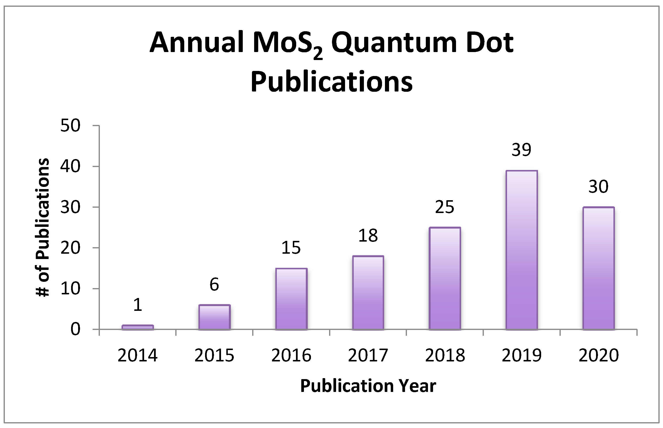
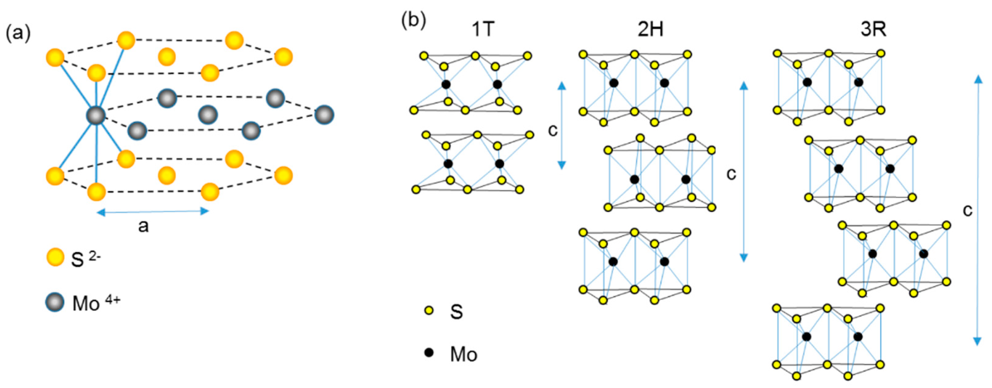
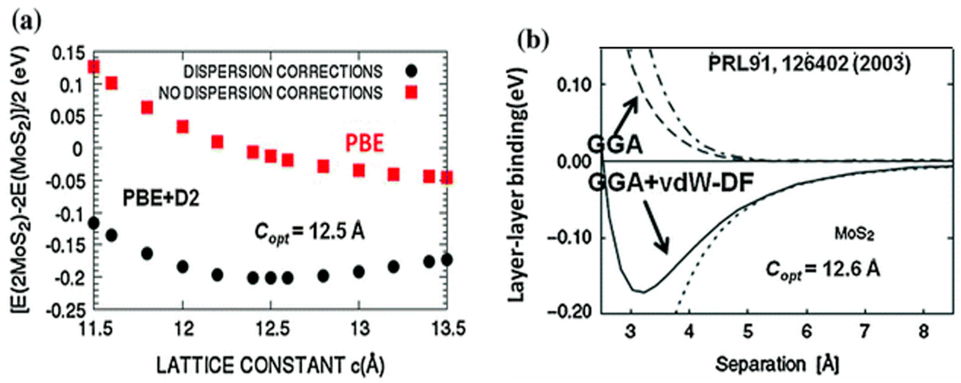
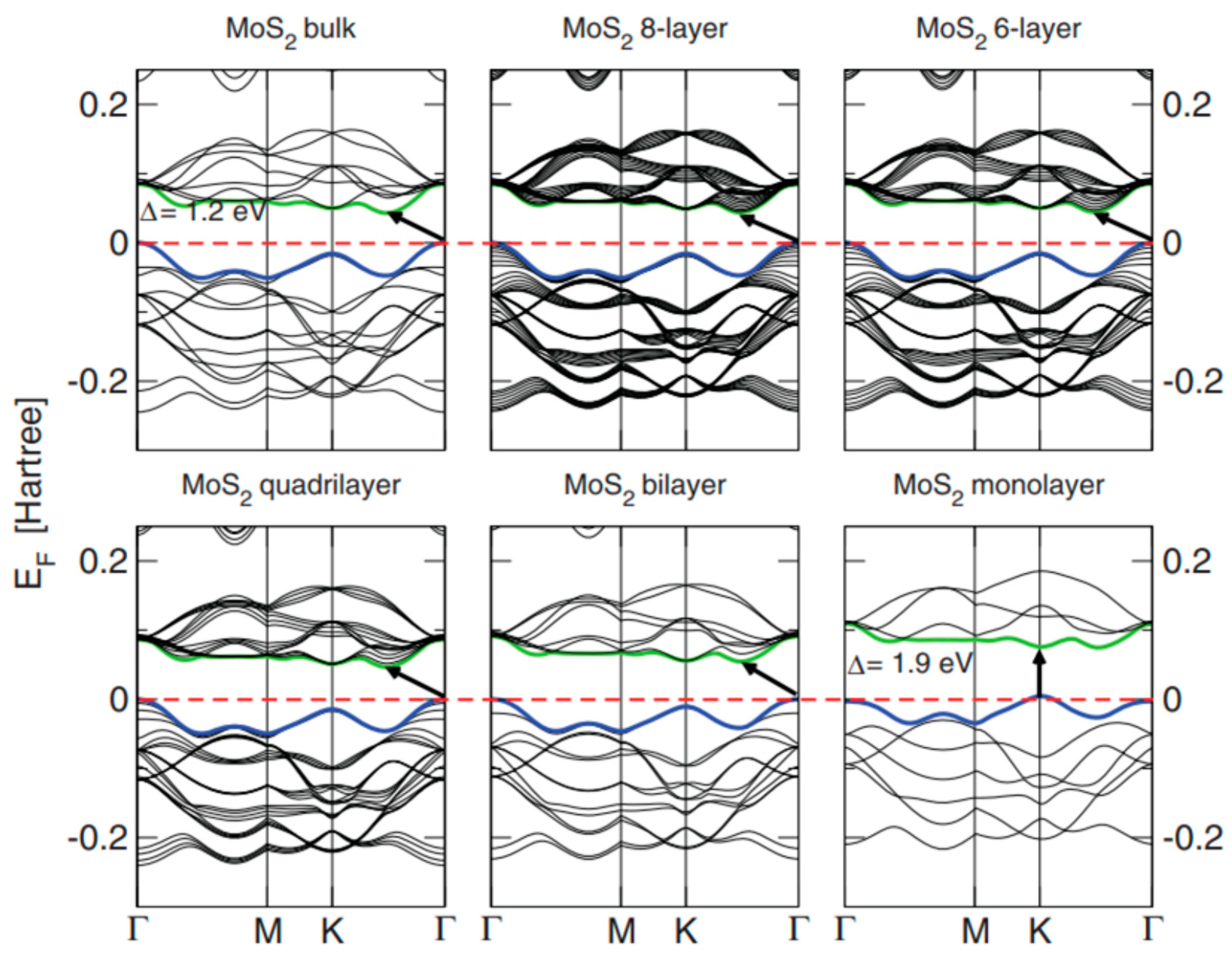
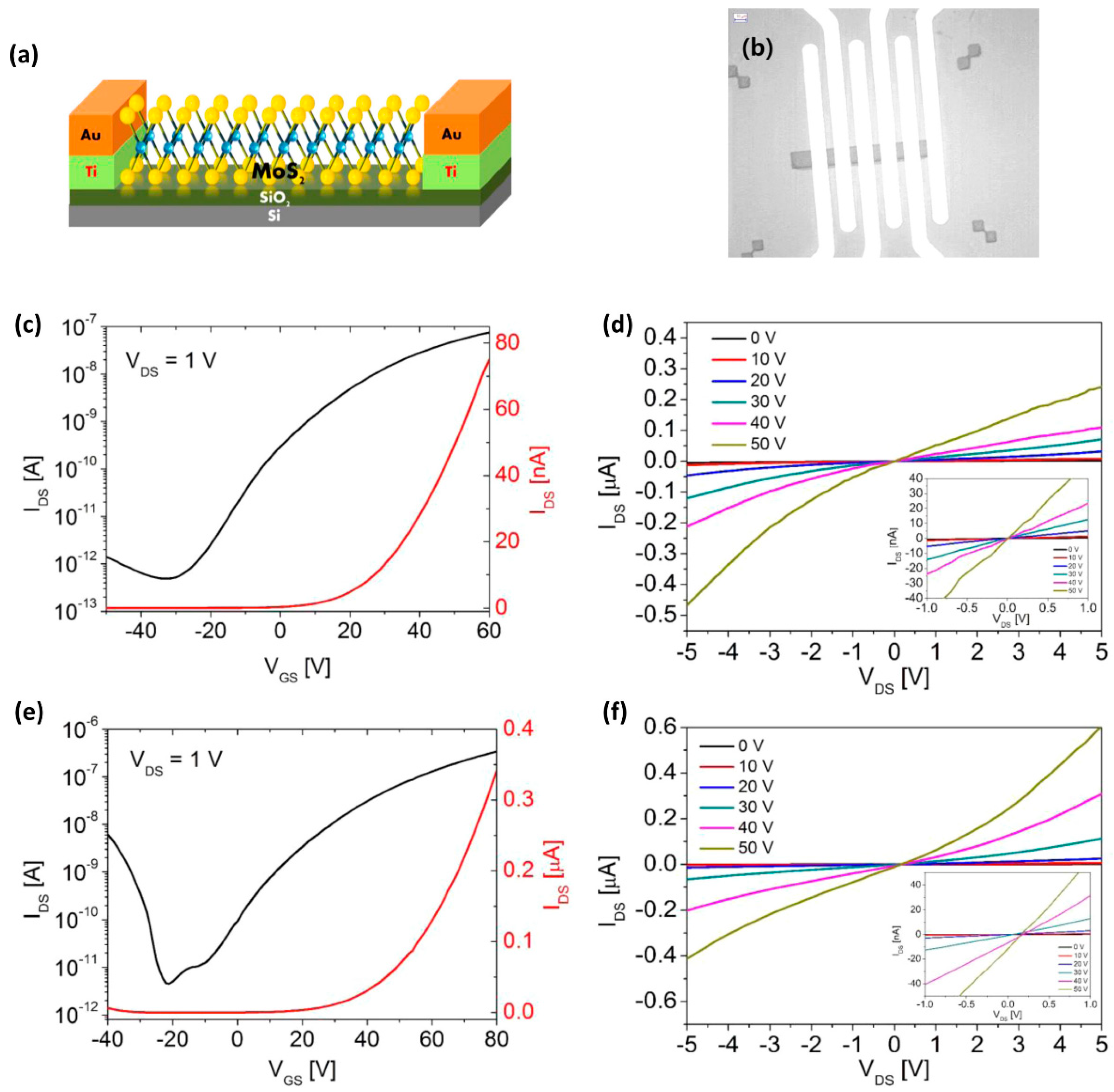
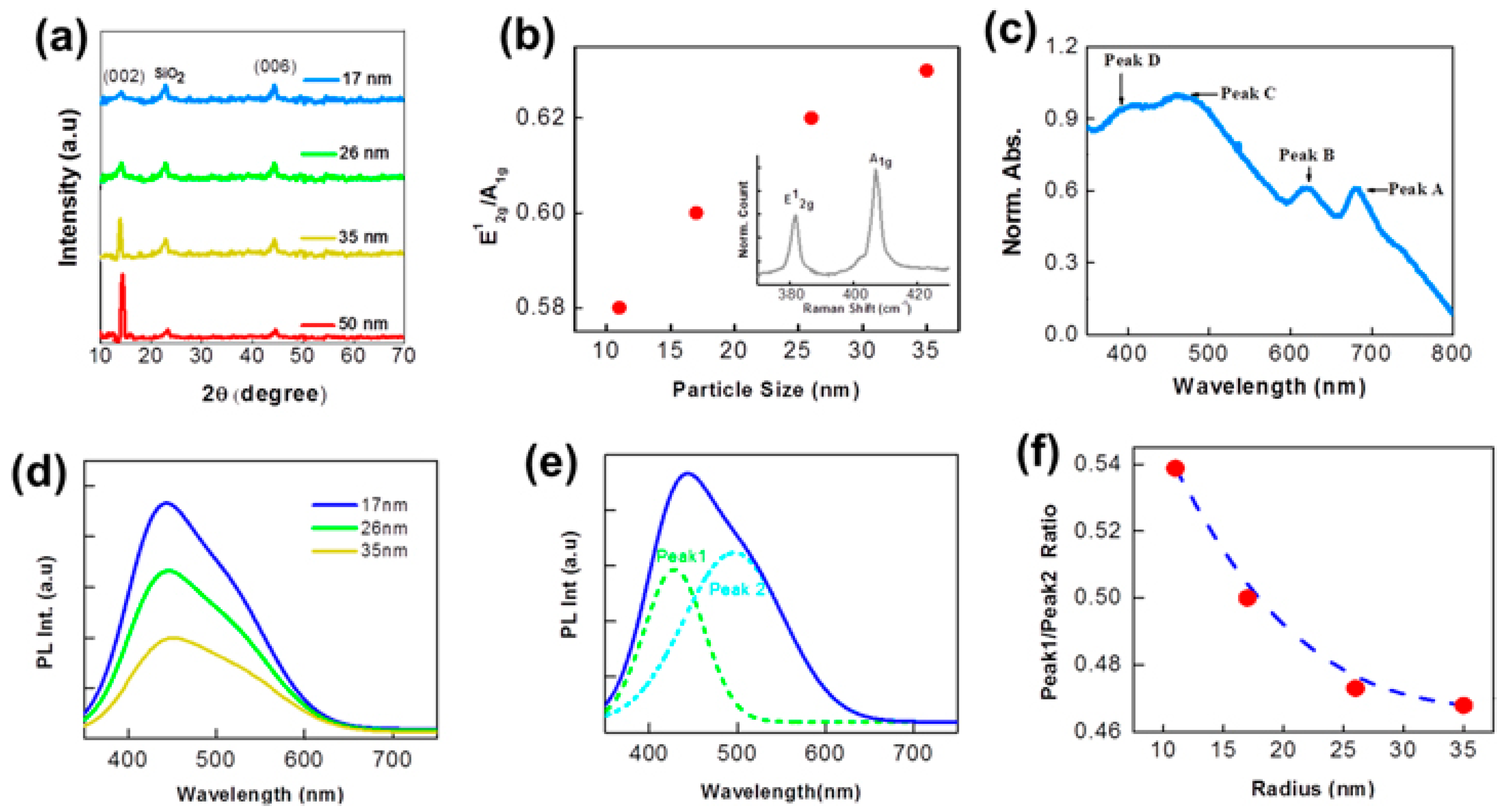
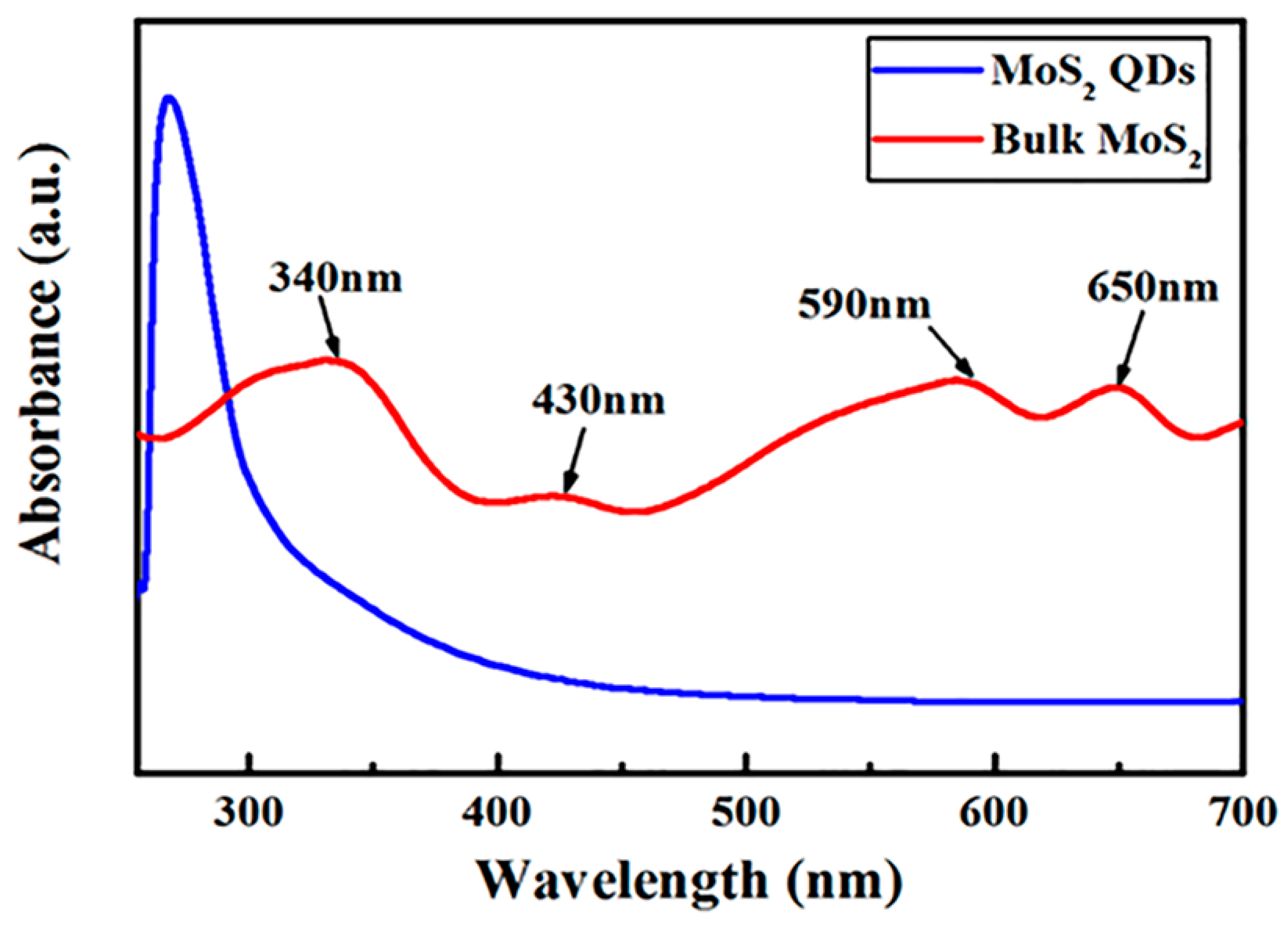
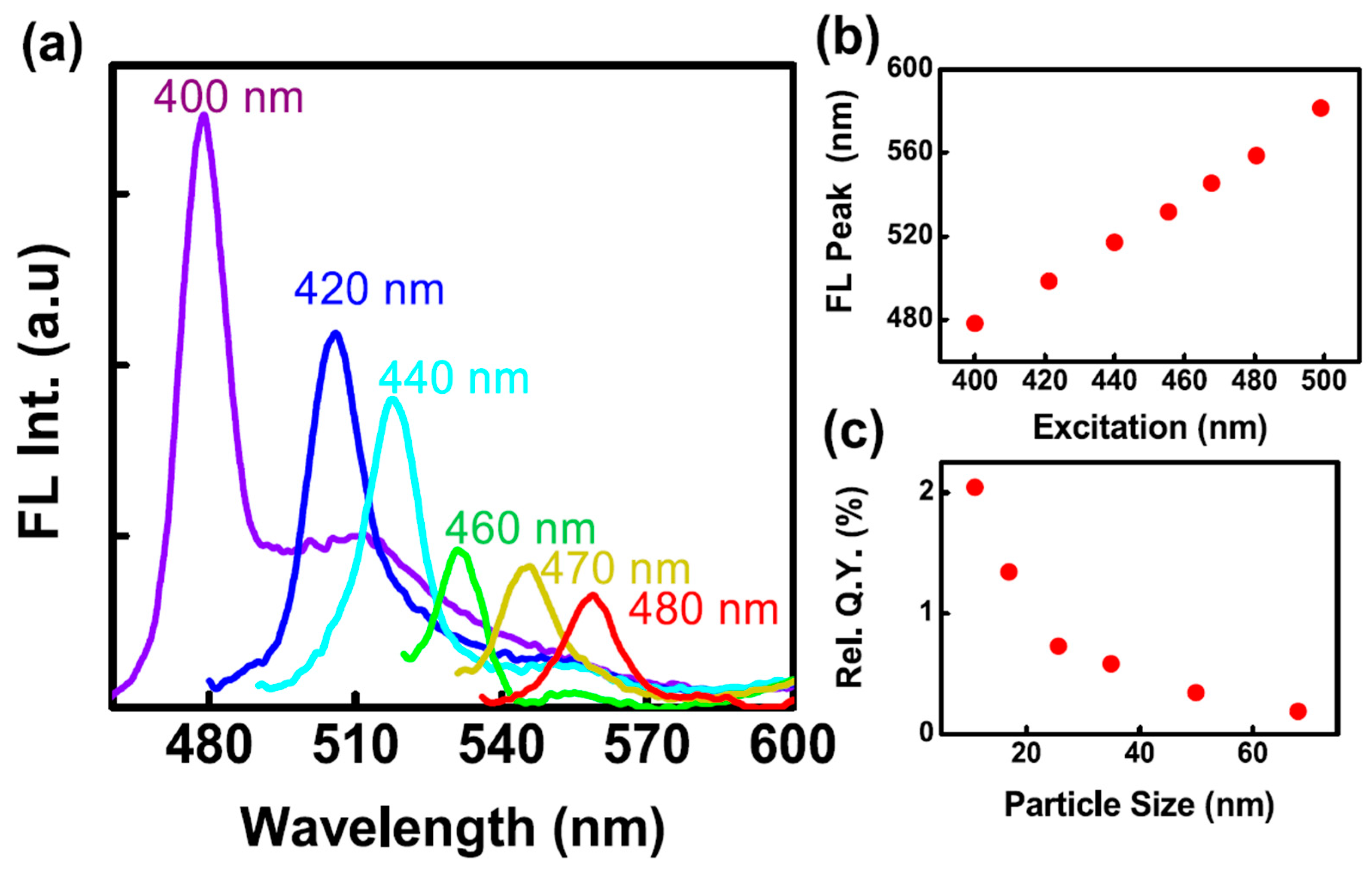
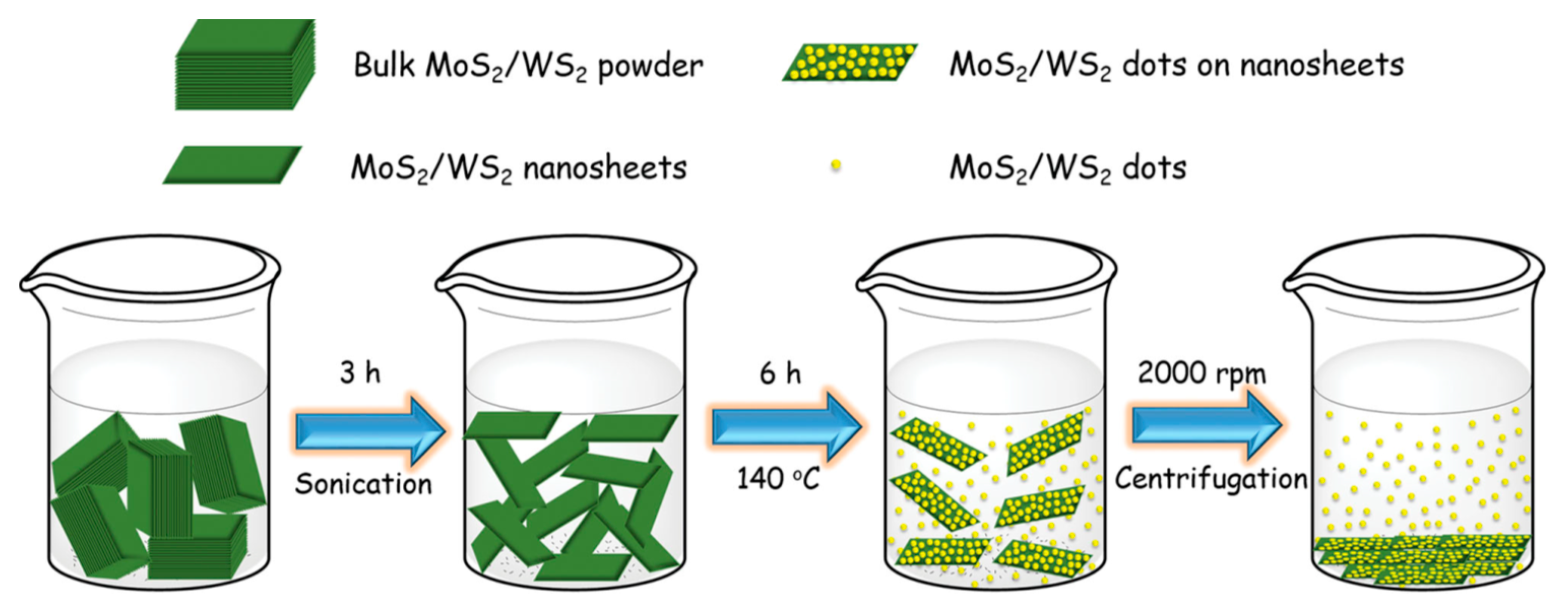
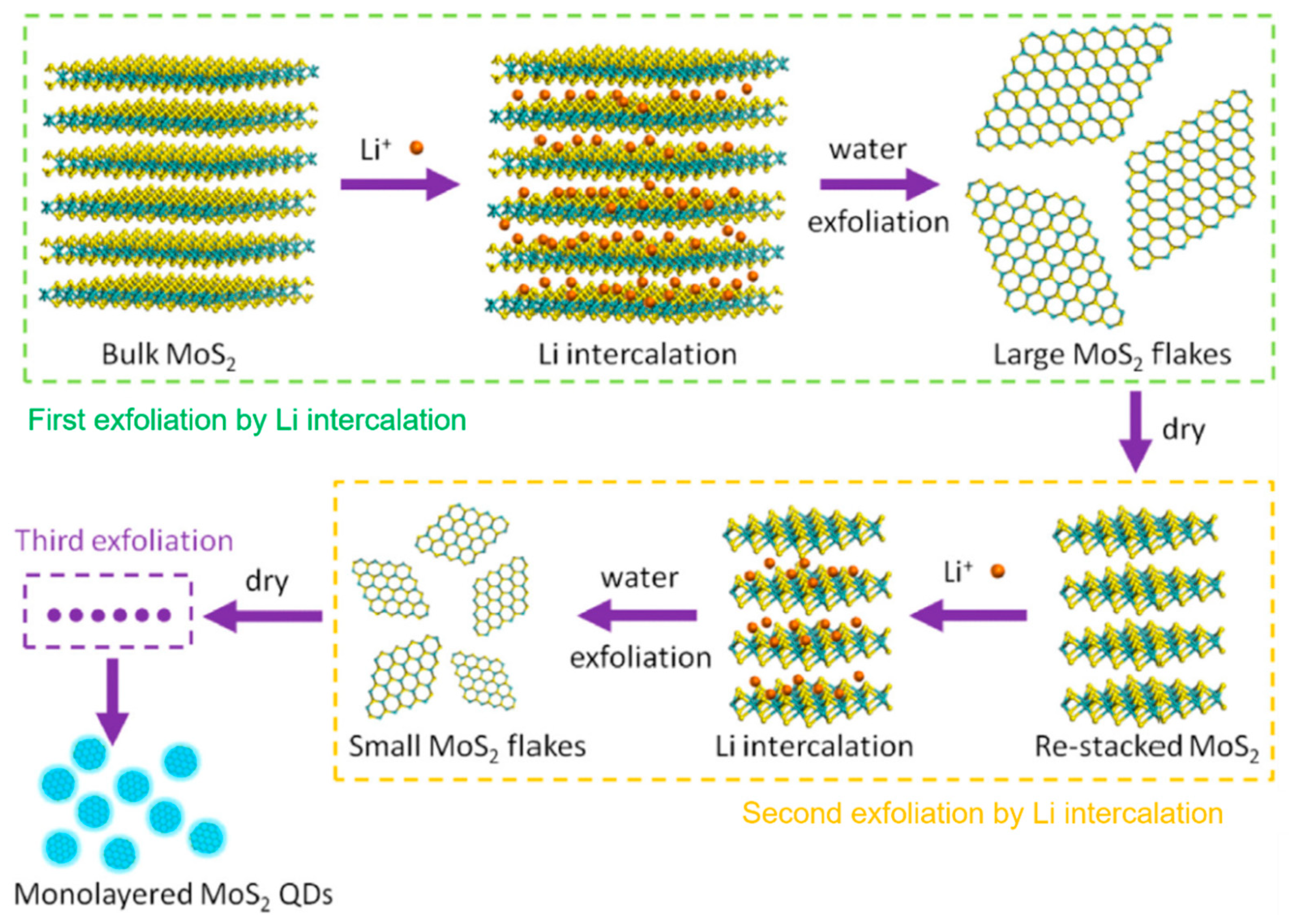
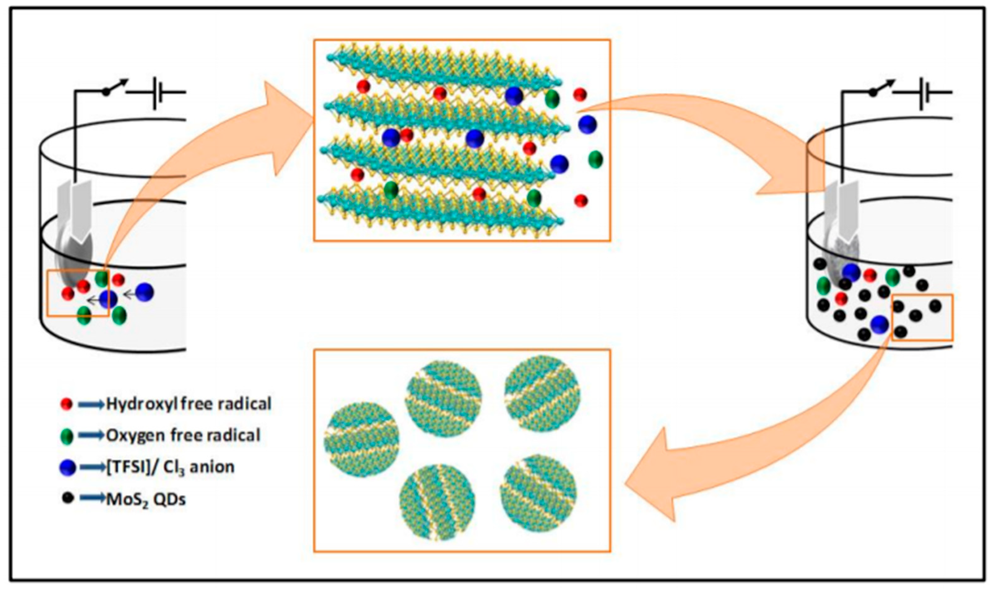
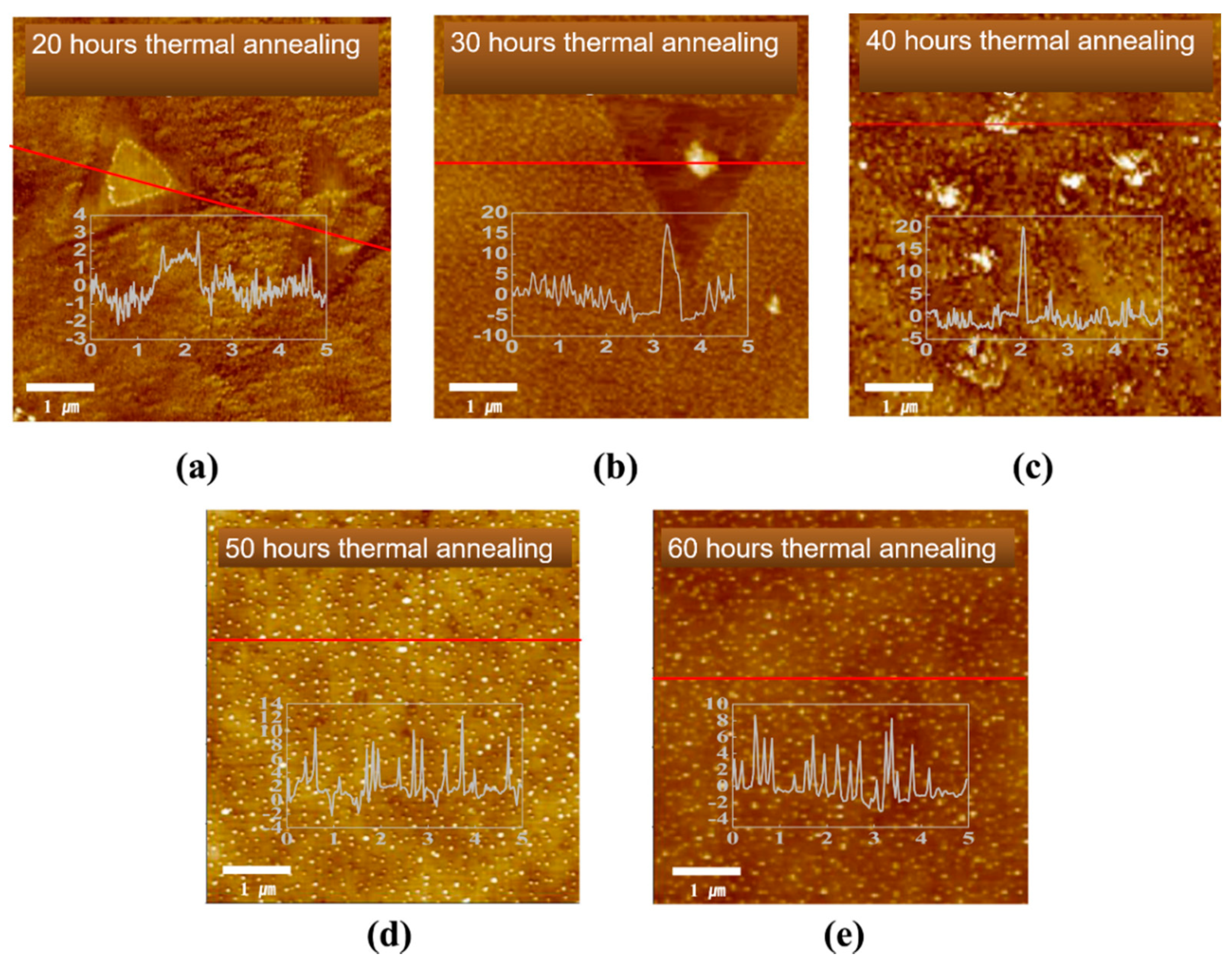
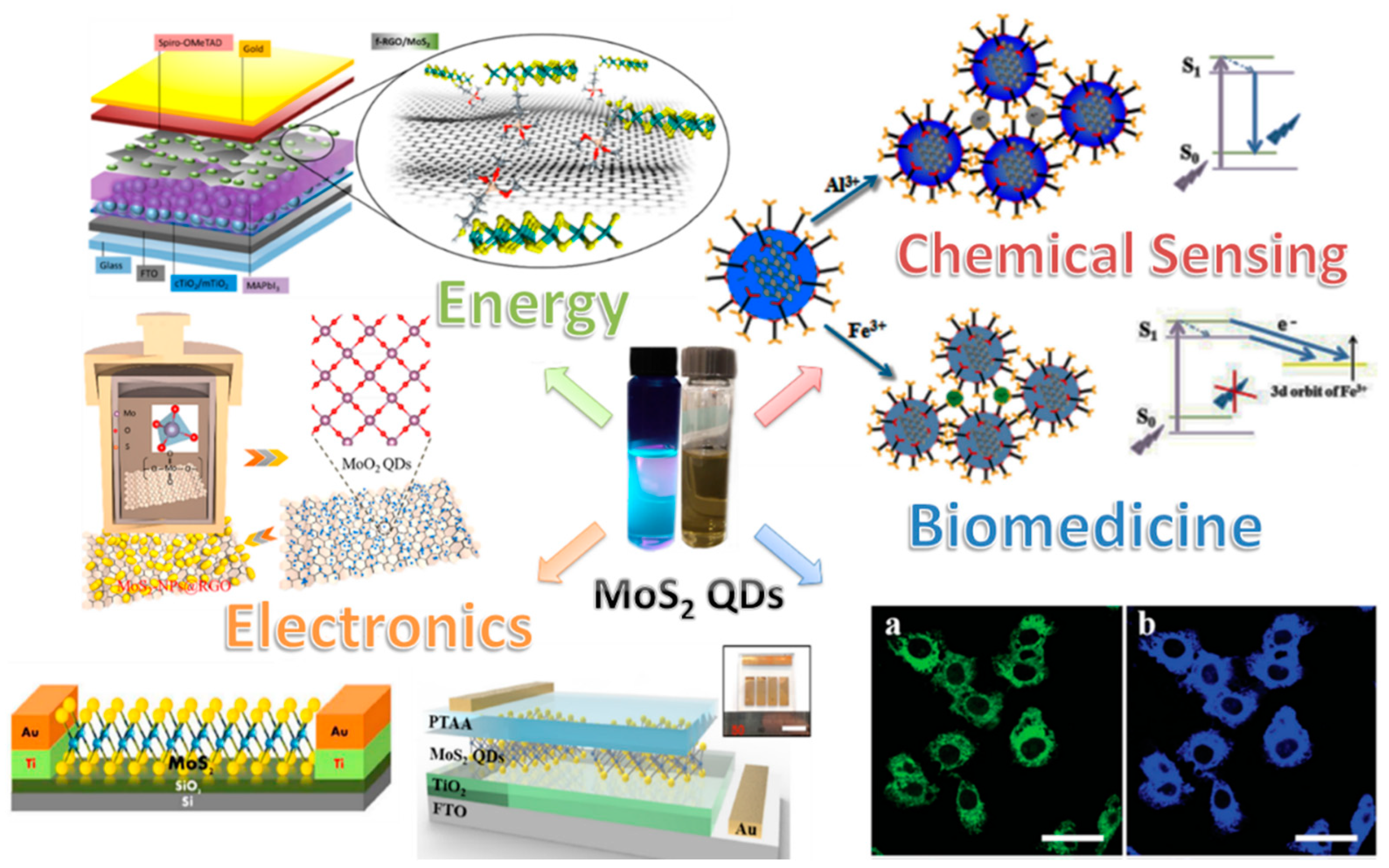
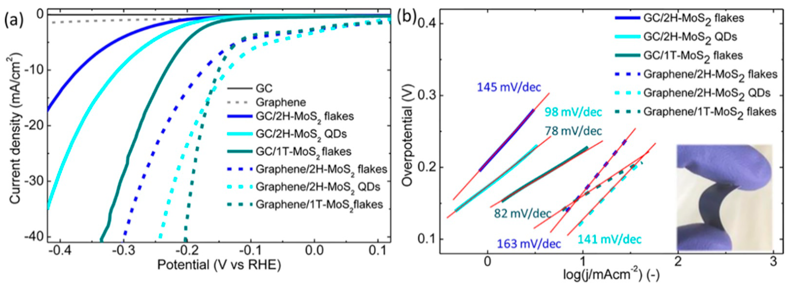
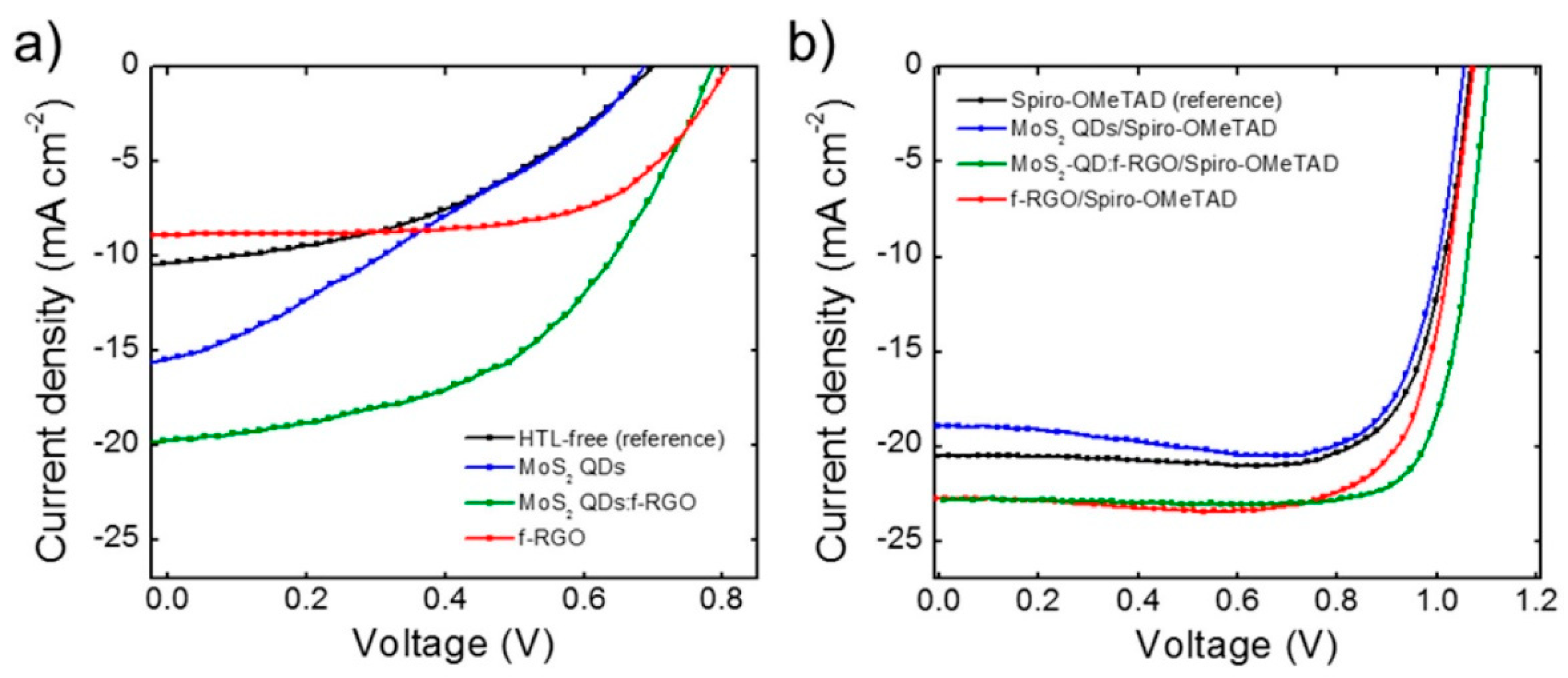
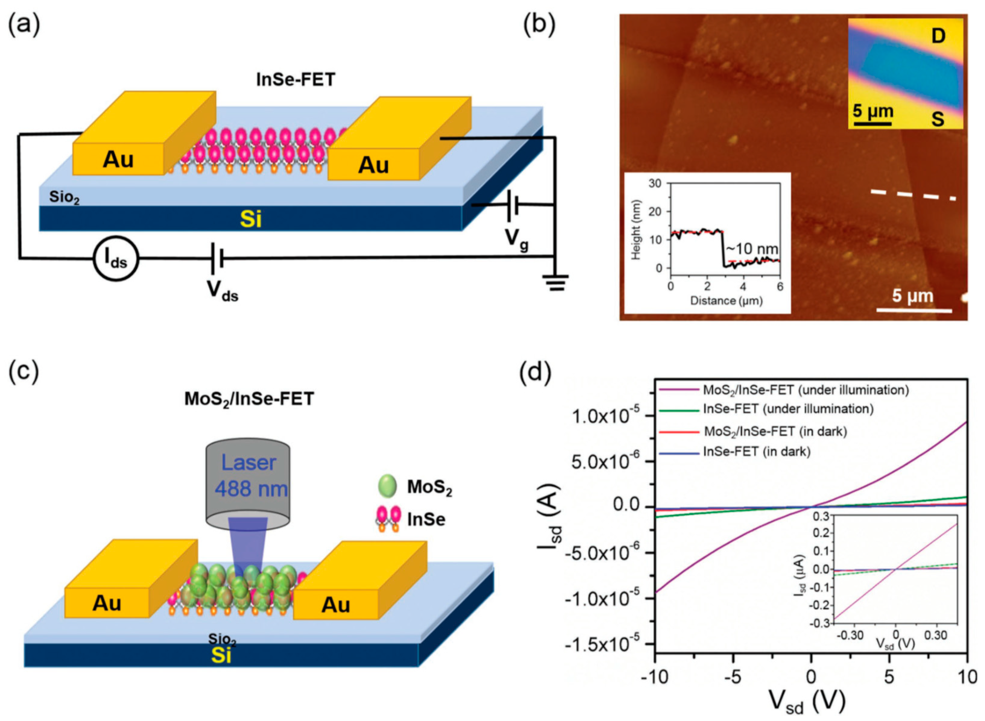
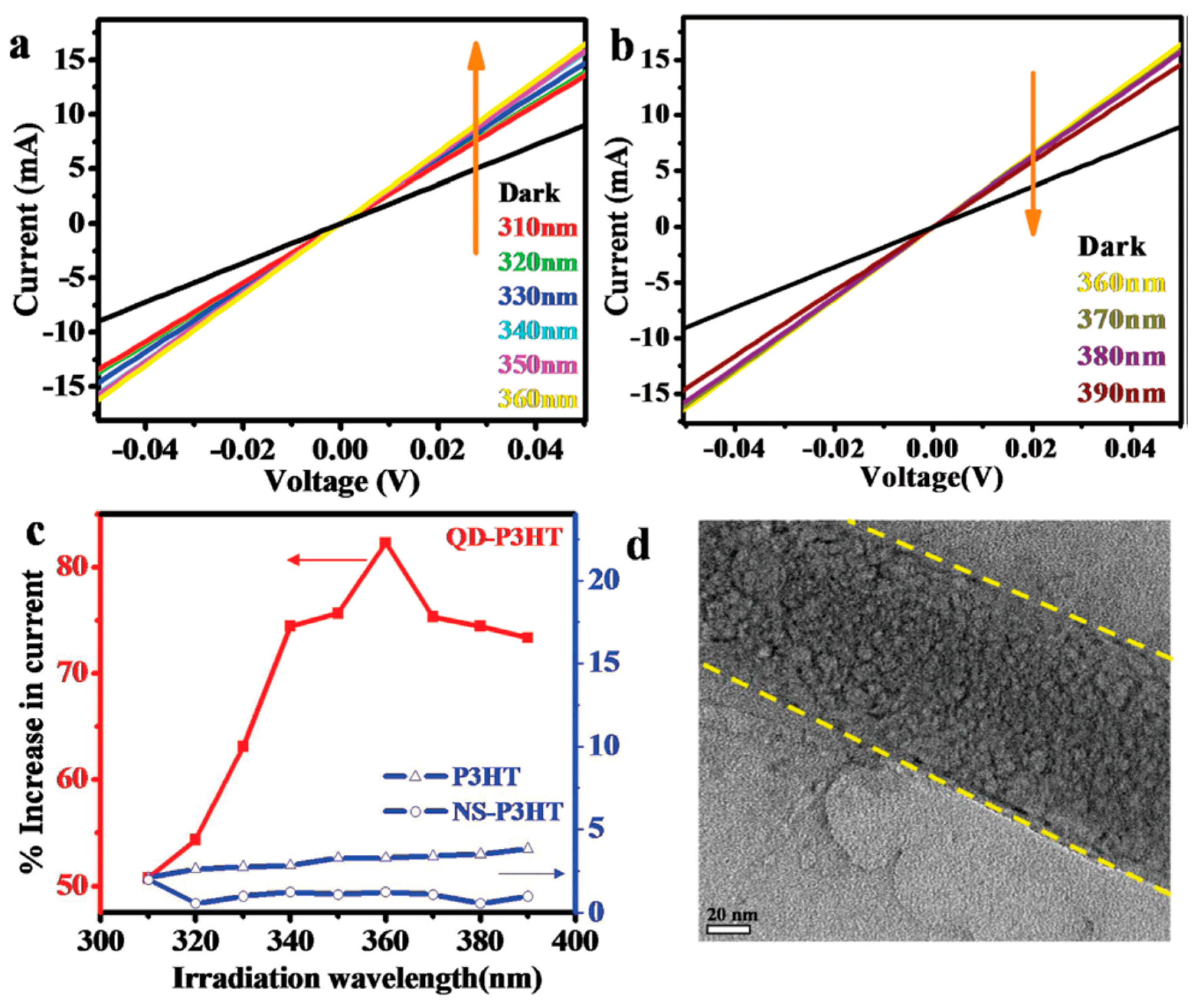
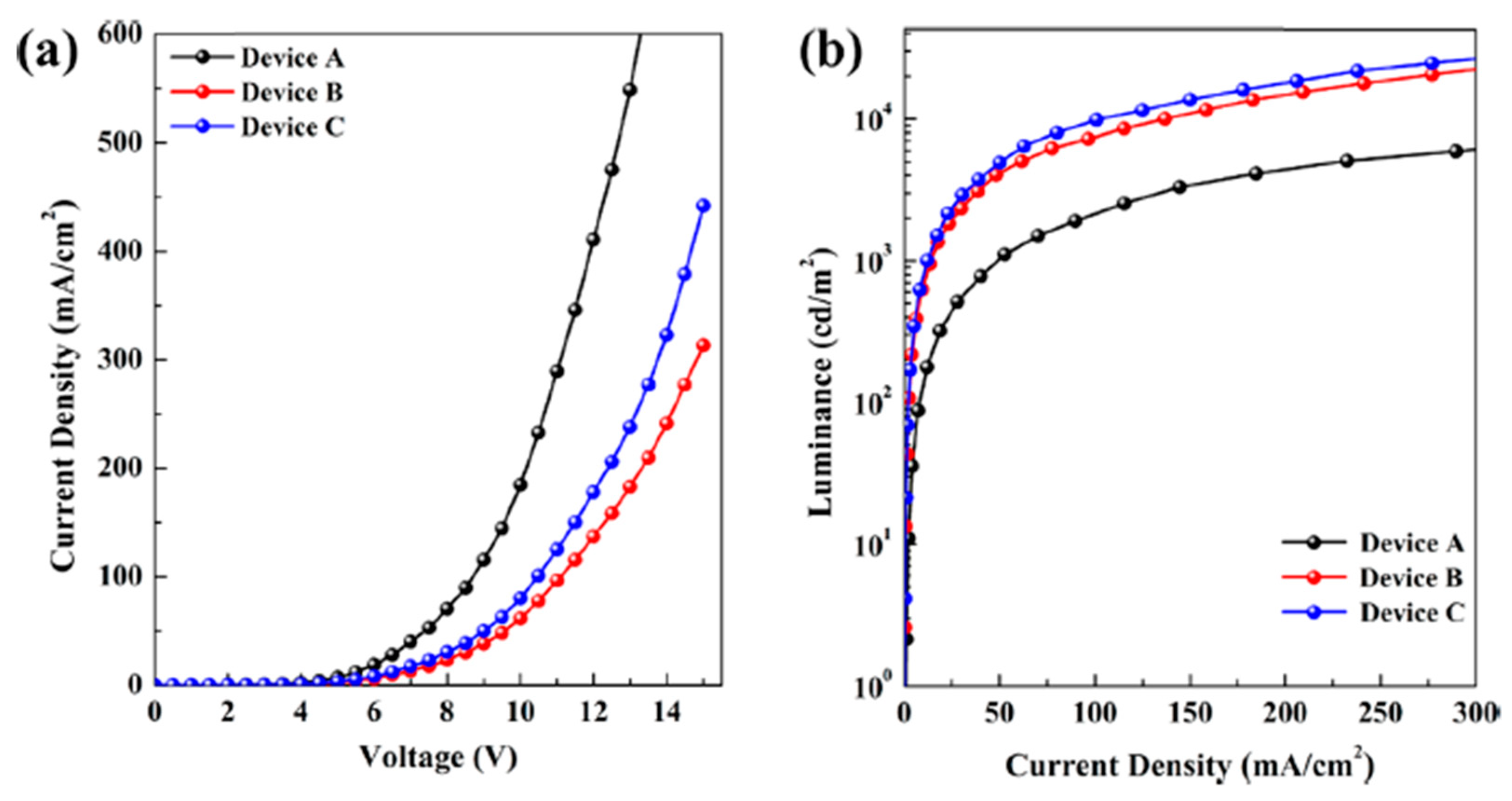
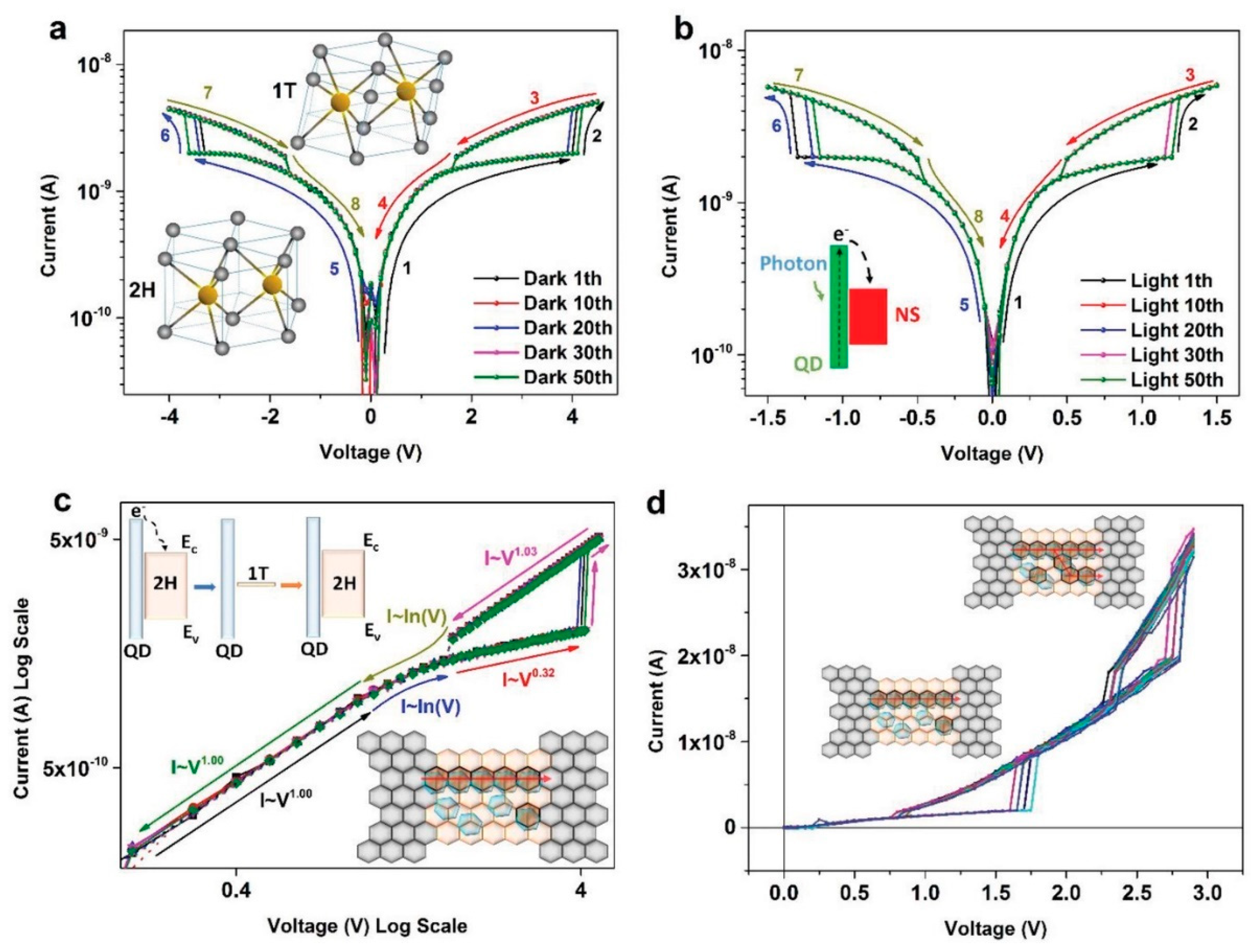
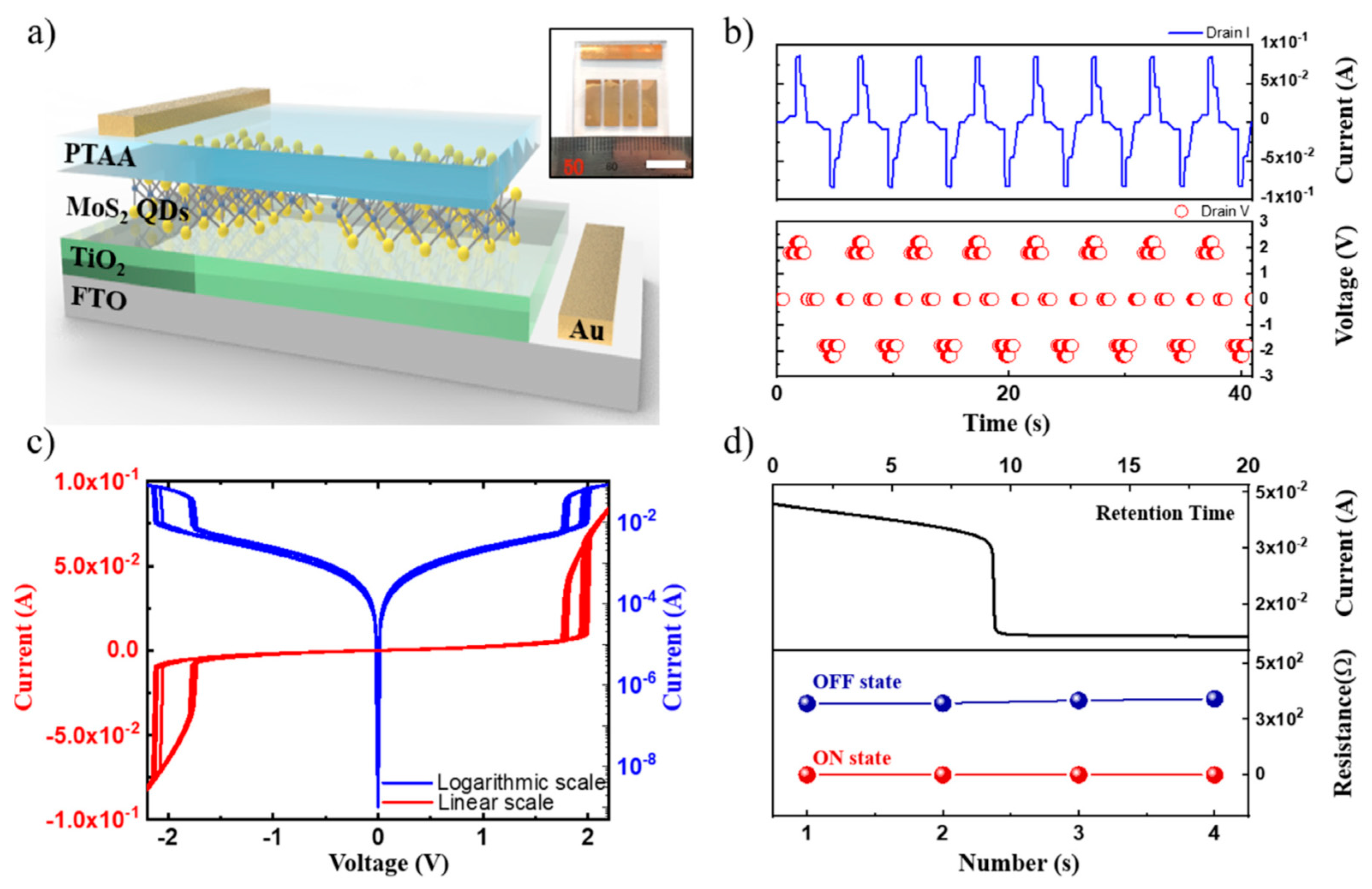
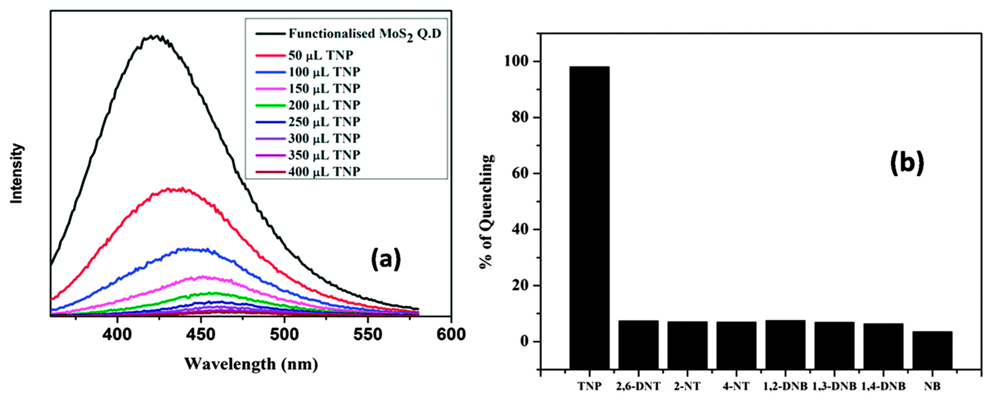
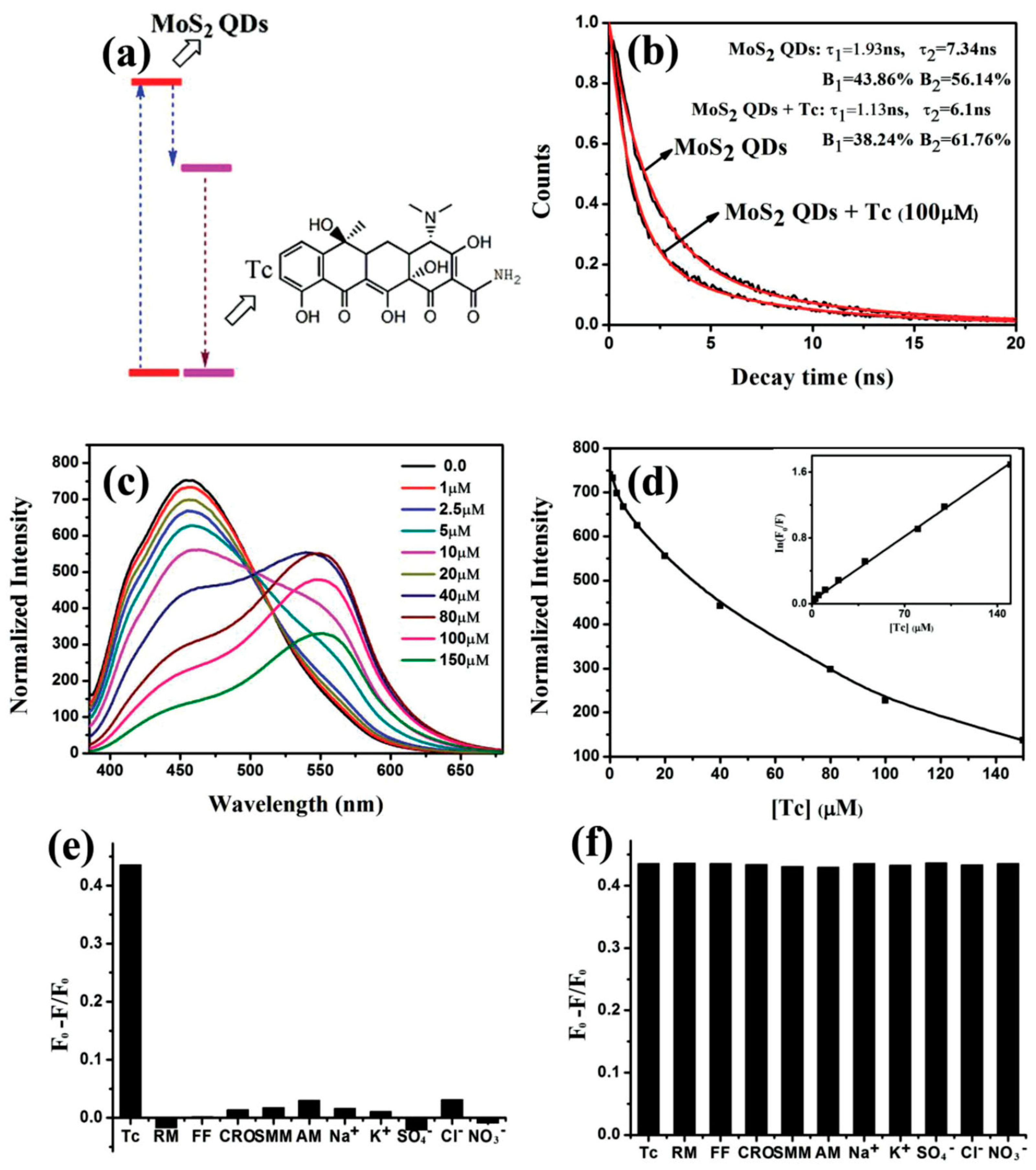
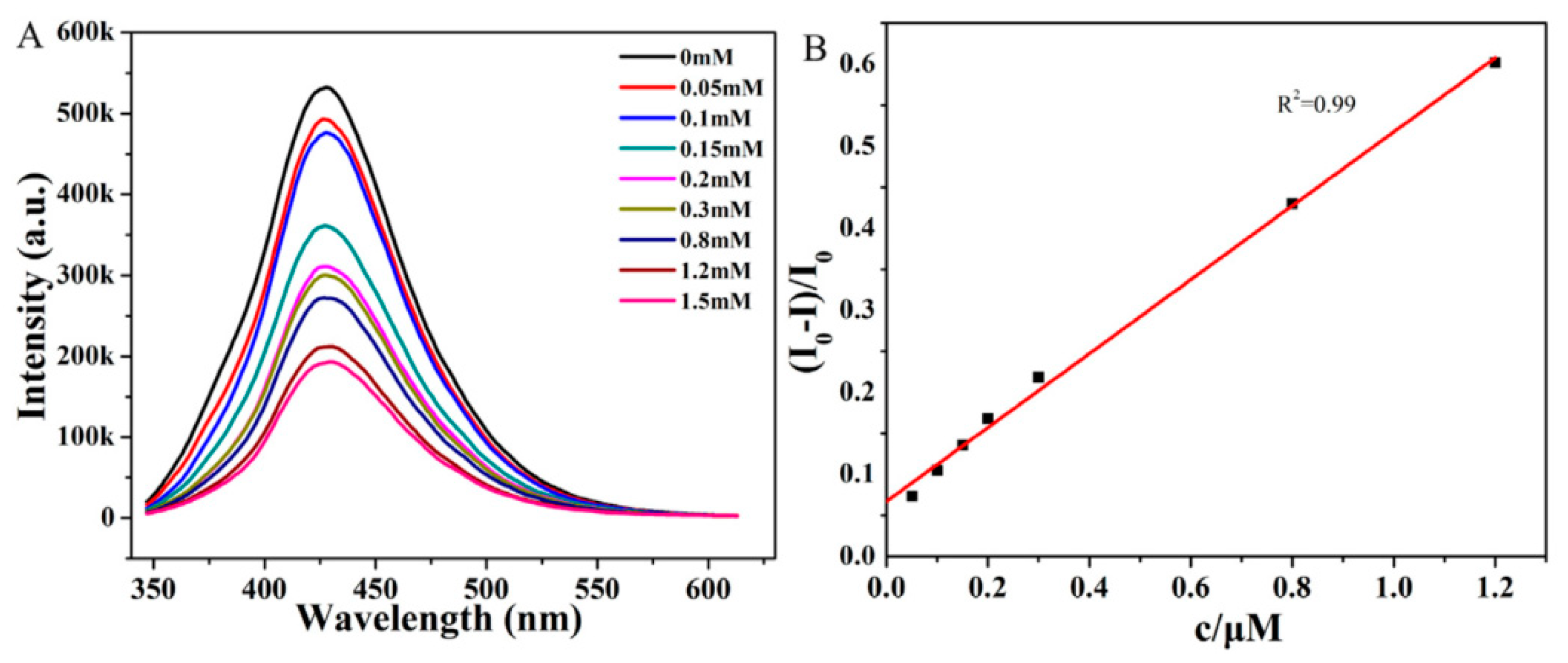
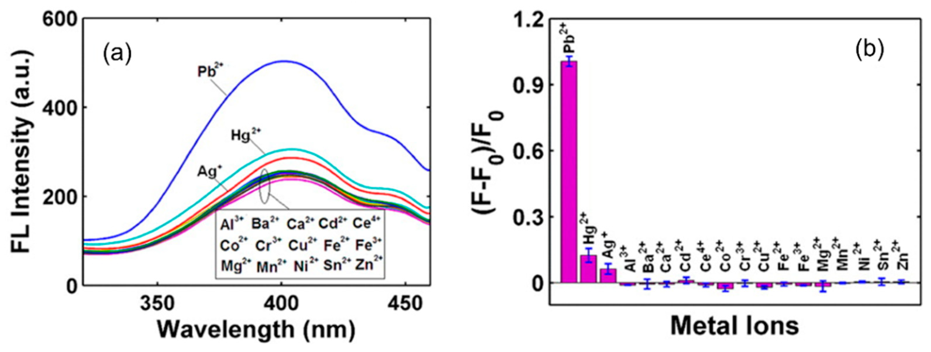
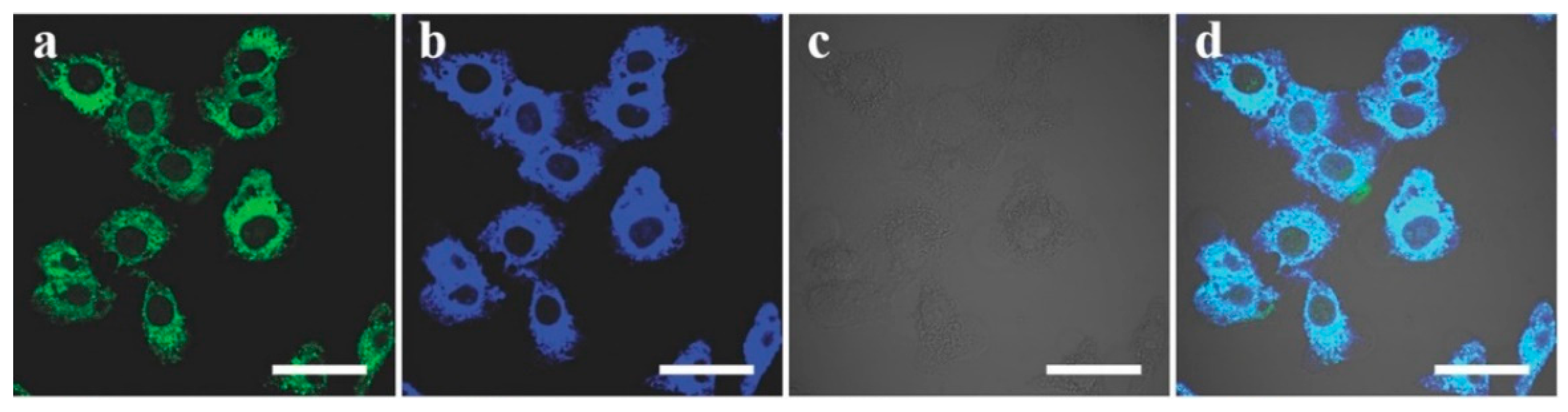
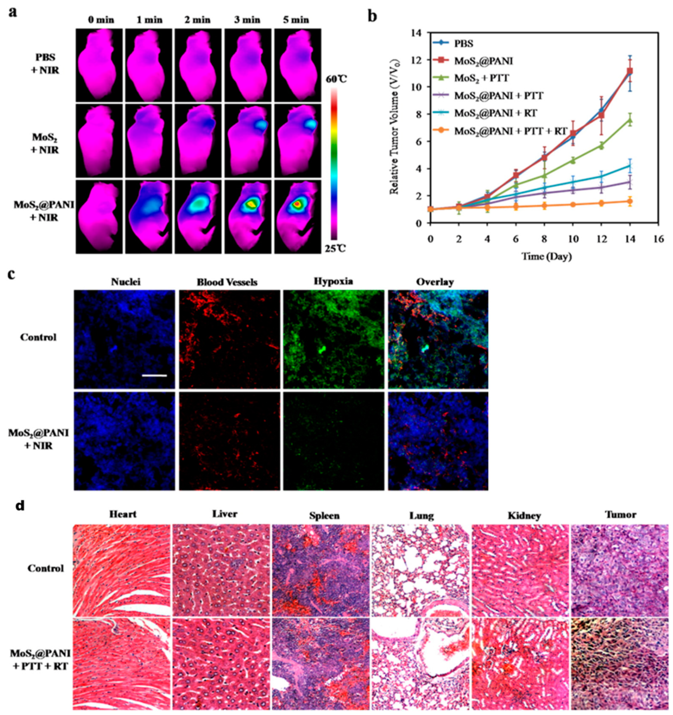
Table 1.
Methods of sonication-assisted synthesis of MoS2 QDs and experimental parameters.
| Solvents | Notes | Emission (Excitation) | Size | Reference |
|---|---|---|---|---|
| Ethylene Glycol | Natural molybdenite suspended in the solvent and sonicated in a pressurized ultrasound reactor for 20 min, and then refluxed at 193 °C for 24 h. Dispersion filtered using Pragopor membrane. | 440 nm (350 nm) | 4–70 nm, 1 nm thick | [65] |
| Sulfuric Acid | MoS2 powder suspended in sulfuric acid and sonicated at 65 °C for 20 h. The solution was centrifuged for 30 min, dialyzed, and filtered. | 425 nm (300 nm) | 3.5 nm, 1–1.5 thick | [60] |
| DMF, NMP, DMEU, DI water, ethanol, acetone | Six solvents were tested. MoS2 powder suspended in a solvent and sonicated for 3 h. The top two-thirds were decanted and refluxed for 6 h below the solvent’s boiling point. The solution was allowed to sit for several hours, then centrifuged for 5 min. The supernatant was evaporated under vacuum, and the QDs were resuspended in DI water. | DMF: 465 nm (390 nm) NMP: 455 nm (380 nm) | DMF: 3.3 nm (avg.), 1.2 nm thick NMP: 3.4 nm DMEU: 3–4 nm | [43] |
| NMP | MoS2 powder dispersed in the solvent and sonicated it continuously in an ice bath for 3.5 h before tip sonicating it for another 3.5 h. The dispersion was left undisturbed overnight and then centrifuged for 90 min. | 575 nm (400 nm) | 0.5–4.0 nm (2.5 nm avg.) | [66] |
| Liquid Nitrogen + IPA | Heated MoS2 powder in a quartz boat to 340 °C under ambient air and maintained it for 3 min. Immediately after, it was quenched in a Dewar flask of liquid nitrogen. Once the liquid nitrogen was fully evaporated, quenched MoS2 was dispersed in IPA and sonicated for 30 min using a cycle of 7 s “on” and 3 s “off”. The solution was centrifuged for 30 min. | 440 nm (360 nm) | 1.41 nm (avg.), 1.5 nm thick | [67] |
Table 2.
Hydrothermal synthesis of MoS2 quantum dots with various precursors.
| Precursors | Emission (Excitation) | Size | Reference |
|---|---|---|---|
| Sodium molybdate + Glutathione | 425 nm (340 nm) | 2.7 ± 0.3 nm (avg.) spherical | [74] |
| Sodium molybdate + L-cysteine | 402 nm (308 nm) | 3.5 nm, 1–1.5 thick | [75] |
| Sodium molybdate + Dibenzyl-disulfides | 280 nm (205 nm) | DMF: 3.3 nm (avg.), 1.2 nm thick NMP: 3.4 nm DMEU: 3–4 nm | [75] |
| Sodium molybdate + Thiourea | 406 nm (250 nm) | 0.5–4.0 nm (2.5 nm avg.) | [77] |
| [(NH4)6Mo7O24 • 4H2O] + Sodium Sulfide | 1.41 nm (avg.), 1.5 nm thick | [78] | |
| Molybdenyl acetylacetonate + Thioglycolic Acid + Sodium Sulfide | [79] | ||
| (NH4)6Mo7O24 + Thiourea + N-acetyl- l-cysteine | 480 nm (380 nm) | 2.1 nm (avg.) < 0.9 nm thick | [69] |
| (NH4)2MoS + N2H4 | 400 nm (330 nm) | 2.8 nm (avg.) 1.4–2.5 nm thick | [80] |
| (NH4)2MoS + Oleylamine | 575 nm (500 nm) | 4.5 ± 0.5 nm (avg.) 3 nm thick | [81] |
Table 3.
Use of MoS2 QDs in HER.
| Material | Overpotential (mV) | Tafel Slope (mV/dec) | Reference |
|---|---|---|---|
| MoS2 QDs in Aerogel | 53 | 41 | [89] |
| MoS2 QDs between MoS2 Nanosheets | 190 | 74 | [66] |
| MoS2 QDs on Glassy Carbon | 210 | 60 | [44] |
| MoS2 QDs | 140 | 66 | [48] |
| MoS2 QDs on Graphene Flakes | 136 | 141 | [90] |
| MoS2 QDs | 160 | 59 | [76] |
| Fe-doped MoS2 QDs | 121 | [91] | |
| Li-doped MoS2 QDs | 109 | [91] | |
| Mg-doped MoS2 QDs | 91 | [91] | |
| MoS2 QDs on Au | 130 | 94 | [39] |
| MoS2 QDs | 120 | 115 | [44] |
Table 4.
Uses of MoS2 QDs in solar cell technology and reported power conversion efficiencies.
| Design | PCE (%) | Reference |
|---|---|---|
| MoS2 on F-doped SnO2 as a Counter Electrode | 3.69 | [93] |
| MoS2 QDs/InSe–FET | 3.03 | [94] |
| MoS2 QDs with UV–ozone on MoS2 Nanosheets | 8.66 | [95] |
| MoS2 QDs on Graphene Flakes | 20.12 | [82] |
Table 5.
Chemical Sensing Capabilities of MoS2 QDs.
| Chemical | Selectivity | Concentration | Reference |
|---|---|---|---|
| 2,4,6–trinitrophenol | F0/F = 1.42 | 10.0 μm | [75] |
| 2,4,6–trinitrophenol | F/F0 = 0.95 | 1.0 mM | [78] |
| Pb | (F- F0)/F0 > 0.9 | 5.0 μm | [77] |
| S | (F- F0)/F0 > 0.3 | 10.0 μm | [77] |
| Tetracycline hydrochloride | (F- F0)/F0 > 0.4 | 0.05 mM | [79] |
| Glucose | (F- F0)/F0 = 0.17 | 0.5 mM | [74] |
| Al | (F- F0)/F0 > 2.7 | 1.0 mM | [83] |
| Fe | (F- F0)/F0 > 0.5 | 1.0 mM | [83] |
Publisher’s Note: MDPI stays neutral with regard to jurisdictional claims in published maps and institutional affiliations. |
© 2021 by the authors. Licensee MDPI, Basel, Switzerland. This article is an open access article distributed under the terms and conditions of the Creative Commons Attribution (CC BY) license (https://creativecommons.org/licenses/by/4.0/).
Share and Cite
MDPI and ACS Style
Kabel, J.; Sharma, S.; Acharya, A.; Zhang, D.; Yap, Y.K. Molybdenum Disulfide Quantum Dots: Properties, Synthesis, and Applications. C 2021, 7, 45. https://0-doi-org.brum.beds.ac.uk/10.3390/c7020045
AMA Style
Kabel J, Sharma S, Acharya A, Zhang D, Yap YK. Molybdenum Disulfide Quantum Dots: Properties, Synthesis, and Applications. C. 2021; 7(2):45. https://0-doi-org.brum.beds.ac.uk/10.3390/c7020045
Chicago/Turabian StyleKabel, Jeff, Sambhawana Sharma, Amit Acharya, Dongyan Zhang, and Yoke Khin Yap. 2021. "Molybdenum Disulfide Quantum Dots: Properties, Synthesis, and Applications" C 7, no. 2: 45. https://0-doi-org.brum.beds.ac.uk/10.3390/c7020045
Note that from the first issue of 2016, this journal uses article numbers instead of page numbers. See further details here.