Article

The Growth Behavior of Amorphous Hydrogenated Carbon a-C:H Layers on Industrial Polycarbonates—A Weak Interlayer and a Distinct Dehydrogenation Zone

1
Department of Physics, University Koblenz-Landau, 56070 Koblenz, Germany
2
Key Laboratory of Marine New Materials and Related Technology, Zhejiang Key Laboratory of Marine Materials and Protection Technology, Ningbo Institute of Materials Technology and Engineering, Chinese Academy of Sciences, Ningbo 315201, China
3
Materials Science, Energy and Nano-Engineering Department, Mohammed VI Polytechnic University, Ben Guerir 43150, Morocco
*
Authors to whom correspondence should be addressed.
Submission received: 29 June 2021 / Revised: 22 July 2021 / Accepted: 26 July 2021 / Published: 29 July 2021

Abstract

:
Polycarbonate (PC) is a material that is used in many areas: automotive, aerospace engineering and data storage industries. Its hardness is of particular importance, but some applications are affected by its low wettability or scratch susceptibility. This can be changed either by blending with other polymers, or by surface modifications, such as the application of an amorphous hydrogenated carbon layer (a-C:H). In this study, individual a-C:H layers of different thicknesses (10–2000 nm) were deposited on PC by RF PECVD. Both the layer morphology with AFM and SEM and the bonding states of the carbon on the surface with synchrotron-assisted XPS and NEXAFS were studied. The aim was to investigate the coatability of PC and the stability of the a-C:H. Special attention was paid to the interlayer region from 0 to 100 nm, since this is responsible for the layer to base material bonding, and to the zone of dehydrogenation (from about 1000 nm), since this changes the surface composition considerably. For PC, the interlayer was relatively small with a thickness of only 20 nm. Additionally, a correlation was found between the evolving grain structure and the development of the C‒H peak according to NEXAFS C K-edge measurements.

1. Introduction

Polycarbonate (PC) is a transparent polymer and is used in many technical applications due to its advantageous mechanical properties and its processability. For example, it is utilized not only in aerospace and automotive engineering, but also in the construction industry and optical lenses [1,2,3]. However, PC itself has disadvantages, such as high hydrophobicity and notch sensitivity. These properties can be modified—for example, by blending with other thermoplastic polymers [2]. Another way to influence these properties is to deposit a (thin) layer of amorphous carbon (a-C) or amorphous hydrogenated carbon (a-C:H) on its surface [4,5,6,7,8]. These carbon layers consist of a network of π–sp2, σ–sp2 and sp3 hybridized carbon atoms in which the hydrogen is embedded [6,9,10].
The wettability of these layers is influenced by the morphology [11,12] and the chemical bonds on the surface [13,14], as well as by the carbon bonds present on the surface (sp2 or sp3 hybridized) [15,16,17,18]. Coatings with a-C:H are suitable for altering the wettability of the surface sustainably [5,8,19,20]. The ratio of the carbon hybridization states can be influenced by the plasma parameters during the coating process, the gas used, the amount of hydrogen [6,9,17,21,22] and the coating thickness itself [19,20,23]. This carbon state ratio also affects the scratch resistance of the coating obtained. If the sp2/sp3 ratio is very low, a very hard, diamond-like coating is obtained (high hardness, chemical inertness and high electrical resistance) [21]. If the proportion of sp3 bonds on the surface is reduced in favor of the sp2 bonds, the layer has graphite-like properties, such as improved electrical conductivity on the surface of the coated material [21].
Various techniques can be used to deposit such a-C:H layers: e.g., ion beam deposition, magnetron sputtering and radio frequency plasma enhanced chemical vapor deposition (RF-PECVD) [6,21,23,24]. The latter was used in this study to deposit coatings on PC, as its low process temperatures make it ideal for coating non-conductive polymers [21,25].
However, before such a layer can be used to specifically influence the properties of such a material, the basic coatability must first be investigated. The important question is whether an interlayer forms and how pronounced it is. The interlayer is a mixed phase of the base material and the a-C:H layer deposited by the plasma. During the plasma process, the species which are generated interact with the substrate via impinging and surface reorganization [26]; additionally, material from the substrate may be eroded and incorporated into the forming layer. These processes lead to better crosslinking of the two systems, and the more pronounced the interlayer is, the better the adhesion of the a-C:H layer [24]. Polyoxymethylene (POM), for example, does not form a measurable interlayer; the layer can simply be detached [27]. High-density polyethylene (HDPE), on the other hand, has a very pronounced interlayer that is 40 nm thick and has very good connectivity to the polymer [8,28]. As soon as the plasma has hardly any influence on the base material, the interlayer formation is completed and regular layer growth begins. Furthermore, it must be determined whether the so-called dehydrogenation of the layers takes place as soon as a certain layer thickness is exceeded [5,8,27,28,29]. Here, hydrogen is released from the a-C:H layer, whereby the proportion of sp2-bonded carbon increased at the expense of the sp3 bonds, which ultimately influenced the layers’ properties. The layer stability itself and the detection of non-stable layer thicknesses must also be checked in advance.
In the current study, these investigations were carried out for the transparent polymer PC. By RF-PECVD technique and acetylene plasma, a-C:H layers of various thicknesses (0–2000 nm) were deposited and examined. Special attention was paid to the a-C:H layer from 10 to 50 nm. Fine subdivisions were used here, since the interlayer manifests itself in this range. The layer stability was investigated ex situ by scanning electron microscopy (SEM). A more microscopic view of the surface morphology was possible with atomic force microscopy (AFM). Finally, the carbon bond states at the film’s surface were analyzed by X-ray photoelectron spectroscopy (XPS) and near-edge X-ray absorption fine structure (NEXAFS).

2. Materials and Methods

2.1. Sample Preparation

PC material was supplied as 2 mm thick sheets by Goodfellow (Bad Nauheim, Germany). It was of industrial quality. Samples with Ø 10 mm were stamped out and subsequently cleaned with isopropanol in an ultrasonic bath. For the coating, they were mounted on a vacuum-compatible aluminum holder and placed in a vacuum chamber at a distance of 275 mm in front of the plasma source. The high frequency plasma source used was a Copra DN 400 (CCR GmbH, Troisdorf, Germany) operating at 13.65 MHz [24]. The coating of the sample surface was processed in two separate plasma processes: first, the samples were cleaned and activated for 10 min in oxygen plasma. Second, an acetylene plasma was used for the a-C:H coating. The process duration depended on the desired coating thickness [5,8,27]. The processes can be read about in detail elsewhere [23]. During the plasma processes, the sample temperature never exceeded 40 °C [25]. Different layer thicknesses from 0 (O2-treated PC sample) to 2000 nm were realized this way. The thickness intervals were variable and depended on the thickness range investigated: 0–100 nm in 10 nm steps in the interlayer region, 100–1000 nm in 100 nm steps and 1000–2000 nm in 250 nm steps. The coating rates were, apart from small variations in initial growth, constant over time and were about 10 nm/min [23]. In order to check the coating thicknesses subsequently, silicon wafers partially covered with aluminum foil were coated together with the PC samples. The thickness of each deposited layer was determined using a profilometer (Dektak 3, Veeco Instruments Inc., Plainview, NY, USA) [23].

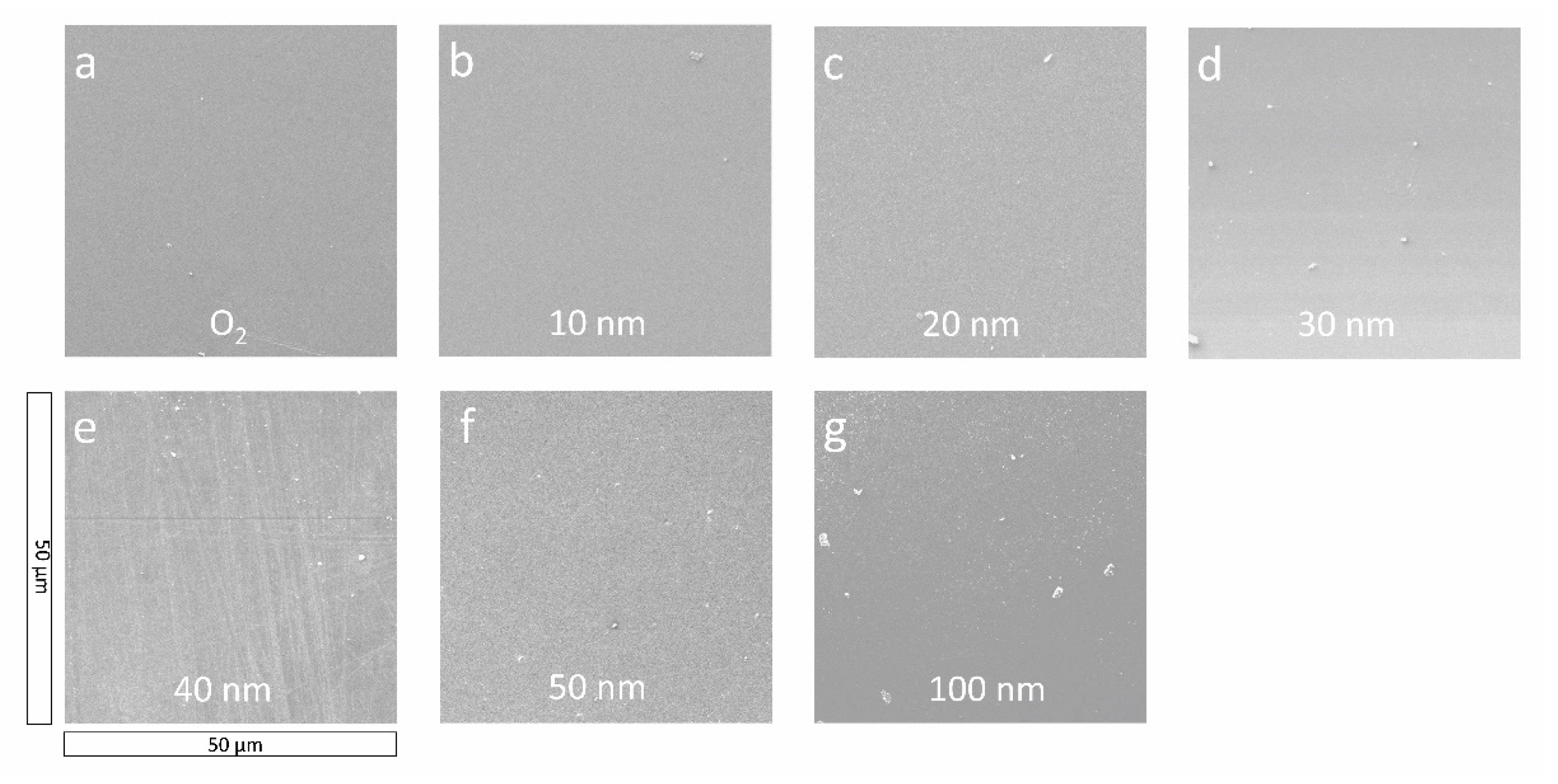
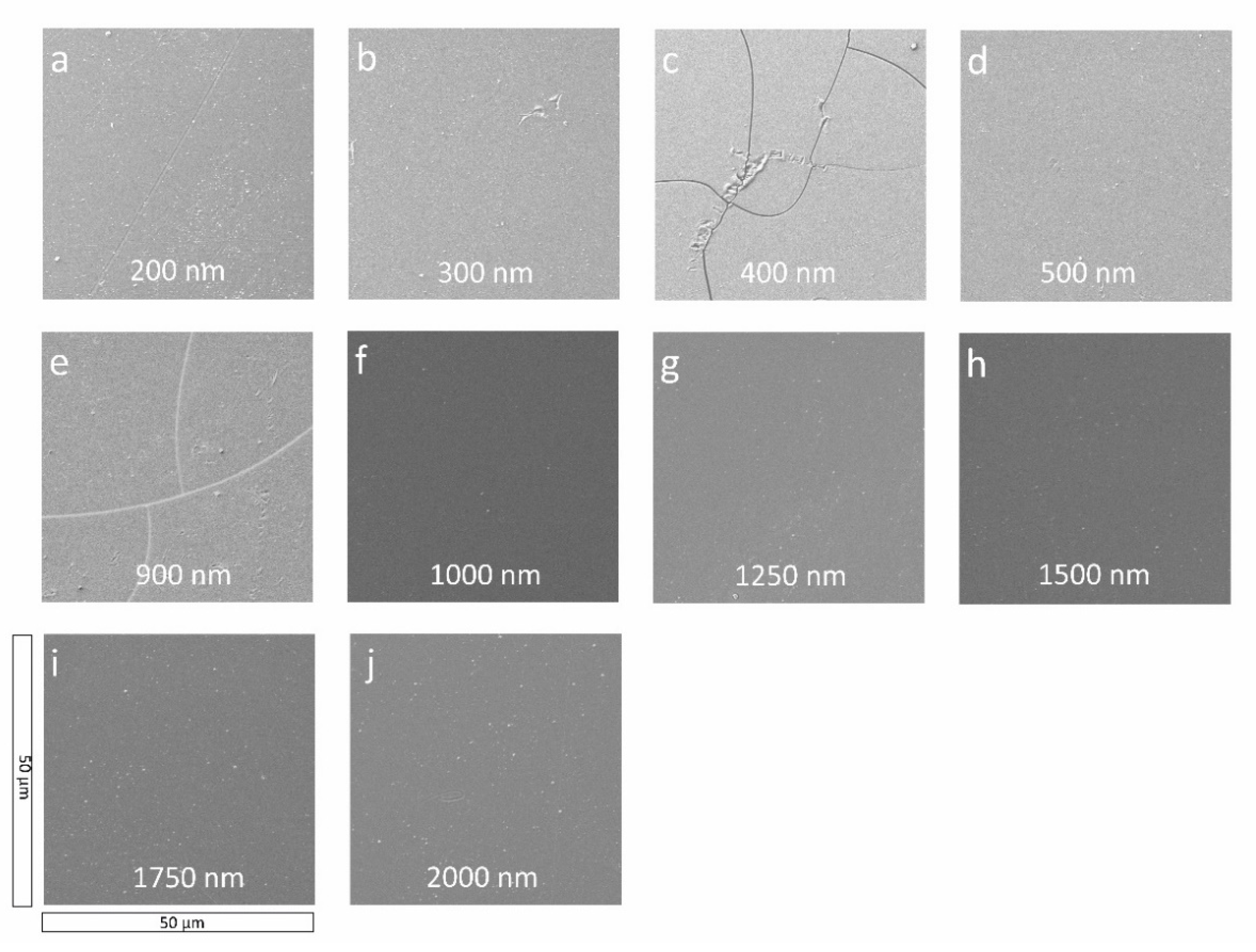
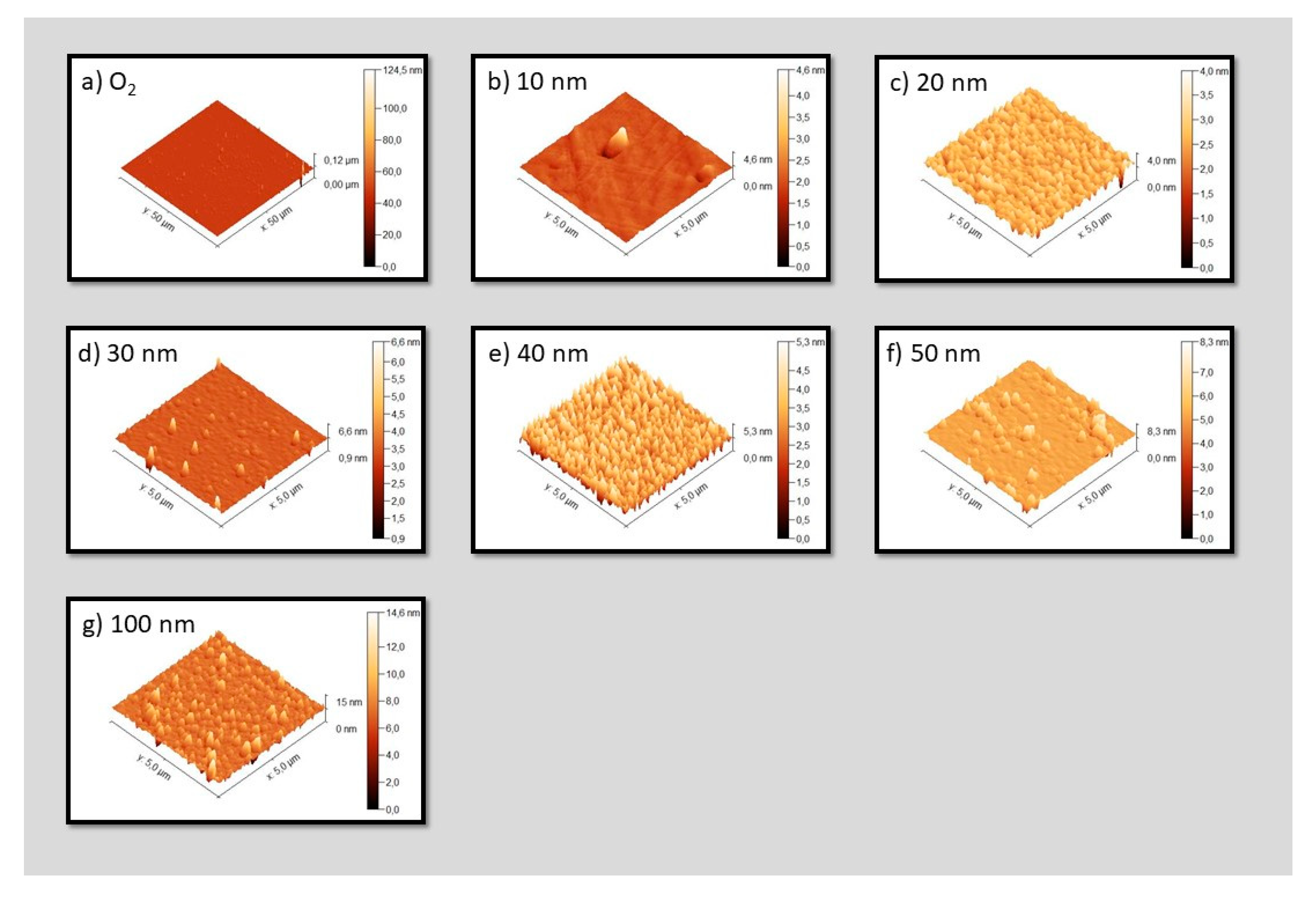
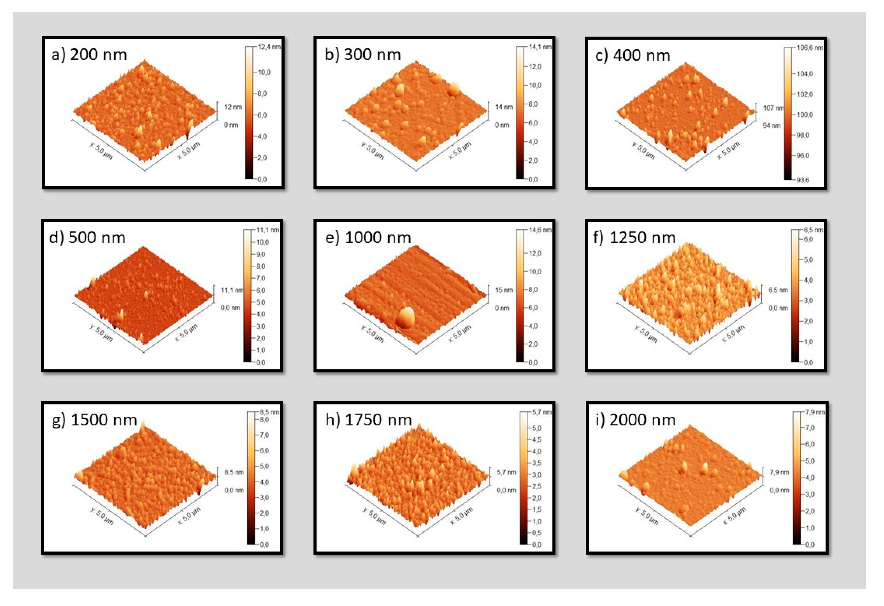
2.2. Sample Surface Morphology

The analysis of each sample’s surface structure was carried out in two steps. A scanning electron microscope (SEM515, Phillips, 7 kV, WD 20 mm, FEI Company, Amsterdam, The Netherlands) was first used to perform more macroscopic examinations. The SEM images provided information on the stability of the film and whether it was intact. However, for this technique, a 7–10 nm thick gold layer must first be applied to the sample’s surface to increase the conductivity. This is to avoid charging effects or even beam damage by the electron beam. A more detailed analysis of the surface was obtained with an atomic force microscope (AFM, Asylum Research, Oxford Instruments MFP-3D-BIO). The AFM was operated in contact mode with AC240-TS tips from Oxford Instruments in ambient conditions. For both microscopy techniques the measurements were repeated in at least three locations to ensure homogeneity of the surface. The AFM data obtained were then analyzed using Gwyddion (open source, version 2.58). First, a plane correction was performed. Subsequently, a mean and a median filter were used, followed by a conservative noise reduction. These steps are the same as those which were used by Catena et al. [5,8,27]. Finally, the zero level was shifted to the minimum high value of the sample surface for a unified representation. Roughness, through Rq and Ra, was evaluated, and images were exported accordingly. Due to the small measuring range, however, the layer integrity cannot be determined, which is why the SEM and AFM techniques complement each other.

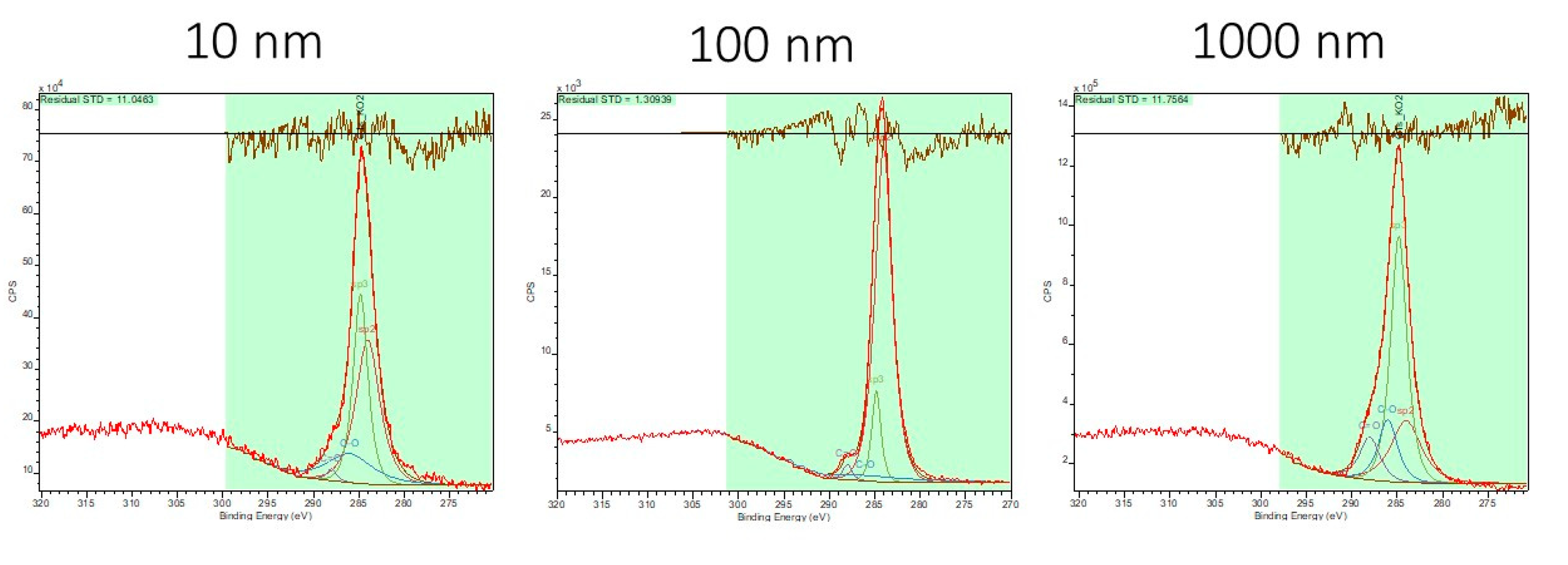
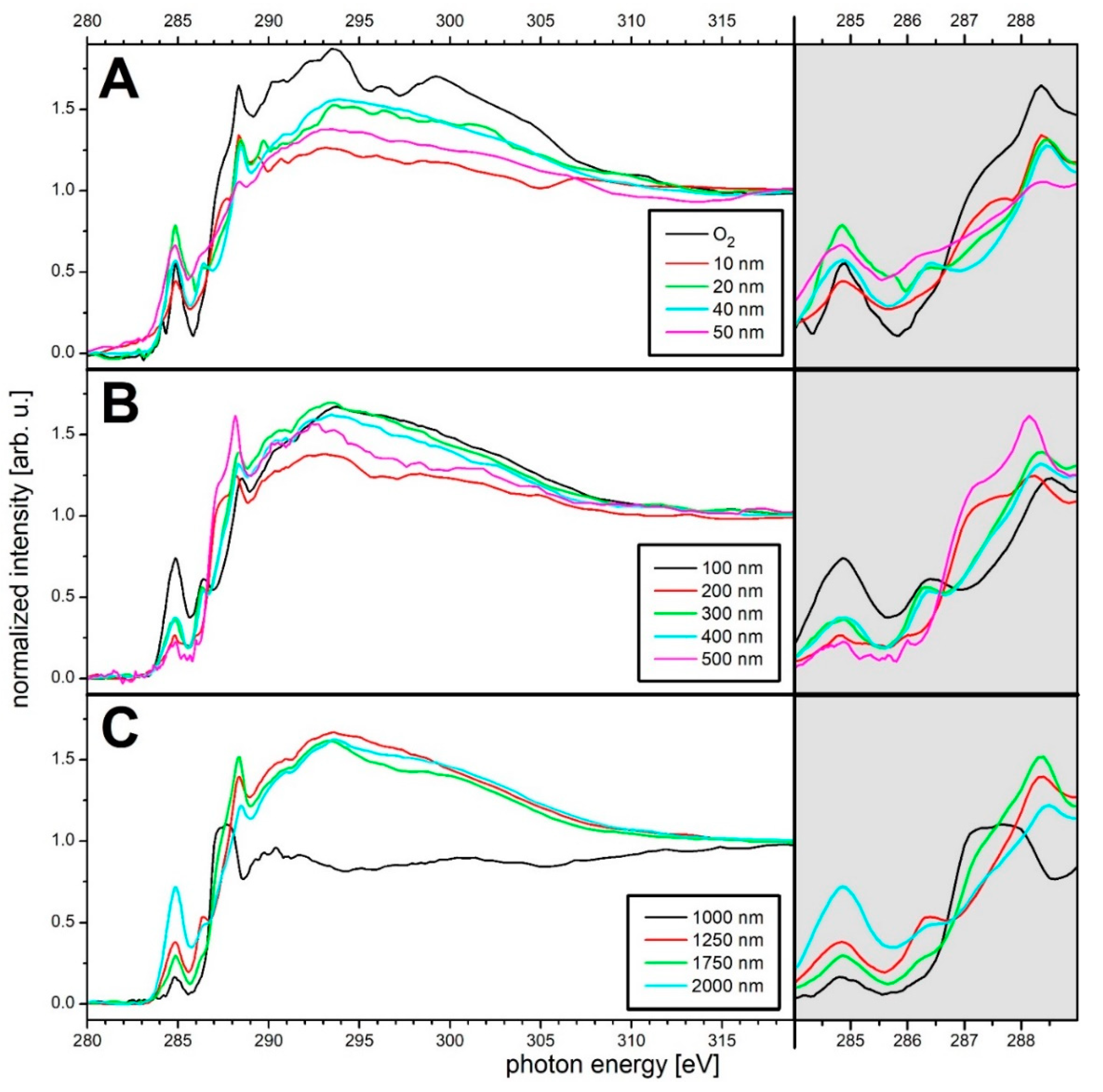
2.3. Sample Surface Chemical Composition

The chemical composition of the surface and the near-surface layers were studied by performing X-ray photoelectron spectroscopy (XPS) and near-edge X-ray absorption fine structure (NEXAFS) measurements at the synchrotron BESSY II, Helmholtz Zentrum Berlin. The measurements were performed during the low-alpha phase to avoid beam damage and strong charging at the sample surface. The HE-SGM beamline was used, which is described in detail elsewhere [30]. The beamline is equipped with an extra electron gun to compensate for beam-induced charging effects on the sample surfaces, which are still present during the low-alpha phase. Both techniques are used to investigate the carbon bond states present at the surface/near-surface region.
The XPS investigations were divided into two steps. First, a full spectrum (survey) from 0 to 700 eV was measured to study the overall chemical composition of each sample’s surface. Subsequently, the C1s peaks were analyzed in detail and evaluated with CasaXPS (software version 2.3.18, Casa Software Ltd., Teignmouth, UK). For the analysis, the C1s peaks were placed at 284.8 eV to compensate for any static charge present [31]. The fractions of sp2, sp3, C‒O and C=O bonds in the total C1s peak were determined via peak deconvolution. When plotting in the final diagram, the C=O bonds were evaluated as sp2 bonds and the C‒O fractions as sp3 bonds. To ensure the homogeneity of the sample surfaces and to check correctness, the measurements were repeated in at least two locations on the surface.
During the NEXAFS studies, both the C K-edge and the O K-edge were measured on the sample surfaces. The O K-edge was used to check the samples for the presence or absence of oxygen on the surface. The measurement of the C K-edge was also repeated in at least two locations to ensure correctness. The angle between the sample and the detector was 55° during the measurements. The measurements were realized in partial electron yield (PEY). A counter voltage was applied to the detector and not all electrons emerging from the sample surface during the X-ray irradiation reached the detector. Only electrons that have exited close to the surface have the necessary energy to reach the detector, and the measurement is therefore very surface-sensitive [30]. The C K-edge was evaluated according to Watt et al. [32] using the commercial software Origin 8.1. Further investigations of the spectra were then performed with a self-written peak-evaluation program.

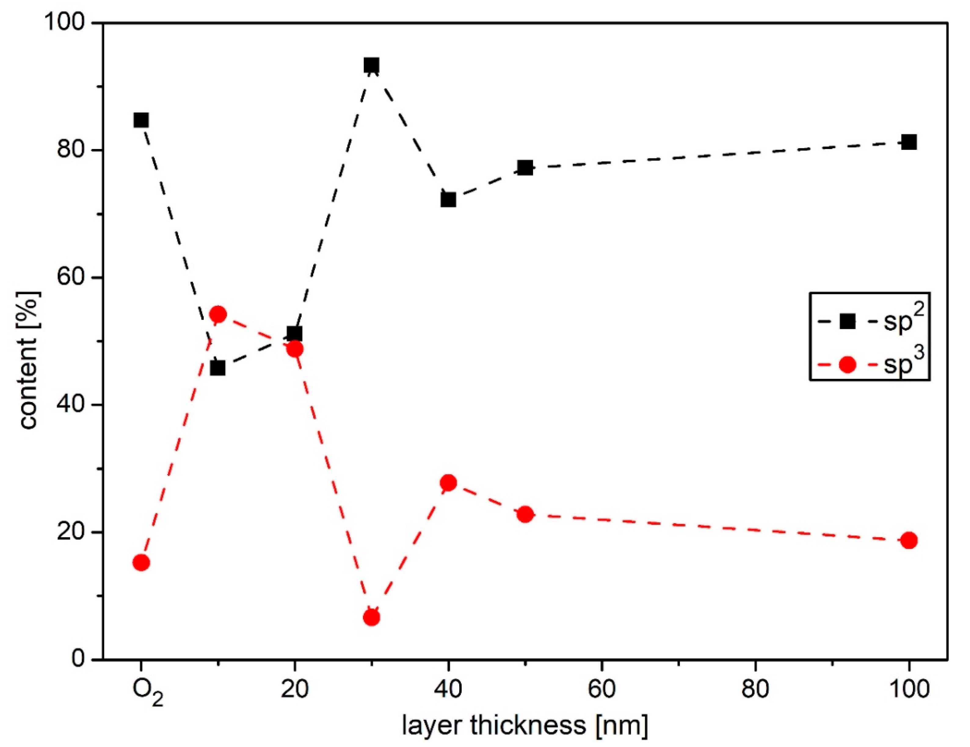
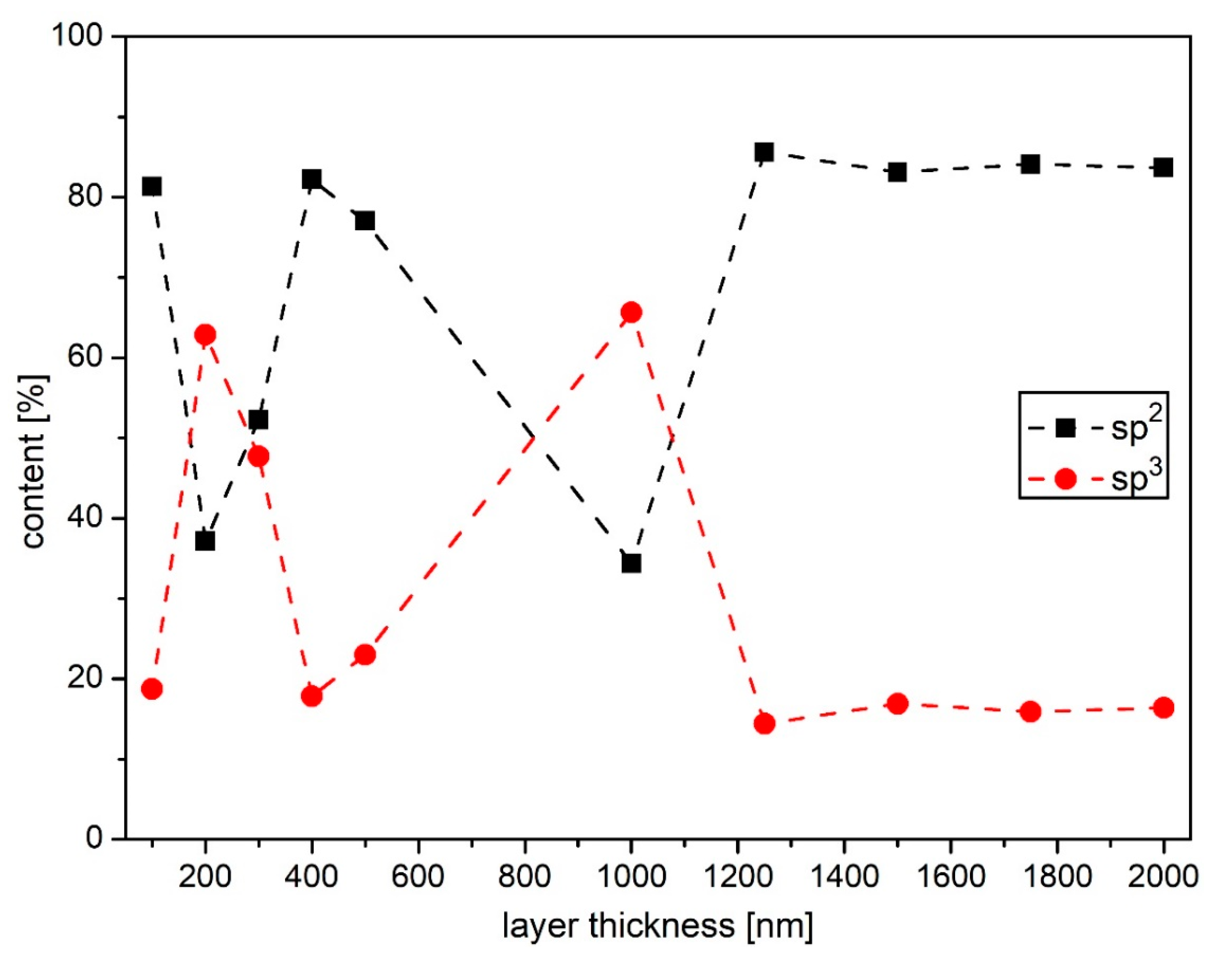
3. Results and Discussion

SEM measurements were performed to verify the condition of the coatings. The results for the range of thin films (up to 100 nm) are displayed in Figure 1. Shown are the oxygen plasma-treated sample (a), the films of 10–50 nm a-C:H thickness in 10 nm steps (b-f) and the 100 nm a-C:H film (g). There were no changes in the state of the deposited layers between 50 and 100 nm.
The O2-treated sample in Figure 1a shows a smooth, clean surface. Only a few particles are visible on the surface. When a 10 nm a-C:H layer was applied (Figure 1b), a homogeneous, closed layer was formed. With increasing layer thickness, this behavior remained unchanged (Figure 1c,d). When the a-C:H layer reached 40 nm, the sample showed many trace-like structures in the SEM. This was probably due to a scratched surface of the sample during production. A reorganization of the layer would also be conceivable (e.g., stress-induced [33]), but the structures were probably too directional for this. Both the 50 and 100 nm samples (Figure 1f,g) had homogeneous, closed layers.
The SEM measurements of the thicker layers are shown in Figure 2, starting with 200 nm a-C:H layer thickness (Figure 2a). The homogeneous, closed surface already observed for the 100 nm sample continued for the 200 and 300 nm samples (Figure 2b). However, the deposition of a 400 nm thick a-C:H layer led to a layer failure on PC. In Figure 2c, the cracks that run through the film are clearly visible. This was most likely due to excessive stress in the film. These stresses occur when there is a high proportion of sp3 bonds in the system [34,35]. When they reach a critical value, the system ruptures and the stress is released. For 500 nm a-C:H on PC (Figure 2d), the layer was again homogeneous and closed (=stable). This held up to a film thickness of 800 nm (not shown here). At 900 nm (Figure 2e), however, the system was again unstable. That layer also cracked due to stress. From a film thickness of 1000 nm (Figure 2f), the film remained closed and homogeneous up to 2000 nm (Figure 2j).
Figure 3 shows the three-dimensional images of the AFM measurements. The respective values for the roughness are given in Table 1. The O2 treated sample (a) was relatively smooth with a roughness Ra of 2.069 nm, but the surface contained particles already visible in the SEM. With the application of a 10 nm a-C:H layer, the surface remained homogeneous. At 20 nm (c) a granular structure was formed. The formation of these grains is a sign that the interlayer phase is completed and normal a-C:H growth begins [5,8]. At 30 nm thickness (d) the most homogeneous surface was present (Ra of 0.789), and only single, small particles were visible. One a-C:H layer was most likely just completed and the next one was beginning to form. The same was applicable to the sample with 50 nm layer thickness (f), but the process was already more advanced.
Figure 4 shows the results of the AFM measurements for layer thicknesses from 200 nm (a) to 2000 nm (i). The corresponding roughness values are listed in Table 1. For 200 nm a-C:H film thickness (Figure 4a), multiple but small grains are visible. At the thickness of 300 nm (b), the number of grains decreased just slightly, but they increased strongly in size. The situation was similar for the 400 nm layer thickness (c). Relatively fewer and smaller grains were on the 500 nm layer (d). The 1000 nm sample (e), like the 2000 nm sample (i), was hardly occupied by grains. The 1250, 1500 and 1750 nm layers showed pronounced grain structures, although of varying intensity (f–h).
The XPS results for thin a-C:H layers on PC are shown in Figure 5. The percentages of sp2 and sp3 binding after deconvolution of the C1s peak with CasaXPS are plotted against the layer thickness in nanometers. The positions of the peaks were determined with the help of the NIST database and from other sources [19,20,36,37,38]. For the plot, the C‒O bonds were counted as sp3 bonds and the C=O bonds as sp2 bonds. The respective values for the whole XPS measurements are shown in Table 2. The relatively high oxygen content of some of these layer surfaces is probably due to saturation of still active bonds on the surface, which occurs after plasma treatment when the vacuum chamber is vented with ambient air. Due to the relatively high surface sensitivity, the saturation of the remaining surface bonds has a great influence on the measurement results obtained. The saturation of broken bonds by internal stress in the layers is also possible. The analysis of the thin layers in 10 nm steps is essential to determining the interlayer thickness. For the O2 plasma-treated raw polymer, 15% sp3 bonded and 85% sp2 bonded carbon were deduced. By depositing an a-C:H layer on PC, the sp3 fraction increased and dominated the carbon network with a fraction of 55%. When a layer thickness of 20 nm was reached, the sp2 and sp3 bonds were balanced. As the a-C:H thickness increased further, the layer behavior changed drastically. The network was strongly sp2 dominated (95%), and the sp3 bonding disappeared almost completely. In the AFM images, the pure layer growth on the surface was also visible (Figure 3c,d). The fraction of sp2 bonds was low with a layer thickness of 40 nm, but remained highly a-C:H dominated (70–80%) up to a layer thickness of 100 nm. Based on the strongly changing layer behavior in the XPS measurements, the interlayer thickness was estimated to be about 20 nm.
The results of the XPS measurements for the thick a-C:H layers deposited on PC begin at a thickness of 100 nm and are plotted in Figure 6. The dominant bond changed briefly to sp3 (63%) at a film thickness of 200 nm. As the film thickness increased, the proportion of sp2 bonds increased again at the expense of the sp3 bonds, and again reached over 80%. In the course of further coating, the proportion of sp2 bonds decreased again until at a film thickness of 1000 nm, the sp3 bond again dominated. The proportions retained were similar to those at 10 and 200 nm. As before, the quantity of sp3 bonds decreased again with increasing film thickness. After reaching an a-C:H layer of 1250 nm, the two bonds remained almost constant up to a film thickness of 2000 nm. After 1250 nm, the a-C:H growth of the film changed compared to the previous behavior. The strongly reduced proportion of sp3 bonds was due to dehydration of the layer. In this process, hydrogen leaves the layer and lowers the amount of sp3-bonded carbons. The free bonds are converted into sp2 hybridized carbons. Thus, re-hybridization of the carbon atom orbitals occurs. This behavior has already been observed for several polymers coated with a-C:H [8,28,29]. Figure 7 presents exemplary deconvolutions of the 10, 100 and 1000 nm a-C:H layer thicknesses for the C1s peak using CasaXPS.
A striking feature is the almost periodic behavior of the carbon bonds over the layer thickness. The sp2 bond dominated, and in a short film thickness interval the sp3 bond was dominant. With each step, however, the proportion of sp3 bonds increased slightly (55%, 63% and 65%). After the sp3 bond was dominant for a short time, the bond ratio suddenly changed to a strongly sp2 dominated carbon network. A comparison with SEM images shows that this change of the dominant bond was accompanied by layer failure. The first change occurred at 20 nm film thickness (Figure 5). With a short delay, no layer failure occurred at 40 nm, but the sample surface was covered with fine, thread-like structures (Figure 1e). It is possible that the stress caused by the sp3 bonds was not yet strong enough to completely crack the layer. However, it is noticeable that there was a strong C‒O content of 20.79 % (Table 2). It is possible that individual, broken C‒C bonds were saturated with oxygen from the environment. As the layer grew from 300 to 400 nm, the dominant bond changed again from sp3 to sp2. The SEM images for the 400 nm sample (Figure 2c) showed a clear cracking of the layer, which took place shortly after the change of the dominant bond. The same applied to the change to the 900 nm sample (Figure 2e). In the XPS the change took place while reaching 1000 nm a-C:H on the sample—thereby only after the layer failure was visible in the SEM. Most likely the fraction of sp3 bonds had already reached its highest value at 900 nm and at the step to 1000 nm it decreased, which was accompanied with a stress release (=breakup of the layer). Unfortunately, the 900 nm sample was not measurable in the XPS. This change from sp3 to sp2 as the dominant bond with a subsequent layer failure has already been observed for other polymers [19,20,23,29]. The more pronounced the interlayer, the greater the delay. In the case of PC, it is very weak with a thickness of 20 nm, and the crack in the layer follows more or less directly after the change in the dominant bond (XPS: change in bond at 20 nm, SEM striking layer behavior at 40 nm). As revealed for polyhydroxy butyrate, the interlayer is of average strength, ending in a delay of 100 nm [20]; for polybutylene adipate terephthalate the interlayer is very pronounced with a delay of 200 nm between the change and the layer failure. Even after failure of the layer, it continues to adhere to the polymer instead of rolling up [23]. Both polyamide 6 (PA6) and HDPE have very pronounced interlayers (40 nm) [28,29]. In both cases, the bonding ratio is very stable, and the layers only break down at very high layer thicknesses. In the case of PA6, no change from sp3 to sp2 as the dominant bond could be detected. However, at the step to 1500 nm film thickness, there was a very strong drop in sp3 bonds (zone of dehydrogenation), followed by film failure at 1750 nm [29]. For HDPE, there was a change from sp3 to sp2 at 50 nm, but layer failure was only observable at 1000 nm [8,28]. As in previous studies, the change from sp2 to sp3 as the dominant bond had no effect on the integrity of the layer [19,20,23,29].
For further analysis of the chemical composition of the coating surface, NEXAFS investigations were performed. The results of the C K-edge are plotted in Figure 8. The determination of the peak location was based on the work of other groups and specified as follows: C=C π (284.85 eV), C‒H (286.15 eV), C‒C (288.35 eV) and C=C σ (292.55 eV) [39,40,41,42,43]. The spectra were analyzed as described in Section 2.3. The diagram is divided into three different thickness ranges: A includes the 0–50 nm a-C:H layer thicknesses; B includes the layers from 100 to 500 nm; and finally, C layers from 1000 to 2000 nm. For better clarification, there is a zoom of the region from 284 to 289 eV to the right of each. In Figure 8A, it can be seen that the ratio of the C=C π peak to the C‒C peak tended to tilt in favor of the C=C π peak with increasing film thickness. Thus, the sp2 bonding was more pronounced with increasing film thickness at the expense of the sp3 bonding. At 50 nm film thickness, the C–C peak was barely visible at 288.15 eV, and the C=C π was relatively emphasized at 284.85 eV. This is also consistent with the results already observed in the XPS (Figure 5). A new feature is that the C K-edge formed a strong C‒H slope for the layer thicknesses of 20 and 40 nm. These were the thicknesses with the largest numbers of grains on the surface just before the end of the layer. A correlation is clearly visible. When the layer was complete and grains were barely visible, this peak disappeared (Figure 3b,d,f and Figure 8A). The 100 nm a-C:H layer thickness on PC again showed the peak for the C‒H bond (Figure 8B). Again, many grains are visible on the surface in the AFM (Figure 3g). The C=C π peak is strongly emphasized, the C‒C peak only weakly developed. This is again in agreement with the XPS measurements. At 200 and 300 nm the C=C π peak decreased, and the C‒C peak at 288.15 is more pronounced. Already in the XPS measurements, it could be seen that the fraction of sp3 was higher (Figure 6). The flanks of the C-H bond were also recognizable. The AFM images (Figure 4a,b) also showed some grains on the surface of the layer. When reaching the 500 nm layer thickness, the C‒H peak almost disappeared and was hardly recognizable. The AFM image showed here (Figure 4d) only isolated and mostly very small grains on the surface. The C-K edge of the 1000 nm a-C:H layer on PC is plotted in Figure 8C. Unfortunately, the measurement in NEXAFS proved to be extremely difficult, so the curve was plotted here more for the purpose of completeness. The C-C peak seems to be superimposed or broadened by a possible charge, which would make an evaluation very error-prone, so it will not be discussed further, except for the non-existent C-H peak. As expected from the previous results, the AFM image (Figure 4e) hardly shows any grain structures. For the thicknesses of 1250 and 1750 nm (1500 nm was not measurable), the ratios of the C=C π and the C‒C peak were about the same, although both peaks are visible in a defined way. The peak of the C-H bond is also observable, although it is weaker for the larger of the two layer thicknesses (1750 nm). Compared with the AFM images (Figure 4f,h), a decrease in the density of the grains with increasing layer thickness can be seen. Finally, when the film thickness increased to 2000 nm, the ratio again tipped in favor of the C=C π peak at 284.85 eV. In the XPS, on the other hand, the ratio of sp2 to sp3 was almost constant from 1000 nm layer thickness, so the C K-edge result for the 2000 nm a-C:H layer differs here from that of the XPS measurements. In the AFM images hardly any grains are visible for this layer thickness (Figure 4i), and also the C‒H peak is no longer present in the NEXAFS measurements.
Overall, however, the two methods correspond to each other and a correlation between grain density on the layer surface and the formation of a C‒H peak was found on the basis of the AFM measurements. Apart from minor deviations (for example, a somewhat more pronounced C‒H peak would have been expected with a film thickness of 200 nm, Figure 4a), this pattern is confirmed. Thus, with the help of the NEXAFS measurement, conclusions can be drawn about the growth status of the current layer. A possible explanation for the more defined C‒H peak with many grains is the size of the surface that is measured. If the layer is smooth, the total surface area is smaller than if the layer is covered with grains. Since the hydrogens represent the ends of the carbon chains, a larger total surface area means that there are also more ends that are detected.

4. Conclusions

Depositions of a-C:H layers were successfully arranged on the polymer PC in various thicknesses (10–2000 nm). The coating was applied by RF-PECVD with acetylene plasma in a vacuum chamber. The obtained layers were subsequently investigated by SEM, AFM, and synchrotron assisted XPS and NEXAFS. Particular attention was paid to the region from 0–100 nm, where the interlayer is formed, which is responsible for the connection of the layer to the base material. It was determined to be 20 nm thick by XPS and AFM measurements. In the AFM, grains are visible from this thickness onwards, which indicate normal a-C:H growth. The XPS shows a completely changing bonding behavior of the carbon atoms on the surface of the layer, which indicates a change in the growth process.
With the SEM measurements, unstable layer thicknesses could be found, where the layer cracks due to internal stresses (400 nm, 900 nm). If the XPS measurements are considered, it is evident that these layer stabilities immediately follow the change from sp3 to sp2 as the dominant bond in the carbon network. Rigid sp3 bonds break due to internal stress and the carbon atoms reorganize to sp2 bonds. The range of dehydrogenation for the a-C:H layers on PC could be determined by XPS to the thickness range of 1250–2000 nm. Here, hydrogen leaves the layers and formerly sp3 bonded carbon atoms reorganize into a strong sp2 dominated network. The NEXAFS investigations confirm the overall results of the XPS. In addition, a correlation between the number and size of grains on the layer surface and the formation of the C‒H peak in the C K-edge was found. The more the surface is maximized by the grains, the more accentuated is the C-H peak. Since the hydrogen atoms terminate the carbon chains and towards the outside, it is obvious that the larger the surface area, the more C-H bonds are present.
The coatability of PC with a-C:H layers was examined and areas of unstable layer thickness were found. In addition, effects were detected that influence the surface bonding ratio. With these fundamentals, targeted modification of the surface properties, such as the application of a thin, scratch-resistant a-C:H layer for e.g., optical components, is now possible. However, further studies must be performed for respective applications.

Author Contributions

T.S., Y.W. and C.B.F. conceptualized the study, and developed and organized the processes. T.S. prepared the samples and contributed the AFM measurements. T.S. also performed the data acquisition and evaluation of XPS and NEXAFS, evaluation of SEM and AFM results, overall data curation, visualization and wrote the manuscript draft. M.F. and L.B. contributed to the acquisition of synchrotron measurements, XPS and NEXAFS. T.S. and C.B.F. validated the results, and reviewed and edited the manuscript. Both S.W. and C.B.F. contributed in terms of funding acquisition, project administration, supervision and overall guidance in the study. All authors have read and agreed to the published version of the manuscript.

Funding

T.S., L.B. and C.B.F. gratefully acknowledge the financial support (funding agreements BESSY 2: 62 and 145) provided by the Helmholtz-Zentrum Berlin (HZB), Germany.

Data Availability Statement

The data presented in this study are available on request from the corresponding author.

Acknowledgments

The authors thank Heinz Busch (NTTF Coatings GmbH, Rheinbreitbach, Germany) for the possibility of industrial coating of the samples. Additionally, we thank Barbara Hahn, Youssef Benjillali and Mohammed Bentaouit from the University of Applied Sciences Koblenz (Department of Material Analysis, RheinAhrCampus) for the SEM equipment and measurements. We also thank Alexei Nefedov from KIT (Karlsruhe Institute for Technology, Group: Chemistry of oxidic and organic interfaces; X-ray and Electron Spectroscopy at Interfaces) for beamtime support. We thank HZB for the allocation of synchrotron radiation beamtime. The authors thankfully acknowledge the financial support by the Helmholtz-Zentrum Berlin (HZB), Germany.

Conflicts of Interest

The authors declare no conflict of interest.

References

  1. Ibrahim, S.S.; Al Jaafari, A.A.; Ayesh, A.S. Physical characterizations of three phase polycarbonate nanocomposites. J. Plast. Film Sheet. 2011, 27, 275–291. [Google Scholar] [CrossRef]
  2. Kausar, A. A review of filled and pristine polycarbonate blends and their applications. J. Plast. Film Sheet. 2018, 34, 60–97. [Google Scholar] [CrossRef] [Green Version]
  3. Krishnan, A.V.; Stathis, P.; Permuth, S.F.; Tokes, L.; Feldman, D. Bisphenol-A: An estrogenic substance is released from polycarbonate flasks during autoclaving. Endocrinology 1993, 132, 2279–2286. [Google Scholar] [CrossRef]
  4. Wang, Y.; Guan, W.; Fischer, C.B.; Wehner, S.; Dang, R.; Li, J.; Wang, C.; Guo, W. Microstructures, mechanical properties and tribological behaviors of amorphous carbon coatings in-situ grown on polycarbonate surfaces. Appl. Surf. Sci. 2021, 563, 150309. [Google Scholar] [CrossRef]
  5. Catena, A.; Guo, Q.; Kunze, M.R.; Agnello, S.; Gelardi, F.M.; Wehner, S.; Fischer, C.B. Morphological and Chemical Evolution of Gradually Deposited Diamond-Like Carbon Films on Polyethylene Terephthalate: From Subplantation Processes to Structural Reorganization by Intrinsic Stress Release Phenomena. ACS Appl. Mater. Interfaces 2016, 8, 10636–10646. [Google Scholar] [CrossRef] [PubMed] [Green Version]
  6. Grill, A. Plasma-deposited diamondlike carbon and related materials. IBM J. Res. Dev. 1999, 43, 147–162. [Google Scholar] [CrossRef]
  7. Couderc, P.; Catherine, Y. Structure and physical properties of plasma-grown amorphous hydrogenated carbon films. Thin Solid Film. 1987, 146, 93–107. [Google Scholar] [CrossRef]
  8. Catena, A.; Agnello, S.; Rösken, L.M.; Bergen, H.; Recktenwald, E.; Bernsmann, F.; Busch, H.; Cannas, M.; Gelardi, F.M.; Hahn, B.; et al. Characteristics of industrially manufactured amorphous hydrogenated carbon (a-C:H) depositions on high-density polyethylene. Carbon 2016, 96, 661–671. [Google Scholar] [CrossRef]
  9. Mohagheghpour, E.; Rajabi, M.; Gholamipour, R.; Larijani, M.M.; Sheibani, S. Ion beam energy dependence of surface and structural properties of amorphous carbon films deposited by IBSD method on Ni–Cu alloy. J. Mater. Res. 2017, 32, 1258–1266. [Google Scholar] [CrossRef]
  10. Paul, R.; Das, S.N.; Dalui, S.; Gayen, R.N.; Roy, R.K.; Bhar, R.; Pal, A.K. Synthesis of DLC films with different sp2/sp3 ratios and their hydrophobic behaviour. Phys. Rev. B 2008, 41, 055309. [Google Scholar] [CrossRef]
  11. Feng, L.; Li, S.; Li, Y.; Li, H.; Zhang, L.; Zhai, J.; Song, Y.; Liu, B.; Jiang, L.; Zhu, D. Super-Hydrophobic Surfaces: From Natural to Artificial. Adv. Mater. 2002, 14, 1857–1860. [Google Scholar] [CrossRef]
  12. Banerjee, D.; Mukherjee, S.; Chattopadhyay, K.K. Controlling the surface topology and hence the hydrophobicity of amorphous carbon thin films. Carbon 2010, 48, 1025–1031. [Google Scholar] [CrossRef]
  13. Ostrovskaya, L.; Perevertailo, V.; Ralchenko, V.; Dementjev, A.; Loginova, O. Wettability and surface energy of oxidized and hydrogen plasma-treated diamond films. Diam. Relat. Mater. 2002, 11, 845–850. [Google Scholar] [CrossRef]
  14. Piazza, F.; Morell, G. Wettability of hydrogenated tetrahedral amorphous carbon. Diam. Relat. Mater. 2009, 18, 43–50. [Google Scholar] [CrossRef]
  15. Bismarck, A.; Brostow, W.; Chiu, R.; Hagg Lobland, H.E.; Ho, K.K.C. Effects of surface plasma treatment on tribology of thermoplastic polymers. Polym. Eng. Sci. 2008, 48, 1971–1976. [Google Scholar] [CrossRef]
  16. Koidl, P.; Wild, C.; Dischler, B.; Wagner, J.; Ramsteiner, M. Plasma Deposition, Properties and Structure of Amorphous Hydrogenated Carbon Films. MSF 1991, 52–53, 41–70. [Google Scholar] [CrossRef]
  17. Robertson, J. Diamond-like amorphous carbon. Mater. Sci. Eng. R Rep. 2002, 37, 129–281. [Google Scholar] [CrossRef] [Green Version]
  18. Zhou, Y.; Wang, B.; Song, X.; Li, E.; Li, G.; Zhao, S.; Yan, H. Control over the wettability of amorphous carbon films in a large range from hydrophilicity to super-hydrophobicity. Appl. Surf. Sci. 2006, 253, 2690–2694. [Google Scholar] [CrossRef]
  19. Schlebrowski, T.; Beucher, L.; Bazzi, H.; Hahn, B.; Wehner, S.; Fischer, C.B. Prediction of a-C:H layer failure on industrial relevant biopolymer polylactide acide (PLA) foils based on the sp2/sp3 ratio. Surf. Coat. Technol. 2019, 368, 79–87. [Google Scholar] [CrossRef]
  20. Schlebrowski, T.; Beucher, L.; Bazzi, H.; Hahn, B.; Wehner, S.; Fischer, C.B. Changing Contents of Carbon Hybridizations in Amorphous Hydrogenated Carbon Layers (a-C:H) on Sustainable Polyhydroxybutyrate (PHB) Exhibit a Significant Deterioration in Stability, Depending on Thickness. C 2019, 5, 52. [Google Scholar] [CrossRef] [Green Version]
  21. Robertson, J. Plasma Deposition of Diamond-Like Carbon. Jpn. J. Appl. Phys. 2011, 50, 01AF01. [Google Scholar] [CrossRef]
  22. Lee, S.-C.; Tai, F.-C.; Wei, C.-H. Correlation between sp2/sp3 Ratio or Hydrogen Content and Water Contact Angle in Hydrogenated DLC Film. Mater. Trans. 2007, 48, 2534–2538. [Google Scholar] [CrossRef] [Green Version]
  23. Schlebrowski, T.; Acharchi, H.; Hahn, B.; Wehner, S.; Fischer, C.B. Refinement of Sustainable Polybutylene Adipate Terephthalate (PBAT) with Amorphous Hydrogenated Carbon Films (a-C:H) Revealing Film Instabilities Influenced by a Thickness-Dependent Change of sp2/sp3 Ratio. Materials 2020, 13, 1077. [Google Scholar] [CrossRef] [Green Version]
  24. Fischer, C.B.; Rohrbeck, M.; Wehner, S.; Richter, M.; Schmeißer, D. Interlayer formation of diamond-like carbon coatings on industrial polyethylene: Thickness dependent surface characterization by SEM, AFM and NEXAFS. Appl. Surf. Sci. 2013, 271, 381–389. [Google Scholar] [CrossRef]
  25. Rohrbeck, M.; Körsten, S.; Fischer, C.B.; Wehner, S.; Kessler, B. Diamond-like carbon coating of a pure bioplastic foil. Thin Solid Film. 2013, 545, 558–563. [Google Scholar] [CrossRef]
  26. Neyts, E.; Bogaerts, A.; Van de Sanden, M.C.M. Reaction mechanisms and thin a-C: H film growth from low energy hydrocarbon radicals. J. Phys. Conf. Ser. 2007, 86, 012020. [Google Scholar] [CrossRef]
  27. Catena, A.; Kunze, M.R.; Agnello, S.; Gelardi, F.M.; Wehner, S.; Fischer, C.B. Amorphous hydrogenated carbon (a-C:H) depositions on polyoxymethylene: Substrate influence on the characteristics of the developing coatings. Surf. Coat. Technol. 2016, 307, 658–665. [Google Scholar] [CrossRef]
  28. Schlebrowski, T.; Rouabeh, W.; Wehner, S.; Fischer, C.B. Specifying the interlayer turning point and dehydrogenation in a-C:H layers plasma deposited on high-density polyethylene with X-ray synchrotron techniques. Thin Solid Film. 2019, 691, 137617. [Google Scholar] [CrossRef]
  29. Schlebrowski, T.; Lüber, H.; Beucher, L.; Fritz, M.; Benjillali, Y.; Bentaouit, M.; Hahn, B.; Wehner, S.; Fischer, C.B. Plasma Supported Deposition of Amorphous Hydrogenated Carbon (a-C:H) on Polyamide 6: Determining Interlayer Completion and Dehydrogenation Effects during Layer Growth. Polymers 2021, 13, 1886. [Google Scholar] [CrossRef] [PubMed]
  30. Nefedov, A.; Wöll, C. Advanced Applications of NEXAFS Spectroscopy for Functionalized Surfaces. In Surface Science Techniques; Bracco, G., Holst, B., Eds.; Springer Berlin Heidelberg: Berlin/Heidelberg, Germany, 2013; pp. 277–303. ISBN 978-3-642-34242-4. [Google Scholar]
  31. Fang, D.; He, F.; Xie, J.; Xue, L. Calibration of Binding Energy Positions with C1s for XPS Results. J. Wuhan Univ. Technol. Mat. Sci. Ed. 2020, 35, 711–718. [Google Scholar] [CrossRef]
  32. Watts, B.; Thomsen, L.; Dastoor, P.C. Methods in carbon K-edge NEXAFS: Experiment and analysis. J. Electron. Spectrosc. Relat. Phenom. 2006, 151, 105–120. [Google Scholar] [CrossRef]
  33. Schlebrowski, T.; Ouali, R.; Hahn, B.; Wehner, S.; Fischer, C.B. Comparing the Influence of Residual Stress on Composite Materials Made of Polyhydroxybutyrate (PHB) and Amorphous Hydrogenated Carbon (a-C:H) Layers: Differences Caused by Single Side and Full Substrate Film Attachment during Plasma Coating. Polymers 2021, 13, 184. [Google Scholar] [CrossRef]
  34. Lacerda, R.G.; Marques, F.C. Hard hydrogenated carbon films with low stress. Appl. Phys. Lett. 1998, 73, 617–619. [Google Scholar] [CrossRef] [Green Version]
  35. Marques, F.C.; Lacerda, R.G.; Odo, G.Y.; Lepienski, C.M. On the hardness of a-C:H films prepared by methane plasma decomposition. Thin Solid Film. 1998, 332, 113–117. [Google Scholar] [CrossRef]
  36. Tai, F.C.; Lee, S.C.; Wei, C.H.; Tyan, S.L. Correlation between ID⁄IG Ratio from Visible Raman Spectra and sp2/sp3 Ratio from XPS Spectra of Annealed Hydrogenated DLC Film. Mater. Trans. 2006, 47, 1847–1852. [Google Scholar] [CrossRef] [Green Version]
  37. Solomon, J.L.; Madix, R.J.; Stöhr, J. Orientation and absolute coverage of benzene, aniline, and phenol on Ag(110) determined by NEXAFS and XPS. Surf. Sci. 1991, 255, 12–30. [Google Scholar] [CrossRef]
  38. Dietrich, P.M.; Horlacher, T.; Girard-Lauriault, P.-L.; Gross, T.; Lippitz, A.; Min, H.; Wirth, T.; Castelli, R.; Seeberger, P.H.; Unger, W.E.S. Adlayers of dimannoside thiols on gold: Surface chemical analysis. Langmuir 2011, 27, 4808–4815. [Google Scholar] [CrossRef]
  39. Stöhr, J. NEXAFS Spectroscopy; Springer: Berlin/Heidelberg, Germany, 1992; ISBN 978-3-662-02853-7. [Google Scholar]
  40. Brüster, B.; Amozoqueño, C.; Grysan, P.; Peral, I.; Watts, B.; Raquez, J.-M.; Dubois, P.; Addiego, F. Resolving Inclusion Structure and Deformation Mechanisms in Polylactide Plasticized by Reactive Extrusion. Macromol. Mater. Eng. 2017, 302, 1700326. [Google Scholar] [CrossRef]
  41. Díaz, J.; Anders, S.; Zhou, X.; Moler, E.J.; Kellar, S.A.; Hussain, Z. Analysis of the π* and σ* bands of the x-ray absorption spectrum of amorphous carbon. Phys. Rev. B 2001, 64, 125204. [Google Scholar] [CrossRef]
  42. Dhez, O.; Ade, H.; Urquhart, S.G. Calibrated NEXAFS spectra of some common polymers. J. Electron Spectrosc. Relat. Phenom. 2003, 128, 85–96. [Google Scholar] [CrossRef]
  43. Diaz, J.; Monteiro, O.R.; Hussain, Z. Structure of amorphous carbon from near-edge and extended x-ray absorption spectroscopy. Surf. Coat. Technol. 2007, 76, 094201. [Google Scholar] [CrossRef]
Figure 1. SEM images for the thin a-C:H layers on PC. Shown are the O2-treated PC sample (a); a-C:H deposited in thicknesses from 10 to 50 nm (bf) and 100 nm (g).
Carbon 07 00059 g001
Figure 2. SEM results for thick a-C:H layers deposited on PC. Shown are the film thicknesses of 200 nm (a) to 2000 nm (j).
Carbon 07 00059 g002
Figure 3. AFM 3D-images for the O2 plasma-treated PC sample (a) and PC coated with thin a-C:H layers from 10 nm (b) to 100 nm (g).
Carbon 07 00059 g003
Figure 4. AFM 3D-images for PC samples coated with thick a-C:H layers from 200 nm (a) to 2000 nm (i).
Carbon 07 00059 g004
Figure 5. XPS results for thin a-C:H layers on PC. The sp2 content (black squares) and sp3 (red circles) bound carbon are plotted against layer thickness (dashed lines show only a trend).
Carbon 07 00059 g005
Figure 6. XPS results for thick a-C:H layers deposited on PC, up to 2000 nm. The black squares are the sp2 content and the red circles are the sp3 bound carbons plotted against layer thickness (dashed lines only show a trend).
Carbon 07 00059 g006
Figure 7. Exemplary XPS peak deconvolution for the a-C:H layer thicknesses of 10, 100 and 1000 nm. The analysis was performed on the sp2, sp3, C-O and C=O fractions using CasaXPS software.
Carbon 07 00059 g007
Figure 8. NEXAFS C K-edge spectra for a-C:H layers of various thicknesses deposited on PC. (A) The a-C:H thicknesses 0–50 nm, (B) 100–500 nm and (C) 1000–2000 nm. On the left are the full spectra (280–320 eV); on the right is a magnification of the region from 284 to 289 eV. Here are the peaks located for C=C π (284.85 eV), C‒H (286.15 eV) and C‒C (288.15 eV).
Carbon 07 00059 g008
Table 1. AFM roughness values Ra and Rq: analyzed are the O2 plasma-treated PC sample and PC samples coated with a-C:H layers of various thickness in ascending order.
SampleRa
[nm]
Rq
[nm]
O22.069 ± 1.5785.256 ± 15.320
102.759 ± 2.0954.775 ± 5.086
202.363 ± 0.4012.999 ± 0.649
300.789 ± 0.2401.350 ± 0.581
403.812 ± 0.7194.932 ± 1.091
502.940 ± 1.7445.155 ± 2.925
1005.161 ± 1.3837.140 ± 2.134
2004.978 ± 1.3816.946 ± 2.162
3005.729 ± 3.5859.890 ± 6.357
4003.850 ± 1.9686.783 ± 3.564
5002.048 ± 1.3953.886 ± 3.613
10007.443 ± 7.51915.250 ± 16.670
12504.546 ± 1.4546.432 ± 2.398
15003.790 ± 1.0805.161 ± 2.387
17503.460 ± 1.2744.813 ± 2.868
20002.139 ± 1.1894.331 ± 2.745
Table 2. Results of XPS measurements separated into the percentages of sp2, sp3, C‒O and C=O binding to the C1s peak after deconvolution.
Samplesp2
[%]
sp3
[%]
C-O
[%]
C=O
[%]
O283.494.5510.701.26
1042.5538.5915.650.37
2048.5843.425.382.63
3090.144.242.393.24
4072.197.0220.790.00
5074.5812.979.842.62
10079.3911.437.291.90
20034.0248.8114.043.12
30051.7735.4412.260.53
40080.514.0513.761.69
50068.1022.990.008.91
100023.6350.6814.9610.73
125084.9514.400.000.65
150083.1216.880.000.00
175082.9410.705.201.17
200082.580.3116.061.05
Publisher’s Note: MDPI stays neutral with regard to jurisdictional claims in published maps and institutional affiliations.

