1. Introduction
Printed circuit boards (PCBs) are essential components of many contemporary electronic systems, ranging from private sector computers and cell phones to public sector military and medical equipment. Predominant developments in the outsourcing of PCB manufacturing make boards increasingly vulnerable on a global scale to malicious changes from external entities [
1]. Attacks such as hardware Trojan insertions provide backdoor access to sensitive networks and compromise a nation’s infrastructure, military capability, and civil safety. Therefore, PCB assurance is an important research area in cyber-security.
With the PCB supply chain being potentially highly unreliable and insecure, the US government has taken multiple steps to bring changes to the protocols [
2,
3]. However, assurance is limited by the lack of automatic inspection methods. Reference [
2] reports that apart from integrated circuits (ICs), resistors, capacitors, and transistors are among the most commonly counterfeited components, these being the most predominant of electronic components on any given PCB; it is, therefore, essential to identify and validate these components in any PCB.
Over the years, many state-of-the-art approaches for automated PCB assurance have been developed using image processing, computer vision, and machine learning in the visual spectrum [
4,
5,
6]. However, most of these approaches often need a golden sample, i.e., a PCB proven free of flaws and hardware Trojans, to compare with the device under test (DUT). These golden references are often not available in areas such as hardware assurance reverse engineering. Hence, certain approaches that can operate in their absence must be developed, such as bill of materials (BoM) analysis.
A BoM is a list of all components on a PCB, such as resistors, capacitors, and integrated circuits (ICs) [
7]. BoM analysis, i.e., contrasting the BoM collected from the DUT and the BoM published by the design firm, can reveal out-of-spec, defective, reused, recycled, and malicious board alterations without the presence of a golden sample. BoMs have several uses outside the area of hardware assurance as well, such as reverse engineering (e.g., foreign, competitor, or legacy device analysis), industrial assessments (e.g., cost estimation, quality assurance), and academic research (e.g., technology trend analysis) [
8]. Toward this end, we developed AutoBoM, which is a framework for automatically extracting a BoM using optical images of a target PCB [
9].
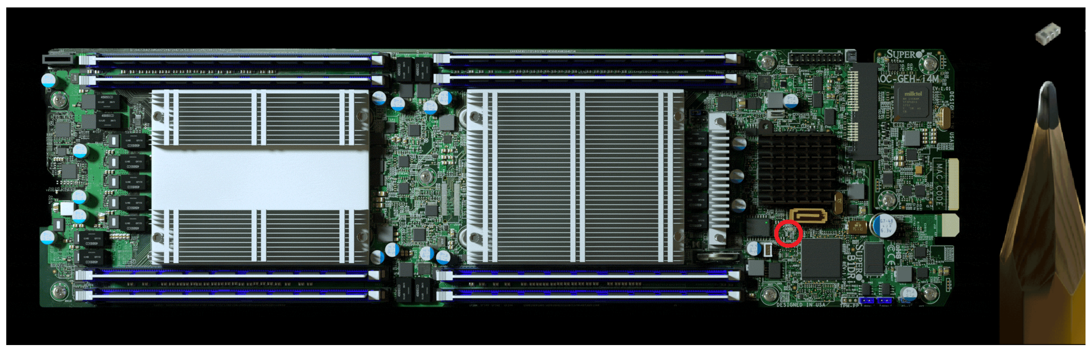
For a successful and fully automated bill of materials extraction, several conditions must be met. Firstly, there are a various types of components on a board (resistors, capacitors, sensors, ports, potentiometers, inductors, etc.), so it is important to classify them into different types, and extract the peripheral information necessary to identify them correctly. For example, resistors can be identified by their resistance values and ICs can be identified by their model and part numbers. Second, processing should be performed extremely fast. Due to increased outsourcing and globalization, the electronics supply chain and hardware community span over multiple continents. With so many external entities involved in the PCB life cycle, companies must validate the PCBs quickly to maintain the short time-to-market. Finally, and most importantly, the automatic extraction of a bill of materials must be accurate. Though PCBs consist of hundreds, or even thousands of components, the addition, removal, or substitution of a single component could compromise the confidentiality, integrity, and/or accessibility of the entire system. An exemplary case is presented in
Figure 1. Though the claims in [
10] are under dispute, many experts in the hardware assurance community agree that the claims are highly plausible, and it is only a matter of time before more such reports surface. Since PCBs are often mass-produced for critical government, military, and biomedical infrastructures, 100% accuracy is highly desirable.
Numerous object detection approaches still cannot achieve near 100% accuracy on popular million-image datasets [
11,
12]. There is a trend of showcasing increasingly better performance either in speed or in accuracy over the other popular architectures, but the focus has not been on pushing toward attaining perfect accuracy for any one particular scenario [
13,
14], predominantly because this is not the focus. Automatic bill of materials extraction, being a special case of object detection, has not seen as a solution either even with innovative machine learning (ML) and deep learning (DL) techniques. Due to the inherent uniqueness of the PCB assurance field, such a solution is even more challenging and there is still much progress and collaboration needed from the hardware assurance and security community for automated, accurate, and scalable PCB component recognition.
Our contributions in this study are as follows: (i) an investigation of ML and DL challenges in the PCB assurance domain, (ii) an introduction of our proposed ECLAD-Net, a specialized network for PCB component detection, and (iii) a comparison of the benefits and limitations of the proposed method and those of other popular object detection methods. The rest of the paper is organized as follows. In
Section 2, the challenges for automated PCB assurance are elaborated. Then, in
Section 3 and
Section 4, existing techniques along with a novel method, the electronic component localization and detection network (ECLAD-Net), are presented.
Section 5 compares the proposed method with the existing methods. Finally,
Section 6 concludes the paper with future work needed to enhance the hardware assurance community.
2. Challenges for Automatic PCB Assurance
There are several elements of PCBs that present challenges for component recognition and are hence difficult for existing algorithms to tackle. The following subsections elaborate on the challenges of (i) high intra-class/low inter-class variance, (ii) the evolving problem scope, and (iii) a limited amount of data.
2.1. The Variance Problem
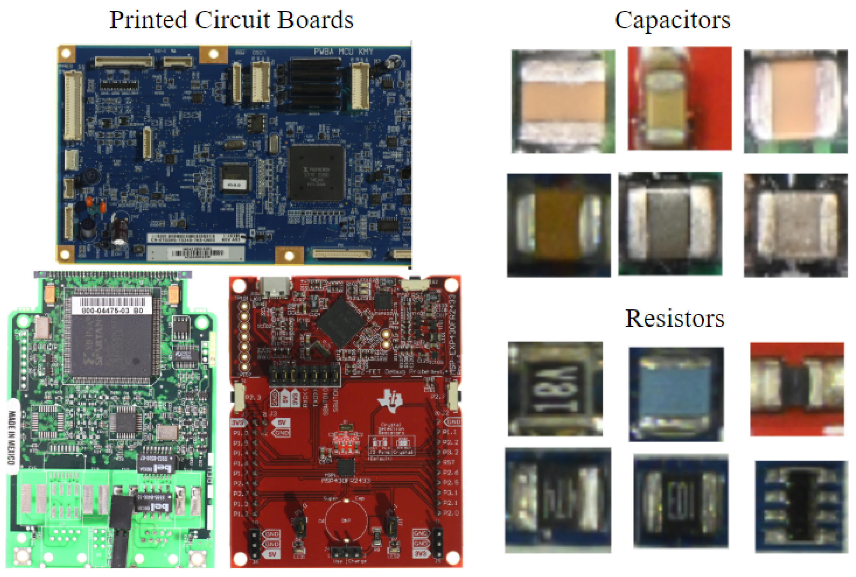
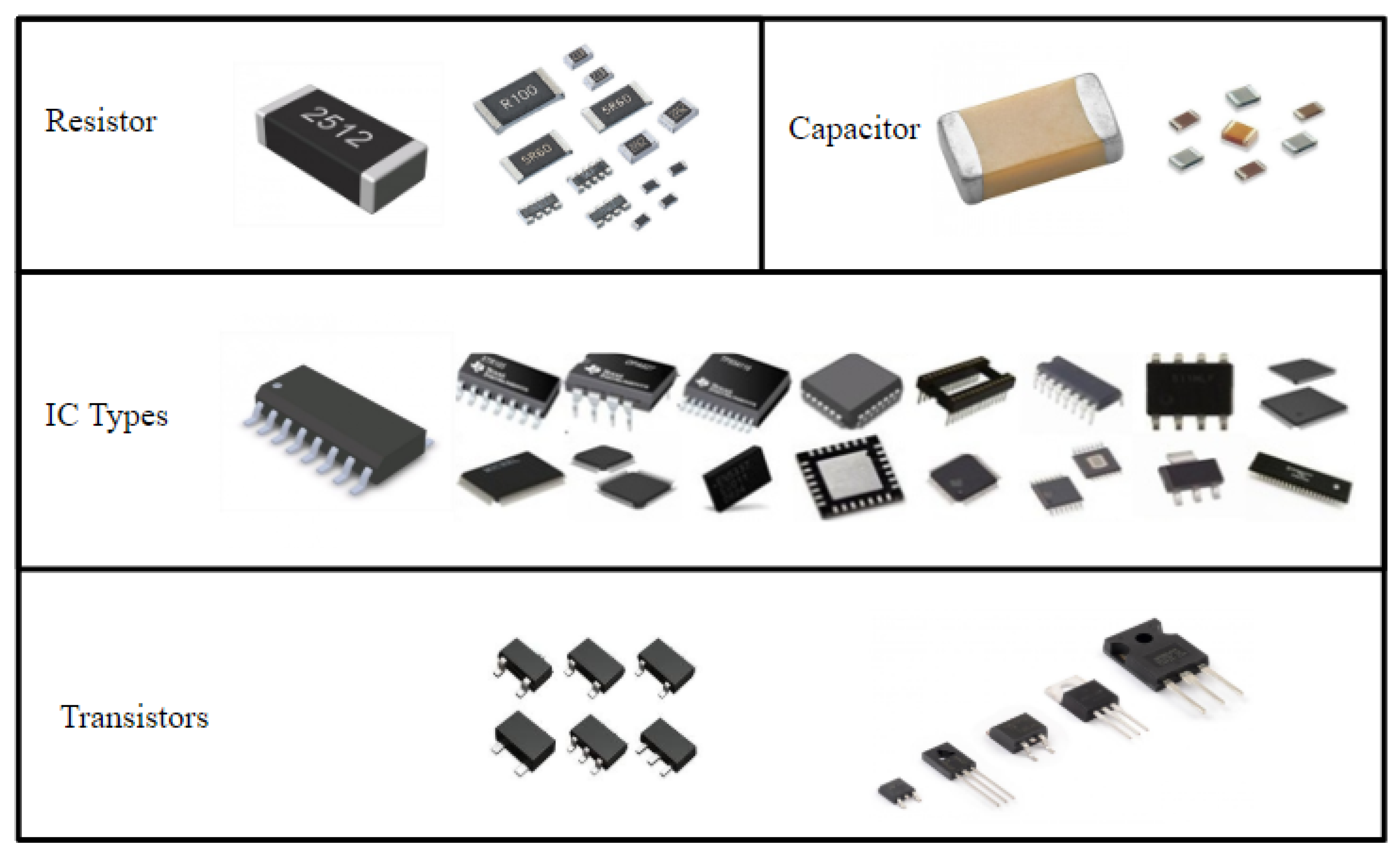
PCBs are comprised of several different types of components. Examples of four common types are presented in
Figure 2. As shown, there are examples of the same component type that appear different (high intra-class variance) and examples of different component types that appear similar (low inter-class variance). There are also many other types of components that further complicate the variance problem not shown in
Figure 2, including but not limited to, inductors, transformers, and crystal oscillators. At present, there is a lack of universal standards for classifying the different component types (e.g., a resistor network array could be categorized as a resistor, an IC, or as a class all by itself).
In addition, there are numerous other factors that contribute to the variance problem. The PCB board itself may possess component-like features, which could result in false positive detections. Component appearances, functionalities, and classifications may vary by company, year, and even by designer. Components can also change over time, as they age naturally with standard wear-and-tear. Additionally, the majority of modern PCB components are machine-placed off-the-shelf surface mount device (SMD) resistors and capacitors. Such a class imbalance must be accounted for when training and evaluating component recognition algorithms. In addition, since the input image is an optical image, there are also non-PCB factors contributing to the variance problem, such as imaging condition (e.g., lighting, angle-of-view, and resolution). These variations present additional challenges for designing a high-accuracy PCB component recognition method.
2.2. Evolving Problem Scope
Technology is in a constant state of development toward smaller components which enables a higher level of complexity with more compact designs at the PCB level, from small single-board microcontrollers to large motherboards and GPUs [
10]). Additionally, just as PCB designs are becoming more advanced, so too are hardware Trojans and the protective coutermeasures against them. Not only is there a variance challenge (as described in
Section 2.1), but the aforementioned problem is regularly changing over time.
The constantly evolving nature of the PCB assurance problem and its scope presents challenges for traditional image processing and computer vision approaches, which operate best in closed systems [
15]. Hence, intelligent algorithms capable of learning (i.e., ML and DL) are necessary to achieve and maintain high accuracy and avoid becoming outdated.
2.3. The Need for a Dataset
As stated in
Section 2.2, the PCB assurance problem is highly dynamic, so ML and DL are vital. This requires a large and regularly updated dataset of images labeled by subject matter experts (SMEs). Though there are several existing datasets of PCB components, there are few that are publicly available [
16]. Moreover, many of the available datasets are intended and formatted for a specific study, so they are difficult to combine effectively and re-purpose for a different study. For example, FICS-PCB [
16] consists of 9900 images taken with a Digital Single-Lens Reflex (DSLR) camera and optical microscope with six component classes annotated, and PCB-Metal [
17] consists of only 1000 images taken with a DSLR camera with four component classes annotated. While these datasets provide sufficient information to experiment with various algorithms, much work is needed to increase and maintain data to be representative of as many components and their variations as possible.
Meanwhile, PCB assurance is currently a field with a large number of classes and a relatively small amount of data per class. ML and DL methods, which tend to require large amounts of data, tend to overfit (i.e., overtrain) when trained on such a limited datset. Overfitting, which is when a ML model is memorizing instead of learning salient features necessary for recognition, can be identified by significant performance degradation between training and testing accuracy. There are two primary ways to prevent overfitting: (1) collect more data or (2) use prior knowledge (e.g., PCB design rules) to reduce the number of free parameters so the amount of data required by the ML model is reduced. Both ways require much work and collaboration from the hardware assurance community to standardize the way data and prior knowledge is collected, annotated, and communicated.
To summarize, there are several object detection challenges in the PCB assurance domain. Hence, conventional approaches will be limited, as they are not tailored to the specific problem. In the following sections, we evaluate several of these conventional approaches, present a novel method, and compare them.
3. Related Work
Within the PCB assurance field, the majority of existing work has focused on defect detection. For example, [
18] proposes a placement defect detection approach using genetic algorithms while [
19] proposes an approach using SURF and conventional morphological operations. A comprehensive survey of old and new hardware defect detection approaches can be found in [
1,
4]. In such methods, “defects” are defined in reference to a golden, i.e., non-defective, sample. Counterfeiters and adversaries intentionally obscure designs to make detection difficult, but golden samples may not be always available. In addition, general analysis of a PCB to localize and extract regions using image segmentation techniques are presented in [
20]. Similarly [
21,
22] present approaches using features based detection (e.g., color, illumination, background, and tilted objects), however they address specific problems and not PCB assurance as a whole. Hence, alternative methods such as Automatic bill of materials extraction have been proposed as an additional hardware assurance method, complimentary to defect detection.
Automatic bill of material extraction is an application of object recognition, the process of detecting and identifying objects. Recognition can be categorized into two types: (i) regression and (ii) classification. The main difference is regression returns a continuous number (e.g., a confidence percentage such as an object is 78% capacitor vs. 22% resistor) while classification returns a discrete value (e.g., this object is most like a capacitor). Classification can be considered a special case of regression, in that a decision criteria is used to group the detected objects into preexisting categories (classes). In this study, the classification is considered for further analysis.
Over the years, numerous generic object recognition techniques have been proposed [
23]. For example, popular two stage methods (e.g., RCNN [
24], and FastRCNN [
25]) and single stage detectors (e.g., YOLO [
26] and SSD [
27]) have all demonstrated high accuracy on popular datasets [
23]. However, due to the inherent uniqueness of the PCB assurance field (as explored in
Section 2), there is still much research is needed in this area.
Only recently have there been applications of ML and DL for PCB component recognition. Reference [
28] proposes a conventional machine learning based approach using an AdaBoost classifier to detect capacitors. Here, the proposed method focuses only on through hole capacitors, which are easier to detect and are less common on modern PCBs than the SMD variety. Lately, there have been a few DL methods investigated for PCB component detection such as [
29,
30]. Reference [
29] conducted a thorough analysis using the YOLO architecture and found Average Precision(AP) scores for capacitors and resistors at only about 50%. In [
30], which uses an object detection with a graph-based neural network to recognize multiple PCB component classes, a similar poor performance is observed for smaller components such as resistors and capacitors. While both of the latter approaches appear to detect large components such as ICs, ports and those will high interclass variance, these struggle for smaller low interclass variance samples. From these works, it appears the challenges in PCB component detection are such that generalized techniques are not sufficient to achieve and maintain high accuracy. Hence, we propose a more specialized method, the electronic component localization and detection network (ECLAD-net) in the following section.
4. Materials and Methods
To reiterate, the goal of this paper is to present the need for specialized Artificial Intelligence (AI) for PCB hardware assurance. To this end, several generic object recognition methods from literature are explored. Then, we propose a novel specialized method: ECLAD-net, and compare its performance with those of the existing solutions.
Analysis is conducted in two phases: (i) classification and (ii) detection. Though the ordering of the phases appear counter-intuitive to traditional two-step detection-then-classification approaches, this is done on purpose to showcase the specific challenges associated with each step, independent of each other. In phase (i), we compare classifiers popular in literature with ECLAD-net’s object classification stage using manually cropped resistors and capacitors. This experiment is conducted with such controlled conditions to investigate the feasibility of the tested classification methods, independent of any detection stages. In phase (ii), we compare object detection methods popular in literature with ECLAD net’s object detection stage using entire PCB images, with the goal to detect resistors and capacitors. Comparing only the detectors make it difficult to identify at what stage the error is from, thus making the classification phase necessary. Results are discussed in
Section 5.
4.1. Experiment Specifications
The objective of the following experiments is to introduce and compare the performance of the novel ECLAD-net with those of popular approaches for the tasks of classifying and detecting resistors and capacitors. While there are other classes of components such as ICs, inductors; Resistors and capacitors succinctly capture the structure, color palette, and texture of the majority of components within a PCB. Results obtained using these two classes are sufficient to describe the complications in PCB component recognition.
Two datasets were used for the experiments in this study. For the component classification analysis, from 1152 images, 1000 images of manually cropped and labeled resistors and capacitors were used (to maintain class-balance). Data augmentation was used to increase the number of images to reduce overfitting of larger networks; more detail is discussed in the
Section 4.2 and
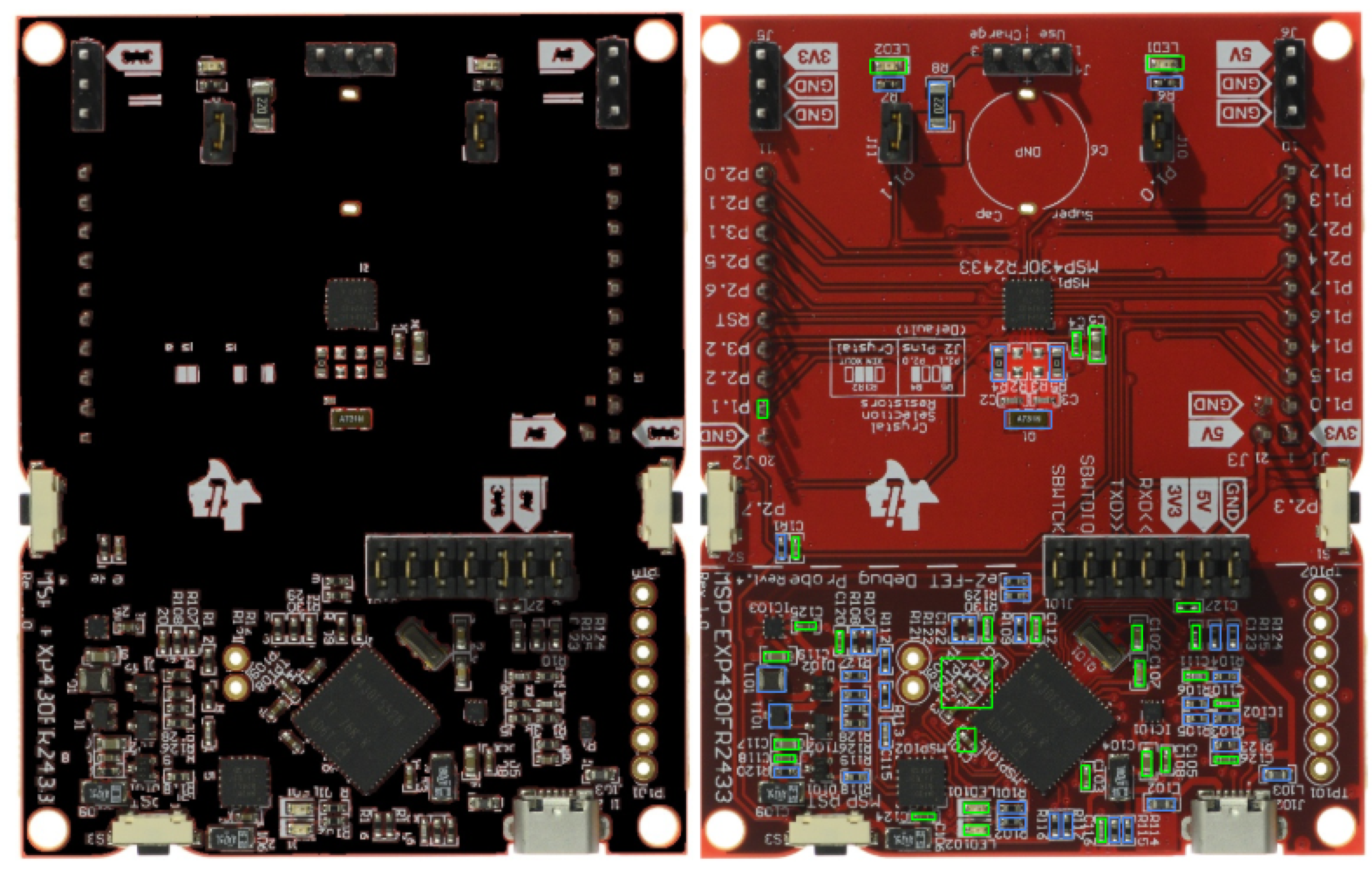
Section 4.3. For the component detection analysis, 26 three-channel RGB images of PCBs were also used. The PCB images were collected with a high-resolution (i.e., 5000 pixels × 4000 pixels, on average) DSLR camera, collected in a top-down fashion using a vertical mount setup.
Table 1 presents statistics of the dataset used and
Figure 3 presents examples of the datasets. Images were captured under moderate lighting conditions to reduce reflection from the different PCB materials. Image clarity is verified by computing the signal-to-noise ratio (SNR). PCBs are iteratively imaged until a clear, high resolution image, i.e., an image with a high db psnr, is obtained, relative to every sample imaged. Experiments were performed in python using libraries such as Keras, Opencv, Scikit-image, Scikit-learn, and Tensorflow. Where implementation of existing method is available, we have utilized them for comparison purposes. The code was run on a core i5 desktop with 4 GB of Nvidia 1050-Ti GPU.
4.2. Classification of Resistors and Capacitors
Before discussing the challenges of PCB component detection, classification of resistors and capacitors is first investigated to establish if the problem is feasible. Here, high intra-class/low inter-class variance is a key challenge. Hence, these classification experiments indicate class separability in the low- and high-dimensional spaces.
When training in higher-dimensional spaces, more data is required. Here, data augmentation was used to increase the dataset by a factor of 8. Augmentations were chosen to be realistic, i.e., representative of real-scenario variances. For instance, the capacitor and resistor images were rotated by 90, 180, and 270. These values were chosen as realistic because pick-and-place assembly devices primarily implant SMD components horizontally or vertically with high precision and mild deviation. Additional augmentations include random image cropping with a maximum of 25% to encourage algorithm generalizability and regularization.
Additionally, before classification, images are normalized by scaling data to possess zero mean and unit variance. The dataset, which consisted of 8000 images after augmentation, was split 80%:20% into training and testing sets. The training data was further split 80%:20% for validation testing. Data was split to maintain balanced classes. When possible, 3-fold cross validation is performed. The loss function, optimization algorithms, and other algorithm-specific parameters vary by the method employed, and will be discussed in the following subsection.
4.2.1. Previous Classifiers from Literature
For a baseline, two conventional ML approaches were implemented: the squared error classifier and the hinge linear classifier. For both classifiers, two different models were used: one to model resistors, and the other for capacitors. Images were then classified based on the model that returned the highest confidence (i.e., match score). The hinge linear classifier models, which simulate linear support vector machines (SVMs) by optimizing over hinge loss, were configured as one vs rest. All linear classifier models were trained using stochastic gradient descent for 1500 epochs maximum, with a 10-epoch early stopping condition with an epsilon of 10.
Several standard neural network (NN) approaches of various architectures were explored. Select examples are described below, including two fully-connected dense NNs, two convolutional NN (CNN), and VGG16 [
31].
Two dense NNs were implemented: one with a single hidden layer (1024 nodes), and another with two hidden layers (1024 and 256 nodes). Each node employed a Rectified Linear Unit (ReLU) activation function [
32]. Models were trained using an Mean Squared Error (MSE) cost and a Stochastic Gradient Descent(SGD) optimizer function with a step size of 0.0001. All the NN models were trained for a maximum of 150 epochs unless stopped early by the early stopping condition, similar to the ML classifiers.
Two CNNs were implemented: one with two convolution layers (16 and 32 filters), and another with three convolution layers (16, 32, and 64 filters). Convolution layers, which extract local image features, dramatically increase the number of trainable parameters relative to the amount of data. Hence, regularizing layers were utilized in the convolution layers: max pooling layers of size 2 and dropout layers with 25% probability. Here, only CNNs with two or three convolution layers are considered because (a) there isn’t enough data to support a larger architecture and (b) at least 2 convolution layers are necessary to efficiently detect curves rather than just lines and summations of lines, such as the curved edges of many SMD capacitors (
Figure 2). For both CNNs, the two hidden layer dense NN described in the preceding paragraph was incorporated after the feature-extracting layers. Models were trained using the same MSE cost function and an SGD classifier with step size of 0.0001, momentum of 0.5 and the same early stopping condition as before.
To explore deeper networks, a popular CNN architecture called VGG is also evaluated. Here, the VGG16 architecture, which has been the standard for many computer vision tasks, is programmed as in [
31], with transfer learning done with our dataset.
4.3. Detection of Resistors and Capacitors
Detection of PCB components is the goal of this study. In the previous section (
Section 4.2), existing classification methods were considered to gain insight in the class separability of the data in low- and high-dimensional spaces. In this section, existing methods are considered for detecting resistors and capacitors for comparison against our proposed method, the electronic component localization and detection network–ECLAD Net. Considering the various challenges outlined in
Section 2, such as the limited amount of data in particular, we primarily consider simpler methods such as SSD [
27] and RCNN [
24].
For this experiment, 26 images of PCBs are used in addition to the 8000 images of resistors and capacitors described in
Section 4.1 and
Section 4.2. Component images are used to re-train, through transfer learning, the previous object detection networks, which possess pre-trained weights. PCB images were then used to evaluate the object detection networks. Detection experiments follow similar train-validation-test splits, class balancing, and 3-fold cross validation as the component images in
Section 4.2. Details on the implemented detection networks, along with any adaptations, are discussed in the following subsection.
4.3.1. Previous Detectors from Literature
Two single shot detectors (SSDs) were implemented: the SSD architecture as described in [
27] and a modified version. The SSD proposed in [
27], which builds off a VGG16 backbone, utilizes a pyramid of anchors to identify region proposals. The set of anchor boxes are manually selected based on component size. After the probabilities were determined, overlapping predictions are removed using Non-Maximal Suppression (NMS) [
33]. For a simple baseline, a modified version of the SSD proposed in [
27] is also implemented utilizing the CNN with three convolution layers described in
Section 4.2.1 in place of the VGG16 backbone in the original version. SSDs were run on the PCB images in overlapping 300 × 300-pixel windows. After NMS, results were merged as in [
33] so resistors and capacitors were detected across the full PCB.
To explore two-stage object detection networks, a popular RCNN is also evaluated. In this study, the RCNN architecture is programmed as in [
24]. Here, the RCNN, which uses an Alexnet [
34] backbone, utilizes Selective search [
35] to identify region proposals. Selective search follows the efficient graph-based segmentation method [
36], which is designed to capture regions of interest at various scales with the trade-off of missing objects on the same scale. After the probabilities were determined, NMS and a linear SVM were used. The RCNN was run on the PCB images similar to the SSDs, but with overlapping 227 × 227-pixel windows.
4.4. Electronic Component Localization and Detection Network
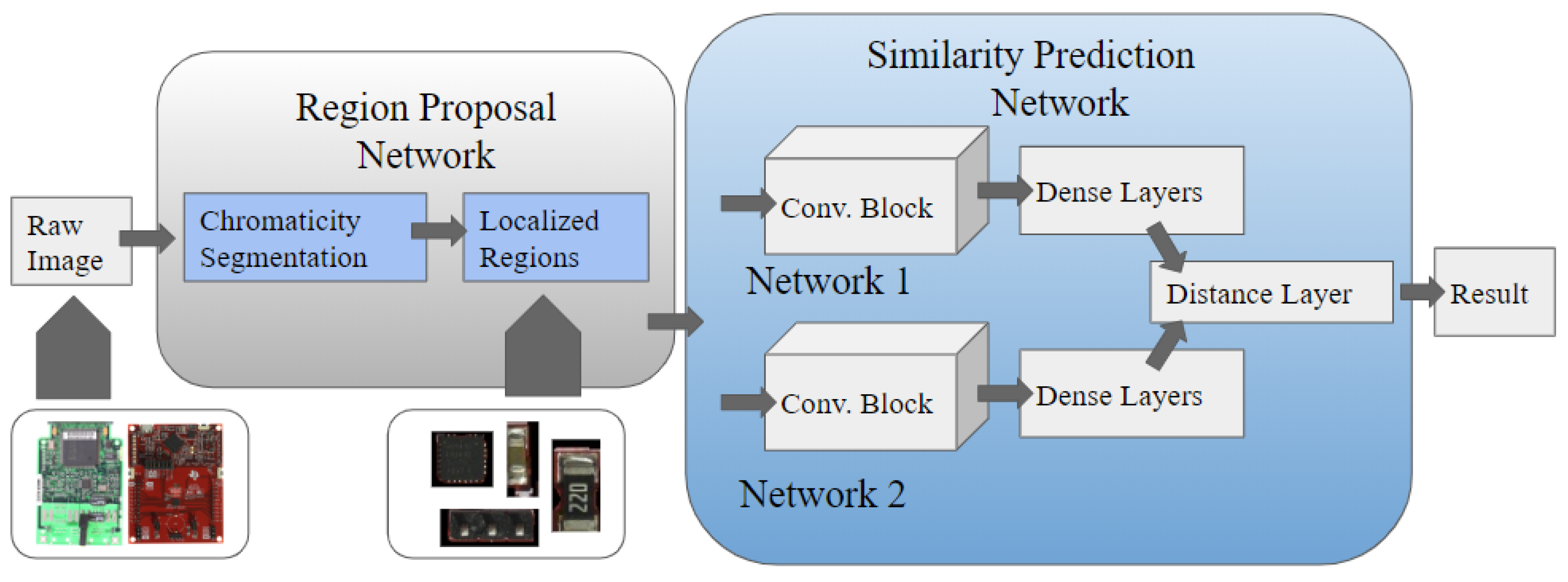
In this section, we propose the electronic component localization and detection network (ECLAD Net), a specialized neural network built for PCB component detection, presented in
Figure 4. ECLAD-Net consists of two stages: region proposal and classification. Each stage is detailed in the following subsections.
4.4.1. Region Proposal Stage
As discussed in
Section 2, the field of PCB assurance has many aspects of high intra-class/low inter-class variance which are unique. Unlike many conventionally-researched applications, which tend to feature natural scenes with a large variety of colors and textures, irregular contours, and sparsely-populated objects of interest, PCBs are more structured. For example, PCBs tend to feature artificial designs with a limited variety of colors, rectangular contours, and a multitude of densely-packed components with varying appearances. Since PCB backgrounds (i.e., the boards) tend to comprise a small distinct range of colors (e.g., green, blue, red), we developed a color-based background subtraction algorithm inspired by chroma-keying.
Though exact details are proprietary information and a patent has been applied for, the general procedure used in this study to achieve color-based background subtraction are as follows. First, various-sized median and gaussian filters were used to reduce noise. Then, the original, unfiltered image and the filtered image were both converted into the Hue Saturation Value(HSV) color space. Since PCB backgrounds are relatively monochromatic and highly reflective, Hue channel thresholding and Saturation/Value reflection detection are used to model the background. The background model is then post-processed using binary morphological operations and used to isolate the individual PCB components in the unfiltered and filtered images. Region proposals are determined by averaging the two results. This is done to maintain both high frequency information (e.g., pins densely-packed resistors and capacitors) and low frequency information (e.g., packaging, ICs). A rectangle detector is then used to refine the region proposals, which may contain ICs, pins, ports, resistors, capacitors, etc. or just background. An example of the output of stage one is shown in
Figure 5 (Left). Regions were then normalized and fed into the next stage of ECLAD Net.
4.4.2. Classifier Stage
In addition to the region proposal stage, we also present a specialized classification stage: a similarity prediction network similar to [
37]. In [
37], two CNNs were trained in parallel and the final layers were merged with a distance metric. This enables the network to learn both discriminative information. In this study, two modified 3 Layer CNN networks (as presented in
Section 4.3.1) were used as the twin CNN architectures. The final layers were merged by applying the distance metric in Equation (
1) below.
where
and
are the transformed input features from each of the twin CNN architectures. To capture the error for iterative learning, a weighted convex sum called contrastive loss [
38] is used at the distance layer to ensure similar images are embedded closer in the feature space. Hence, minimization is done over the distance metric discussed in Equation (
1) using the contrastive loss function in Equation (
2).
where
m, the margin parameter, was set to 1 in this study. As there are two classes in our study, we make use of two twin CNN setups for each class, i.e, two similarity prediction networks. During training, both twin CNNs were fed the same set of images and trained in parallel. However, one of the twin networks is specialized for classifying resistors, while the other is specialized for capacitors. During classification, for each twin network, one CNN is provided a template from the manually cropped dataset (a capacitor or resistor), and the other CNN iterates over the region proposal. Regions that are similar to the template image are then isolated with a match score; thus, for each region proposal we obtained a probability of it being a resistor and another probability of it being a capacitor. The class with the highest classification probability was deemed to be the predicted class. In addition, we performed the same test using three different templates for generalizability; the mean scores were then classified into the two classes. To extend this method to classify additional types of components, additional specialized networks are necessary for each class.
4.5. Evaluation
For the classification experiment, the classifier stage of ECLAD Net (
Section 4.4.2) is compared with the existing classifiers described in
Section 4.2.1. To evaluate the classifiers’ performances, training and testing accuracy are used. A significant performance degradation from training to testing accuracy is indicative of model over-fitting. For the classification experiments, accuracy is a measure of recall given in Equation (
3).
For further insight regarding the class separability of the data, t-SNE [
39] was used. t-SNE is an unsupervised, non-linear feature reduction technique commonly used to visualize high-dimensional data by projecting it onto a low-dimensional manifold. Here, several t-SNE tests were conducted using various parameters; e.g., a perplexity of 10 to 30 and a step size of 10 to 20 were explored.
For the detection experiment, ECLAD Net (
Section 4.4), is compared with the existing detectors described in
Section 4.3.1. To evaluate the detectors’ performances, in addition to recall, precision, given in Equation (
4) is also used.
An additional metric called F1-score is also evaluated. This is a harmonic mean between precision and recall scores and does not incorporate the biases of the individual metrics but rather combines their shortcomings into one, as seen in Equation (
5).
In the field of PCB assurance, a recall degradation indicates that trustworthy hardware is incorrectly flagged as suspicious, while a precision degradation indicates that suspicious hardware is incorrectly deemed trustworthy. Though the former may result in wasted resources (e.g., increased human SME involvement, tossed PCBs), the latter means an unsecured supply chain.
5. Results and Discussion
Results for the classification and detection experiments described in
Section 4 are presented below.
5.1. Classification of Resistors and Capacitors
Table 2 presents the training and testing accuracy of the various classification methods, as described in
Section 4.2. Our findings are detailed in the following paragraphs.
The squared error linear classifier, one-hidden layer dense NN, and VGG16 demonstrated the lowest testing accuracy. The baseline squared error linear classifier performed as expected, as the classifier’s assumption of a Gaussian distribution was not an accurate estimation of the data’s Bernoulli distribution. Results of the one-hidden layer dense NN indicate that the data is too complex for such a small architecture to efficiently understand and model. On the other hand, the significant performance degradation between VGG16’s training and testing accuracy implies over-fitting. This means there is not enough data for such a large architecture to regularize. Though the dataset can be augmented, there still remain limitations in the PCB assurance domain, especially concerning hardware Trojans (
Section 2). These findings suggest that an ideal learning model should be nonlinear, larger than a one-hidden layer NN, and smaller than VGG16 in terms of the number and the size of layers.
The hinge linear classifier, two-hidden layer dense NN, and two-convolution layer CNN, all show accuracy in the 90 to 100 percentage range (
Table 2). Results of the hinge linear classifier indicate that there exists a feature space in which the problem is linearly separable for the most part, but there still exists a few outliers. The two-hidden layer dense NN performed better than the one-hidden layer model, which supports that the latter model was indeed too small for this application. The results of the two-convolution layer CNN emphasize the importance of extracting local shapes and textures for detection and classification. These findings support that local images features are important for PCB component classification, as conceptually discussed in
Section 2.
The three-convolution layer CNN and ECLAD-Net classifier consistently demonstrated the highest performance (
Table 2). The three-convolution layer CNN performed slightly better than the two-convolution layer model, however both require hundreds of examples of each class. In contrast, the ECLAD-Net classifier can learn with as few as single-digit amounts of examples per class. This is ideal for the single-PCB scenario, where an operator or an end-user wishes to authenticate a purchased PCB. While resistors and capacitors are relatively common, there are many other types of components that are uncommon such as crystal oscillators; Zener diodes; and hardware Trojans, which are specifically designed to go undetected. Though 10 images per class is sufficient to obtain excellent results, the ECLAD-Net classifier’s siamese network architecture [
37] is inherently capable of training on a single instance of an image class with decent accuracy.
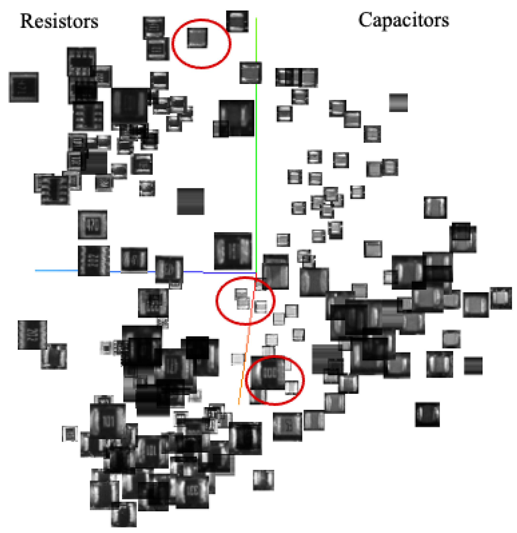
In addition to evaluating the training and testing accuracy for the classification experiments, a 3D t-SNE visualization of the resistor/capacitor separability is also trained and presented (
Figure 6). Samples were collected to represent a wide variety of the possible resistors and capacitors. Though most instances were identified correctly, there were a few failed cases, which will be discussed later in
Section 5.3.
With the classification accuracy and the t-SNE visualization, we establish that resistors and capacitors, and in extension a variety of other PCB components, can be classified. In the next section, we discuss the results of the detection experiments.
5.2. Detection of Resistors and Capacitors
Table 3 presents the precision, recall, and F1 scores of the various detection methods, as described in
Section 4.3. Findings are described in the following paragraphs.
As shown in
Table 3, SSD, modified SSD, and RCNN demonstrated decently high recall scores, but relatively low precision. As discussed in
Section 4.5, a low recall indicates trustworthy components are incorrectly flagged as suspicious, while a precision indicates suspicious components are incorrectly deemed trustworthy, a more dangerous scenario. In other words, though the three methods rarely miss resistors or capacitors, they return numerous false positives. Such results are predominantly due to the number and quality of returned object proposals. Networks such as these are typically designed to locate objects with a high recall, while a threshold must be manually set to filter out false positives. However, as demonstrated, this generic approach is not always sufficient in the PCB assurance field, which exhibits very dense placements of low inter-class/high intra-class variance components (
Section 2).
A notable object proposal complication, apart from missing objects, is the grouping of multiple components. In this study, SSD and RCNN had approximately half the proposed regions included multiple components, thereby complicating the predictions. Therefore, the accuracy of the region proposal system is just as important as the classification system. For example, SSD, which had a VGG backbone larger than the amount of data could support, returned more false region proposals and hence performed worse than the modified SSD, which had a smaller backbone. RCNN, with its selective search, faces similar problems. In one experiment, selective search returned more than 2000 region proposals, with only 75 instances of resistors or capacitors. Even after non-maximal suppression, many false positives still remained present. In the field, these large amounts of false positives, which must be manually-reviewed by human SMEs, are impractical for real-time PCB assurance. In addition to precision and recall, which describe only the effectiveness in a subset of the results, overall effectiveness of the approaches is described by the F1 scores in
Table 3.
ECLAD-Net demonstrated the highest performance across all the evaluation metrics (
Table 3). Its background subtraction technique, which is context-based yet still automatic, provides region proposals with a high accuracy in addition to a close-fitting contour such as the MaskRCNN [
40]. In addition, ECLAD-Net’s region proposal stage inherently prevents overlapped regions, which significantly reduces the number of false positive proposals and removes the necessity for non-maximal suppression. The number of region proposals returned by ECLAD-Net’s first stage are on the magnitude of 100s, compared to SSD’s anchor boxes and RCNN’s selective search, which are on the magnitude of 1000s. ECLAD-Net’s region proposal stage, which has only one parameter - a minimum area to capture, is able to operate at various scales.
In addition to the region proposal network, ECLAD-net’s similarity-based classification network is also specialized to improve performance. This similarity-based network is effective for two reasons: (i) it learns discriminative information despite the low inter-class variance between resistors and capacitors, and (ii) it is capable of learning with few instances per class. In addition, ECLAD-Net can incorporate new information by either directly comparing the new samples with the old or by retraining on the newer samples and then comparing for a match.
5.3. Edge Cases
In this study, numerous challenges for PCB object detection were encountered. Though the proposed ECLAD-Net shows significant performance improvement compared to conventional approaches, completely autonomous PCB assurance is far from perfection. For instance, in the component segmentation stage, only about 90% of the components were captured in an unsupervised manner. Though it is possible to modify the parameters and produce near 100% accurate region proposals, such parameter tuning involves a lot of manual effort. Hence, there is still a need for a more intelligent segmentation algorithm.
Figure 6 shows examples of components that were misclassified in the classification experiments. As shown, the similar color and texture patterns make it difficult even for a human operator to identify. Some instances lie so close to the class separation boundary, they slightly overlap into the other region. Though the classification accuracies are above 99%, the field of PCB assurance demands near 100% accuracy (
Section 1). Therefore, future research should focus on these challenges.
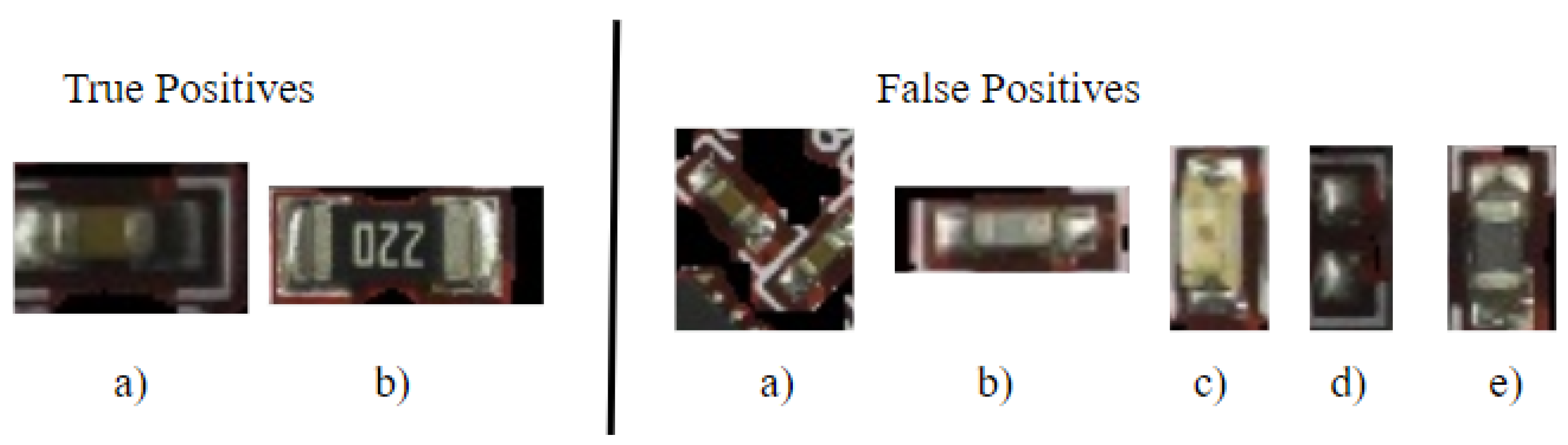
On the other hand, detection leaves a lot more room for improvement. Examples of edge cases are presented in
Figure 7 and described in detail in the following sentences.
For the true positives, we see (a) a capacitor under non-ideal illumination due to being in the shadow of a large component, and (b) a large flat resistor with text in a dataset where the majority of resistors are small and without text. Despite these challenges, ECLAD-Net was still able to correctly recognize them. For the false positives, we see several examples. In
Figure 7a, a horizontally-oriented capacitor is in the same region proposal as another. Here, ECLAD-Net correctly classified them as a capacitor, but failed to identify the two instances as separate.
Figure 7b shows an uncommonly gray capacitor that was misclassified as a resistor. In
Figure 7c, a light brown LED was misclassified as a capacitor due to its similarities to typical SMD capacitors.
Figure 7d shows two solder pads under a shadow that were misclassified as a resistor. Though there is no component here, the shadow creates a false impression of a resistor. In
Figure 7e, a dark gray inductor was misclassified as a resistor. For false positive cases, (c), (d), and (e), recognition can be difficult for even non-experts. Hence, as shown in
Figure 7, there are several edge cases between resistors and capacitors, along with other types of components that were not trained on.
ECLAD-Net has shown to be effective in scenarios popular object detection networks fail, however the above edge-cases show that there is room for improvement by incorporating and learning multiple classes of components. Our current efforts in collecting and building a larger, more comprehensive and representative dataset will help this process and guide future research.
PCB authentication and assurance is another example of dense object detection for which there has been very limited research. It needs specialized approaches and increased attention from the computer vision community. An example of a similar problem is presented in spacenet [
41] which works with dense satellite images; its objective is mainly to detect houses from satellite images, which makes it ultimately, a “one class” problem. Supermarket product detection [
42], on the other hand, deals with multiple classes, but the accuracy of the predictions is not of high priority, yet identifying multiple classes is important. PCB component detection, however, needs accurate localization and classification of various microelectronic components, all of which share a high amount of variance in them. Thus, ECLAD-Net can be utilized for both of these purposes with slight modifications, as they are special cases of PCB component detection. Similarly, this is also applicable to problems in the science and medical spheres for the detection of small components in medical imaging, such as in [
43].
6. Conclusions
In this paper, we proposed and described a network for PCB component detection to identify malicious, counterfeit, reused, or recycled components. We also presented a discussion of the unique challenges in PCB assurance, such as low inter-class/high intra-class variance, dense object placement, and limited data. Popular generic approaches for object detection, such as RCNN and SSD, do not provide the near-perfect performances desired in PCB assurance applications. Therefore, we present a more specialized network called the electronic component localization and detection network (ECLAD-Net). Results from various experiments were presented to compare the proposed ECLAD-Net with existing methods to showcase the need for such specialized networks.
Though ECLAD-net has demonstrated excellent classification and detection performance relative to the generic methods, there is still much room for improvement. While this paper focused on resistors and capacitors, similar problems arise with other components as well, such as ICs and transistors (
Figure 2). Due to the uniqueness and importance of the PCB assurance field, attention and collaboration is necessary from both the hardware assurance community and the computer vision community. While this paper presents some fundamental research to help pave the way, there exists a larger scope for research and improvement, and we hope to continue research in this front.
In the future, we hope to improve our network to provide better precision and recall, while also improving algorithm speed. Component detection is only one part of PCB assurance. Text recognition for serial number verification, texture analysis for counterfeit detection, and 3D analysis for Trojan detection are just a few examples of other areas that would benefit from better and more efficient computer vision algorithms tailored toward PCB assurance and hardware security. In addition, there is also a great need for a larger and more comprehensive dataset for PCB assurance, as the lack of data is currently a bottleneck in applying DL to hardware assurance. To aid the community and help future research, we are in the process of building a public dataset and currently have around ten thousand component images.


