
A Novel Ultra-Compact FPGA PUF: The DD-PUF


1
Dipartimento di Ingegneria dell’Informazione Elettronica e Telecomunicazioni (DIET), Sapienza Università di Roma, 00184 Rome, Italy
2
ICTEAM/ELEN Crypto Group, Université Catholique de Louvain, 1348 Louvain-la-Neuve, Belgium
*
Author to whom correspondence should be addressed.
Cryptography 2021, 5(3), 23; https://0-doi-org.brum.beds.ac.uk/10.3390/cryptography5030023
Submission received: 16 July 2021
/
Revised: 29 August 2021
/
Accepted: 2 September 2021
/
Published: 8 September 2021
(This article belongs to the Special Issue Implementation and Verification of Secure Hardware against Physical Attacks)
Abstract
:In this paper, we present a novel ultra-compact Physical Unclonable Function (PUF) architecture and its FPGA implementation. The proposed Delay Difference PUF (DD-PUF) is the most dense FPGA-compatible PUF ever reported in the literature, allowing the implementation of two PUF bits in a single slice and provides very good values for all the most important figures of merit. The architecture of the proposed PUF exploits the delay difference between two nominally identical signal paths and the metastability features of D-Latches with an asynchronous reset input. The DD-PUF has been implemented on both Xilinx Spartan-6 and Artix-7 devices and the resulting design flows which allow to accurately balance the nominal delay of the different signal paths is outlined. The circuits have been extensively tested under temperature and supply voltage variations and the results of our evaluations on both FPGA families have shown that the proposed architecture and implementation are able to fit in just 32 Configurable Logic Blocks (CLBs) without sacrificing steadiness, uniqueness and uniformity, thus outperforming most of the previously published FPGA-compatible PUFs.
1. Introduction
The usage of dependable devices such as smartphones, PCs, tablets, smart-cards and digital tokens is nowadays omniscient. Government, banking and social networks data are constantly stored in databases. Over the years, several cryptographic methods have been proposed to ensure the user’s data privacy. All modern cryptographic algorithms need cryptographic keys to protect the user’s data. In the last two decades several tampering techniques (e.g., micro-probing, focused ion beam, glitch attacks and side-channel attacks) have proved to be the weakness of stored keys approach in cryptographic hardware devices.
In the last decade, Physical Unclonable Functions (PUFs) have played an important role as hardware’s protection mechanism for generation of identification strings and cryptographic keys [1]. A PUF is a physical entity that produces at least one hard to clone output that is a function of the device’s physical implementation [2]. By exploiting process variations and mismatch, PUFs can generate a “fingerprint” that can be used as cryptographic key or unique identifier for (physical instance of) a device [3]. Compared to classical key-storage methods, such as Non-Volatile Memories (NVMs) and EEPROMs, keys generated by PUFs are not stored physically on the device, being generated identical to themselves at each new usage. Furthermore, reverse-engineering of PUF-based devices can be not trivial due to unpredictability of manufacturing process variations. This particular feature has given birth to new PUF-related security applications, such as intellectual property protection, cloning/counterfeiting prevention and complex security-on-chip design [4,5,6,7,8]. Implementing on-chip PUFs allows to considerably cut down the overall cost of secure devices while providing a baseline solution for a hardware root-of-trust (RoT) [9]. Clearly, PUFs can be deployed on ASICs, leveraging on analog and/or digital circuitry, or, at a lower cost, on Field Programmable Gate Arrays (FPGAs).
FPGAs are widely diffused in embedded systems as well as on high-end systems due to their re-configurable nature, performance, efficiency and cost. However, hardware resources in FPGAs are limited and the integration of security modules can be challenging. Moreover, due to the lack of routing resources and dedicated building blocks, FPGA-based solutions are more and more constrained than their ASICs counterpart. In the context of PUFs, the entropy that could be extracted from FPGA-based architectures is critically dependent on the placing and the routing compared to ASIC implementations [10].
Considering the usage of PUF keys in cryptographic protocols, it is necessary that at each new usage the PUF fingerprint remains unaltered, even under temperature and supply voltage variations. Unfortunately, reliability of PUFs is sensitive to design parameters (e.g., unwanted mismatch in symmetric architectures) as well as environmental conditions (e.g., temperature and voltage variations) and, therefore, a good PUF deployment requires careful design and floor planning.
Among most common PUF architectures, the SRAM PUF, introduced independently by Guajardo et al. [11] and Holcomb et al. [12] is one of the most popular. It is based on the unpredictability of SRAM cells’ output at power up. The initial state of SRAM cells on FPGAs is usually very predictable, making this approach not suitable to design a good PUF. Butterfly PUFs [13] exploit the metastability of a pair of cross-coupled latches, making it suitable also for FPGA implementations. The sampling of the oscillation frequency of different ring-oscillators has been exploited to design Ring-Oscillator PUFs (RO-PUF) [7]. RO-PUFs are suitable to be implemented on ASICs as well as on FPGAs due to their simplicity, but they have been found particularly sensitive and vulnerable to electromagnetic attacks [14]. In addition, this PUF architecture is affected by the locking phenomenon which dramatically reduces the reliability of the circuit. To solve this issue, Bousset et al. have proposed the Transient Effect Ring Oscillator PUF (TERO-PUF) [15], which is based on the oscillatory metastability of a TERO cell. Lately, Arbiter PUFs [16] and Interpose PUFs [17] have become particularly popular for being FPGA-friendly and easy to integrate. They exploit process-dependent differences of two (or more) delay lines to attain unique identifiers. In [18], Gu and O’Neill have proposed a compact PUF suitable for FPGA implementation based on the arbiter architecture, which was later renamed Pico-PUF [10].
In this work, we present a novel FPGA-compatible and ultra-compact PUF, which requires a very small area footprint and provides very good reproducibility under temperature and supply voltage variations. The proposed PUF, namely the Delay Difference PUF (DD-PUF), has been implemented on a Xilinx Spartan-6 LX16 (45 nm technology) and Xilinx Artix-7 100T (28nm technology), and has been tested in a wide range of temperature and supply voltage variations. To the best of our knowledge, the proposed design is the most compact FPGA-compatible PUF ever reported in the literature, offering a density of 2 bits/slice.
The structure of the paper is described as follows. In Section 2, we summarize the state of the art of PUF designs suitable for FPGA implementation. The metrics used in the context of PUFs evaluation are reported in Section 3. In Section 4, we introduce the architecture and the FPGA implementation of the proposed DD-PUF, outlining the design approach for Spartan-6 and Artix-7 families. Experimental validation and results are shown in Section 5. A comparison with the state of the art is presented in Section 6, and finally conclusions are drawn in Section 7.
2. Related Works
In this section, we briefly recall the most important PUF architectures which are suitable to be implemented on FPGA platforms.
2.1. Butterfly PUF
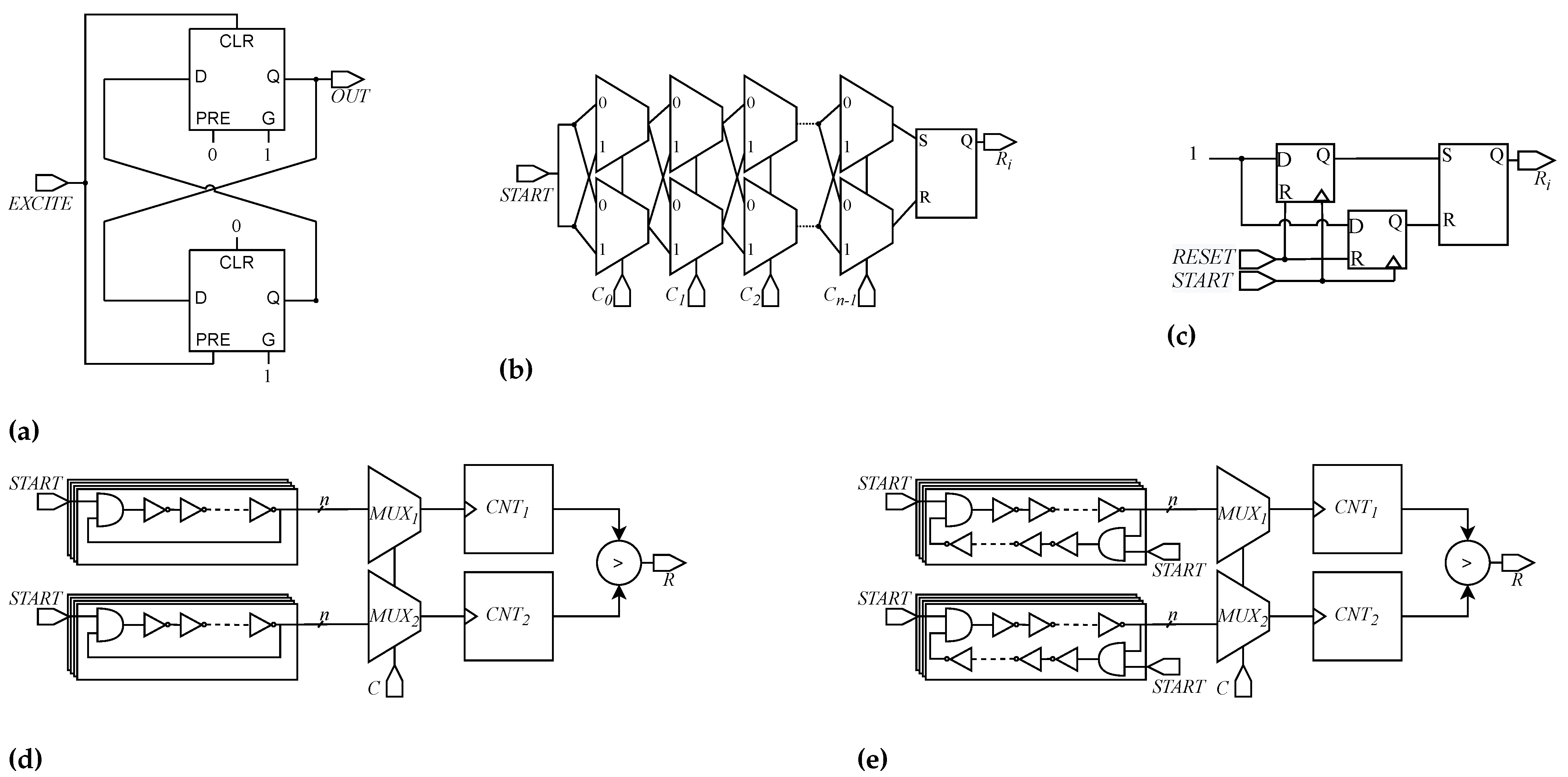
Kumar et al. have proposed in [13] a weak-PUF realization called "Butterfly PUF" (BPUF), which is based on a cross-coupled pair of latches. The main idea is to excite this cross-coupled pair in order to force a race condition between the two latches. A single control signal, namely , is used to produce the output bit, as shown in Figure 1a. This signal is connected to the clear pin on the upper latch and to the pre-charge pin on the lower one (it is assumed that and are both active high), while both latches are permanently transparent. The generation of the unique bit is structured in three phases. During the first one, the control signal is set to 0 and therefore the OUT signal stays at its initialization value (0 or 1 depending on the designer choices). Next, the signal is forced to 1 for a certain time interval, making the cross-coupled pair unstable, as the both latches see opposite signals on their input and output. When is forced to 0, the output bit of the BPUF is produced, depending on the process-dependent random differences between the two branches. The implementation of the BPUF relies on the possibility to control separately the pre-charge and clear of the two latches along with the possibility to obtain a symmetric and balanced routing between them. This aspect can limit its applicability and performance to some platforms. For example, latches within the same slice in Xilinx FPGAs share the same control signals. Thus, a BPUF on such platforms would require to use latches from different slices, impacting on the possibility to obtain a symmetric structure and limiting the performance of the circuit.
2.2. Arbiter PUF
Lim et al. have proposed a PUF called Arbiter PUF (APUF) [16]. The APUF, depicted in Figure 1b, exploits random variations on the propagation delay of two symmetric branches. The same signal is fed to both signal paths, and a set of multiplexers, controlled by challenge bits, routes the two wires towards an SR-latch, used as a simple arbiter. To assure that the output response depends only on process and mismatch variations, the routing of the APUF cell should be performed manually. Due to its simple structure and rationale, the APUF is nowadays one of the most common and widely used PUF. Moreover, several strong PUF designs exploit the APUF as front-end entropic-source. Nevertheless, this PUF is resource demanding as the number of logic cells (i.e., slices) per bit can be quite high.
2.3. Pico-PUF
Gu et al. have proposed a compact and robust arbiter-based PUF, in which each bit requires two LUTs, two flip-flops, used as toggle (T-type) flip-flops and an additional multiplexer [18,19]. In later works from the same authors [10,20], this architecture has been re-arranged to save two LUTs, and D-type flip-flops have been used instead of T-type ones. The resulting Pico-PUF, shown in Figure 1c, takes advantage of random variations on the propagation delay of two symmetric branches involving the flip-flops, and extracts this difference by using an arbiter cell, implemented as a NAND SR-latch. A challenge bit drives a multiplexer to select one of the arbiter’s complementary output as PUF’s generated bit. The Pico-PUF is controlled by and signals. First of all, forces both Q signals of flip-flops to 0. After this initialization phase, is set to 1, triggering the run between the two symmetrical branches. The SR-latch arbiter will set its outputs according to which of the aforementioned flip-flops’ output reaches 1 first. It has to be noted that the reliability of the Pico-PUF strongly depends on selected sites, as noted in [20]. Therefore, the authors have proposed a semi-automated placement technique that has to be performed per device to mitigate reliability issues in Pico-PUF arrays.
2.4. Ring-Oscillator PUF
In 2007, Suh et al. have proposed the Ring-Oscillator PUF (RO-PUF) [7]. The RO-PUF is one of the most common FPGA-compatible PUF [21], due to the simplicity of its design, high reliability and reproducibility. The topology, depicted in Figure 1d, exploits N oscillators, each of which harness an M number (where M is an odd integer) of inverters. A single PUF response bit is generated by comparing the oscillation frequency of two oscillators, estimated by two counters. To generate a 128-bit PUF response, it is necessary to consider the amount of entropy generated by ring-oscillators pair-wise. Clearly, N oscillators generate a maximum entropy of , and the quality of the response may be reduced by the correlation between oscillators’ frequencies. An alternative way to mitigate this problem and improve the entropy is to use ring oscillators, each paired with a reference one, generating an N bit response for a given N bit challenge. Compared to other delay-based PUFs, the response read-out is slower since it requires k clock cycles (eventually, the measuring time window) to generate one PUF response bit and therefore cycles to generate an N-bit PUF response. It is clear that the RO-PUF requires a huge amount of resources, and therefore cannot be considered a compact solution for constrained applications. In addition, RO-PUFs are extremely vulnerable to side-channel-assisted modeling [14], which are able to undermine the unpredictability of the RO-PUF responses.
2.5. Transient Effect Ring Oscillator PUF
Bousset et al. have proposed the Transient Effect Ring Oscillator PUF (TERO PUF) [15], later characterized in [21], as a variant of RO-PUFs. Each ring in a TERO cell is composed of a certain number of inverting stages. Compared to classical RO-PUFs, the TERO-PUF provides two possible states: a transient oscillating state and a stable state. Each TERO cell is a metastable structure consisting of two symmetrical and nominally identical branches, each of which is composed of an odd number of inverters and two AND gates (resembling the structure of a NAND SR-latch, with set and reset inputs tied together). Setting the signal to 1, the TERO cell is forced to be in an unstable state, and oscillation events are triggered on both branches. Depending on the delay mismatch between the two branches, these two events would collide and the TERO cell stops oscillating, entering in a stable state condition. The response of the TERO-PUF is extracted by selecting and accumulating some of the bits given by the comparison of the number of oscillations generated by two TERO cells excited with a selected set of challenges. Furthermore, the TERO-PUF is usually a resource demanding architecture which requires a post-elaboration phase in order to attain minimum performance in terms of steadiness and reliability. Similarly to the RO-PUF, cycles are required to generate an N-bit response [22].
3. Background
The most used metrics to quantify PUF performance are Randomness, Uniqueness and Reliability. Since each PUF (physical) instance has to generate the same random response under different environmental conditions, it has to be rigorously characterized under process, temperature and supply voltage (PVT) variations.
3.1. Randomness
In cryptography, the quality of random numbers plays a key role, and therefore their properties require a thorough assessment. It has to be noted that each PUF generates an n-bit response depending on a certain challenge string, and to ensure its unpredictability it is needed to investigate its randomicity [23]. The place and route of the PUF, and more in general its floor planning, is a key step in the design of a PUF. As a matter of fact, a bad floor planning could impact negatively on the quality of a response, and deterministic features, such as unbalance and periodicity, could affect the response. This phenomenon can arise in Arbiter PUFs as reported by [20], and an extra effort has to be spent to mask the bit-cells that present unwanted features.
A subset of the NIST random test suite [24] can be adopted with the aim of investigating the randomness performance of the whole generated PUF response. In fact, even if this test suite refers to Random Number Generators (RNGs), it can be adapted to characterize PUFs as well. According to previous works [21,25,26,27,28], the following subset of NIST tests can be exploited to properly evaluate the randomness of PUFs response:
- Mono-bit frequency test: aims to characterize the 1/0 bias of the response to a given challenge;
- Block frequency test: along with mono-bit frequency test, it checks the group bias of the PUF’s response;
- Cumulative sum test: it aims to study the number of 1s in the progressive partial sums of input sequence (the response in this context);
- Run test: it estimates the sequence of consecutive 1s and 0s in sub-string sets, evaluating if the number of oscillation between homogeneous strings is too fast or too slow;
- Longest run test: its purpose is to find the longest sequence of ones in n-bit strings subdivided in N sub-strings of M bits;
- Approximate entropy test: it scans M-bit sequences of a given response in order to find identical adjacent ones.
Each of the above tests produces a non-negative rational value called the p-value. The p-value is the probability that a perfect RNG would have generated a sequence that is less random that the one under test [24]. Moreover, some of the tests require changes from default settings (e.g., the block frequency test), as recommended by the official document from NIST [24]. The PUF fingerprint passes the given test if the p-value is greater than 0.01 [21].
3.2. Uniqueness
This comparison metric quantifies the differences between the responses of several implementations of the same PUF on different devices (FPGAs or chips). In other words, Uniqueness evaluates process variations and mismatch effects on PUF outputs. In order to study the uniqueness of a PUF, the same design should be physically implemented on different devices. Furthermore, each of these devices should be excited with the same stimuli (and challenges) as well as the same environmental conditions. Therefore this metric is computed as the average value of the sum of inter-class Hamming Distance (HD) between each possible pair-wise response couple. Hence, considering k realizations of the same PUF circuit, the inter-class HD in percentage is defined as [2]:
where an n-bit response for the i-th instance () has been taken into account and both process and mismatch variations have been considered. Since each PUF fingerprint should be unpredictable, the same challenge applied to n PUFs should produce different responses. As a result, the ideal n-chip inter-class HD should be 50%.
3.3. Reliability
It quantifies how much the PUF can reproduce the same response to a given challenge in different sessions and/or in different working conditions. To evaluate this metric, a PUF challenge-response is chosen as a reference and compared with fresh ones generated with the same challenges and stimuli. At each measurement the PUF should be re-initialized. The Reliability is particularly relevant in authentication systems based on Challenge-Response Pairs (CRPs), as it is necessary to guarantee the steadiness of the PUF response to a given challenge [2]. The Reliability analysis is performed by computing the intra-class HD between the Golden-Key (GK) response collected in nominal condition, and k fresh responses, clustered according to their respective power supply voltage and working temperature (typically of the nominal and T ∈ [0 °C, 75 °C]). This approach allows to provide a full PUF characterization, covering a broad spectrum of possible working conditions. In detail, the Reliability is defined as follows [2]:
where represents the generated i-th response at a given power supply voltage and temperature, and the reference GK one.
Many applications of PUFs may require some additional error-correction mechanisms to ensure a minimum steadiness of the response. Error-Correcting Codes (ECCs), such as BCH or Reed-Solomon, are adopted to compensate the effect of voltage and temperature variations on the response of PUFs, as well as defective behaviour of some bits (that can occur also in nominal conditions) [2,3]. Clearly, the adoption of such correcting mechanisms requires additional resources, hence, increasing the footprint of the overall PUF primitive.
4. DD-PUF Architecture and Design
In this work, we propose a novel FPGA-compatible and ultra-compact PUF, which leverages on the delay difference between two nominally identical signal paths and on metastability features of memory elements, delivering a new PUF solution with high-reliability and stability under PVT variations. The rationale behind the proposed Delay Difference PUF (DD-PUF) is to optimize the resources required by a single bit-cell, focusing on FPGAs’ intrinsic architecture without compromising the overall performance. In this section, the architecture and the FPGA implementation of the DD-PUF are discussed.
4.1. Architecture
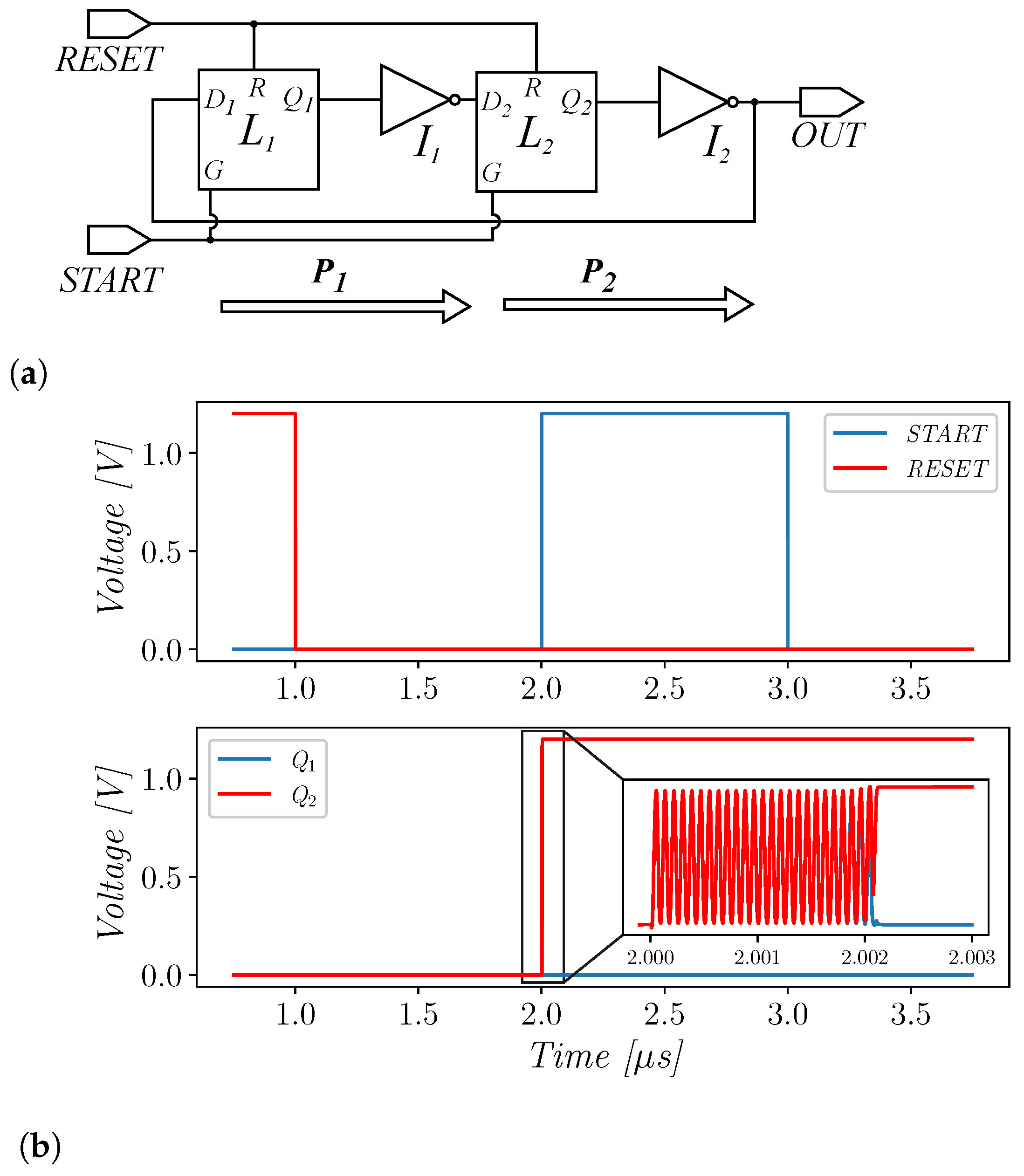
The architecture of a single DD-PUF cell is depicted in Figure 2a. The bit-cell is composed of two inverters, namely and , interposed between two D-Latches (DLs), namely and . Two paths can be identified in a DD-PUF cell: from the D input of / to the output of inverter /, denoted as and . The DD-PUF needs two control signals, and (both at 0 when the PUF is in idle), connected to the enabling gate and clear pin of the two latches, respectively. When the asynchronous is set to 1, both latches’ output pins are forced to 0.
The sequence of operations to correctly stimulate a DD-PUF cell is divided in three phases:
- Initialization phase;
- Evaluation phase;
- Output phase.
During the initialization phase, the signal is raised from 0 to 1 while is kept low. Hence, outputs of the DLs are forced and initialized to 0 while their inputs are consequently forced to 1, due to the presence of and . When the signal is set back to 0, the PUF is left to settle. After a rest time, the signal is set to 1 for a time interval , that corresponds to the evaluation phase. During the evaluation phase, the DLs become transparent, and an oscillatory state is produced within the DD-PUF cell. At this point, only the small delay difference between the two (nominally) identical paths determines the resulting stable bit, hence the name "delay difference" of the proposed architecture. The working principle of the DD-PUF cell has been investigated and validated through Cadence Virtuoso, using a commercial 65nm design kit. A full stimulation sequence of a DD-PUF cell is depicted in Figure 2b. By observing the internal nodes of the cell it is clear that when START signal is raised, oscillatory metastable events are triggered. The oscillatory state ends within a certain time, after which a steady and stable state is reached. The amount of time needed to reach a stable output is related to the delay of routed connections, the intrinsic inverter propagation delay, and delay of the two latches [29]. When the stable state is reached, signals are complementary and START can be set back to 0, therefore the response is available for the readout.
For the sake of clarity, a simple model of the response bit generation is given as follows. Consider individually the total delay of the two aforementioned paths and , assuming that are identical to each other for simplicity. Concretely, and have also an impact, as they contribute to the total delay of path when the evaluation phase starts, adding another process-dependent source of entropy to our PUF:
where is the delay of the i-th DL, and is the propagation delay of the i-th inverter. Therefore, the delay difference between and is:
As we have stated before, a DD-PUF cell digitizes this delay difference considering the sign of ; hence, the output bit can be expressed as:
In order to fully exploit manufacturing variations and improving the unpredictability, the proposed PUF cell requires that the two paths are nominally routed with the same delay. It is straightforward to notice that when the signal is set back to 0, the two latches cannot change their output data and the internal state of the PUF is hold. We remark that if the cell does not reach a stable state in a time interval shorter than , the latches may capture metastable states that are not advisable to be used in this context, as they may impact negatively on the steadiness of the response.
4.2. FPGA Implementation
The proposed DD-PUF architecture has been implemented in both Xilinx Spartan-6 and Xilinx Artix-7 devices. The design is easily portable also to the whole Series-7 from Xilinx, as they all share very similar Combinational Logic Blocks (CLBs) and slice architectures, showing the portability and feasibility of the proposed topology on different platforms. The design has been carried out adopting Xilinx ISE 14.7 when targeting Spartan-6 devices and Xilinx Vivado 2020.1 when targeting Artix-7 FPGAs. As was clarified in Section 4.1, the design of a DD-PUF cell requires some special considerations. In particular, the physical implementation of the DD-PUF cell has been conceived for minimizing resource usage, while ensuring an almost perfect matching of the two paths and in terms of delay. The first important result that has to be pointed out is that all the four elements needed to implement the proposed DD-PUF cell in Figure 2a can be placed on half of a slice, independently of the architecture of the slice itself (X/L/M for series-6 and L/M for series-7 [30]). In fact, each slice in a Xilinx FPGA provides eight configurable registers, four of which can be used as latches. Referring to these components, it is crucial to notice that the control signals (clock/gate, clear/reset, enable) of registers and latches in a slice are shared. Furthermore, a slice provides four single-output 6-input LUTs, each of them can be also configured as dual-output 5-input LUTs [30]. As a consequence, the DD-PUF cell can be implemented using just two LUTs and two latches within a slice. An additional output multiplexer can be easily implemented exploiting unused LUTs’ outputs or adopting in-slice multiplexer resources, namely MUX-F7/8. It has to be noted that in Xilinx Spartan-6, the MUX-F7/8 are available just in type-L and type-M slices. The selected design exploits one of the LUT 2:1 output to provide the multiplexed bit and decouple parasitic effects. Summarizing all the above considerations we can remark that the proposed architecture is quite dense, requiring only 0.5 slice/bit. Compared to the state of the art, a DD-PUF cell requires the smallest amount of resources, reducing the footprint required by 50% with same technology as the Pico-PUF, which is the most compact PUF in the literature. Another important feature achieved by the proposed PUF is that the bit-cell does not need any particular placement restriction in terms of CLB or slice.
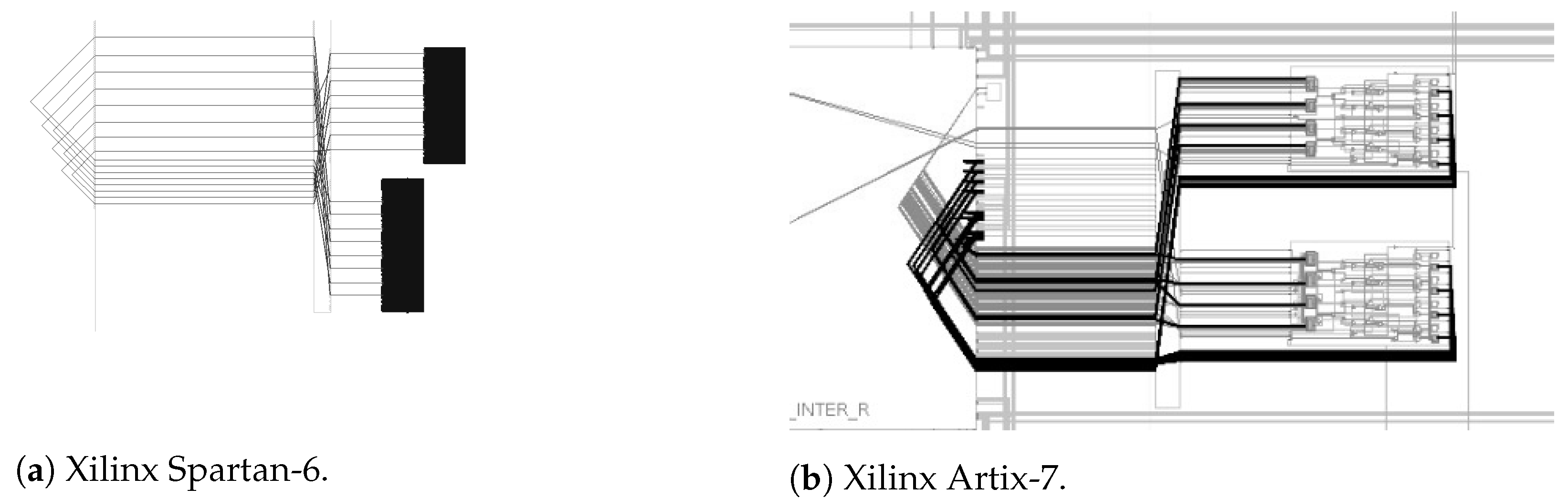
As we have discussed above, the DD-PUF requires matching of (nominal) delay paths and to fully exploit process-dependent differences and enhance the bit-entropy. Hence, we have explored all possible routing paths that each switch matrix for each type of slice offers. We have observed some minimal but critical differences in switch matrices belonging to difference type slices in the Artix-7 FPGA. To further improve the matching of and , we limited the routing possibilities to paths inside the switch matrix that allow a direct connection between output and input pins of a slice, selecting delay-matched paths only. Floorplans of four DD-PUF cells for the Xilinx Spartan-6 and Xilinx Artix-7 FPGAs are depicted in Figure 3a,b, respectively. This step has required a thorough investigation of all possible output/input routing paths of each type of slice, as the manufacturer does not provide any resource concerning this aspect. Jointly, also the configuration of the LUTs and their pin configuration has requested a in-depth investigation, in order to deploy a good matching. It is worth noting that the routing between the LUTs/inverters and their respective DLs is intra-slice, ensuring maximum exploitability of manufacturing-dependent variations. A summary of nominal delay differences on critical nets of a 2-bit DD-PUF macro (that is, implemented on a single slice) is reported in Table 1. We have performed the static timing analysis on critical nets of 2-bit DD-PUF macro for both platforms, and delay differences are reported in Table 1. Differences of branches’ delays in Table 1 confirm the extreme balancing of the routing achieved on both FPGA families.
It has to be noted that the differential structure of a DD-PUF cell offers some advantages also from a side-channel perspective. All signals in a DD-PUF cell are differential and locally matched, and therefore they do not provide any useful information to a side-channel adversary that is able to monitor power consumption and/or electromagnetic (EM) emission, as the output response is generated leveraging on the steady state. Dynamic phenomena during the oscillatory phase of the DD-PUF are hardly exploitable and their frequency contents is in the order of GHz (see Figure 2b). For an EM adversary, measuring such high frequency can be extremely challenging as well as expensive. Considering a power analysis adversary, such high frequency signal is easily filtered off by power grid’s capacitance (see [31] for similar considerations). Therefore, we expect that side-channel analysis does not represent a strong threat for our proposed architecture, but we will investigate more this aspect to support this claim in future research.
4.3. Discussion
It is important to remark the main differences between the proposed DD-PUF and other similar architectures, such as the BPUF and TERO-PUF cells. In a BPUF, the metastability of latches is exploited, and the generated bit depends on the small difference between the two memory elements. Nevertheless, due to its working principle, the latches that form a BPUF cell are controlled differently with respect to the DD-PUF, as their pre-charge and clear pins have to be independent. As a consequence, a physical implementation of BPUF cells on some FPGAs can be difficult or not optimal (from a delay balancing perspective), as usually those control pins of memory elements are shared among clustered units (e.g., slices in Xilinx FPGAs), requiring extra effort for the design and impacting negatively on the reliability and reproducibility of the PUF itself.
In TERO-PUFs, the bit is extracted out of the number of oscillations of each TERO cell. Therefore, a TERO cell would usually need longer branches, hence more delay stages, in order to guarantee a sufficient number of oscillations before reaching a steady state, and additional circuitry for frequency estimation and bit-extraction. Furthermore, as stated in [21], the attained response is collected from N multiple frequency differences and thus N acquisition windows. This behaviour significantly degrades the TERO-PUF throughput. Our proposed PUF architecture’s response is instead obtained leveraging on the steady state reached by DD-PUF cells after the oscillatory phase. Thus, no additional logic is needed for frequency estimation.
5. Experimental Results
In this section, we report experimental results on the evaluation of the proposed DD-PUF. As a case study, we have considered a 128-bit DD-PUF cell array, meaning that 64 2-bit macros have been placed in a 8 × 8 array. Adopting a macro-based design allowed us to preserve the balanced internal routing and structure of DD-PUF cells, in accordance with Figure 3. The analysis of the DD-PUF has been performed considering a broad range of experimental aspects, in order to fully cover the PVT behavior of the novel FPGA-compatible PUF.
5.1. Setup
Our evaluation campaign has involved 16 boards, mounting Xilinx Spartan-6 FPGAs, and 16 boards mounting Xilinx Artix-7 FPGAs. FPGAs’ core voltage has been supplied by means of Teledyne T3PS43203P programmable power supply unit. We have considered a supply voltage range of around the nominal one, which is 1.2 V and 1.0 V for the Spartan-6 and Artix-7, respectively. The working temperature of the FPGA has been accurately set by using an Espec SH-621 climate chamber, in the range [0 °C, 75 °C], with step of 25 °C. For both type of specimens, a system clock of 50 MHz has been used. We refer hereon to the duration of the evaluation phase in number of clock cycles, considering the system clock period as timing reference.
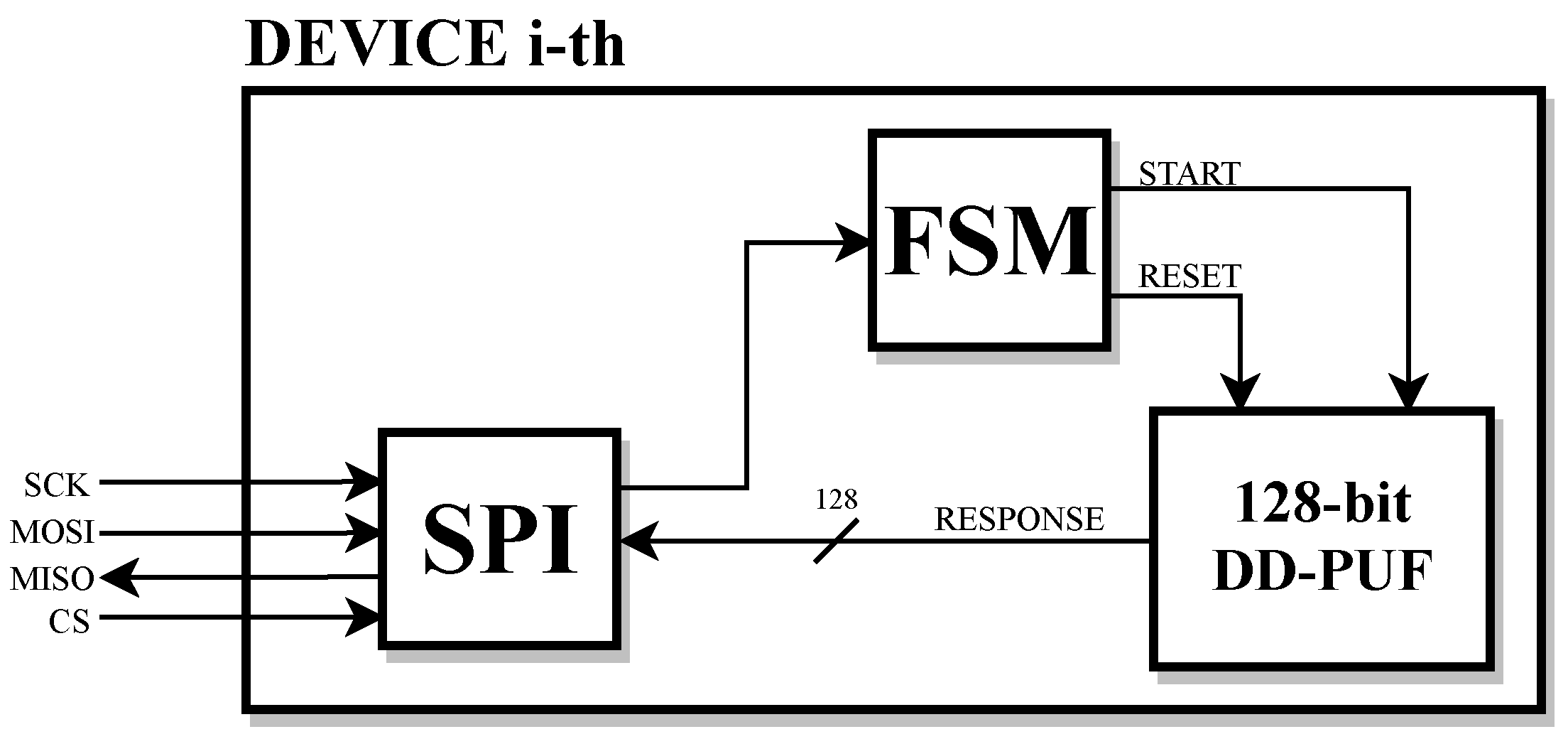
All boards are supervised through a daughter board mounting a FT232H chip, which serves as USB-SPI interface, stimulated by custom Python scripts. The duration of the evaluation phase of the DD-PUF array can be changed through the SPI. By means of this simple but effective testbed, we have been able to evaluate the steadiness of the proposed PUF under different stimuli conditions, revealing some interesting features when power supply voltage variations take hold. The block scheme of the adopted testbed is depicted in Figure 4.
5.2. Reliability and Bias Results
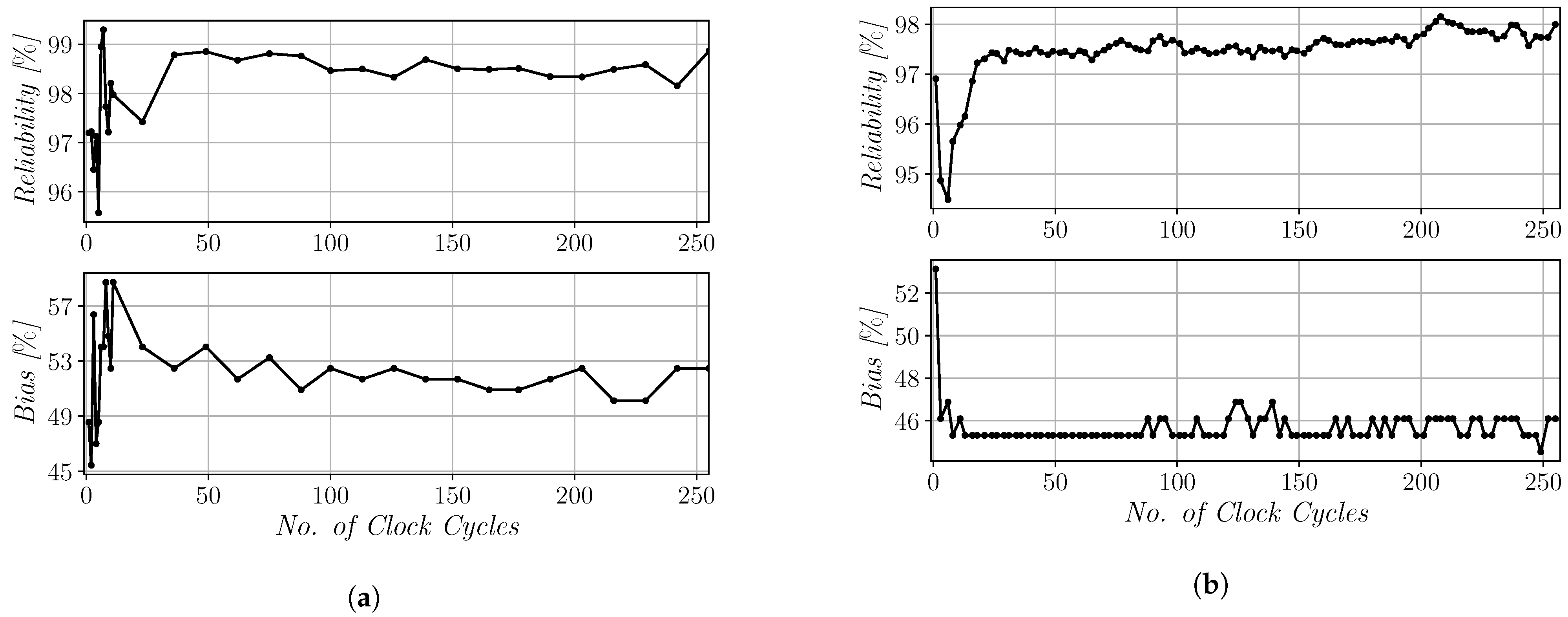
In order to evaluate the reliability we have extracted a GK by averaging 50 × 10 repeated read-out measurements in nominal environmental condition (i.e., and T = 27 °C), varying up to 256 clock cycles for both FPGAs. We have then investigated the reliability and the 1/0 bias of the response as a function of the duration of in nominal conditions, and results are shown in Figure 5 for both FPGA families. This analysis aimed to evaluate the influence of the evaluation phase duration on PUF reliability and bias performance. As it is clear from Figure 5, longer values lead to higher reliability. Measurements results have shown that values of higher than ∼20 clock cycles ensure a reliability higher than 97% for both FPGA families. Considering the upper limits of the evaluation phase ranges, the reliability increases to about 98.37% and 98.33% for the Spartan-6 and Artix-7, respectively. A similar behaviour can be observed regarding the 1/0 bias for both specimens. It is straightforward to notice that a short evaluation phase would not lead to a stable response of the proposed PUF, as both reliability and bias do not provide stable values. This outcome is expected as we need to achieve a stable state in each DD-PUF cell to extract stable bits, and suggests a trade-off between reliability and read-out time. Furthermore, both FPGA families exhibit a similar trend regarding these metrics, remarking that the proposed design can easily be ported across different technologies without degradation of performance.
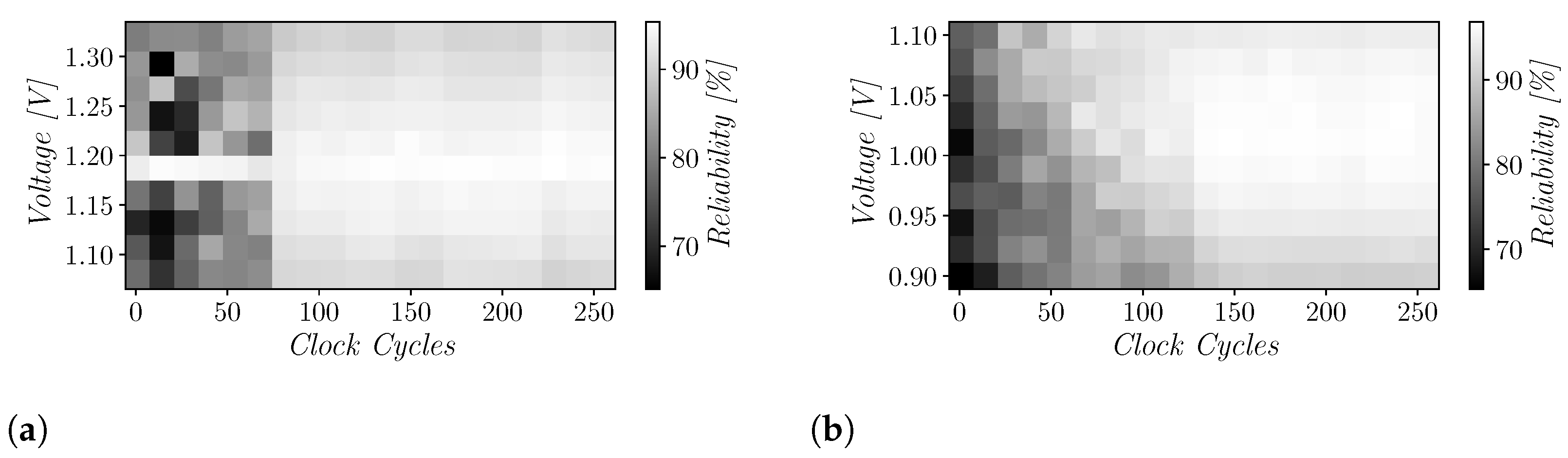
As discussed in Section 4, the proposed PUF architecture leverages on the slight differences between the propagation delay of two nominally identical paths to produce the bit response. The delays of the two paths are due to the delays of the latches and LUTs (see Equation (3)), which exhibit dependencies on process (mismatch) variations, but also on environmental conditions such as supply voltage and temperature. For given values of supply voltage and temperature, the PUF response depends only on process mismatches; however, for PUF bits in which the differences (due to mismatches) between the two delays are very small, a change in the value of the supply voltage can result in the bit-flip phenomenon [32,33], thus impacting on the response reliability. For this reason, we have carried out an in-depth study on the response reliability under voltage variations so as to asses that also when ±10% voltage variations may occur, stable bits can still be generated. In particular, since all terms in Equation (3) depend on the value of the supply voltage, we have investigated the reliability as a joint function of and the core supply voltage. The results of this analysis on the Xilinx Artix-7 are shown in Figure 6. As expected, lower supply voltage values impact negatively on the reliability, and more clock cycles are usually required to achieve a stable state in each DD-PUF cell. It is evident that some cell responses reach a soft steady-state. Therefore, small environmental variations may compromise the delay differences of the PUF cells that are used to extract response bits, and a sudden degradation of the steadiness can be observed. Hence, from a design perspective, a non-minimal value of should be chosen to mitigate the effect of low power supply voltage on the reliability of the DD-PUF. The impact of the reliability in terms of intra-class HD has been studied also from a statistical point of view, assuming that they follow Gaussian distributions [2,3], and, therefore, the sample mean and standard deviation of this metric are provided. For the Spartan-6 case, we have found = 1.63% and = 1.10%, while for the Artix-7 one, = 1.67% and = 1.19%. The result remarks that the proposed 128-bit DD-PUF design provides at each new usage a response similar to the respective GK and thus the sampled mean values are very close to the ideal ones (i.e., 0%), thus remarking the differential approach effectiveness on PUF’s reliability under PVT variations.
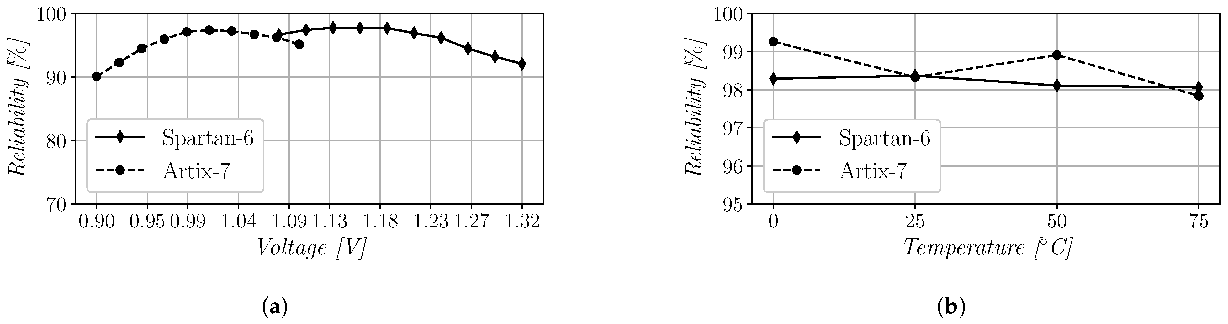
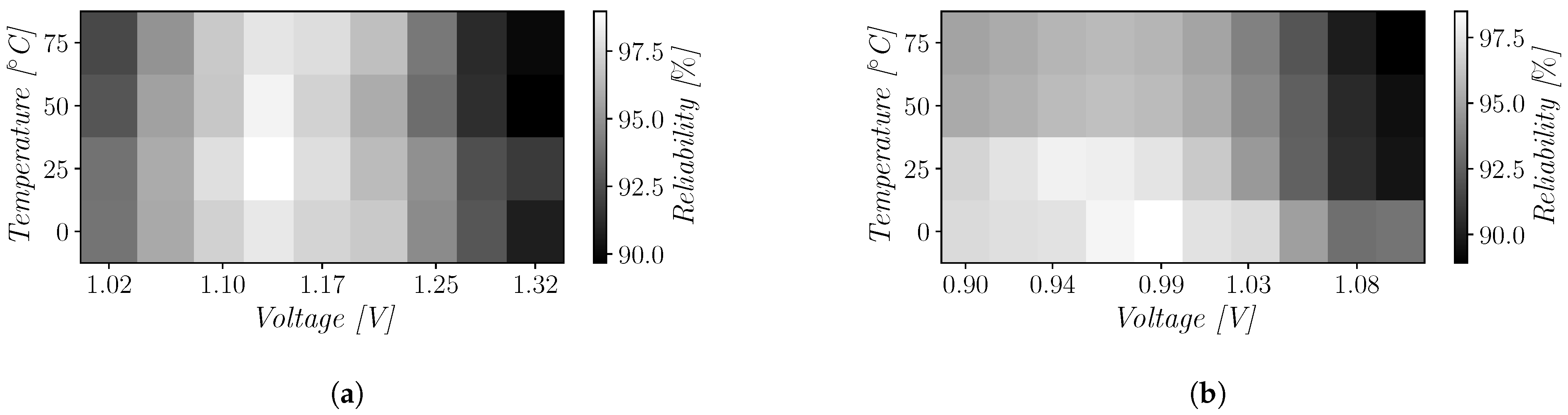
In Figure 7a, the DD-PUF reliability curves are reported as a function of the supply voltage for both FPGAs with set to 128 and 256 clock cycles for the Spartan-6 and the Artix-7 implementations, respectively. In accordance with Figure 6, best-case values have been found around nominal supply voltage, while worst-case has been found at 1.32 V for the Spartan-6 and at 0.9 V for the Artix-7. In order to cover all possible environmental conditions, we have also performed the same analysis considering the working temperature, and results are shown in Figure 7b. In both cases, the reliability variations in the [0 °C, 75 °C] range are minimal compared to the nominal case, showing that temperature is not a concern for the proposed architecture. In Figure 8, the DD-PUF reliability is reported when both temperature variations and supply voltage fluctuations are considered. This further analysis is important to fully characterize the PUF in all working condition corners. Results in Figure 7 demonstrate that both FPGA families exhibit a stronger dependency on the power supply voltage compared to the working temperature. In particular, for Spartan-6, we have found that best reliability values are provided in the range [1.13 V, 1.2 V], with negligible effect from the working temperature. On the other hand, for Artix-7, best reliability values have been found around the nominal power supply voltage, with almost no effect from working temperature. We remark that, concerning the reliability metric, in [2,3] it is recommended that a reliable PUF should be able to provide at least 90%. Therefore, in the light of the measurements results reported above, we can state that the proposed PUF is reliable in all working conditions (considering also the cross corners).
An additional issue which can impact the reliability of a PUF is aging. As discussed in [34,35], aging affects the behavior of a CMOS integrated circuit through the bias temperature instability (BTI) and the hot carrier injection (HCI) phenomenons. Both BTI and HCI result in a shift of the threshold voltage of MOS transistors and therefore in a speed degradation. Referring to RO-PUF architectures reported in [34,35] that are based on ring oscillators with different nominal frequencies, aging can be a concern. In fact, due to different degradation rates, the faster RO in a pair can become slower with the time than the other. This condition can cause a bit flip and make the PUF unreliable. The proposed DD-PUF architecture leverages on the delay difference between two signal paths which nominally exhibit the same delay and are very well matched to each other. Taking into account the extreme symmetry of the intra-connections of the two paths, it is reasonable to assume that aging affects elements in a similar way. Moreover, the compactness of the DD-PUF macro should bolster aforementioned considerations given that, compared to RO-PUF macros, results much more compact (half-slice compared with much more slices of RO-based architectures) and consequently aging effects would be considered constant on such a low area. Therefore, the aging effect on both paths would be considered (at a first glance) as “common mode" variations that are canceled by taking the paths’ delay difference. Hence, we believe that the aging impact on DD-PUF would lead to results comparable to those observed under temperature fluctuations because both aging and temperature imply a threshold voltage shift. In conclusion, since the DD-PUF has been found robust against temperature variations, we expect a good reliability also in the regard of aging effects.
5.3. Randomness and Uniformity Results
With the aim of verifying the usability of our DD-PUF, we have performed NIST tests discussed in Section 3 for both FPGA families. We have investigated the quality of the randomness given by the 128-bit responses of 16 devices for each FPGA family. It has been found that each device produces p-values greater than 0.01. Consequently the test is undergone for both FPGA families with pass-rate proportions greater than the minimum required. p-values obtained from the GK response are reported in Table 2. The average value of the bias has been computed considering the mean value of the 16 devices’ responses for both families. It has been found that the 1/0 bias of the DD-PUF extracted from the Spartan-6 design is about 48.47% with a standard deviation of 4.94% whereas the Artix-7 design provides a mean value of 50.59% with a standard-deviation of 5.37%. Furthermore, experimental results on Spartan-6 devices pointed out that the best uniformity is reached on 3 out of 16 devices, showing a 49.22% and 50.78% of 1/0 bias. Moreover, 3 of the 16 Artix-7 FPGAs have provided a 1/0 bias of 50%. These results show that the proposed DD-PUF cell designs are able to fully exploit process and mismatch variations only, and clearly, no evidence of systematic bias have been found. It is therefore reasonable to conclude that with a larger number of devices, the bias would converge to a mean value closer to the ideal one (i.e., 50%) for both FPGA families.
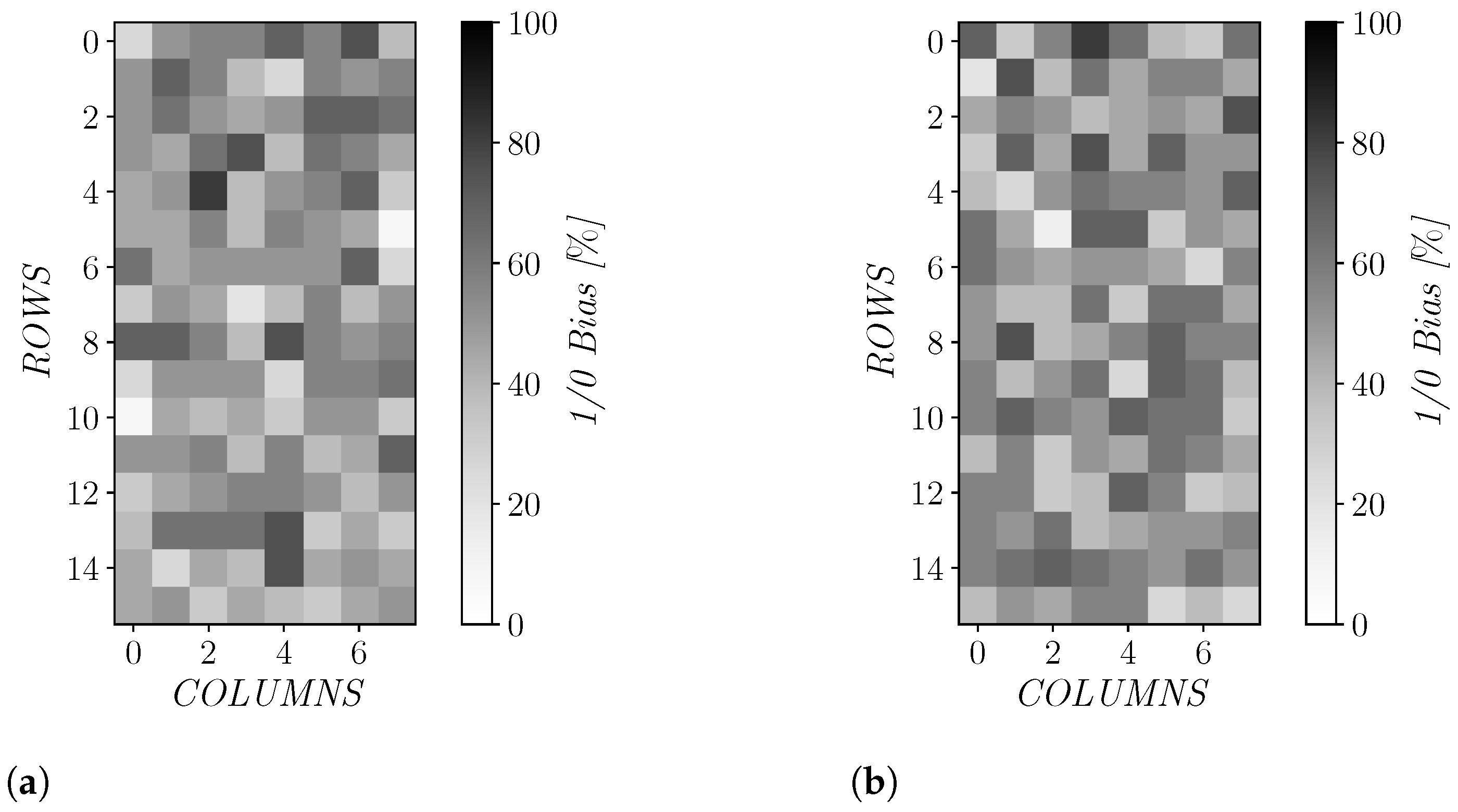
The 1/0 bias has been investigated even at single-bit level across the pool of 16 devices per FPGA family. This study aims at identifying spotting bits that are prone to provide always the same value across different devices (also known as dark bits). Results of the single-bit level 1/0 bias are shown in Figure 9. As it can be observed, in all bit-locations an approximately uniform 1/0 distribution has been obtained. We remark that the responses taken into account are sampled out-of-the-box without post-processing or post-elaboration techniques.
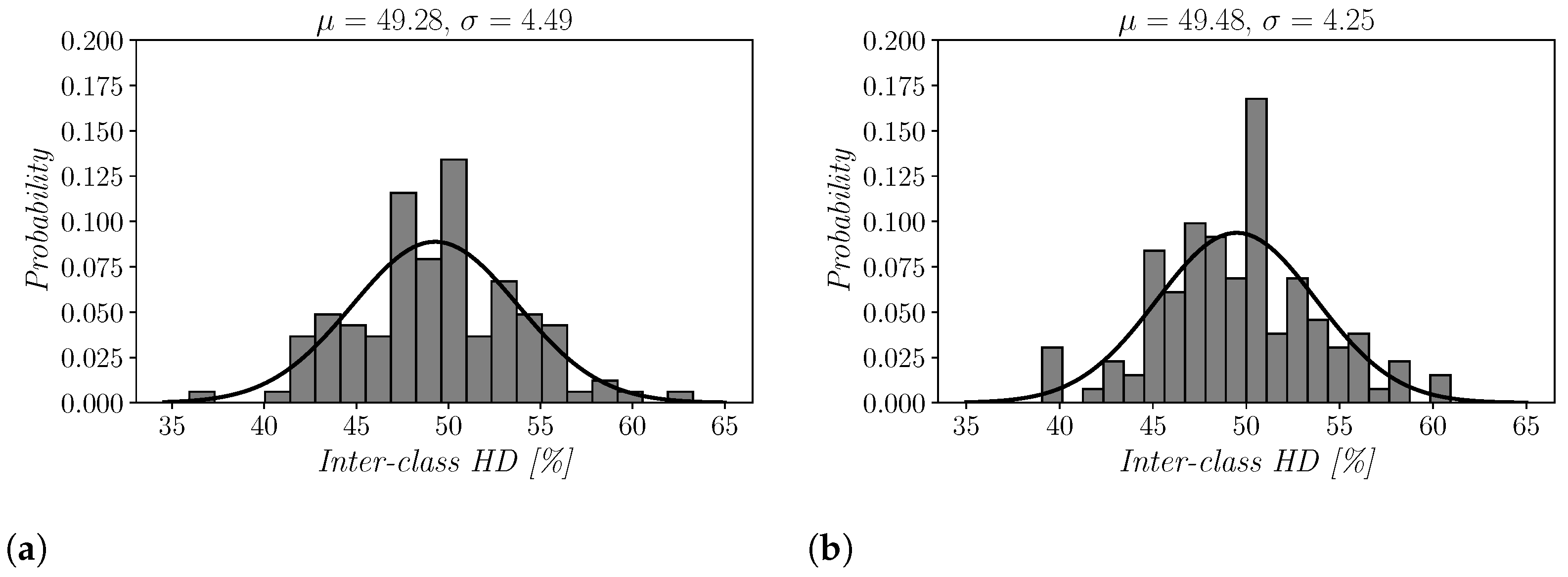
5.4. Uniqueness Results
The inter-class HD of the Xilinx Spartan-6 pool is shown in Figure 10a, with values on the x-axis reported as percentage among 128-bit responses. We have found a sample mean value of the inter-class HD of 49.28% with a standard deviation of 4.49%. Similarly, the inter-class HD for the Artix-7 pool is reported in Figure 10b showing an average value of about 49.48% with a standard deviation of 4.25%. As can be seen, the obtained value for both FPGA families is very close with the ideal 50%. These results remark that the proposed DD-PUF architecture is able to extract entropy mostly due to manufacturing process. No structured artifacts have been found in our statistical analysis of responses collected from different devices implementing the same circuit. Hence, the DD-PUF has shown a strongly repeatable design across two different FPGA families.
6. Comparison with State of the Art
The proposed DD-PUF has been compared against the state of the art and a summary of this comparison is reported in Table 3. From Table 3 it is evident that the most compact PUF, among all previously published ones, is the Pico-PUF, which requires 128 slices and 128 CLBs to generate a 128-bit response. To the best of our knowledge, the DD-PUF has improved the resource footprint of the Pico-PUF, while deploying an highly reliable PUF primitive. In fact, the proposed DD-PUF requires only 32 CLBs, hence 64 slices, to generate a 128-bit response, thus the resource consumption has been extremely improved. Looking at the other figures of merit, the proposed 128-bit DD-PUF designs exhibit a reliability of 98.33% and 98.37% and a uniqueness of 49.48% and 49.28% on the Xilinx Artix-7 and Spartan-6, respectively, that are very close to the ideal ones, thus confirming that the remarkable improvement in density has been achieved without sacrificing performance.
7. Conclusions
In this work, we presented a novel ultra-compact PUF, the Delay Difference PUF (DD-PUF). The proposed architecture has been successfully implemented on 16 Xilinx Spartan-6 and 16 Xilinx Artix-7 FPGAs, as a 128-bit primitive. The novel FPGA-compatible PUF exploits the delay difference of two nominally identical paths, each of them consisting in an inverter and a D-type latch. A single DD-PUF cell digitizes the delay difference of its two paths as the differential value of the steady state that is reached after an oscillatory phase. The placement and the routing of a dual-bit DD-PUF cell macro have been optimized in order to fully exploit the mismatch and process variations within the two considered FPGA families. The analysis of the performance of the proposed architecture has been carried out considering supply voltage variations in a range around the nominal voltage, and in a wide working temperature range. Important metrics such as reliability, uniqueness and uniformity have been evaluated in a plethora of different working conditions, covering a full PVT analysis of the DD-PUF on the two aforementioned FPGA platforms. The reliability analysis of the proposed designs has shown that a value of ∼98% can be easily reached in nominal conditions on both kind of devices. The uniqueness evaluation of pools of 16 devices per FPGA family has shown that the novel PUF is able to guarantee a uniqueness of 49.28% on the Xilinx Spartan-6 and 49.48% on the Artix-7, clearly, very close to the ideal 50%. In addition, responses of the proposed architecture have been validated from a randomicity viewpoint, by means of NIST tests, showing that the DD-PUF is able to pass all tests. Giving the remarkable small resource footprint of 0.5 slice/bit requirement of a DD-PUF cell, the proposed architecture represents the most compact FPGA-compatible weak PUF in the literature, reducing the size of the state of the art by a factor of two. Furthermore, the novel PUF architecture does not suffer o from bias due to unfortunate FPGA sites, hence, it does not require any particular macro placement constraints.
Author Contributions
Conceptualization, R.D.S.; methodology, R.D.S., D.B., G.S.; software, R.D.S., D.B.; validation, R.D.S., D.B., G.S.; formal analysis, R.D.S., D.B.; investigation, R.D.S., D.B., G.S.; resources, G.S.; data curation, R.D.S., D.B.; writing—original draft preparation, R.D.S.; writing—review and editing, D.B., G.S.; visualization, G.S.; supervision, G.S.; funding acquisition, G.S. All authors have read and agreed to the published version of the manuscript.
Funding
This research received no external funding.
Institutional Review Board Statement
Not applicable.
Informed Consent Statement
Not applicable.
Data Availability Statement
The data presented in this study are available in article.
Conflicts of Interest
The authors declare no conflict of interest.
References
- Rührmair, U.; Holcomb, D.E. PUFs at a glance. In Proceedings of the 2014 Design, Automation Test in Europe Conference Exhibition (DATE), Dresden, Germany, 24–28 March 2014; pp. 1–6. [Google Scholar] [CrossRef]
- Böhm, C.; Hofer, M. Physical Unclonable Functions in Theory and Practice; Springer Science & Business Media: New York, NY, USA, 2012. [Google Scholar]
- Halak, B. Physically Unclonable Functions: From Basic Design Principles to Advanced Hardware Security Applications; Springer: Berlin/Heidelberg, Germany, 2018. [Google Scholar]
- Qureshi, M.A.; Munir, A. PUF-RAKE: A PUF-based Robust and Lightweight Authentication and Key Establishment Protocol. IEEE Trans. Dependable Secur. Comput. 2021. [Google Scholar] [CrossRef]
- Johnson, A.P.; Chakraborty, R.S.; Mukhopadhyay, D. A PUF-enabled secure architecture for FPGA-based IoT applications. IEEE Trans. Multi-Scale Comput. Syst. 2015, 1, 110–122. [Google Scholar] [CrossRef]
- Chatterjee, U.; Govindan, V.; Sadhukhan, R.; Mukhopadhyay, D.; Chakraborty, R.S.; Mahata, D.; Prabhu, M.M. Building PUF based authentication and key exchange protocol for IoT without explicit CRPs in verifier database. IEEE Trans. Dependable Secur. Comput. 2018, 16, 424–437. [Google Scholar] [CrossRef]
- Suh, G.E.; Devadas, S. Physical Unclonable Functions for Device Authentication and Secret Key Generation. In Proceedings of the 2007 44th ACM/IEEE Design Automation Conference, San Diego, CA, USA, 4–8 June 2007; pp. 9–14. [Google Scholar]
- Yilmaz, Y.; Gunn, S.R.; Halak, B. Lightweight PUF-based authentication protocol for IoT devices. In Proceedings of the 2018 IEEE 3rd International Verification and Security Workshop (IVSW), Costa Brava, Spain, 2–4 July 2018; pp. 38–43. [Google Scholar]
- Gu, C.; Hanley, N.; O’Neill, M. FPGA-based strong PUF with increased uniqueness and entropy properties. In Proceedings of the 2017 IEEE International Symposium on Circuits and Systems (ISCAS), Baltimore, MD, USA, 28–31 May 2017; pp. 1–4. [Google Scholar] [CrossRef] [Green Version]
- Gu, C.; Chang, C.H.; Liu, W.; Hanley, N.; Miskelly, J.; O’Neill, M. A large-scale comprehensive evaluation of single-slice ring oscillator and PicoPUF bit cells on 28-nm Xilinx FPGAs. J. Cryptogr. Eng. 2020, 11, 1–12. [Google Scholar]
- Guajardo, J.; Kumar, S.S.; Schrijen, G.J.; Tuyls, P. FPGA Intrinsic PUFs and Their Use for IP Protection. In Proceedings of the Cryptographic Hardware and Embedded Systems-CHES 2007, 9th International Workshop, Vienna, Austria, 10–13 September 2007; pp. 63–80. [Google Scholar]
- Holcomb, D.E.; Burleson, W.P.; Fu, K. Power-Up SRAM State as an Identifying Fingerprint and Source of True Random Numbers. IEEE Trans. Comput. 2009, 58, 1198–1210. [Google Scholar] [CrossRef]
- Kumar, S.S.; Guajardo, J.; Maes, R.; Schrijen, G.J.; Tuyls, P. The Butterfly PUF: Protecting IP on every FPGA. In Proceedings of the IEEE International Workshop on Hardware-Oriented Security and Trust, HOST 2008, Anaheim, CA, USA, 9 June 2008; pp. 67–70. [Google Scholar]
- Merli, D.; Heyszl, J.; Heinz, B.; Schuster, D.; Stumpf, F.; Sigl, G. Localized electromagnetic analysis of RO PUFs. In Proceedings of the 2013 IEEE International Symposium on Hardware-Oriented Security and Trust, HOST 2013, Austin, TX, USA, 2–3 June 2013; pp. 19–24. [Google Scholar]
- Bossuet, L.; Ngo, X.T.; Cherif, Z.; Fischer, V. A PUF Based on a Transient Effect Ring Oscillator and Insensitive to Locking Phenomenon. IEEE Trans. Emerg. Top. Comput. 2014, 2, 30–36. [Google Scholar] [CrossRef]
- Lim, D.; Lee, J.W.; Gassend, B.; Suh, G.E.; van Dijk, M.; Devadas, S. Extracting secret keys from integrated circuits. IEEE Trans. Very Large Scale Integr. (VLSI) Syst. 2005, 13, 1200–1205. [Google Scholar] [CrossRef]
- Nguyen, P.H.; Sahoo, D.P.; Jin, C.; Mahmood, K.; Rührmair, U.; van Dijk, M. The Interpose PUF: Secure PUF Design against State-of-the-art Machine Learning Attacks. IACR Trans. Cryptogr. Hardw. Embed. Syst. 2019, 2019, 243–290. [Google Scholar] [CrossRef]
- Gu, C.; O’Neill, M. Ultra-compact and robust FPGA-based PUF identification generator. In Proceedings of the 2015 IEEE International Symposium on Circuits and Systems (ISCAS), Lisbon, Portugal, 24–27 May 2015; pp. 934–937. [Google Scholar] [CrossRef]
- Gu, C.; Murphy, J.; O’Neill, M. A unique and robust single slice FPGA identification generator. In Proceedings of the 2014 IEEE International Symposium on Circuits and Systems (ISCAS), Melbourne, VIC, Australia, 1–5 June 2014; pp. 1223–1226. [Google Scholar]
- Gu, C.; Hanley, N.; O’Neill, M. Improved reliability of FPGA-based PUF identification generator design. ACM Trans. Reconfigurable Technol. Syst. (TRETS) 2017, 10, 1–23. [Google Scholar] [CrossRef] [Green Version]
- Marchand, C.; Bossuet, L.; Mureddu, U.; Bochard, N.; Cherkaoui, A.; Fischer, V. Implementation and Characterization of a Physical Unclonable Function for IoT: A Case Study With the TERO-PUF. IEEE Trans. Comput.-Aided Des. Integr. Circuits Syst. 2018, 37, 97–109. [Google Scholar] [CrossRef] [Green Version]
- Tebelmann, L.; Pehl, M.; Immler, V. Side-channel analysis of the TERO PUF. In International Workshop on Constructive Side-Channel Analysis and Secure Design; Springer: Berlin/Heidelberg, Germany, 2019; pp. 43–60. [Google Scholar]
- Yin, C.E.; Qu, G. Improving PUF security with regression-based distiller. In Proceedings of the 50th Annual Design Automation Conference 2013, DAC’13, Austin, TX, USA, 29 May–7 June 2013; pp. 1–6. [Google Scholar]
- Bassham, L.; Rukhin, A.; Soto, J.; Nechvatal, J.; Smid, M.; Leigh, S.; Levenson, M.; Vangel, M.; Heckert, N.; Banks, D. A Statistical Test Suite for Random and Pseudorandom Number Generators for Cryptographic Applications. In Proceedings of the Special Publication (NIST SP), National Institute of Standards and Technology, Gaithersburg, MD, USA, 16 September 2010. [Google Scholar]
- Gao, M.; Lai, K.; Qu, G. A highly flexible ring oscillator PUF. In Proceedings of the 51st Annual Design Automation Conference, San Francisco, CA, USA, 1–5 June 2014; pp. 1–6. [Google Scholar]
- Xu, T.; Potkonjak, M. Robust and flexible FPGA-based digital PUF. In Proceedings of the 2014 24th International Conference on Field Programmable Logic and Applications (FPL), Munich, Germany, 2–4 September 2014; pp. 1–6. [Google Scholar]
- Yin, C.E.; Qu, G.; Zhou, Q. Design and implementation of a group-based RO PUF. In Proceedings of the 2013 Design, Automation & Test in Europe Conference & Exhibition (DATE), Grenoble, France, 18–22 March 2013; pp. 416–421. [Google Scholar]
- Avaroğlu, E. The implementation of ring oscillator based PUF designs in Field Programmable Gate Arrays using of different challenge. Phys. A Stat. Mech. Its Appl. 2020, 546, 124291. [Google Scholar] [CrossRef]
- Reyneri, L.; Del Corso, D.; Sacco, B. Oscillatory metastability in homogeneous and inhomogeneous flip-flops. IEEE J. Solid-State Circuits 1990, 25, 254–264. [Google Scholar] [CrossRef]
- Xilinx. Spartan-6 FPGA Configurable Logic Block UG384 (v1.1), 23 February 2010. Available online: https://dokumen.tips/documents/xilinx-ug384-spartan-6-fpga-configurable-logic-block-user-guide.html (accessed on 1 September 2021).
- Bellizia, D.; Bongiovanni, S.; Olivieri, M.; Scotti, G. SC-DDPL: A Novel Standard-Cell Based Approach for Counteracting Power Analysis Attacks in the Presence of Unbalanced Routing. IEEE Trans. Circuits Syst. I Regul. Pap. 2020, 67, 2317–2330. [Google Scholar] [CrossRef]
- Eiroa, S.; Castro, J.; Martínez-Rodríguez, M.C.; Tena, E.; Brox, P.; Baturone, I. Reducing bit flipping problems in SRAM physical unclonable functions for chip identification. In Proceedings of the 2012 19th IEEE International Conference on Electronics, Circuits, and Systems (ICECS 2012), Seville, Spain, 9–12 December 2012; pp. 392–395. [Google Scholar]
- Selimis, G.; Konijnenburg, M.; Ashouei, M.; Huisken, J.; de Groot, H.; van der Leest, V.; Schrijen, G.J.; van Hulst, M.; Tuyls, P. Evaluation of 90nm 6T-SRAM as physical unclonable function for secure key generation in wireless sensor nodes. In Proceedings of the 2011 IEEE International Symposium of Circuits and Systems (ISCAS), Rio de Janeiro, Brazil, 15–18 May 2011; pp. 567–570. [Google Scholar]
- Chowdhury, S.; Xu, X.; Tehranipoor, M.; Forte, D. Aging resilient RO PUF with increased reliability in FPGA. In Proceedings of the 2017 International Conference on ReConFigurable Computing and FPGAs (ReConFig), Cancun, Mexico, 4–6 December 2017; pp. 1–7. [Google Scholar]
- Rahman, M.T.; Rahman, F.; Forte, D.; Tehranipoor, M. An Aging-Resistant RO-PUF for Reliable Key Generation. IEEE Trans. Emerg. Top. Comput. 2016, 4, 335–348. [Google Scholar] [CrossRef]
- Yamamoto, D.; Sakiyama, K.; Iwamoto, M.; Ohta, K.; Ochiai, T.; Takenaka, M.; Itoh, K. Uniqueness Enhancement of PUF Responses Based on the Locations of Random Outputting RS Latches. In Cryptographic Hardware and Embedded Systems—CHES 2011; Preneel, B., Takagi, T., Eds.; Springer: Berlin/Heidelberg, Germany, 2011; pp. 390–406. [Google Scholar]
- Maes, R.; Tuyls, P.; Verbauwhede, I. Intrinsic PUFs from flip-flops on reconfigurable devices. In Proceedings of the 3rd Benelux Workshop on Information and System Security (WISSec 2008), Eindhoven, The Netherlands, 13–14 November 2008; Volume 17, p. 2008. [Google Scholar]
Figure 1.
FPGA-compatible state-of-the-art PUF architecture: (a) Butterfly-PUF (BPUF), (b) Arbiter-PUF (APUF), (c) Pico-PUF, (d) Ring-Oscillator PUF (RO-PUF) and (e) TERO-PUF.
Figure 1.
FPGA-compatible state-of-the-art PUF architecture: (a) Butterfly-PUF (BPUF), (b) Arbiter-PUF (APUF), (c) Pico-PUF, (d) Ring-Oscillator PUF (RO-PUF) and (e) TERO-PUF.

Figure 2.
Architecture of the Delay Difference PUF (a) and timing diagram of the excitation sequence (b).
Figure 2.
Architecture of the Delay Difference PUF (a) and timing diagram of the excitation sequence (b).

Figure 3.
Routing of 4 DD-PUF cells on the Xilinx Spartan-6 (a) and Artix-7 (b).

Figure 4.
Block scheme of the inter-chip validation testbed.

Figure 5.
Reliability and bias as function of the length of the evaluation phase expressed as number of clock cycles, in nominal environmental conditions for the Xilinx Spartan-6 (a) and Artix-7 (b).
Figure 5.
Reliability and bias as function of the length of the evaluation phase expressed as number of clock cycles, in nominal environmental conditions for the Xilinx Spartan-6 (a) and Artix-7 (b).

Figure 6.
Reliability values of the 128-bit DD-PUF as function of power supply voltage and evaluation phase’s duration for the Xilinx Spartan-6 (a) and Artix-7 (b) FPGAs.
Figure 6.
Reliability values of the 128-bit DD-PUF as function of power supply voltage and evaluation phase’s duration for the Xilinx Spartan-6 (a) and Artix-7 (b) FPGAs.

Figure 7.
Reliability as function of power supply voltage (a) and working temperature (b) for Xilinx Spartan-6 and Artix-7.
Figure 7.
Reliability as function of power supply voltage (a) and working temperature (b) for Xilinx Spartan-6 and Artix-7.

Figure 8.
Reliability as a joint function of power supply voltage and working temperature for the Xilinx Spartan-6 (a) and Xilinx Artix-7 (b).
Figure 8.
Reliability as a joint function of power supply voltage and working temperature for the Xilinx Spartan-6 (a) and Xilinx Artix-7 (b).

Figure 9.
Bit-bias computed on 16 devices: Xilinx Spartan-6 (a) and Xilinx Artix-7 (b).

Figure 10.
Histograms reporting inter-class HD values computed on Xilinx Spartan-6 (a) and Xilinx Artix-7 (b).
Figure 10.
Histograms reporting inter-class HD values computed on Xilinx Spartan-6 (a) and Xilinx Artix-7 (b).


Table 1.
Reports of delay differences on critical nets (worst-case) of a 2-bit DD-PUF macro on the Xilinx Spartan-6 and Xilinx Artix-7 FPGAs.
Table 1.
Reports of delay differences on critical nets (worst-case) of a 2-bit DD-PUF macro on the Xilinx Spartan-6 and Xilinx Artix-7 FPGAs.
| Slice Position | Net-Differences | Spartan-6 Delay [ps] | Artix-7 Delay [ps] |
|---|---|---|---|
| UPPER | Q1,A-Q2,A | 43 | 1 |
| UPPER | Q1,B-Q2,B | 15 | 1 |
| LOWER | Q1,A-Q2,A | 37 | 4 |
| LOWER | Q1,B-Q2,B | 48 | 4 |
Table 2.
Summary of NIST test suite.
| Mono-Bit Test | Block Freq. Test | Cum. Test | Run Test | Longest Run Test | Approx. Entropy Test | |
|---|---|---|---|---|---|---|
| Spartan-6 | 0.860 | 0.687 | 0.819 | 0.077 | 0.249 | 0.334 |
| Artix-7 | 1.000 | 0.932 | 0.998 | 0.157 | 0.365 | 0.409 |
| Pass/Fail | ✓ | ✓ | ✓ | ✓ | ✓ | ✓ |
Table 3.
FPGA-Implemented Weak-PUF Comparison.
| This Work | This Work | [10] | [20] | [19] | [36] | [37] | [11] | [7] | [13] | |
|---|---|---|---|---|---|---|---|---|---|---|
| Year | 2021 | 2021 | 2020 | 2017 | 2014 | 2011 | 2008 | 2007 | 2007 | 2006 |
| PUF | DD | DD | Single Slice RO | Pico | Pico | Latch | Flip-Flop | SRAM | RO | Butterfly |
| Device | Artix-7 | Spartan-6 | Artix-7 | Artix-7 | Spartan-6 | Spartan-3E | Virtex-2 Pro | FPGA | Virtex-4 | Virtex-5 |
| Uniqueness [%] | 49.48 | 49.28 | 48.05 | 49.90 | 48.52 | 46.00 | ≈50.00 * | 49.97 | 46.15 | ≈50 |
| Reliability [%] | 98.33 | 98.37 | 99.30 | 94.53 | 93.00 | >87 | >95.00 * | >88 | 99.52 | 94.00 |
| Response-bit | 128 | 128 | 128 | 128 | 128 | 128 | 4096 | 128 | 128 | 64 |
| CLB/bit | 1/4 | 1/4 | 1 | 1 | 1 | - | - | - | - | 1 |
| Slice/bit | 1/2 | 1/2 | 1 | 1 | 1 | 2 | 1 | - | - | >2 |
| Res. | 64 slices | 64 slices | >256 slices | 128 slices | 128 slices | 256 slices | 4096 flip-flops | 4600 SRAM | 16x64 array | >128 slices |
* post-processing required; 1024 ROs each of one designed with five inverters and 1 AND; additional logic required; under temperature variations.
Publisher’s Note: MDPI stays neutral with regard to jurisdictional claims in published maps and institutional affiliations. |
© 2021 by the authors. Licensee MDPI, Basel, Switzerland. This article is an open access article distributed under the terms and conditions of the Creative Commons Attribution (CC BY) license (https://creativecommons.org/licenses/by/4.0/).
Share and Cite
MDPI and ACS Style
Della Sala, R.; Bellizia, D.; Scotti, G. A Novel Ultra-Compact FPGA PUF: The DD-PUF. Cryptography 2021, 5, 23. https://0-doi-org.brum.beds.ac.uk/10.3390/cryptography5030023
AMA Style
Della Sala R, Bellizia D, Scotti G. A Novel Ultra-Compact FPGA PUF: The DD-PUF. Cryptography. 2021; 5(3):23. https://0-doi-org.brum.beds.ac.uk/10.3390/cryptography5030023
Chicago/Turabian StyleDella Sala, Riccardo, Davide Bellizia, and Giuseppe Scotti. 2021. "A Novel Ultra-Compact FPGA PUF: The DD-PUF" Cryptography 5, no. 3: 23. https://0-doi-org.brum.beds.ac.uk/10.3390/cryptography5030023