Article

Monte Carlo Modeling and Design of Photon Energy Attenuation Layers for >10× Quantum Yield Enhancement in Si-Based Hard X-ray Detectors

1
Thayer School of Engineering, Dartmouth College, Hanover, NH 03755, USA
2
Los Alamos National Laboratory, Los Alamos, NM 87545, USA
*
Authors to whom correspondence should be addressed.
Submission received: 7 April 2021 / Revised: 28 April 2021 / Accepted: 28 April 2021 / Published: 30 April 2021

Abstract

:
High-energy (>20 keV) X-ray photon detection at high quantum yield, high spatial resolution, and short response time has long been an important area of study in physics. Scintillation is a prevalent method but limited in various ways. Directly detecting high-energy X-ray photons has been a challenge to this day, mainly due to low photon-to-photoelectron conversion efficiencies. Commercially available state-of-the-art Si direct detection products such as the Si charge-coupled device (CCD) are inefficient for >10 keV photons. Here, we present Monte Carlo simulation results and analyses to introduce a highly effective yet simple high-energy X-ray detection concept with significantly enhanced photon-to-electron conversion efficiencies composed of two layers: a top high-Z photon energy attenuation layer (PAL) and a bottom Si detector. We use the principle of photon energy down conversion, where high-energy X-ray photon energies are attenuated down to ≤10 keV via inelastic scattering suitable for efficient photoelectric absorption by Si. Our Monte Carlo simulation results demonstrate that a 10–30× increase in quantum yield can be achieved using PbTe PAL on Si, potentially advancing high-resolution, high-efficiency X-ray detection using PAL-enhanced Si CMOS image sensors.

1. Introduction

Since the discovery of X-rays by Roentgen, the continuous expansion of X-ray technology has transformed our society from materials science to biomedical applications. However, the capability gap for the efficient and direct detection of high-energy X-ray photons in the 20–50 keV range and beyond is challenging, which will prevent further advancements in rising fields of technology such as the generic platform of X-ray imaging sensor technology and the next generation of synchrotron light source facilities [1,2,3,4,5]. Scintillator-based methods are widely used in these types of facilities and high-energy X-ray detection technologies; however, they have major limitations such as decay time response and light yield [6,7]. Furthermore, the spatial resolution of such a method is limited due to the thickness required for the scintillator to absorb high-energy X-ray photons. There are also commercially available state-of-the-art X-ray detectors based on Si direct detection. For instance, the Si charge-coupled device (CCD) and CMOS image sensors, which are commercially available in many formats, are known to be efficient in X-ray photon energies ≤10 keV and are typically most efficient in the 100 eV–10 keV range [8]. However, beyond this energy, Si is notoriously inefficient in detecting X-rays as it is known to transmit the majority of high-energy photons [8,9].
There have been considerable efforts to overcome these issues and limitations by many researchers. One example of such work is a two-layer high-energy X-ray detector structure comprising a cm-scale-area and mm-scale-thick metal buildup layer on a semiconductor thin-film to obtain high energy deposition and high dose delivery for radiation therapy [10,11]. However, because this type of work could be unsuitable with small-form-factor commercial-off-the-shelf technologies (COTs), such as CMOS image sensors (CIS) and quanta image sensors (QIS) as mm- and cm-scale metal thickness, could cause significant X-ray crosstalk to adjacent pixels that might be 20–50 µm in pixel pitch [12]. Furthermore, the claim that has been made for the underlying principle of this prior work is that high-energy X-ray photons are converted to secondary electrons through Compton interaction in the top mm-scale metal buildup layer followed by the transport of these secondary electrons into the semiconductor thin-film layer for electron detection [10]. While this concept is intriguing, one questionable critical matter for our energy range of interest is that if the incident X-ray photon energies are relatively low compared to those intended for medical applications (MeV range), the low-energy secondary electrons (~1–10 keV range) could never escape the thick metal buildup layer after absorbing an X-ray photon as the corresponding electron mean free paths are rather small (<1 μm) in many materials [13]; therefore, the electrons could never make it to the bottom semiconductor thin-film layer for electron detection. Because of the relatively small travel ranges of electrons, even if the semiconductor thin-film layer for electron detection is decreased to μm-scale in terms of thickness, it is likely that the secondary electrons could still remain in the mm-scale-thick metal buildup layer. Similar to this example, a Si X-ray CT detector for MeV-range applications that utilizes 200 µm-thick tungsten (W) metal sheet as a down-converter placed between two Si detectors has been previously developed and takes advantage of secondary electrons [14]. However, due to the thickness of the W layer, such a concept would be incompatible with and unideal for COTS CIS and QIS.
Another class of work focuses on structured photocathode designs that depend on external photoemission, the angle of X-ray photon absorption, and the collection of electrons produced by photon interactions using an external electric field. This approach has demonstrated up to 5% quantum yield (QY), which is defined [15,16,17] as:
Q Y = #   o f   p r i m a r y   p h o t o e l e c t r o n s   c o l l e c t e d #   o f   i n c i d e n t   p h o t o n s ,
In this article, primary photoelectrons are defined as those directly excited by X-ray photons prior to impact ionization, while secondary photoelectrons are those created by primary photoelectrons via impact ionization [16].
For almost 4 decades, QY from external photoemission has been roaming around 1–1.5%; therefore, the increase to 5% is commendable [17,18]. While the technique to reach the 5% QY is claimed to be suitable for higher X-ray photon energies at around 20–30 keV, one should note that the X-ray photon absorption coefficient will decay rapidly with the increase in incident photon energies, which eventually will lead to lower QY at higher incident photon energies [8,9,19]. Therefore, this technique may not be extended to higher X-ray photon energy ranges of interest (i.e., >20 keV).
There also have been numerous recent advances in the development of high-Z X-ray detectors such as Ge- and Cr compensated GaAs (GaAs:Cr)-based detectors [20,21,22]. However, these materials have considerable fabrication drawbacks. For instance, there is a necessity to eliminate thermally generated carriers by cooling the material down to cryogenic temperatures for Ge-based high-energy X-ray detectors [20,21]. Furthermore, while GaAs:Cr-based detectors seem favorable, fabrication yield of good quality GaAs can be difficult [22].
There also have been significant advances in CdTe-based detectors, which is now one of the most common materials used in high-energy X-ray detection. Some of the CdTe-based detectors report 75–100% efficiency at 20–50 keV range; however, to reach such high efficiency, the thicknesses of CdTe must be in hundreds of microns and commercial state-of-the-art CdTe-based detectors currently use mm-scale-thick CdTe layers [10,23,24]. It should also be stressed that unlike Si CIS-based devices, CdTe-based detectors cannot be easily scaled into large arrays. Moreover, large semiconductor material thicknesses will ultimately restrict the response time of the devices. As a result, relatively thick film applications will not be ideal and suitable for small-form-factor COTs CIS and QIS-based devices.
In addition to the aforementioned research work and advances in high-energy X-ray detection methods, Si calorimeters have also been in extensively studied. While there have been significant efforts on the development of the Si calorimeters, including integration with CMOS-based sensors, they are typically for large-area Si applications (i.e., cm2 and m2) and also for considerably higher energy photons or particles, mostly in the GeV range [25].
Scintillators are known to have high absorption efficiencies. Similar to recent developments in CdTe-based detectors, the absorption efficiencies may be between 50% and 100%. Similar to CdTe-based detectors, the high efficiencies are reached by using hundreds of microns of scintillation materials and in many cases, they are achieved by using mm- and cm-thick layers [26,27]. However, besides absorption efficiency, the total efficiency of scintillators is important to be discussed. To calculate the total efficiency TE of scintillators, the following equation must be used:
T E = D x × A × E x × I Q E
where Dx is detector efficiency at an incident photon energy, A is absorption efficiency at an incident photon energy, Ex is first-order light extraction efficiency limited by total internal reflection, which is 1 / ( 4 n 2 ) , n being the refractive index, and IQE is quantum efficiency of converting to UV/visible photons [26]. A very commonly used state-of-the-art scintillator is NaI(TI). When this scintillator is considered with 60 keV incident energy, 2 in diameter, and 2 in thickness, the corresponding values of Equation (2) are Dx = 0.97, A = 1, Ex = 0.073, and IQE = 0.15 to 0.30 [26,27]. Using these values, the TE of NaI (TI) scintillators with 60 keV incident X-ray photon energy can range between 1.06% and 2.12%. The low TE of a relatively thick scintillator describes the limitation of scintillators and if this thickness is decreased to µm-scale as our proposed concept, the TE will be significantly exacerbated.
As it is demonstrated by the calculation above, the inadequate total efficiency is caused by the exceptionally low light extraction efficiency, which is limited by total internal reflection. Not only will the total efficiency be considerably reduced by such restriction, but also signal-to-noise ratio [28]. Recent efforts have sought to enhance the light extraction efficiency. A prime example of such efforts is the development of Bi4Ge3O12 scintillators with arrays of well-designed polymethyl-methacrylate (PMMA) hemispherical microlens that have led to a notable increase in the light extraction efficiency [28]. However, this noteworthy increase was only by a factor of 1.94–2.59, which would still leave the total efficiency substandard.

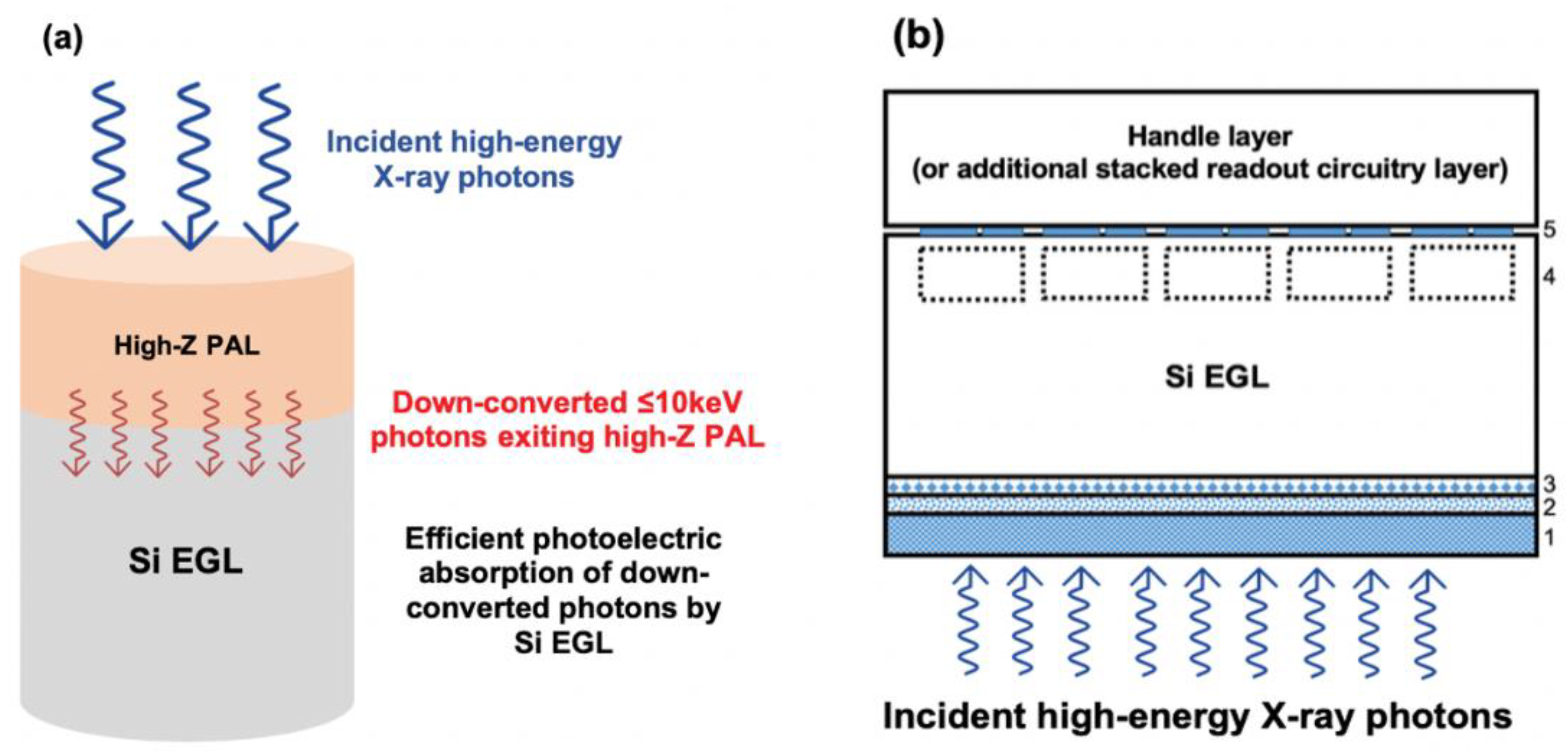
2. Concept of Photon Attenuation Layer (PAL)

In this article, we present a new concept for the direct detection of high-energy X-ray photons by using a high-Z thin film, the “photon attenuation layer” (PAL), to attenuate the incident photon energy below 10 keV, thereby allowing more efficient absorption of down-converted X-ray photons by Si detectors underneath, or more generally, an “electron generation layer” (EGL). Throughout this article, the definition of QY corresponds to Equation (1), where the primary photoelectrons collected are those in Si EGL. Our Monte Carlo simulation results and analyses using Monte Carlo N-Particle Software (MCNP6.2) demonstrates 10–30× QY enhancement in the X-ray photon energy range of 20–50 keV. The conceptual design consists of two layers: a high-Z material PAL and a Si EGL, as shown in Figure 1a. The two types of primary interaction mechanisms in PAL-EGL are photon energy down conversion due to inelastic scattering, followed by photoelectric absorption [29] (Figure 1a). Because X-ray absorption and scattering cross-sections increase as atomic numbers increase, high-Z materials are chosen for the PAL [30]. In PAL, photons lose energies via single and multiple inelastic scattering events and eventually undergo notable redshift from the incident X-ray wavelength, leading to an effective X-ray photon energy attenuation down to ≤10 keV. It should be noted that X-ray photons only require to go through a few inelastic scattering processes to lose energy down to rather softer X-ray spectral regime prior to absorption [31]. This then allows Si to undergo photoelectric absorption with a much higher absorption coefficient, thereby significantly improving the QY. Depending on the Si thickness, there could also be additional photon energy attenuation within Si prior to the photon-to-electron conversion. Cascade processes such as impact ionization, which could lead to further increase in lower-energy electrons, occur following the photoelectric absorption because the average energy of X-ray excited primary photoelectrons is on the order of keV, while the average energy required to create an electron-hole pair (EHP) in Si via impact ionization is only 3.65 eV [32,33,34]. It should be noted that in the proposed energy range of interest, especially with high-Z materials, the photoelectric effect is the most dominant form of photon interaction. Compton scattering may primarily occur between 50 keV and 3 MeV and is the most dominant between 100 keV and 150 keV. Because the energy range of interest is between 20 keV and 50 keV, photoelectric effect should be primarily considered over Compton interaction [35]. In addition, it is expected that the PAL-EGL concept can also be integrated with CIS- or QIS-based devices. A schematic diagram of the expected CIS- or QIS-based device cross-section with PAL-EGL integration is shown in Figure 1b.
While the overall underlying principle of photon energy down conversion could be somewhat similar to scintillator-based methods, it should be emphasized that this approach is distinctive in that the attenuated photons still remain in the X-ray spectral regime as opposed to the UV and visible regime. Unlike scintillators, the down conversion primarily relies on inelastic scattering with high-Z atoms, and therefore no exotic and expensive bulk crystals (as in the case of scintillators) are needed for the PAL layers. In fact, the PAL layers can be polycrystalline or even amorphous thin films, which are much easier to fabricate than bulk crystal scintillators. The response time is also no longer limited by the optical spontaneous emission lifetime in scintillators, potentially allowing for ultrafast response since X-ray photon energy down conversion time via X-ray fluorescence and/or inelastic scattering is typically much shorter than the optical fluorescence time in scintillators. This conceptual design may also offer integration capabilities to Si CIS- or QIS-based devices for high resolution X-ray imaging.
A key fundamental difference between the proposed PAL concept and scintillators is the interaction volumes between high-energy X-ray photons and materials. The interaction volume of scintillators is typically in the order of hundreds of microns and in many cases, mm- or cm-scale due to material thicknesses as previously stated [26]. It is likely that scintillator-based detectors have higher absorption efficiencies as mentioned in the introduction, but this is due to the larger interaction volumes. The primary end-use goal of the proposed concept is for Si CIS- or QIS-based devices, meaning that scintillator-based methods will be unsuitable for these types of image sensors as scintillator layers will require bulk layers.

3. Monte Carlo Simulations & Results

For the purpose of this article, the thickness of the high-Z PAL was set as 1 μm for most data to simply demonstrate and emphasize that a thin high-Z material layer can tremendously enhance high-energy X-ray photon energy attenuation, leading to efficient photoelectric absorption in Si. On the other hand, PAL thicknesses can be optimized corresponding to the thicknesses of Si and incident X-ray photon energies, which will be discussed towards the end of this article. Si layer thicknesses were chosen according to the typical range between CIS/QIS and commercial Si wafers. High-Z semiconductor materials such as CdTe, CdZnTe (CZT), Bi2Te3, and PbTe can be used as PAL materials due to their chemical stability and material availability for thin film solar cells, thermoelectric materials, or infrared detectors [36,37,38,39]. The listed high-Z semiconductor materials are also known to be more compatible with CMOS-based devices [40,41,42]. Semiconductors have been specifically chosen as they can serve a double purpose by simultaneously down-converting photon energies and generating electrons [30]. For this article, we primarily explored PbTe because Pb has a higher atomic number than Cd. Additionally, PbTe is easier to fabricate than CdTe and CZT due to the difficulties in growing homogeneous defect-free thin films of CdTe and CZT [43,44].

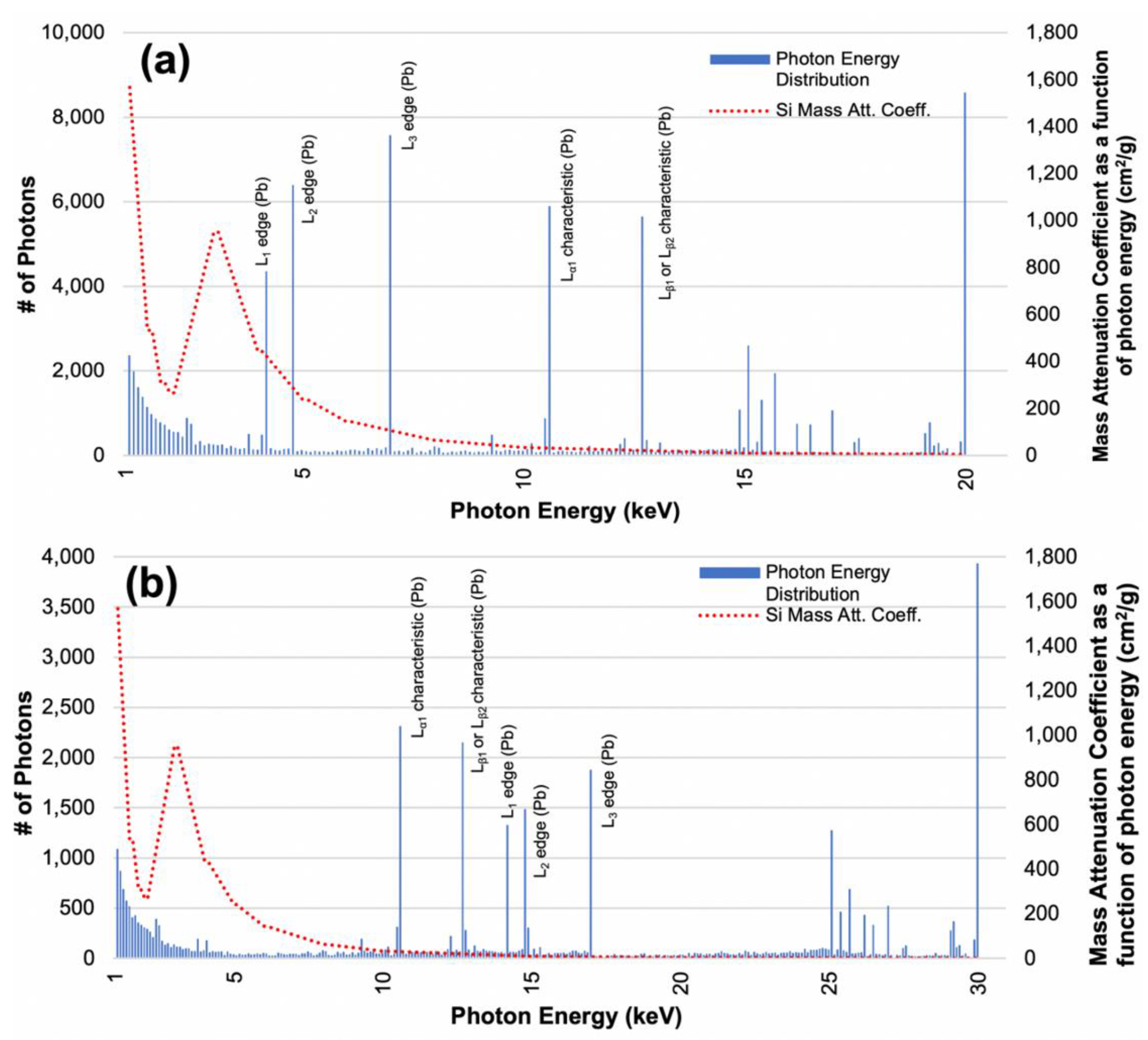
3.1. Verification of Photon Energy Attenuation in High-Z PAL

To verify the concept of photon energy attenuation in thin-film PAL using high-Z semiconductor materials, energy distributions of the photons transmitted through the high-Z PAL have been modeled with MCNP6.2. The MCNP simulation was conducted on 105 incident photons, and the transmitted photon energy histograms are plotted in 0.1 keV bins. We confirm that the transmitted photons have a much lower energy than the incident ones, and a notable fraction will have energies <10 keV to facilitate absorption by Si as shown in Figure 2a,b for 20 and 30 keV incident X-ray photons after transmitting through a 1 μm PbTe PAL, respectively, both using 50 µm pixel size. These figures do not show the energy range of 0–1 keV since there is a default artificial photon energy cutoff around 1 keV in our MCNP simulation and important effects for scattering leading to lower energies are not yet included in MCNP6.2 photon transport methods, resulting in photon energies below the cutoff to not be calculated [45,46]. This cutoff tends to underestimate the photon absorption in Si because the mass attenuation coefficients of Si decrease with photon energy, as shown in Figure 2a,b to demonstrate overlaps with the down-converted X-ray photon spectra [13,47]. From Figure 2, we find that the photon energies are down-converted mainly into two distinctive regimes after transmitting through 1 μm-thick PbTe PAL:
(1)
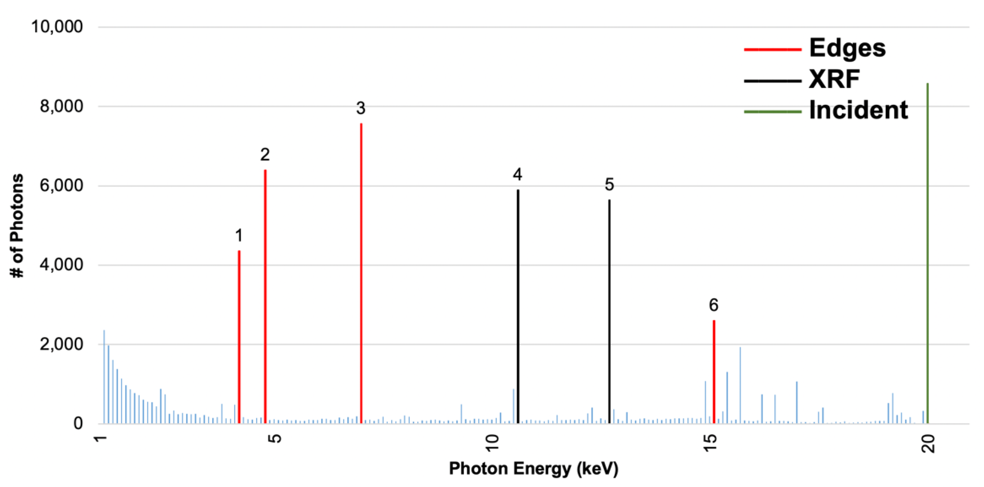
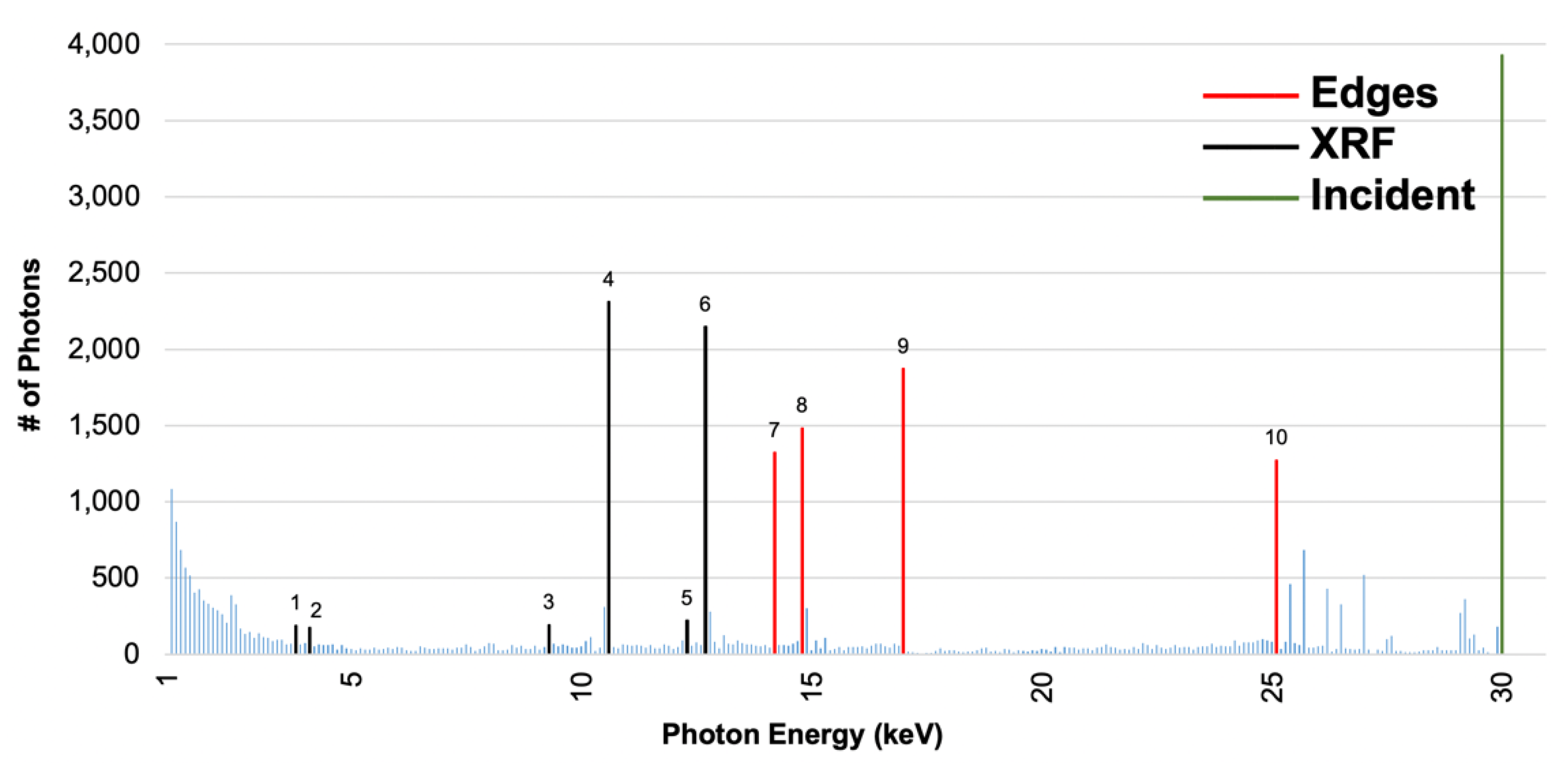
A nearly continuous low energy spectrum at 1–5 keV, where Si has large mass attenuation coefficients for efficient absorption. This regime is induced by multiple inelastic scattering of incident photons;
(2)
Sharp and discrete energy peaks corresponding either to the characteristic X-ray emissions of Pb or Te atoms [48,49,50], or transition energies corresponding to energy losses from incident energies, otherwise known as edges. The characteristic X-ray emissions of Pb or Te atoms also correspond with X-ray fluorescence (XRF) spectrum of Pb and Te [50,51]. Full tables that list the origins of a majority of the significant peaks are provided in Appendix A and Appendix B. This regime is induced by photons that have only experienced from one to a few inelastic scattering events.
For the case of 20 keV incident photons, several major peaks in regime (2) are still located at <10 keV, which can be effectively absorbed by Si. Therefore, both regimes (1) and (2) contribute significantly to enhanced X-ray absorption in Si in this case. As the incident photon energy increases above 30 keV, most of these characteristic X-ray peaks are located at >10 keV (Figure 2b), and efficient absorption of down-converted photons at 1–5 keV in regime (1) become the dominant mechanism of QY enhancement for Si detectors.
Appendix C includes two photon transmissivity (%T) vs. incident X-ray photon energy plots and compare %T calculated using Beer’s Law and %T determined using MCNP without boundary limits for 200 µm-thick Si and 1 µm PbTe. It can be clearly seen that for the case of 200 µm Si, %T calculated using Beer’s Law and MCNP are very similar due to Si being low-Z and does not greatly contribute to photon energy down conversion via inelastic scattering, while for the case of 1 µm PbTe, the theoretical and simulated values demonstrate fairly large discrepancies at lower incident energies. At lower energies, an increased amount of inelastic scattering events results in more photon energy down conversion in PbTe, a high-Z material, causing it to absorb the lower-energy down-converted photons and leading to less transmission of photons. As the incident energy increases, the amount of inelastic scattering events will decrease, allowing simulated %T to be closer to the theoretical Beer’s Law values and closing the gap between the discrepancies.

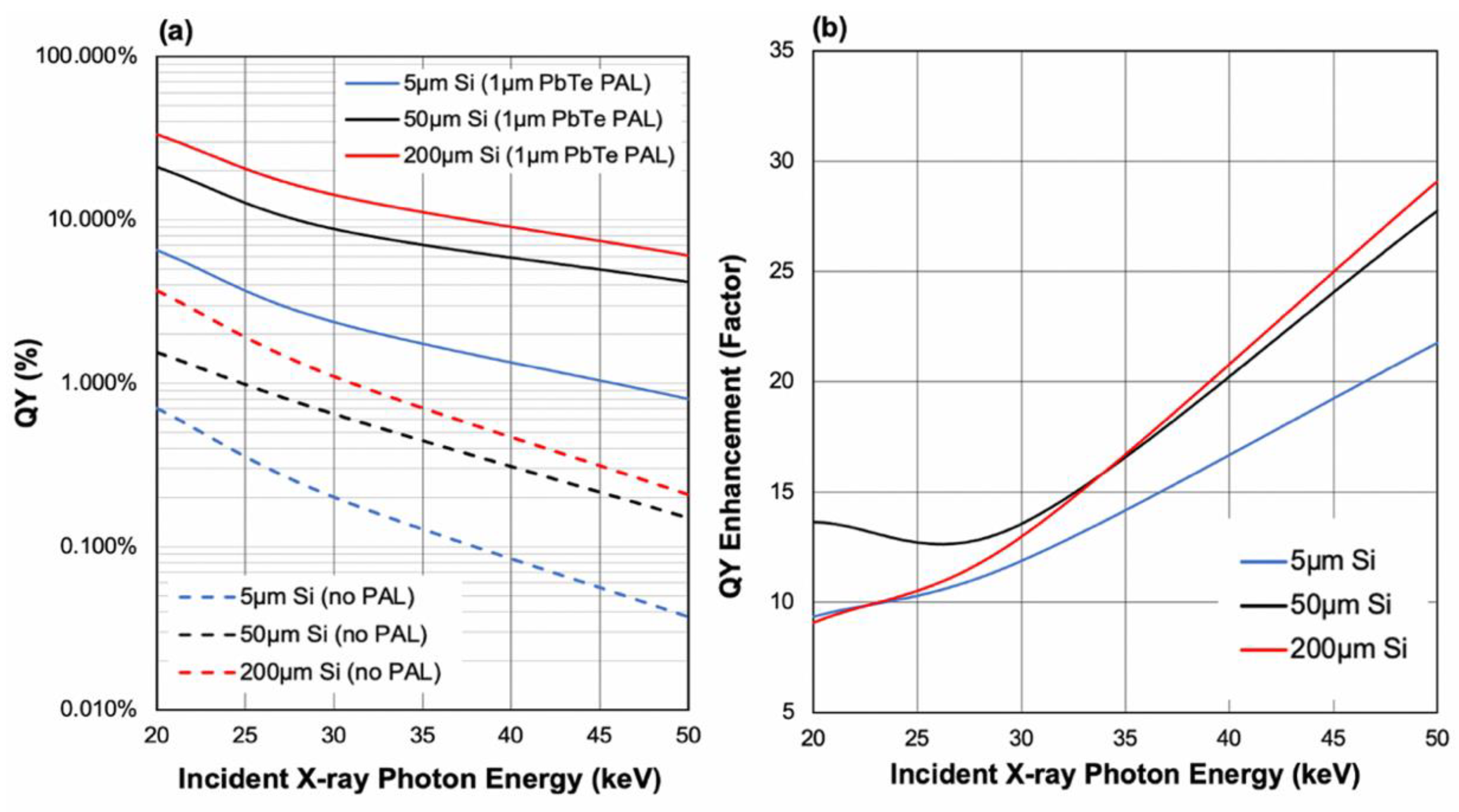
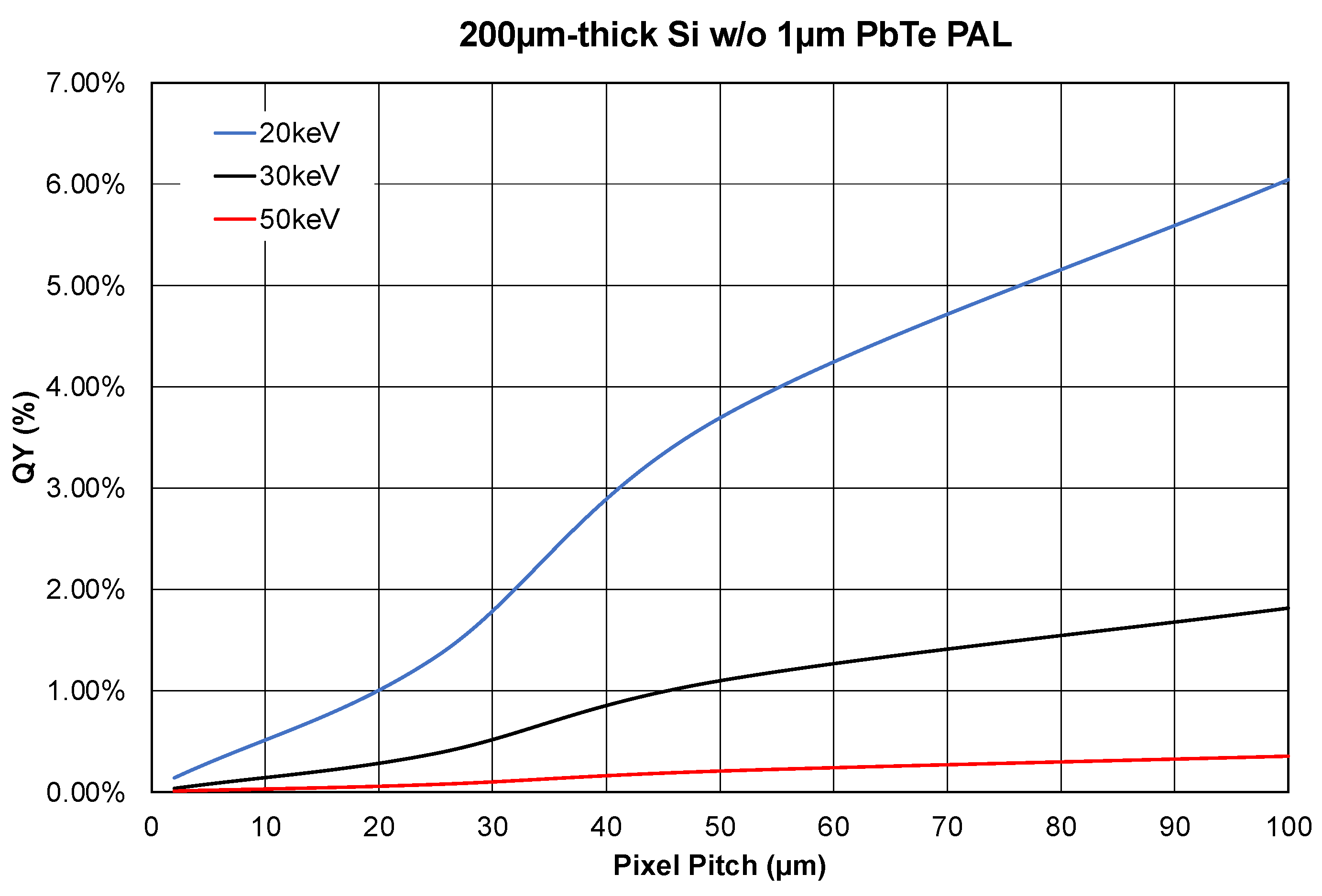
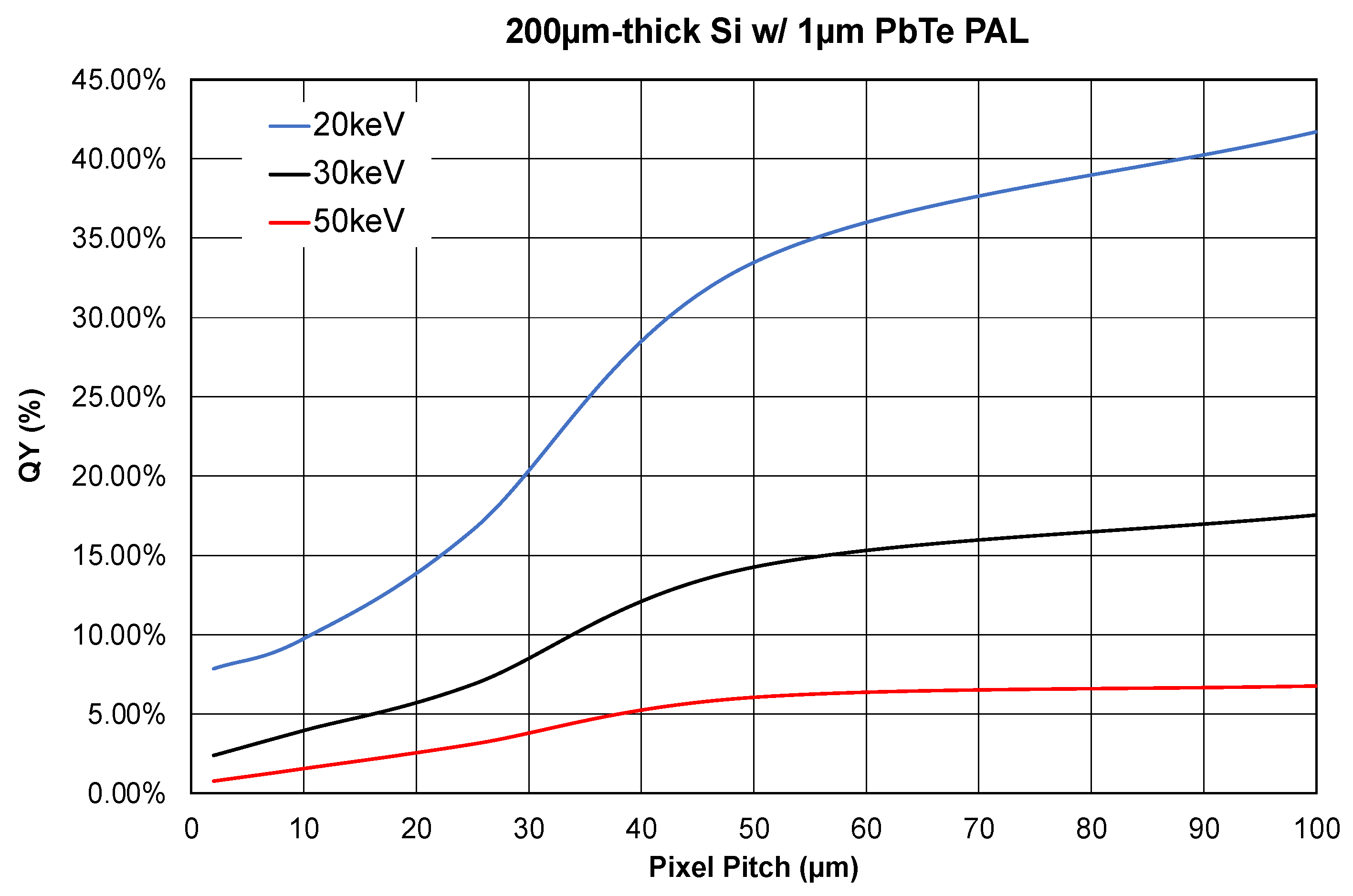
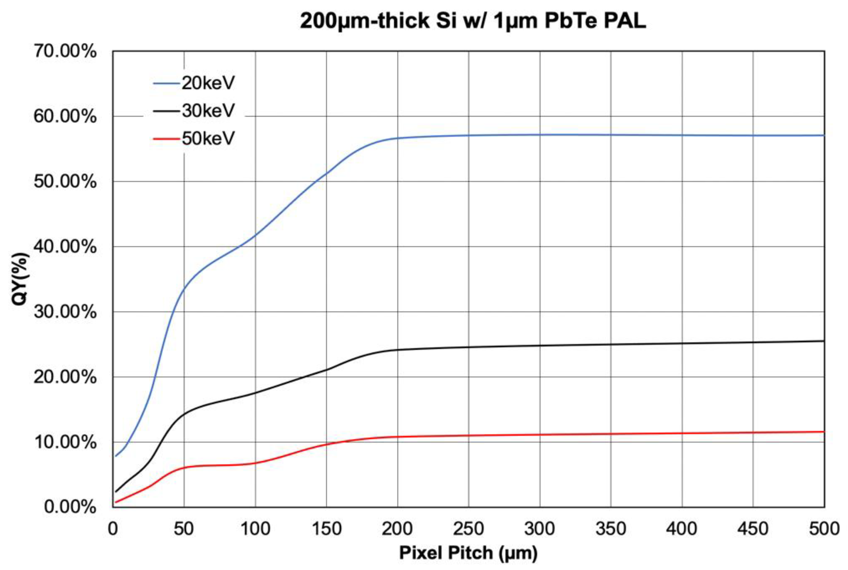
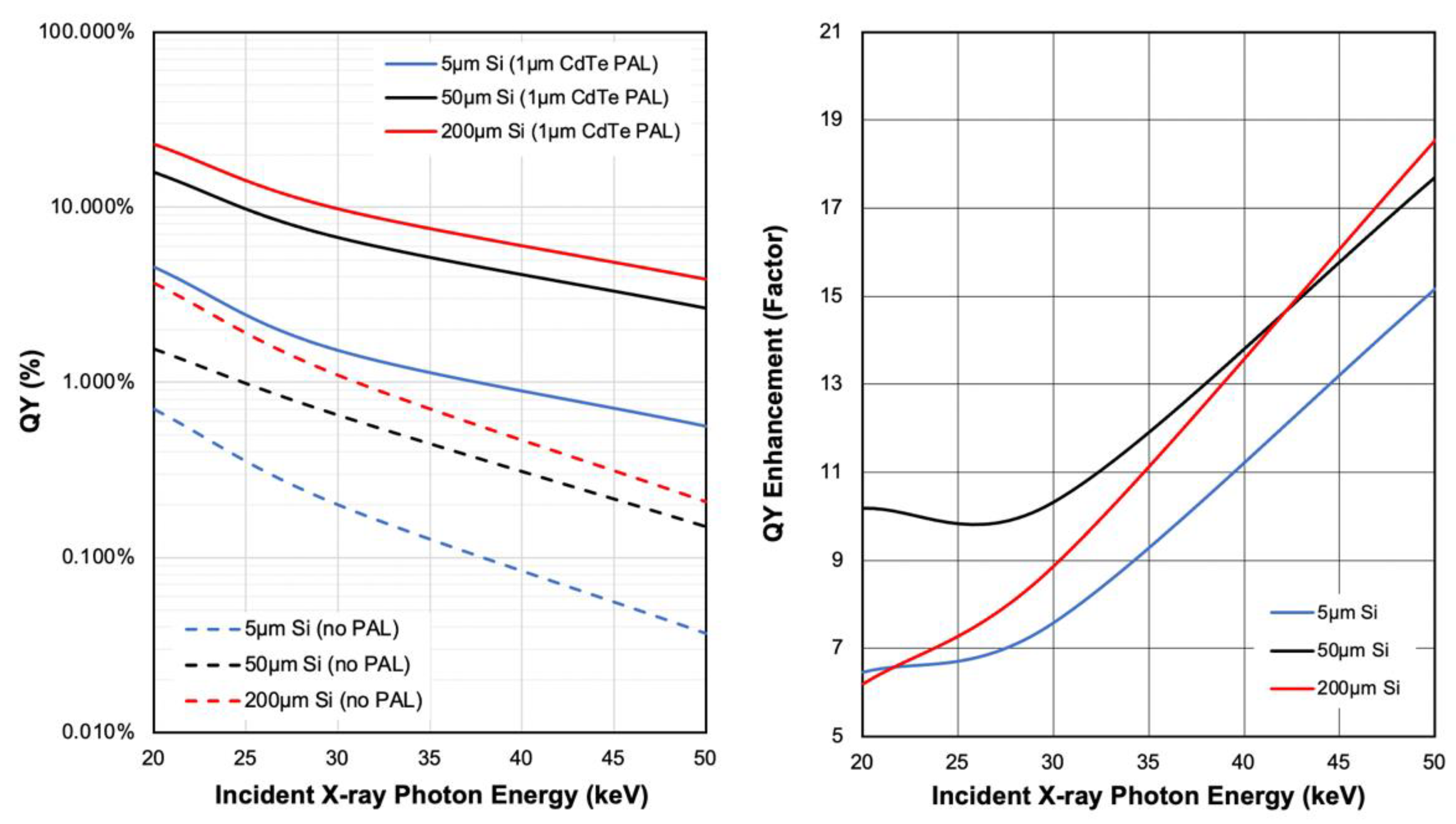
3.2. Quantum Yield Enhancement in Si

Further including 5 μm, 50 μm, and 200 μm-thick Si layers in the MCNP simulation with 105 incident photons, Figure 3a,b compare the QY of Si hard X-ray detectors with and without PAL as a function of incident photon energy based on the definition in Equation (1). The CIS pixel size is 50 × 50 μm2 in the simulation, and the X-ray photons scattered outside the pixel region is no longer tracked/counted. Figure 3a,b demonstrate that incorporating a 1 μm-thick PAL layer can effectively increase the QY of Si detectors by 10–30× depending on the incident photon energy and the Si thickness. Even though the mass attenuation coefficient of Si decreases with photon energy (Figure 2), Figure 3b shows that the QY enhancement contributed by PbTe PAL actually increases with the incident X-ray photon energy. In other words, devices with PAL show much less QY degradation at higher X-ray photon energies. This feature is especially helpful for high-energy X-ray detection. For 5 μm, 50 μm, and 200 μm Si, the QY with 1 µm PbTe PAL (solid lines) ranges between 6.54% and 33.48% for 20 keV photons. Remarkably, even the thinnest 5 µm Si with PAL demonstrates ~2× higher QY than the thickest 200 µm Si without PAL. Furthermore, QYs with PALs are all higher than the ~5% QY at 7.5 keV incident X-ray photon energy, as demonstrated by state-of-the-art photoemission X-ray detectors [17].
With 200 µm-thick Si, it can be seen from Appendix D and Appendix E that <50 µm pixel pitches can lead to a quick roll-off of QY with 1 µm PbTe PAL because the incident X-ray photon is scattered outside the original pixel region, which can indicate a significant crosstalk at <50 µm pixel pitches. In Appendix F, a plot representing the number of exiting photons from 1 µm PbTe PAL vs. pixel pitch can be seen. This confirms that at <50 µm pixel sizes, a significant amount of photons would already be prematurely scattered outside of the original pixel region even prior to reaching the Si layer, leading to the aforementioned indication of significant crosstalk for <50 µm pixels and the quick roll-off of QY. In Appendix E, both plots exhibit two distinctive kinks in QY vs. pixel pitch at 50 µm and 150 µm pixels. The kink shown on 150 µm pixel is caused by the limited lateral scattering distance for X-ray absorption and primary photoelectron excitation at smaller pixels, and the kink shown on 50 µm pixel is due to the crosstalk at <50 µm pixels (i.e., the incident X-ray photon is scattered outside the original pixel after a limited number of scattering events). Furthermore, by comparison, using 200 µm-thick Si without 1 µm PbTe PAL, it can be seen from Appendix D and Appendix E the magnitude of QY decreases much faster with the decrease in pixel size than in the case of having the PAL layer. In fact, without the PAL layer, the QY already almost decreases by half as the pixel size shrinks from 100 µm to 50 μm pixel, in contrast to a less than 15% decrease for the case with PAL. This result indicates that the PAL layer not only helps to drastically enhance the QY, but also helps to reduce the crosstalk by confining the incident X-ray photons and photoelectrons within the original pixel because the X-ray photon energy is down-converted more efficiently. Therefore, there will be a much higher QY especially for ≥50 µm pixel sizes and less limitation in the spatial resolution of direct detection. In addition, there could be lateral scattering of X-ray photons and the generation of primary photoelectrons, especially in larger pixels; therefore, higher efficiency would be seen with larger pixels. As a result, the proposed concept and design would be the most suitable for pixel sizes ≥50 µm. QY will eventually saturate at significantly larger pixels with or without 1 µm PbTe PAL as shown in Appendix C and Appendix D, with the plot with the case of using 1 µm PbTe PAL in Appendix D still showing 3–10× high QY at >200 μm pixel sizes.
Furthermore, while the proposed concept focuses on 1 µm PbTe PAL due to the easiness of material fabrication compared to CdTe, CdTe should also be discussed as it is a common material used in high-energy X-ray photon detection, as previously mentioned. Moreover, 1 µm CdTe PAL is also effective and can provide another option for PAL material. The QY plot for 1 µm CdTe PAL, 50 × 50 μm2 pixel size, and 5 μm, 50 μm, and 200 μm Si can be seen in Appendix G. It is clear that 1 µm CdTe PAL results in less QY than 1 µm PbTe PAL, which is expected due to Cd being lower-Z than Pb, resulting in less inelastic scattering events, but it still provides 6–19x QY enhancement from the case of having no PAL.

3.3. Impact Ionization Process

The average energies corresponding to the primary photoelectrons in Si from Figure 3a solid lines are found to be in the keV range; therefore, impact ionization processes due to regenerative actions should take place. As previously stated, impact ionization processes to promote electrons in the valence band to the conduction band can further provide significant increase to the number of lower-energy electrons that will be generated within Si. The number of primary photoelectrons upon X-ray excitation associated with the QY and the approximate total # of electrons after impact ionization are shown in Table 1. To approximate the number of electrons post-impact ionization processes, the following equation can be taken into consideration:
#   o f   e l e c t r o n s   i n   S i   a f t e r   i m p a c t   i o n i z a t i o n = a v g .   p r i m a r y   p h o t o e l e c t r o n   e n e r g y   i n   S i   [ e V ] × #   o f p r i m a r y   p h o t o e l e c t r o n s   i n   S i   E G L 3.65 e V E H P ,
In Equation (3), the average energies and the number of the primary photoelectrons generated in Si prior to additional impact ionization processes can be determined using MCNP6.2 for devices with 1 μm PbTe PAL (i.e., corresponding to the solid lines in Figure 3a). The product of these two should be divided by 3.65 eV, the aforementioned average energy required to generate an EHP in Si [3,24,25,26], to approximate the ultimate total number of electrons in Si after impact ionization. Table 1 shows the comparison between the number of X-ray excited primary photoelectrons before impact ionization (which were used to determine the QY in Figure 3a) and the approximate number of electrons post-impact ionization using Equation (3). All cases lead to an approximate regenerative increase in lower-energy electrons by a factor of 103–104.

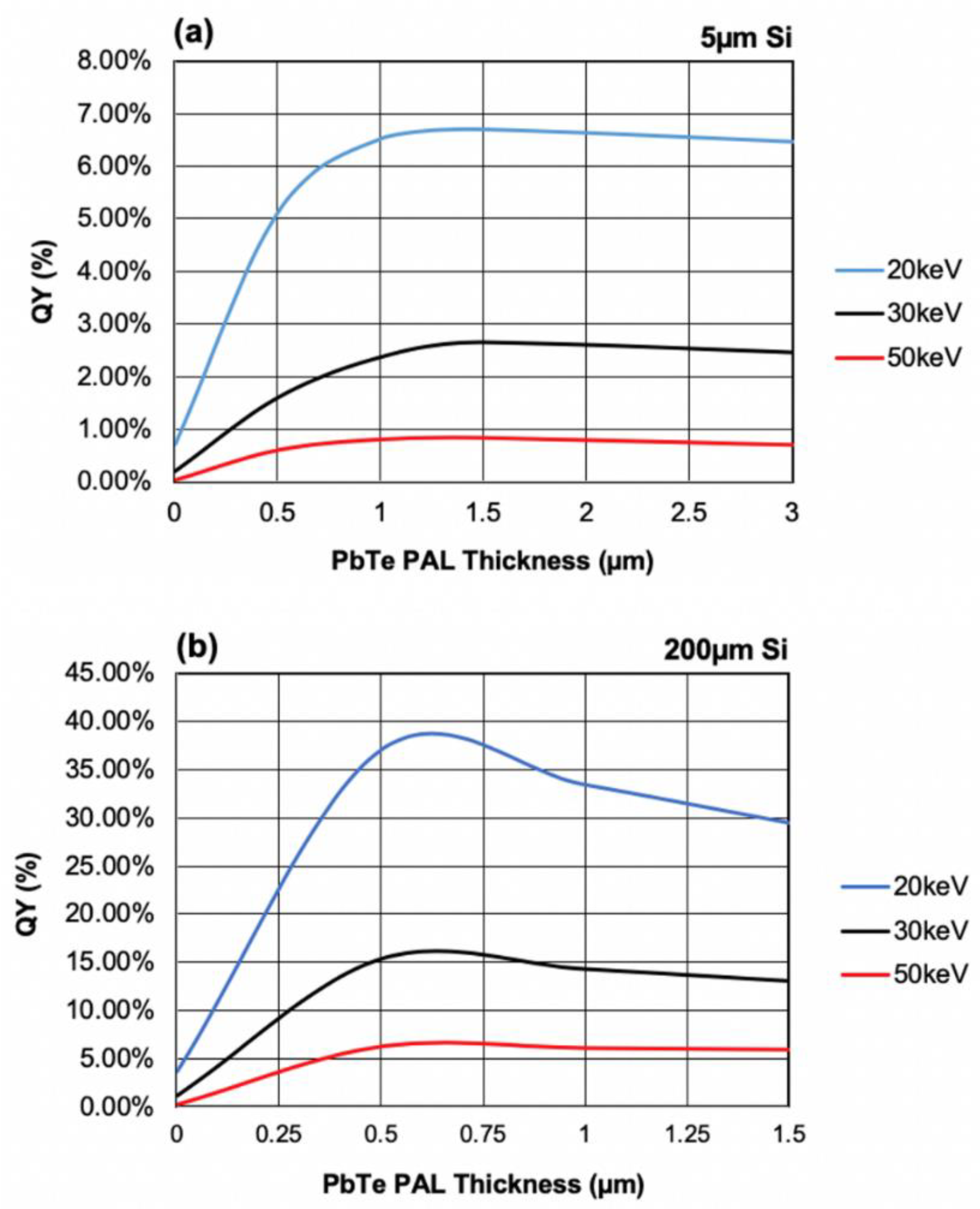
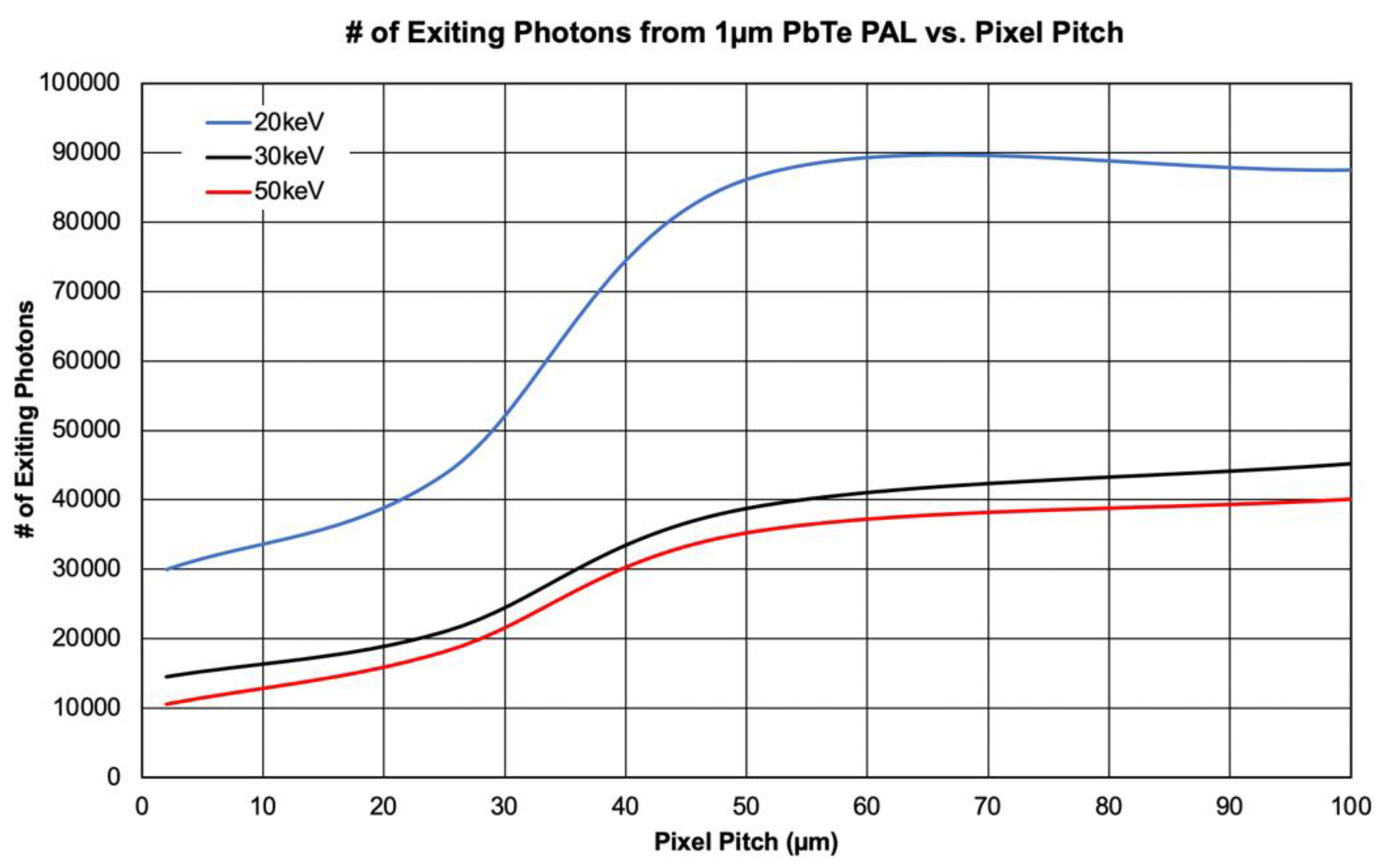
3.4. PAL Thickness Optimization

It was previously mentioned that optimal thicknesses of PAL corresponding to incident X-ray photon energies and Si thicknesses can be determined. To confirm this statement, different thicknesses of PbTe PAL were placed on top of 5 μm and 200 μm Si at 20 keV, 30 keV, and 50 keV incident X-ray photon energies and 50 µm pixel to demonstrate that PAL thicknesses can be optimized according to different incident energies and Si thicknesses. In Figure 4a, with 5 μm Si and the three different incident energies, a peak between 1 μm and 1.5 μm PbTe PAL is seen, indicating that 1 μm–1.5 μm PbTe PAL will result in highest QY with 5 μm Si at the corresponding incident energies. In Figure 4b, with 200 μm Si and the three different incident energies, a peak between 0.5 μm and 0.75 μm PbTe PAL is seen; therefore, 0.5 μm–0.75 μm PbTe PAL will result in the highest QY with 200 μm Si. Notably, a QY approaching 40% can be achieved for 20 keV incident photons, and 16% for 35 keV incident photons. These results further confirm the potentials of PAL layers for integration with Si-based high-energy X-ray detectors.

4. Concluding Remarks

In this article, we introduced a new high-energy X-ray direct detection concept capable of enhancing the QY by 10–30× for Si-based X-ray detectors using high-Z PAL, with a great potential to well surpass the performance of state-of-the-art X-ray detectors based on Si CCD or photocathodes and well-established scintillation- and CdTe-based methods. There have been recent significant efforts to increase the total efficiency of scintillation-based methods, but the enhancements observed so far have been unremarkable and the total efficiency still remains low due to the light extraction efficiency being limited by total internal reflection. The proposed concept may also have the capabilities to be optimized and applied to CdTe-based photodetectors to reduce the required thicknesses as the current state-of-the-art CdTe-based methods require considerably thick layers of the material, which will limit the response time of the devices. This simple yet highly effective device structure and its underlying principle of X-ray photon energy down-conversion have the potential to transform X-ray detection, e.g., spatial resolution and response time. Additional schemes of PAL and EGL layer material choices and optimizations are possible as the overall innovation of the proposed concept is the integration of PAL with EGL, while the PAL can be other adequate high-Z materials not necessarily limited to semiconductors and the EGL can be Si, CdTe, or other adequate semiconductor materials. It should also be noted that with the PAL-EGL concept, the potential exploitation of the photons with incident energies as well as the incoming energy-attenuated photons from the PAL to the EGL may be viable. The former would rely on the choices of materials and their thicknesses. The latter can be readily inferred from the number of photo-electrons in the EGL after impact ionization. To further determine the original incident photon energy, one could potentially utilize the differences in attenuated photon energy distribution shown in Figure 2. For example, 20 keV incident photons have a substantial probability of being attenuated to 4–10 keV, yet 30 keV incident photons have little probability to fall into this energy range after being attenuated by the PbTe PAL layer. Based on this kind of input, data-driven approaches such as machine learning, deep learning, and artificial intelligence that are often used for medical imaging applications, especially those that use scintillation crystals, could be trained/applied to determine the most probable incident photon energy before passing through PAL [52,53]. Furthermore, with the capability of monolithic integration with Si CIS, the PAL-enhanced image sensors can also pave the way towards a wide field-of-view X-ray camera designs for synchrotron and X-ray free electron laser light source applications [3,4]. The modeling in this work will guide future experimental verification towards high-resolution, high-efficiency X-ray detection using PAL-enhanced Si CIS and as a strong candidate to be utilized in the future advancements of X-ray camera designs crucial for synchrotron and X-ray free electron laser light source applications.

Author Contributions

PAL modeling work was performed by E.L. under the supervisions of J.L. and Z.W. and work pertinent to photon energy distribution and impact ionization were contributed by K.M.A. and E.R.F. M.R.J. provided guidance for initial simulation work. The manuscript was prepared by E.L. under the guidance of J.L. All authors have read and agreed to the published version of the manuscript.

Funding

This research was supported by the Experimental Science Program (C3) at Los Alamos National Laboratory under the subcontract number 537679 and basic agreement number 537992 with The Trustees of Dartmouth College. It was also supported by the United States Department of Energy National Nuclear Security Administration Laboratory Residency Graduate Fellowship (DOE NNSA LRGF) under the award numbers DE-NA0003864 and DE-NA0003960. Los Alamos National Laboratory is managed by Triad National Security, LLC for the United States Department of Energy.

Data Availability Statement

Not applicable.

Conflicts of Interest

The authors declare no conflict of interest.

Appendix A

Table of peaks in 0.1 keV bin photon energy distribution plot representing energies corresponding to energy losses from incident energies (edges) or characteristic X-ray energies (XRF): 1 µm PbTe PAL at 20 keV incident energy. Energy losses from incident are the differences between incident energies and peak energies. Peaks corresponding to edges are shown in red and peaks corresponding to XRF are shown in black. The incident energy peak is shown in green. The remaining blue peaks are attenuated photons via inelastic scattering processes. The broadened structures from 15 keV to 18 keV are presumably photons that have not undergone enough inelastic scattering processes in PAL to lose significant energy.
Figure A1. Transmitted photon energy distribution histogram from Figure 2a with the origins of the majority of the significant peaks.
Instruments 05 00017 g0a1
Table A1. List of origins of the significant peaks numbered in Figure A1.
Peak #Peak Energy (keV)Energy Loss from Incident (keV)Transition Corresponding to LossXRF Peak
615.14.9L1 edge (Te) or M (Pb)-
512.77.3-Lβ1 or Lβ2 (Pb)
410.69.4-Lα1 (Pb)
37.013.0L3 edge (Pb)-
24.815.2L2 edge (Pb)-
14.215.8L1 edge (Pb)-

Appendix B

Table of peaks in 0.1 keV bin photon energy distribution plot representing energies corresponding to energy losses from incident energies (edges) or characteristic X-ray energies: 1 µm PbTe PAL at 30 keV incident energy. Energy losses from incident are the differences between incident energies and peak energies. Peaks corresponding to edges are shown in red and peaks corresponding to XRF are shown in black. The incident energy peak is shown in green. The remaining blue peaks are attenuated photons via inelastic scattering processes. The broadened structures from 25 keV to 28 keV are presumably photons that have not undergone enough inelastic scattering processes in PAL to lose significant energy.
Figure A2. Transmitted photon energy distribution histogram from Figure 2b with the origins of the majority of the significant peaks.
Instruments 05 00017 g0a2
Table A2. List of origins of the significant peaks numbered in Figure A2.
Peak #Peak Energy (keV)Energy Loss from Incident (keV)Transition Corresponding to LossXRF Peak
1025.14.9L1 edge (Te) or M (Pb)--
917.013.0L3 edge (Pb)--
814.815.2L2 edge (Pb)--
714.215.8L1 edge (Pb)--
612.717.3--Lβ1 or Lβ2 (Pb)
512.317.7--Lβ4 (Pb)
410.619.4--Lα1 (Pb)
39.320.7--L or L τ (Pb)
24.125.9--Lβ3 (Te)
13.826.2--Lα1 (Te)

Appendix C

%T vs. incident X-ray photon energy for 200 µm Si (left) and 1 µm PbTe (right). %T obtained using theoretical Beer’s Law calculations and Monte Carlo (MC) simulations are similar for 200 µm Si and discrepancies are demonstrated for 1 µm PbTe, especially at lower incident energies. As Si is low-Z, MC will not demonstrate photon energy down conversion via inelastic scattering. However, in 1 µm PbTe, as less inelastic scattering events occur at higher incident energies, the gap between the discrepancies will decrease and the discrepancies will remain relatively large at lower energies due to more inelastic scattering.
Figure A3. %T vs. incident X-ray photon energies for 200 µm Si (left) and 1 µm PbTe (right). %T is calculated using Beer’s Law and MCNP.
Instruments 05 00017 g0a3

Appendix D

QY vs. pixel pitch without (Figure A4) and with (Figure A5) 1 µm PbTe PAL and 200 µm Si thicknesses at 20 keV, 30 keV, and 50 keV incident energies. Pixel sizes were varied from 2 µm to 100 µm. The quick roll-off in QY at 50 µm pixel can indicate a significant crosstalk at <50 µm pixel pitches. As a result, the proposed concept would be the most suitable for ≥50 µm pixels. It can be seen that the magnitude of QY with decreasing pixel is greater in the case of having no 1 µm PbTe PAL.
Figure A4. QY vs. pixel pitch (2–100 µm) without 1 µm PbTe PAL and 200 µm Si at 20 keV, 30 keV, and 50 keV incident X-ray photon energies.
Instruments 05 00017 g0a4
Figure A5. QY vs. pixel pitch (2–100 µm) with 1 µm PbTe PAL and 200 µm Si at 20 keV, 30 keV, and 50 keV incident X-ray photon energies.
Instruments 05 00017 g0a5

Appendix E

QY vs. pixel pitch without (Figure A6) and with (Figure A7) 1 µm PbTe PAL and 200 µm Si thicknesses at 20 keV, 30 keV, and 50 keV incident energies. Pixel sizes were varied from 2 µm to 500 µm. It can be seen that the magnitude of QY with decreasing pixel pitch is greater in the case of having no 1 µm PbTe PAL. At significantly larger pixels, especially beyond 200 µm pixels, the QYs eventually saturate for both cases of with and without 1 µm PbTe PAL.
Figure A6. QY vs. pixel pitch (2–500 µm) without 1 µm PbTe PAL and 200 µm Si at 20 keV, 30 keV, and 50 keV incident X-ray photon energies.
Instruments 05 00017 g0a6
Figure A7. QY vs. pixel pitch (2–500 µm) with 1 µm PbTe PAL and 200 µm Si at 20 keV, 30 keV, and 50 keV incident X-ray photon energies.
Instruments 05 00017 g0a7

Appendix F

Number of Exiting Photons from 1 µm PbTe PAL vs. Pixel Pitch at 20 keV, 30 keV, and 50 keV incident energies. Pixel sizes were varied from 2 µm to 100 µm. It can be seen that at around 50 µm, the number of exiting photons significantly decreases as the pixel size decreases at a much quicker slope, indicating that with <50 µm pixels, considerable amounts of photons are prematurely scattered outside of the original pixel region before reaching the Si layer, resulting in much lower QY and significant crosstalk issues.
Figure A8. # of exiting photons from 1 µm PbTe PAL at 20 keV, 30 keV, and 50 keV incident X-ray photon energies vs. pixel pitch (2–100 µm).
Instruments 05 00017 g0a8

Appendix G

QY vs. incident X-ray photon energy (left) and QY enhancement (factor) vs. incident X-ray photon energy (right) with 1 µm CdTe PAL, 50 × 50 μm2 pixel size, and 5 μm, 50 μm, and 200 μm Si. Using 1 µm CdTe as PAL enhances QY by 6–19x from not having PAL. The enhancement is lower than PbTe PAL, which is expected due to lower-Z of Cd leading to less scattering events.
Figure A9. QY vs. incident photon energy with and without 1 µm CdTe PAL shown with solid and dashed lines, respectively (left) and QY enhancement (factor) vs. incident photon energy for three different Si thicknesses to represent that 1 µm CdTe PAL can increase the QY as opposed to having no PAL (right).
Instruments 05 00017 g0a9

References

  1. Li, X.; Chu, P.; Wang, Z.; O’Shaughnessy, C.M.; Morris, C.; Demarteau, M.; Wagner, R.; Xie, J.; Xia, L.; Zhu, R.-Y.; et al. Initial assessment of multilayer silicon detectors for hard X-ray imaging. Nucl. Instrum. Methods Phys. Res. A 2019, 942, 162414. [Google Scholar] [CrossRef]
  2. Hu, C.; Zhang, L.; Zhu, R.-Y.; Demarteau, M.; Wagner, R.; Xia, L.; Xie, J.; Li, X.; Wang, Z.; Shih, Y.; et al. Ultrafast inorganic scintillator-based front imager for gigahertz hard X-ray imaging. Nucl. Instrum. Methods. Phys. Res. A 2019, 940, 223–229. [Google Scholar] [CrossRef]
  3. Wang, Z. On the Single-Photon-Counting (SPC) modes of imaging using an XFEL source. J. Instrum. 2015, 10, C12013. [Google Scholar] [CrossRef] [Green Version]
  4. Wang, Z.; Barnes, C.W.; Dattelbaum, D.M.; Fossum, E.R.; Lee, E.; Liu, J.; Ma, J.J.; Pokharel, R.; Sechrest, Y.H.; Sweeney, C.M.; et al. Los Alamos National Laboratory Report No. LA-UR-19-27804; Los Alamos National Laboratory: Los Alamos, NM, USA, 2019. [Google Scholar]
  5. Lee, E.; James, M.R.; Wang, Z.; Liu, J. Monte Carlo simulation and design of high-energy X-ray detection concept with enhanced efficiency using high-Z semiconductor photon attenuation materials. OSA Tech. Dig. 2020, NoTu2F.3. [Google Scholar] [CrossRef]
  6. Derenzo, S.E.; Choong, W.; Moses, W.W. Fundamental limits of scintillation detector timing precision. Phys. Med. Biol. 2014, 59, 3261–3286. [Google Scholar] [CrossRef] [PubMed]
  7. Lynch, F.J. Basic limitation of scintillation counters in time measurements. IEEE Trans. Nucl. Sci. 1975, 22, 58–64. [Google Scholar] [CrossRef] [Green Version]
  8. Huber, M.C.E.; Pauluhn, A.; Timothy, J.G. Observing Photons in Space; Springer: New York, NY, USA, 2013; pp. 409–418. [Google Scholar]
  9. X-ray Detectors, Hamamatsu Photonics. Available online: https://www.hamamatsu.com/resources/pdf/ssd/e09_handbook_xray_detectors.pdf (accessed on 23 March 2020).
  10. Parsai, E.I.; Shvydka, D.; Kang, J. Design and optimization of large area thin-film CdTe detector for radiation therapy imaging applications. Med. Phys. 2010, 37, 3980. [Google Scholar] [CrossRef] [PubMed]
  11. Shvydka, D.; Parsai, E.I. Performance of large area thin-film CdTe detector in diagnostic x-ray imaging. Int. J. Med. Phys. Clin. Eng. Radiat. Oncol. 2013, 2, 98–109. [Google Scholar] [CrossRef] [Green Version]
  12. Hondongwa, D.B.; Fossum, E.R. Temporally over sampled CMOS X-ray photon counting sensor for low dose fluoroscopy. In Proceedings of the 2017 IEEE 60th International Midwest Symposium on Circuits and Systems (MWSCAS), Boston, MA, USA, 6–9 August 2017; pp. 1101–1104. [Google Scholar]
  13. Thompson, A.C.; Attwood, D.; Gullikson, E.M.; Howells, M.R.; Kim, K.-J.; Kirz, J.; Kortright, J.B.; Lindau, I.; Liu, Y.; Pianetta, P.; et al. Lawrence Berkeley National Laboratory Report No. LBNL/PUB-490 Rev. 3; Lawrence Berkeley National Laboratory: Berkeley, CA, USA, 2009. [Google Scholar]
  14. Miyai, H.; Kitaguchi, H.; Kawasaki, S.; Izumi, S. Response of silicon detector for high energy X-ray computed tomography. IEEE Trans. Nucl. Sci. 1994, 41, 999–1003. [Google Scholar] [CrossRef]
  15. Nikzad, S.; Cunningham, T.J.; Hoenk, M.E.; Ruiz, R.P.; Soules, D.M.; Holland, S.E. Direct detection of 0.1-20 keV electrons with delta doped, fully depleted, high purity silicon p-i-n diode arrays. Appl. Phys. Lett. 2006, 89, 182114. [Google Scholar] [CrossRef]
  16. Fraser, G.W.; Abbey, A.F.; Holland, A.; McCarthy, K.; Owens, A.; Wells, A. The X-ray energy response of silicon Part A. Theory. Nucl. Instrum. Methods Phys. Res. A 1994, 350, 368–378. [Google Scholar] [CrossRef]
  17. Opachich, Y.P.; Bell, P.M.; Bradley, D.K.; Chen, N.; Feng, J.; Gopal, A.; Hatch, B.; Hilsabeck, T.J.; Huffman, E.; Koch, J.A.; et al. Structured photocathodes for improved high-energy X-ray efficiency in streak cameras. Rev. Sci. Instrum. 2016, 87, 11E331. [Google Scholar] [CrossRef] [PubMed]
  18. Henke, B.; Knauer, J.; Premaratne, K. The characterization of x-ray photocathodes in the 0.1-10-keV photon energy region. J. Appl. Phys. 1981, 52, 1509. [Google Scholar] [CrossRef]
  19. Reinhardt, K.; Kern, W. Handbook of Silicon Wafer Cleaning Technology; William Andrew Publishing: New York, NY, USA, 2018; p. 634. [Google Scholar]
  20. Leitz, C.; Rabe, S.; Prigozhin, I.; Burke, B.; Zhu, M.; Ryu, K.; Cooper, M.; Reich, R.; Johnson, K.; Hu, W.; et al. Germanium CCDs for large-format SWIR and X-ray imaging. J. Instrum. 2017, 12, C05014. [Google Scholar] [CrossRef]
  21. Rumaiz, A.; Kuczewski, A.; Mead, J.; Vernon, E.; Pinelli, D.; Dooryhee, E.; Ghose, S.; Caswell, T.; Siddons, D.; Miceli, A.; et al. Multi-element germanium detectors for synchrotron applications. J. Instrum. 2018, 13, C04030. [Google Scholar] [CrossRef] [Green Version]
  22. Veale, M.C.; Bell, S.J.; Duarte, D.D.; French, M.J.; Schneider, A.; Seller, P.; Wilson, M.D.; Lozinskaya, A.D.; Novikov, V.A.; Tolbanov, O.P.; et al. Chromium compensated gallium arsenide detectors for X-ray and gamma-ray spectroscopic imaging, Nuc. Instrum. Methods Phys. Res. A 2014, 752, 6–14. [Google Scholar]
  23. Miyajima, S. Thin CdTe detector in diagnostic X-ray spectroscopy. Med Phys. 2003, 30, 771–777. [Google Scholar] [CrossRef]
  24. Amsterdam Scientific Instruments. LynX Hybrid Pixel Detectors for X-ray. 2017. Available online: https://www.amscins.com/products/lynx/ (accessed on 18 March 2021).
  25. Brient, J.-C.; Rusack, R.; Sefkow, F. Silicon calorimeters. Ann. Rev. Nucl. Part. Sci. 2018, 68, 271–290. [Google Scholar] [CrossRef]
  26. Compagnie de Saint-Gobain, S.A. Efficiency Calculations for Selected Scintillators. Available online: https://www.crystals.saint-gobain.com/sites/imdf.crystals.com/files/documents/efficiency-calculations.pdf (accessed on 18 March 2021).
  27. Compagnie de Saint-Gobain, S.A. NaI(TI) and Polyscin NaI(TI) Sodium Iodide Scintillation Material. Compagnie de Saint-Gobain, S.A. Available online: https://www.crystals.saint-gobain.com/sites/imdf.crystals.com/files/documents/sodium-iodide-material-data-sheet_0.pdf (accessed on 18 March 2021).
  28. Chen, X.; Liu, B.; Zhu, J.; Gu, M.; Chen, H.; Liu, J.; Chen, L.; Ouyang, X. Light extraction enhancement and directional control of scintillator by using microlens arrays. Opt. Express 2018, 26, 23132–23141. [Google Scholar] [CrossRef]
  29. Wang, Z.; Morris, C.; Kapustinsky, J.S.; Kwiatkowski, K.; Luo, S.-N. Towards hard X-ray imaging at GHz frame rate. Rev. Sci. Instrum. 2012, 83, 10E510. [Google Scholar] [CrossRef] [Green Version]
  30. Hubbell, J.H.; Grimm, H.A.; Overbo, I. Pair, triplet, and total atomic cross sections (and mass attenuation coefficients) for 1 MeV–100 GeV photons in elements Z = 1 to 100. J. Phys. Chem. Ref. Data 1980, 9, 1023–1148. [Google Scholar] [CrossRef]
  31. Gierga, D.P. Electron Photon Calculations Using MCNP. Ph.D. Thesis, Massachusetts Institute of Technology, Cambridge, MA, USA, 1998. [Google Scholar]
  32. Durini, D. High Performance Silicon Imaging: Fundamentals and Applications of CMOS and CCD Sensors; William Andrew Publishing: Cambridge, UK, 2019; p. 476. [Google Scholar]
  33. Lutz, G. Silicon drift and pixel devices for X-ray imaging and spectroscopy. J. Synchrotron Radiat. 2006, 13, 2. [Google Scholar] [CrossRef] [PubMed]
  34. Kitchin, C.R. Astrophysical Techniques; CRC Press: Boca Raton, FL, USA, 2013; p. 159. [Google Scholar]
  35. Ismail, M.P.b.; Ssni, S.b.; Masenwat, N.A.b.; Mohd, S.; Sayuti, S.; Ahmad, M.R.B.; Mahud, M.H.b.; Isa, N.b. Radiation attenuation on labyrinth design bunker using Iridium-192 source. AIP Conf. Proc. 2017, 1799, 050011. [Google Scholar]
  36. Owens, A. Semiconductor Radiation Detectors; CRC Press: Boca Raton, FL, USA, 2019. [Google Scholar]
  37. Singh, V.K.; Lin, P.T.; Patel, N.; Lin, H.; Li, L.; Zou, Y.; Deng, F.; Ni, C.; Hu, J.; Giammarco, J.; et al. Mid-infrared materials and devices on a Si platform for optical sensing. Sci. Technol. Adv. Mater. 2014, 15, 014603. [Google Scholar] [CrossRef]
  38. Piccioni, G.; Formisano, V.; Bellucci, G. Evaluation of aPbTe detector for infrared imaging purposes. Nuovo Cimento C 1992, 15, 1121–1128. [Google Scholar] [CrossRef]
  39. Corsi, C. PbTe rf-sputtered infrared detectors. Appl. Phys. Lett. 1974, 24, 137. [Google Scholar] [CrossRef]
  40. Schulman, T. Si, CdTe, and CdZnTe Radiation Detectors for Imaging Applications. Ph.D. Thesis, University of Helsinki, Helsinki, Finland, 2006. [Google Scholar]
  41. Piccioni, G.; Formisano, V.; Bellucci, G. Polarization of Bi2Te3 thin film in a floating-gate capacitor structure. Appl. Phys. Lett. 2014, 105, 233505. [Google Scholar]
  42. Lin, P.T.; Singh, V.; Wang, J.; Lin, H.; Hu, J.; Richardson, K.; Musgraves, J.D.; Luzinov, I.; Hensley, J.M.; Kimerling, L.C.; et al. Si-CMOS compatible materials and devices for mid-IR microphotonics. Opt. Mater. Express 2013, 3, 1474–1487. [Google Scholar] [CrossRef]
  43. Del Sordo, S.; Abbene, L.; Caroli, E.; Mancini, A.M.; Zappettini, A.; Ubertini, P. Progress in the Development of CdTe and CdZnTe Semiconductor Radiation Detectors for Astrophysical and Medical Applications. Sensors 2009, 9, 3491–3526. [Google Scholar] [CrossRef] [PubMed]
  44. Islamian, J.P.; Abbaspour, S.; Mahmoudian, B. Cadmium telluride semiconductor detector for improved spatial and energy resolution radioisotopic imaging. World J. Nucl. Med. 2017, 16, 101–107. [Google Scholar] [CrossRef] [PubMed]
  45. Yoriyaz, H.; Moralles, M.; Siqueira, P.d.T.D.; Guimaeaes, C.d.C.; Cintra, F.B.; Santos, A.d. Physical models, cross sections, and numerical approximations used in MCNP and GEANT4 Monte Carlo codes for photon and electron absorbed fraction calculation. Med. Phys. 2009, 36, 11. [Google Scholar] [CrossRef] [PubMed] [Green Version]
  46. Werner, C.J. Los Alamos National Laboratory Report No. LA-UR-17-29981; Los Alamos National Laboratory: Los Alamos, NM, USA, 2017. [Google Scholar]
  47. Hubbell, J.H.; Seltzer, S.M. National Institute of Standards and Technology Standard Reference Database 126. Available online: https://www.nist.gov/pml/x-ray-mass-attenuation-coefficients (accessed on 2 April 2020).
  48. Berhardt, L.V. Advances in Medicine and Biology; Nova Science Publishers: New York, NY, USA, 2019; pp. 2–44. [Google Scholar]
  49. Deslattes, R.D.; Kessler, E.G., Jr.; Indelocato, P.; de Billy, L.; Anton, J.; Coursey, J.S.; Schwab, D.J.; Chang, J.; Sukumar, R.; Olsen, K.; et al. National Institute of Standards and Technology Standard Reference Database 128. Available online: https://www.nist.gov/pml/x-ray-transition-energies-database (accessed on 2 April 2020).
  50. Ahmed, T. IUPAC vs. Siegbahn Notation of X-ray Transitions. 2014. Available online: https://figshare.com/articles/dataset/IUPAC_vs_Siegbahn_notation_of_x_ray_transitions/1168938 (accessed on 2 April 2020).
  51. XRF Research, Inc. XRF Spectra. Available online: http://www.xrfresearch.com/xrf-spectra/ (accessed on 18 March 2021).
  52. Gong, K.; Berg, E.; Cherry, S.R.; Qi, J. Machine Learning in PET: From Photon Detection to Quantitative Image Reconstruction. Proc. IEEE 2020, 108, 51–68. [Google Scholar] [CrossRef]
  53. Arabi, H.; Zaidi, H. Applications of artificial intelligence and deep learning in molecular imaging and radiotherapy. Eur. J. Hybrid Imaging 2020, 4, 1–23. [Google Scholar] [CrossRef]
Figure 1. (a) Schematics showing the mechanism of high-Z PAL-Si EGL detector design. High-energy X-ray photons (shown with blue arrows) are incident to the top of the high-Z PAL. Incident photons are down-converted (i.e., redshifted, as shown with red arrows) via inelastic scattering in the high-Z PAL and undergo efficient photoelectric absorption by Si; (b) representation of the expected cross-section of backside illuminated CIS- or QIS-based device with PAL-EGL integration; 1 is high-Z PAL, 2 is a thin (<100 nm) backside passivation oxide (e.g., SiO2) that can be added between PAL and Si for practicality but the overall QY should not be affected because down-converted X-ray photons can readily penetrate through the oxide layer, 3 is optional implants or epitaxial growth for surface pinning, 4 are pixelated carrier storage wells, and 5 is front side pixel readout circuitry.
Instruments 05 00017 g001
Figure 2. X-ray photon energy distribution histograms after transmitting through a 50 µm pixel size and 1 μm-thick PbTe PAL layer for (a) 20 keV and (b) 30 keV incident photons. The total number of incident photons is 105, and the histograms are plotted using 0.1 keV energy bins. Each significant discrete peak in the histogram is identified/labeled with either characteristic X-ray emission of Pb/Te atoms (XRF), or incident photon energy subtracted by the energy losses from the absorption edges of Pb/Te. Mass attenuation coefficients of Si as a function of photon energy are also shown in both plots. This mass attenuation coefficient spectrum indicates that X-ray photon energies need to be attenuated below 10 keV for efficient absorption by Si.
Instruments 05 00017 g002
Figure 3. (a) QY in Si as a function of incident photon energy with 1 µm PbTe PAL (solid lines) and without 1 μm PbTe PAL (dashed lines) and with 5 μm, 50 μm, and 200 μm Si and 50 µm pixel; (b) QY enhancement (factor) vs. incident photon energy for the three different Si thicknesses to represent that 1 µm PbTe PAL can remarkably increase the QY as opposed to having no PAL.
Instruments 05 00017 g003
Figure 4. QY of (a) 5 μm Si and (b) Si with different thicknesses of PbTe PAL at 20 keV, 30 keV, and 50 keV incident X-ray photon energies and 50 µm pixel. Optimal PbTe PAL thickness is seen between 1 μm and 1.5 μm for 5 µm Si, and between 0.5 μm and 0.75 μm for 200 μm Si.
Instruments 05 00017 g004
Table 1. Comparison between the number of photoelectrons (before impact ionization) per 105 incident X-ray photons and ultimate # of electrons after impact ionization in 5 μm, 50 μm, and 200 μm Si with 1 μm PbTe PAL and 50 µm pixel. Average electron energies in Si are still in the keV; therefore, further impact ionization processes can be undergone to provide at least three orders of magnitude increase in the # of lower-energy electrons as shown on the far-right column of the table. As expected, thicker Si leads to higher number of electrons.
IncidentEnergy (keV)Si Thickness (µm)Avg. Electron
Energy in Si (keV)
# of Primary Photoelectrons
Pre-Impact Ionization
(Figure 3a Solid Lines)
Approx. Ultimate # of Electrons Post-
Impact Ionization
2054.8365358.65 × 106
3056.7923734.41 × 106
50511.008052.43 × 106
20504.3921,1232.54 × 107
30505.7587991.39 × 107
50508.4541629.64 × 106
202004.2433,4783.89 × 107
302005.4314,2602.12 × 107
502007.7361561.30 × 107
Publisher’s Note: MDPI stays neutral with regard to jurisdictional claims in published maps and institutional affiliations.

