Author Contributions
Conceptualization, A.B.-F., S.B., D.B., L.C., P.D., J.H., A.K. (Asher Kaboth), J.M., R.N., J.N., R.S., N.S., Y.S. and M.O.W.; Data curation, A.D. (Alexander Deisting), A.V.W., E.A., D.B., Z.C.-W., L.C., A.D. (Adriana Dias), P.D., J.H., P.H.-B., S.J., A.K. (Asher Kaboth), A.K. (Alexander Korzenev), M.M., J.M., R.N., T.N., J.N., W.P., H.R.-Y., S.R., A.T., M.U., S.V., M.W. and M.O.W.; Formal analysis, A.D. (Alexander Deisting), A.V.W., E.A., D.B., Z.C.-W., A.D. (Adriana Dias), P.D., J.H., P.H.-B., S.J., M.M., T.N., W.P., H.R.-Y., A.T. and M.W.; Funding acquisition, G.B., A.B.-F., S.B., A.K. (Asher Kaboth), J.M., R.N., J.N., S.R., R.S. and M.O.W.; Investigation, A.D. (Alexander Deisting), A.V.W., E.A., G.B., A.B.-F., C.B., D.B., Z.C.-W., L.C., A.D. (Adriana Dias), P.D., J.H., P.H.-B., S.J., A.K. (Asher Kaboth), A.K. (Alexander Korzenev), W.M., P.M., M.M., J.M., R.N., T.N., J.N., W.P., H.R.-Y., S.R., R.S., N.S., Y.S., J.S., A.T., M.U., S.V., M.W. and M.O.W.; Methodology, A.D. (Alexander Deisting), A.V.W., G.B., A.B.-F., C.B., S.B., D.B., Z.C.-W., L.C., A.D. (Adriana Dias), P.D., J.H., P.H.-B., S.J., A.K. (Asher Kaboth), A.K. (Alexander Korzenev), W.M., P.M., M.M., J.M., R.N., T.N., J.N., W.P., H.R.-Y., S.R., R.S., N.S., Y.S., J.S., A.T., M.U., S.V., M.W. and M.O.W.; Project administration, A.D. (Alexander Deisting), G.B., S.B., L.C., A.K. (Asher Kaboth), J.M., R.N., J.N. and M.O.W.; Resources, S.B., D.B., L.C., A.K. (Asher Kaboth), J.M., R.N., J.N., S.R. and M.O.W.; Software, A.D. (Alexander Deisting), A.V.W., E.A., P.D., J.H., P.H.-B., S.J., T.N., W.P., H.R.-Y., A.T. and S.V.; Supervision, A.D. (Alexander Deisting), A.V.W., G.B., A.B.-F., S.B., L.C., P.D., A.K. (Asher Kaboth), J.M., R.N., J.N., R.S. and M.O.W.; Validation, A.D. (Alexander Deisting), A.V.W., E.A., D.B., Z.C.-W., L.C., P.D., S.J., A.K. (Asher Kaboth), M.M., J.M., R.N., T.N., H.R.-Y. and A.T.; Visualization, A.D. (Alexander Deisting), A.V.W., E.A., Z.C.-W., A.D. (Adriana Dias), P.D., P.H.-B., W.P. and H.R.-Y.; Writing—original draft, A.D. (Alexander Deisting), A.V.W., Z.C.-W., P.D., A.K. (Asher Kaboth), J.M., W.P., H.R.-Y., A.T. and M.O.W.; Writing—review & editing, A.D. (Alexander Deisting), A.V.W., E.A., D.B., Z.C.-W., L.C., A.D. (Adriana Dias), P.D., P.H.-B., A.K. (Asher Kaboth), J.M., J.N., H.R.-Y. and M.O.W. All authors have read and agreed to the published version of the manuscript.
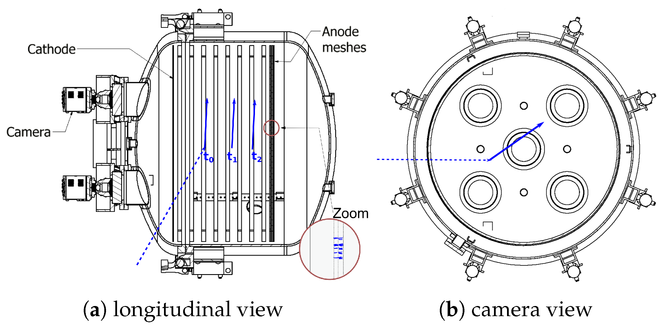
Figure 1.
Cross-sectional view of the HPTPC through (a) the plane parallel to the drift field E and (b) the plane perpendicular to E. A particle (dotted line) scatters on an atom or molecule in the gas at the time , ejects a charged particle from the nucleus, which, in turn, ionizes gas atoms along its trajectory (arrow, Figure (a)). These ionization electrons are moved by E towards the anode meshes and they are eventually amplified. The positions of these ionization electrons as they drift are labelled and . Photons that are produced during the amplification are then imaged by cameras and provide the 2D projection of the interaction (Figure (b)), the zoomed inlet in (a) illustrates where avalanches form and the photons are emitted.
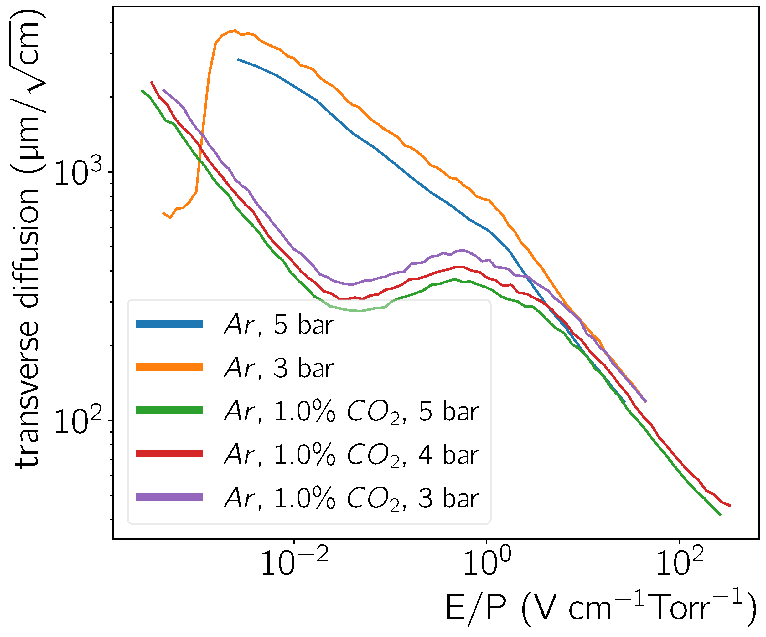
Figure 2.
Transverse diffusion for pure argon and different
mixtures that were simulated using
Magboltz [
23].
Figure 2.
Transverse diffusion for pure argon and different
mixtures that were simulated using
Magboltz [
23].
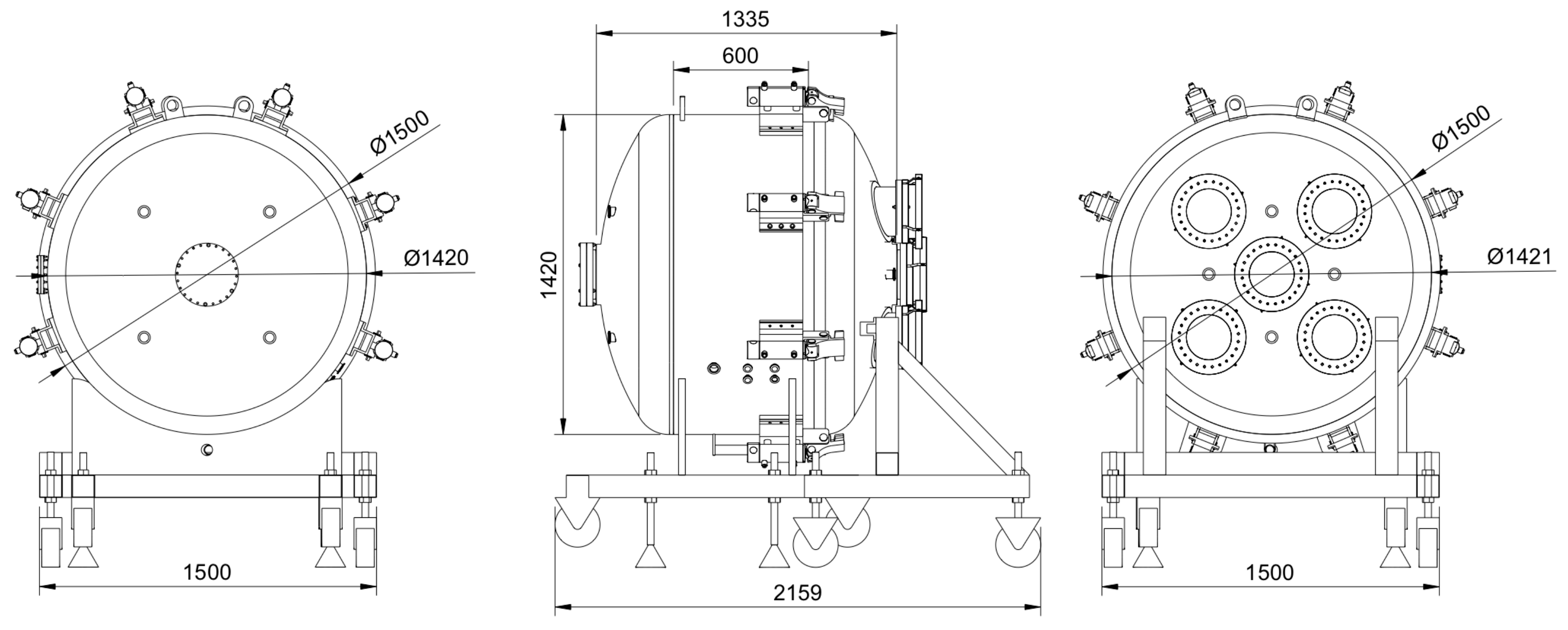
Figure 3.
Schematic drawings of the pressure vessel: end view of the back side (left), side view with the vessel door to the right (middle), and end view of the door side (right).
Figure 3.
Schematic drawings of the pressure vessel: end view of the back side (left), side view with the vessel door to the right (middle), and end view of the door side (right).
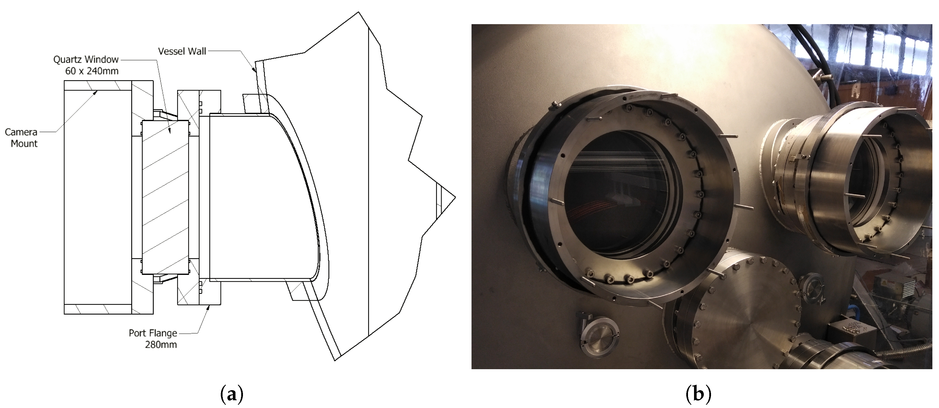
Figure 4.
(a) Drawing of the optical flange with the camera mount. The thick quartz is necessary for ensuring that the assembly can withstand the pressure difference between the vessel pressure and ambient pressure. (b) A photograph of the assembly with the camera removed.
Figure 4.
(a) Drawing of the optical flange with the camera mount. The thick quartz is necessary for ensuring that the assembly can withstand the pressure difference between the vessel pressure and ambient pressure. (b) A photograph of the assembly with the camera removed.
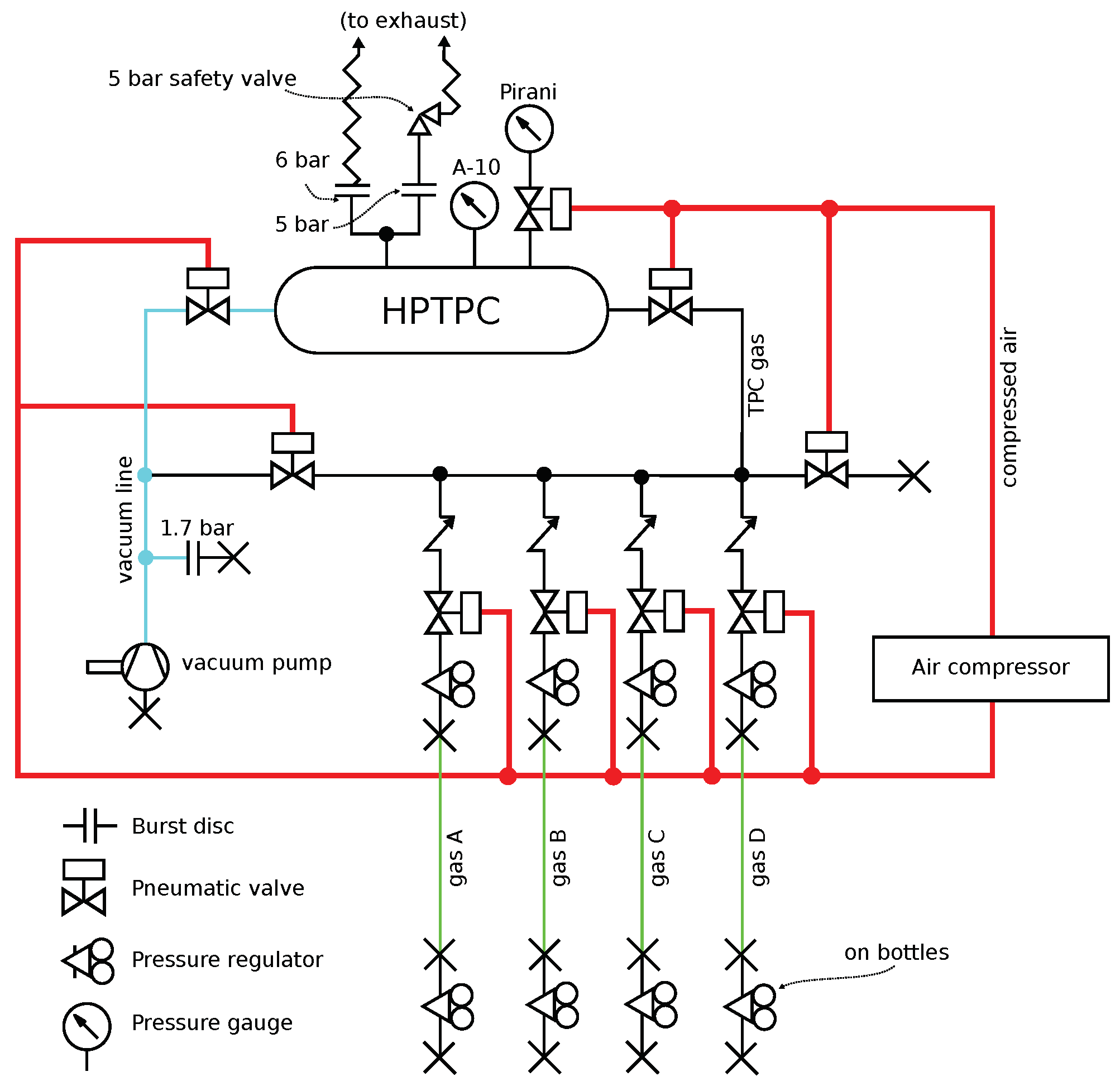
Figure 5.
Diagram of the gas fill and evacuation system for the HPTPC vessel.
Figure 5.
Diagram of the gas fill and evacuation system for the HPTPC vessel.
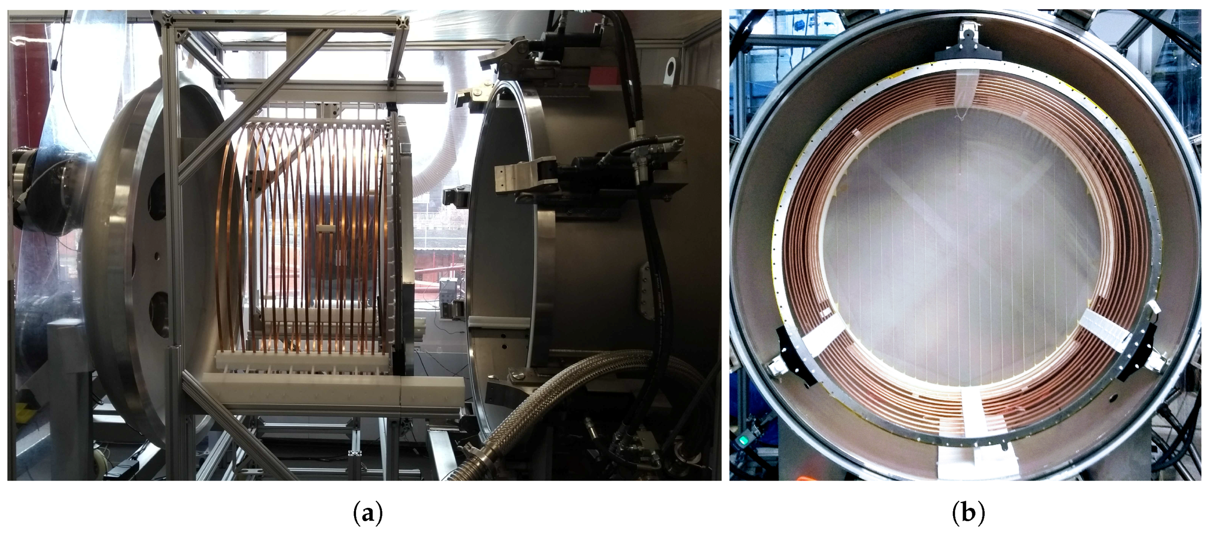
Figure 6.
(a) The field cage before insertion into the pressure vessel and (b) after insertion. The latter picture is photographed through the high-transparency cathode towards the amplification region and shows the full TPC.
Figure 6.
(a) The field cage before insertion into the pressure vessel and (b) after insertion. The latter picture is photographed through the high-transparency cathode towards the amplification region and shows the full TPC.
Figure 7.
Schematic of the circuit to bring high voltage (, ) to the anode meshes and decouple the signal from the high voltage lines. The signals are decoupled in bias boxes via a decoupling capacitor () and are then fed to the signal line (). These bias boxes also feature a protection and filtering circuit consisting of a bias resistor (), filter capacitor (), and input resistor at the detector input ( = 10 ).
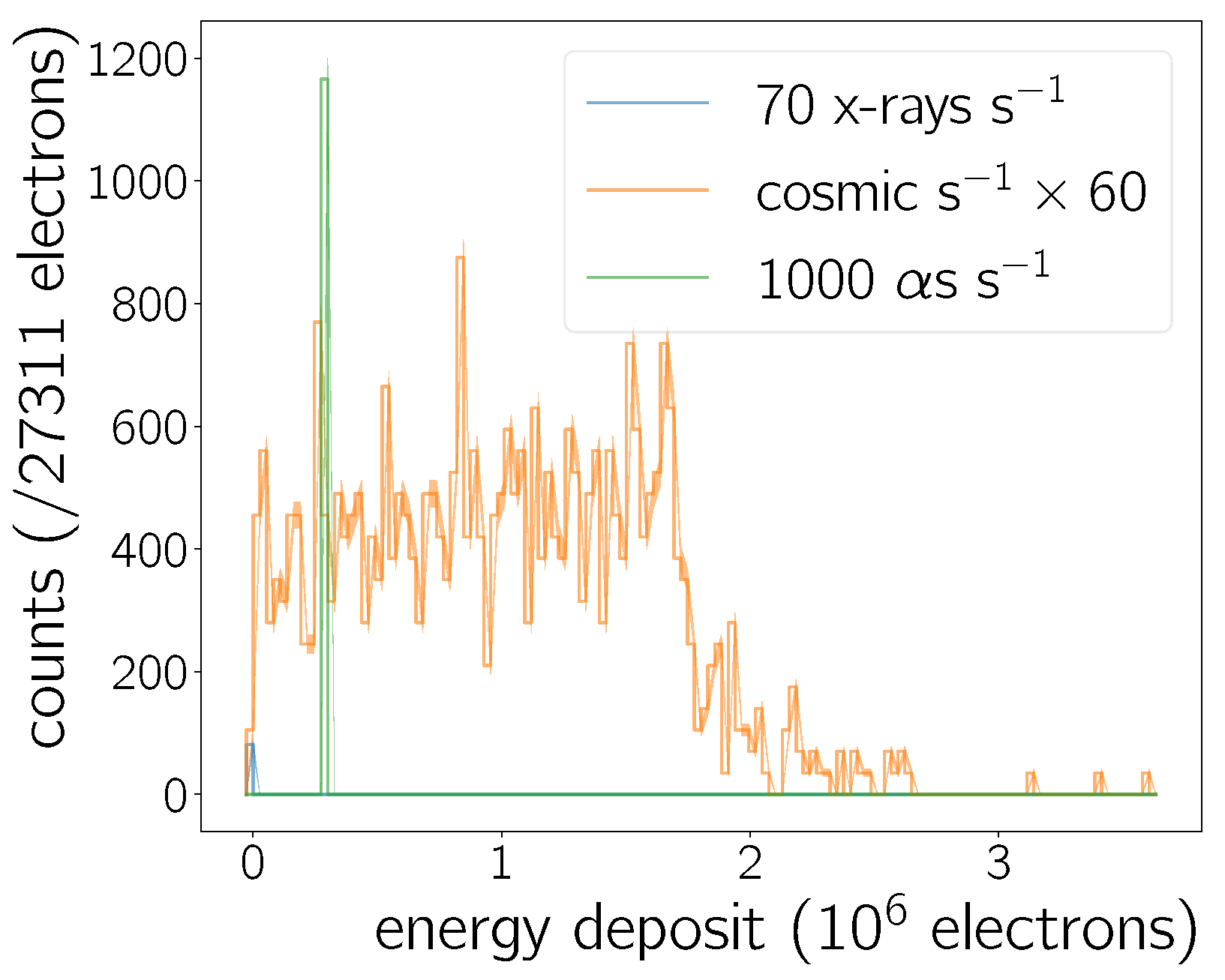
Figure 8.
The simulated energy deposits of
decay radiation and cosmic muons inside a gas volume filled with
(90/10). Energy deposits are measured in the number of liberated electrons during the energy deposit. This is the result of a
heed [
27] and
Garfield++ [
28] study taking the approximate layout of the HPTPC and the information in [
25,
26] into account.
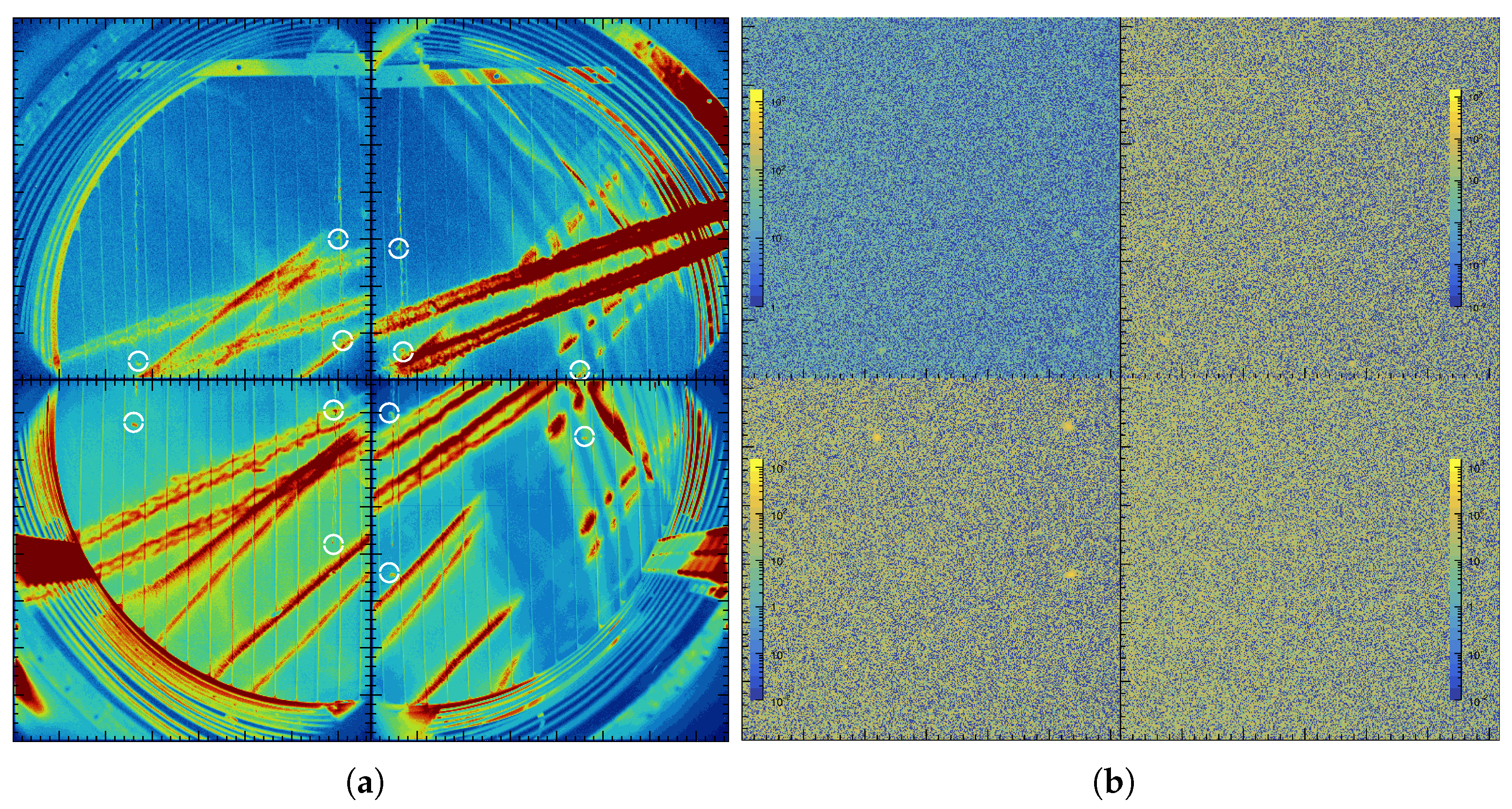
Figure 9.
CCD images showing the readout plane of the HPTPC; the vertical (horizontal) image axis points along the
y (
x) direction. The color encodes the light intensity in arbitrary units. (
a) Simultaneously recorded frames during a spark event. The locations of the
sources (marked by circles) inside the TPC are visible during the spark event as well as the field cage rings and the anode support,
cf. Figure 6b. (
b) The light yield from the calibration sources for 200
exposure time in pure Argon at 3 bar absolute pressure. The intensity of the image in the top left frame differs from the other three frames, because the corresponding camera has a different conversion gain.
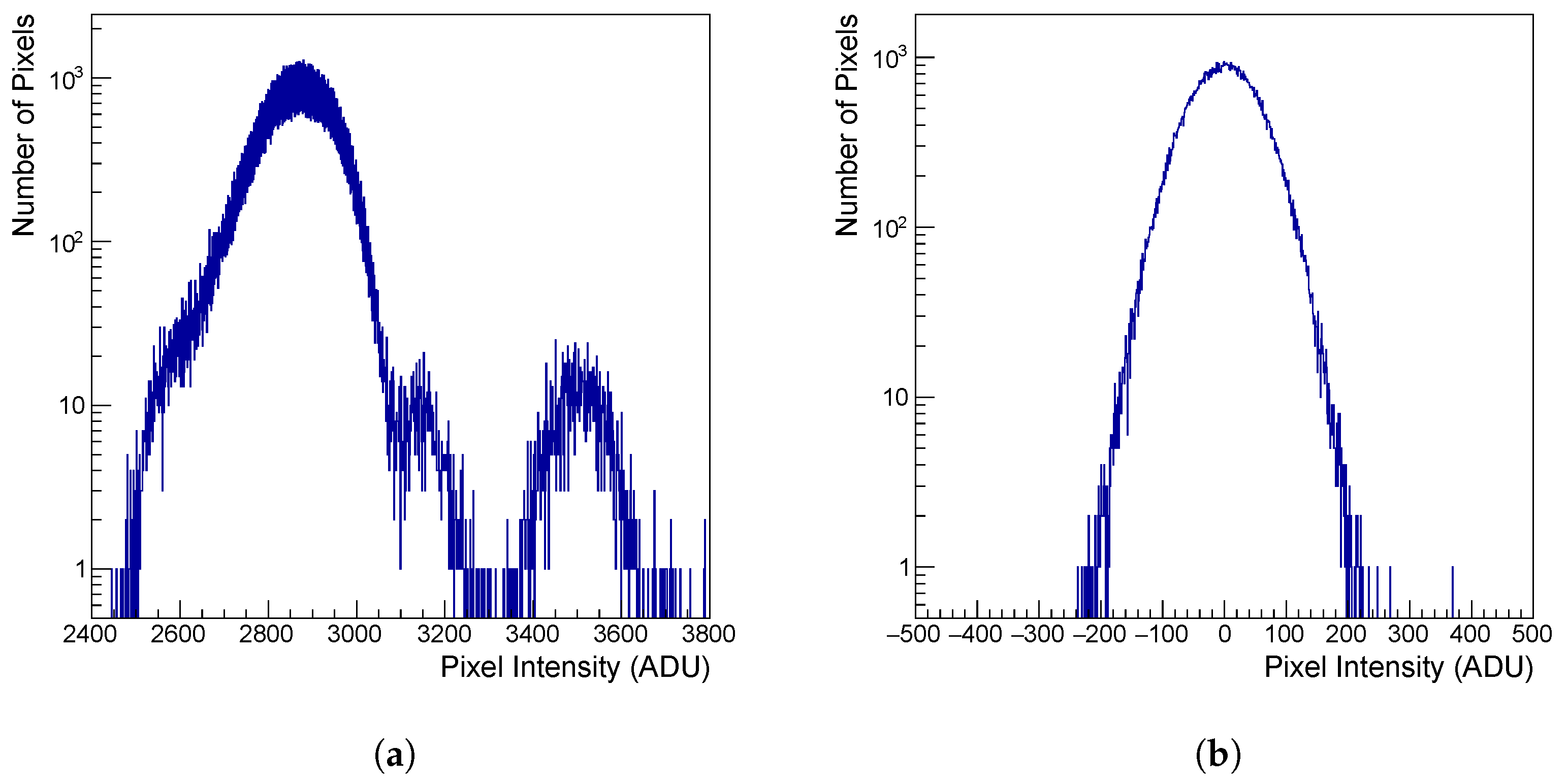
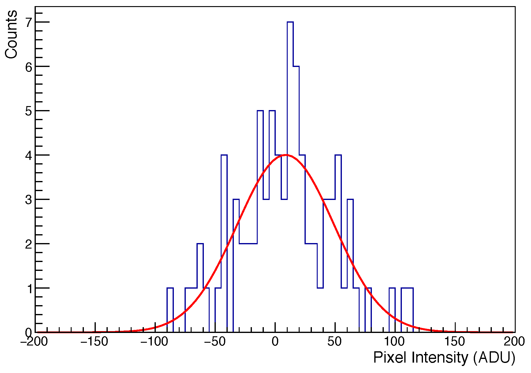
Figure 10.
Analogue-to-Digital Unit (ADU) distribution of all pixels of an exposure frame before (a) and after (b) bias subtraction.
Figure 10.
Analogue-to-Digital Unit (ADU) distribution of all pixels of an exposure frame before (a) and after (b) bias subtraction.
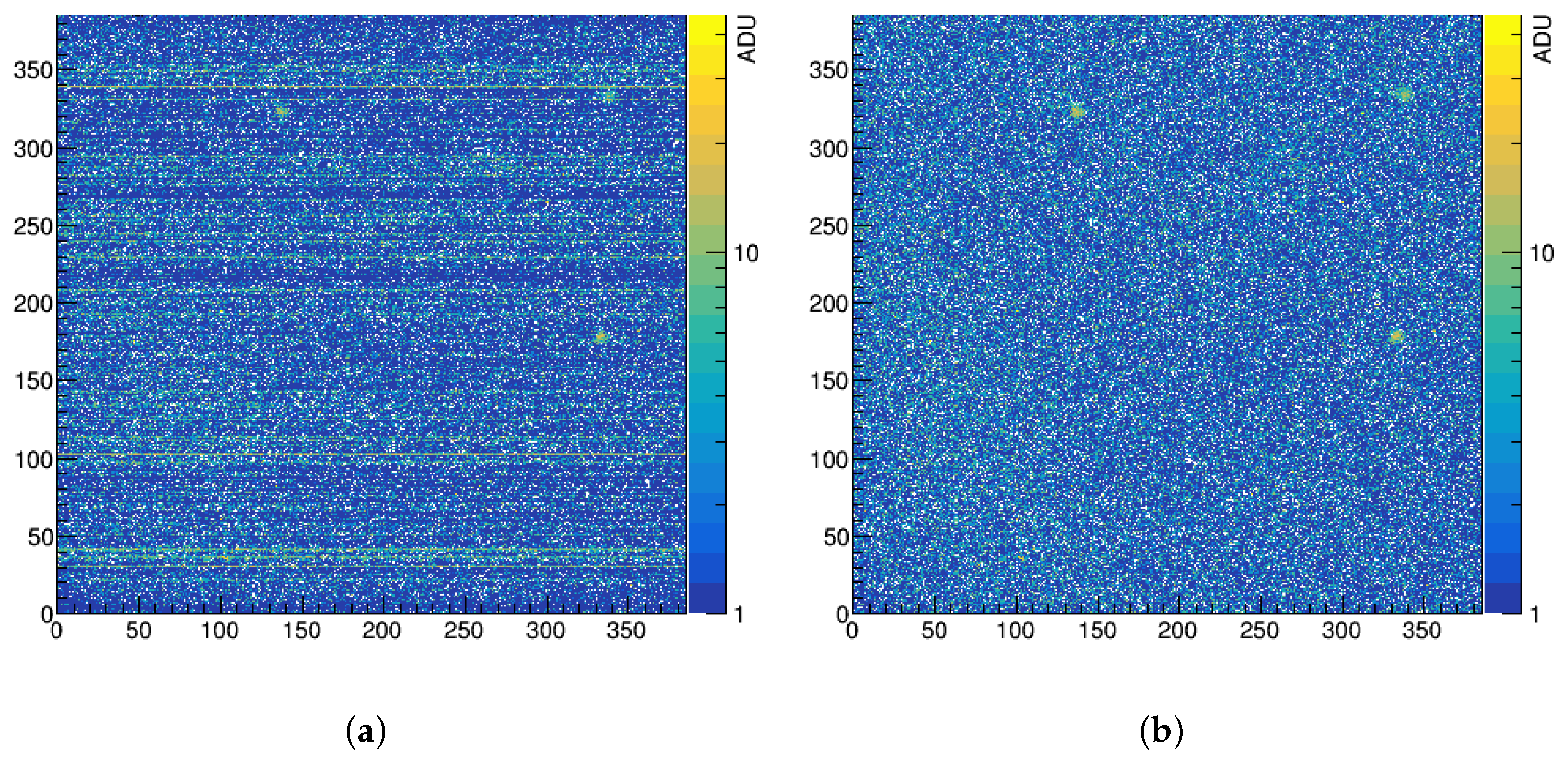
Figure 11.
Example of the average of 100 bias subtracted events with event and bias frame taken days apart (a) before row correction (demonstrating row CCD artefacts) (b) after row correction (demonstration correction of row CCD artefacts). The colour in both plots encodes the value at the position of a pixel, while the horizontal and vertical axis shows the y and x coordinate, respectively.
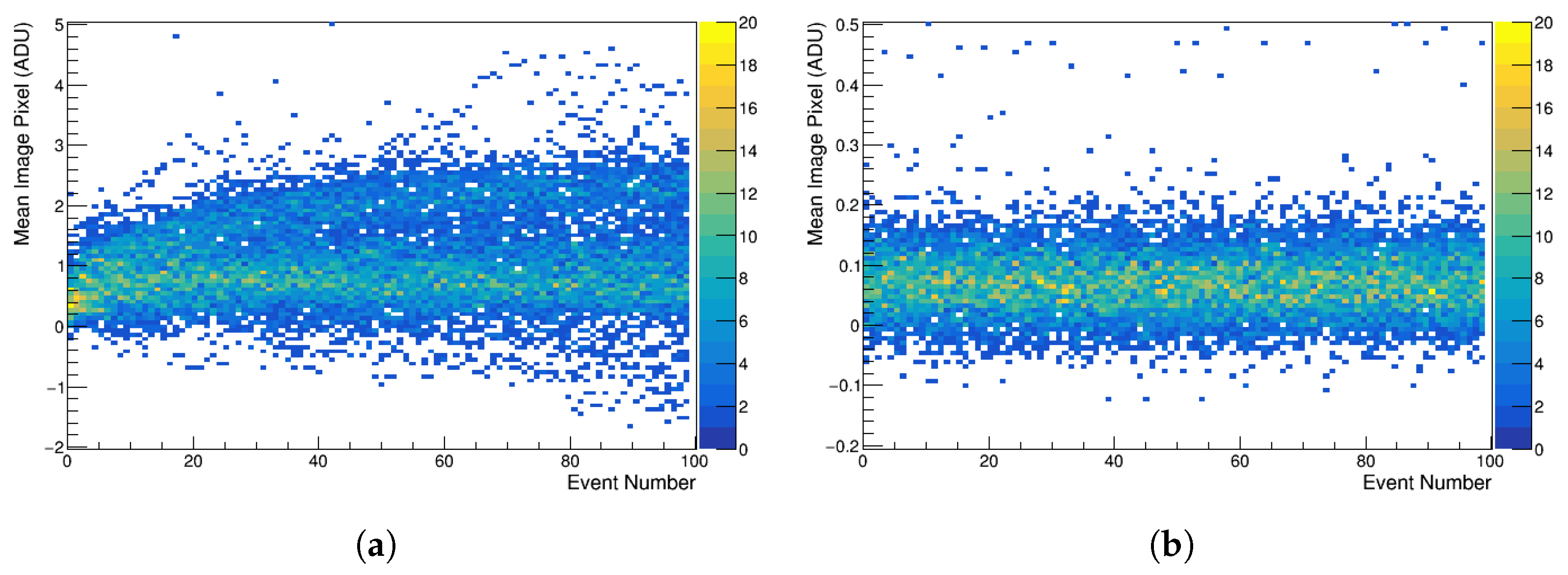
Figure 12.
Mean value of exposure frames versus event number for 150 runs (of 100 events, i.e., frames) taken over a number of days (a) before row correction (demonstrating pixel pedestal drift) (b) after row correction. The latter demonstrates the correction of the pedestal drift by the row correction procedure.
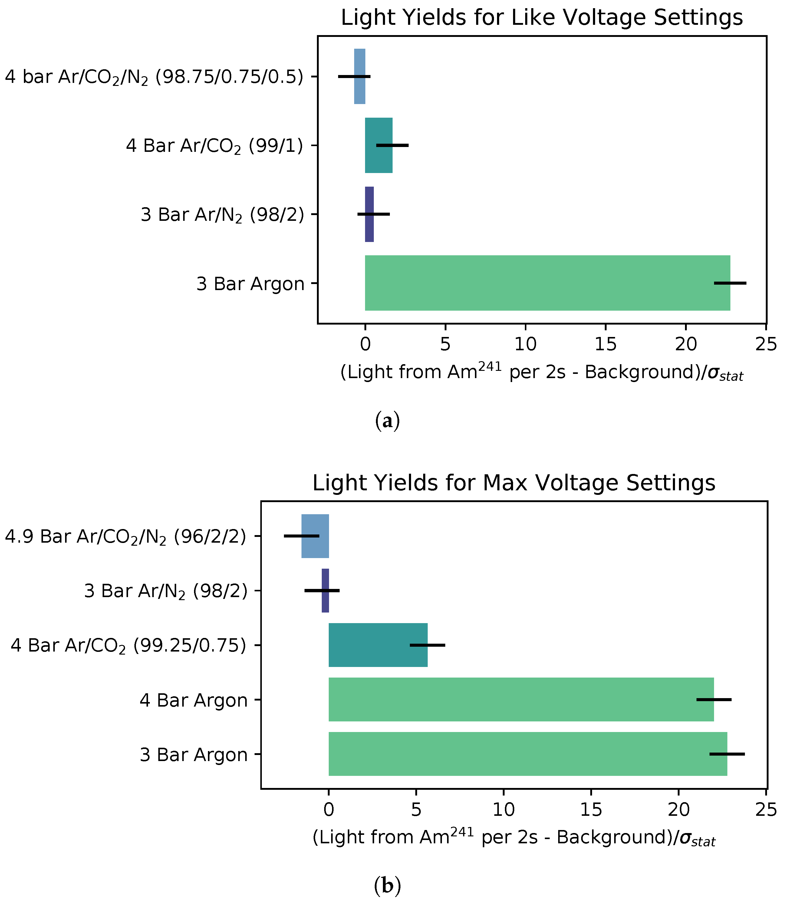
Figure 13.
Light yield measured for an
Am source with different gas mixtures (
a) at near constant anode and cathode voltages and (
b) the maximal light yield achieved.
Table 1 lists the voltages used during these measurements.
Figure 13.
Light yield measured for an
Am source with different gas mixtures (
a) at near constant anode and cathode voltages and (
b) the maximal light yield achieved.
Table 1 lists the voltages used during these measurements.
Figure 14.
The intensity distribution of pixels within the source box for a single event.
Figure 14.
The intensity distribution of pixels within the source box for a single event.
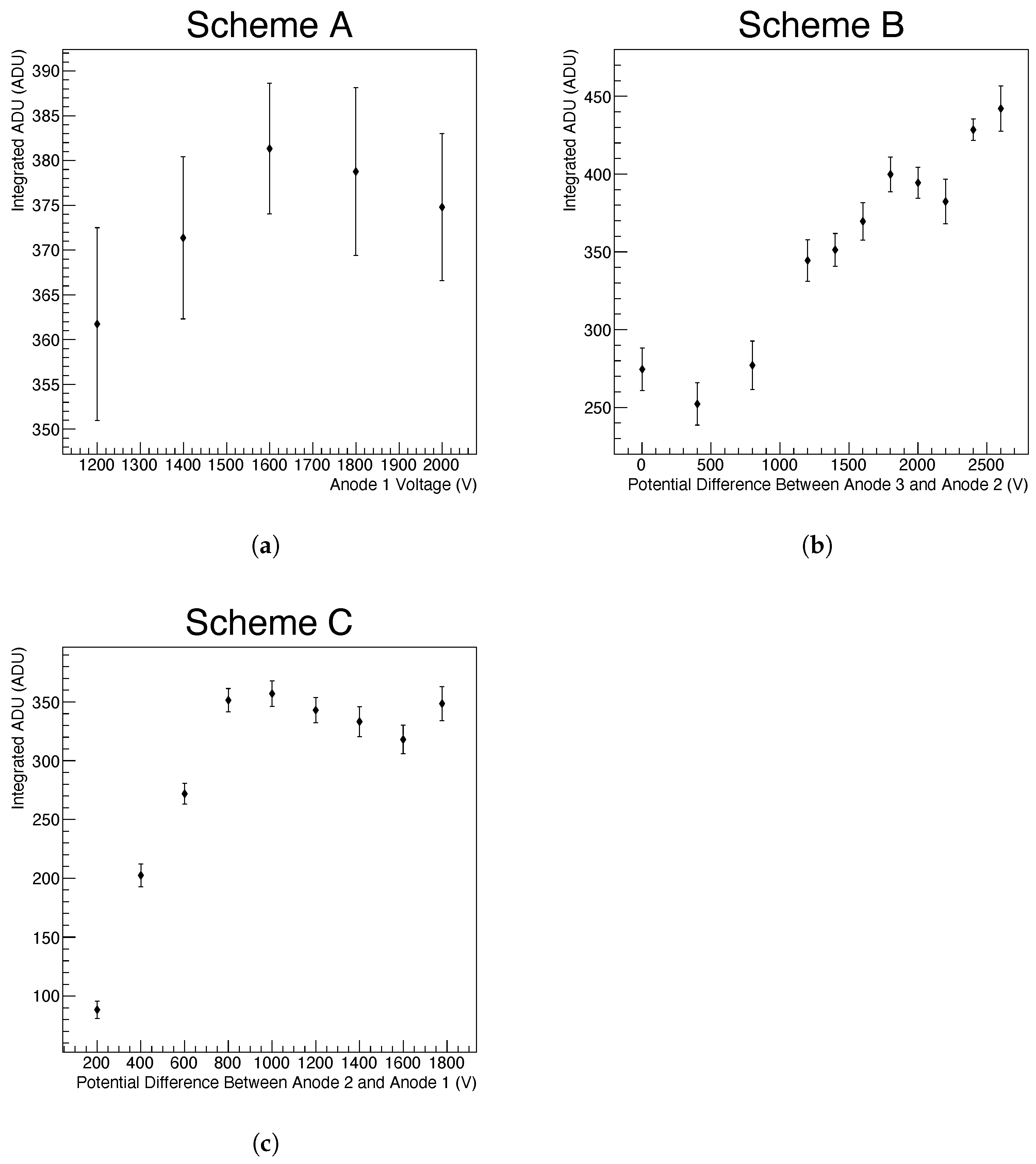
Figure 15.
Light gain measurements of integrated ADU from source (a) vs. anode 1 voltage where the voltage difference between anode 1 and 2 (anode 2 and 3) is kept constant at , (b) vs. voltage potential difference between anode 2 and anode 3 whilst the voltage difference between anodes 1 and 2 is maintained at 1200 , and (c) vs. potential difference between anodes 1 and 2 whilst the potential difference between anode 2 and 3 is maintained at 1200 . All of the measurements have been performed in the same fill of pure argon at 3 bar absolute pressure.
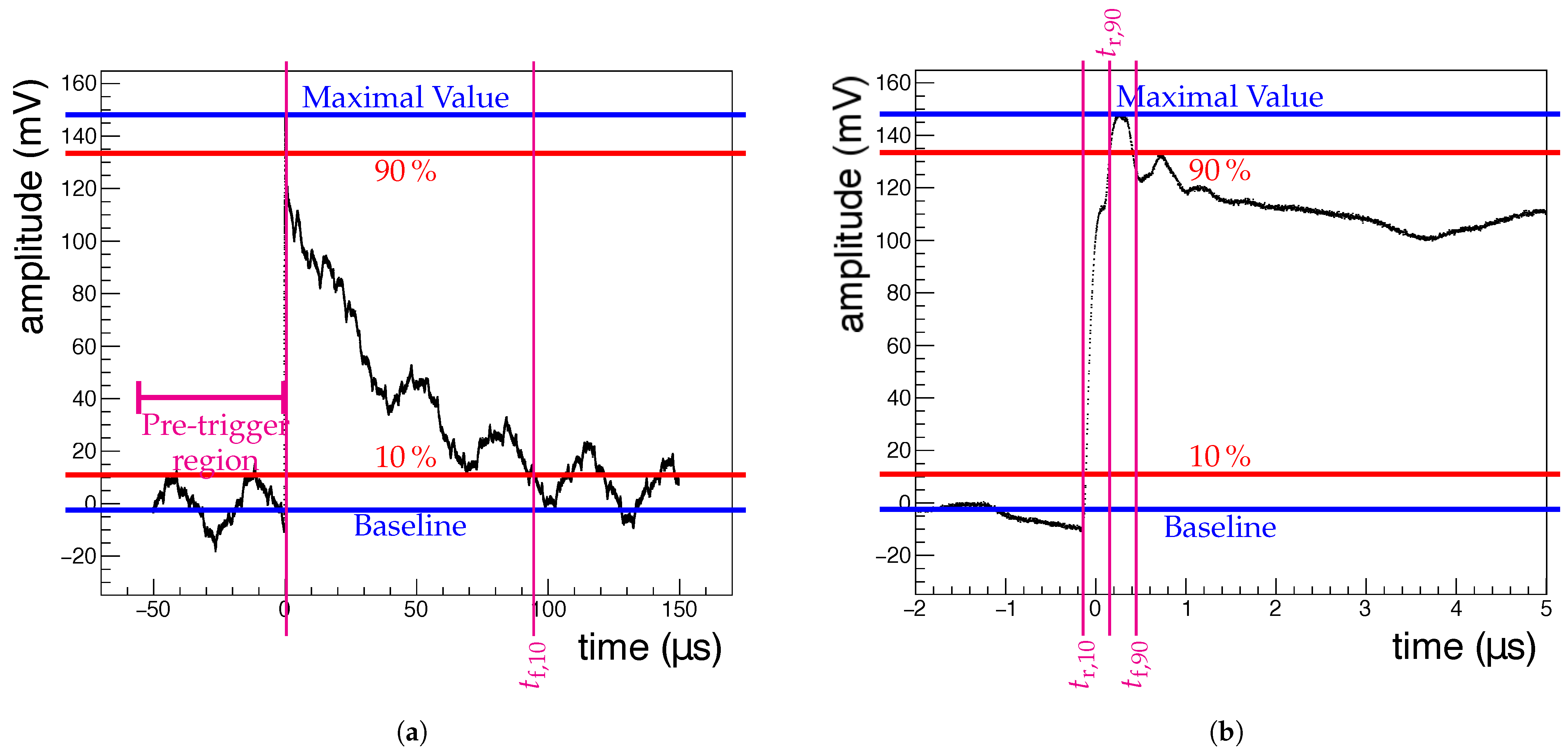
Figure 16.
Example for a charge signal, a waveform—(a) and (b) zoom—with some of its defining features indicated. See the text for more explanations. The first vertical line in (a) shows the approximate position of all the vertical lines in the zoomed plot in (b).
Figure 16.
Example for a charge signal, a waveform—(a) and (b) zoom—with some of its defining features indicated. See the text for more explanations. The first vertical line in (a) shows the approximate position of all the vertical lines in the zoomed plot in (b).
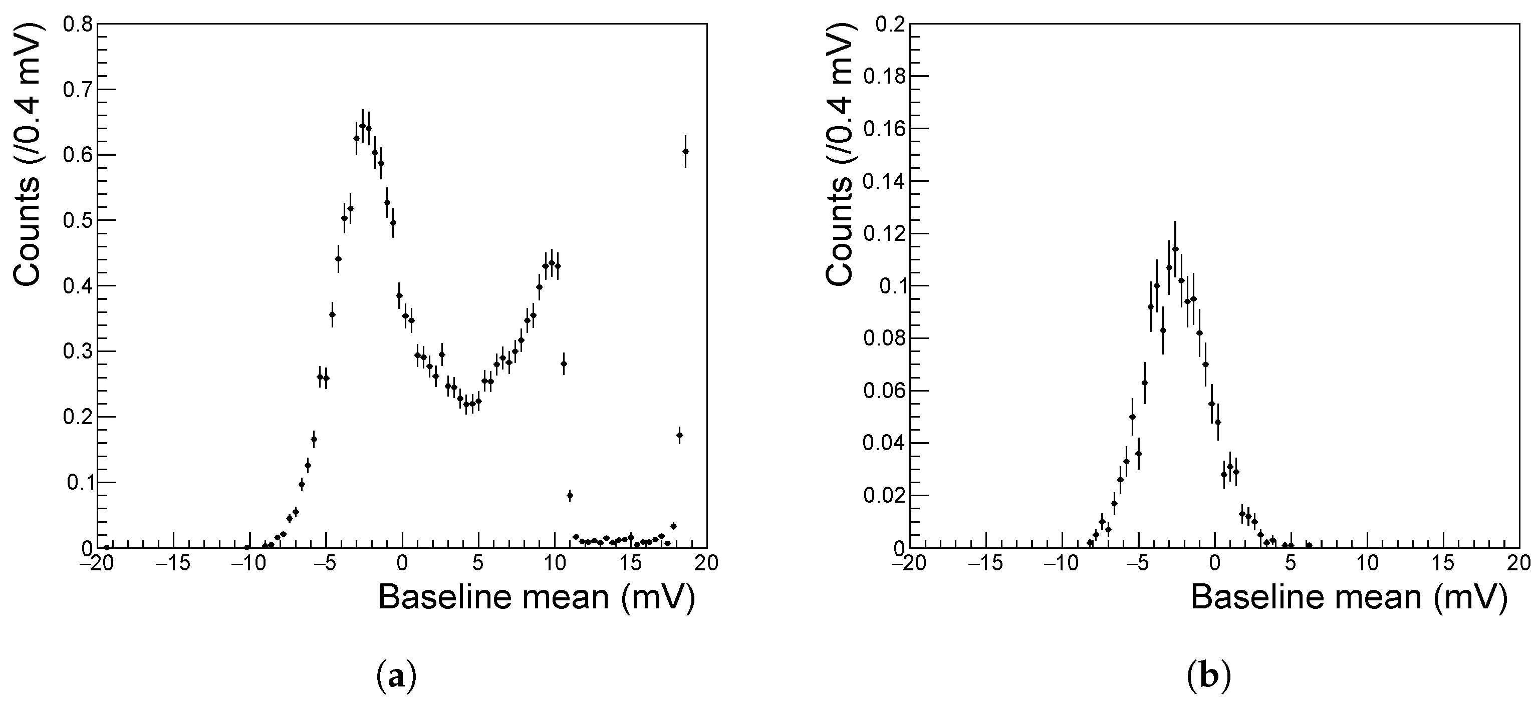
Figure 17.
Anode 1 Baseline spectrum (a) before cleaning, and (b) after cleaning. Waveforms with large Baseline values are cut, which removes spark events.
Figure 17.
Anode 1 Baseline spectrum (a) before cleaning, and (b) after cleaning. Waveforms with large Baseline values are cut, which removes spark events.
Figure 18.
Waveform of a test pulse, coupled into the anode 1 mesh and the resulting amplified pulses (CR-112), as digitized by the HPTPC’s data acquisition system.
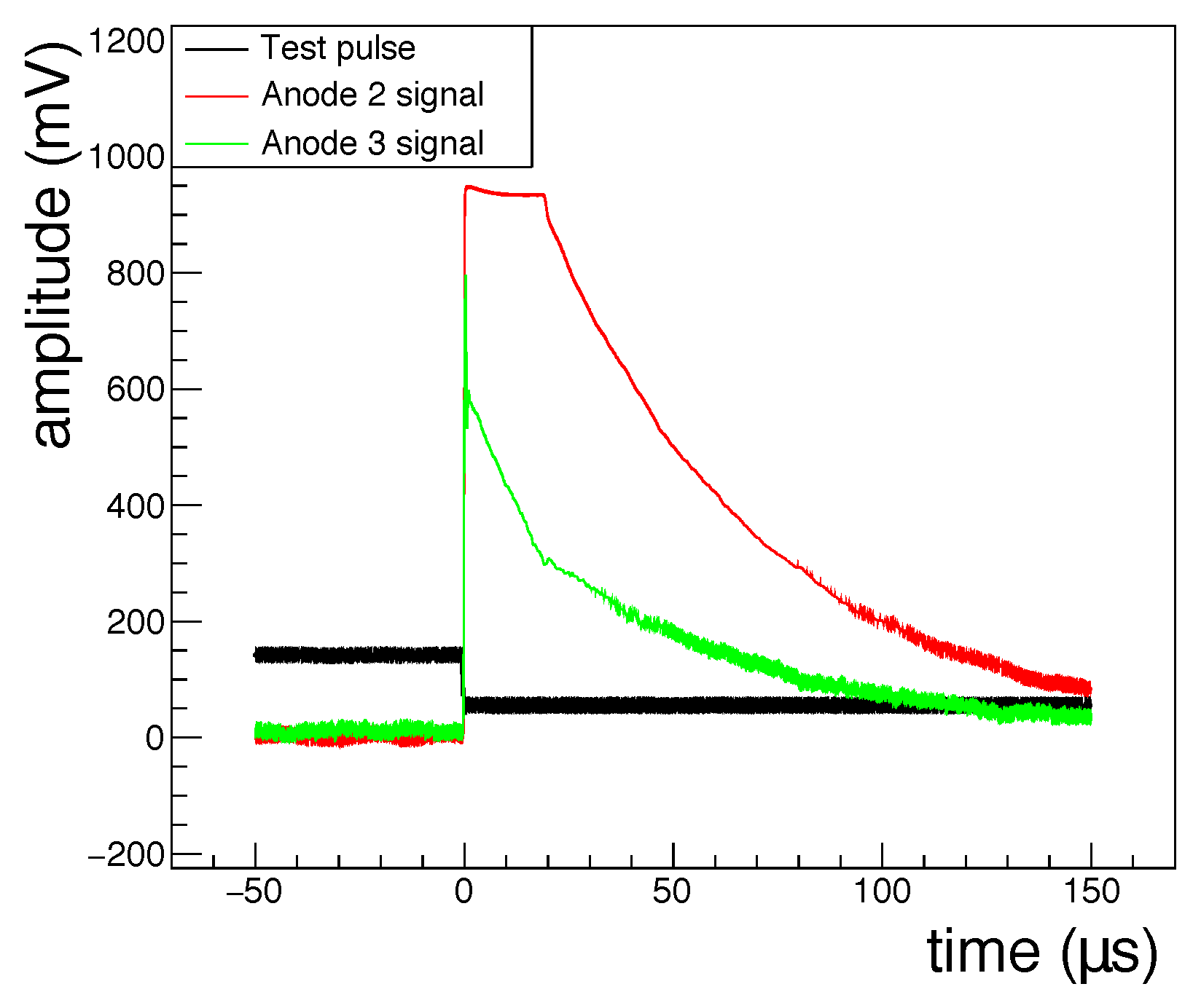
Figure 18.
Waveform of a test pulse, coupled into the anode 1 mesh and the resulting amplified pulses (CR-112), as digitized by the HPTPC’s data acquisition system.
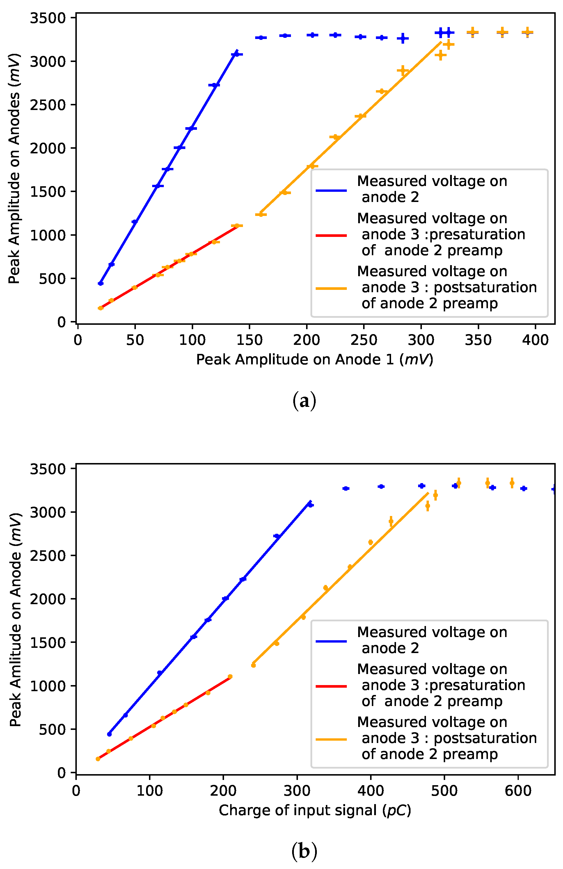
Figure 19.
Peak height () measured by the anode 2 and anode 3 readout channel (with pre-amplifier) for test pulses injected into the amplification region via the anode 1 mesh. Both plots show the same data with different units on the horizontal axis: (a) as function of input test pules signal height () and (b) as a function of the charge seen at the pre-amplifier input. One polynomial of order () one is fitted to the anode 2 (blue) measurement and two separate s are fitted to the different regions on anode 3. One in the pre-saturation region of the anode 2 pre-amplifier (red) and one in the post-saturation region of anode 2 pre-amplifier (orange).
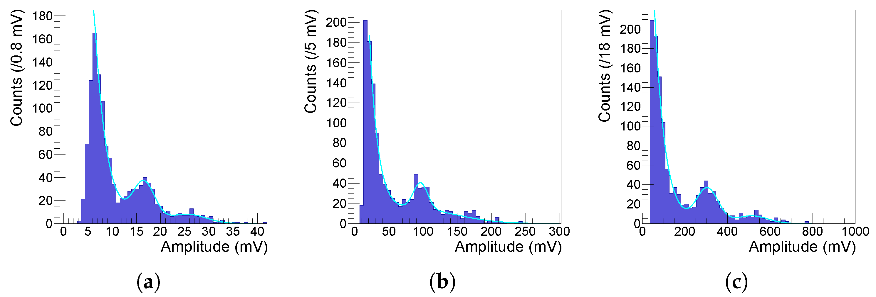
Figure 20.
The waveform amplitude spectra for anodes (a) 1, (b) 2, and (c) 3. The counts shown on the vertical axis are normalized to the time of one CCD exposure, i.e., 2 . The spectra are fitted with an exponential plus two Gaussian functions. The amplitude spectra shown are summed data over 15 consecutive runs taken at the same voltage settings, , , , and .
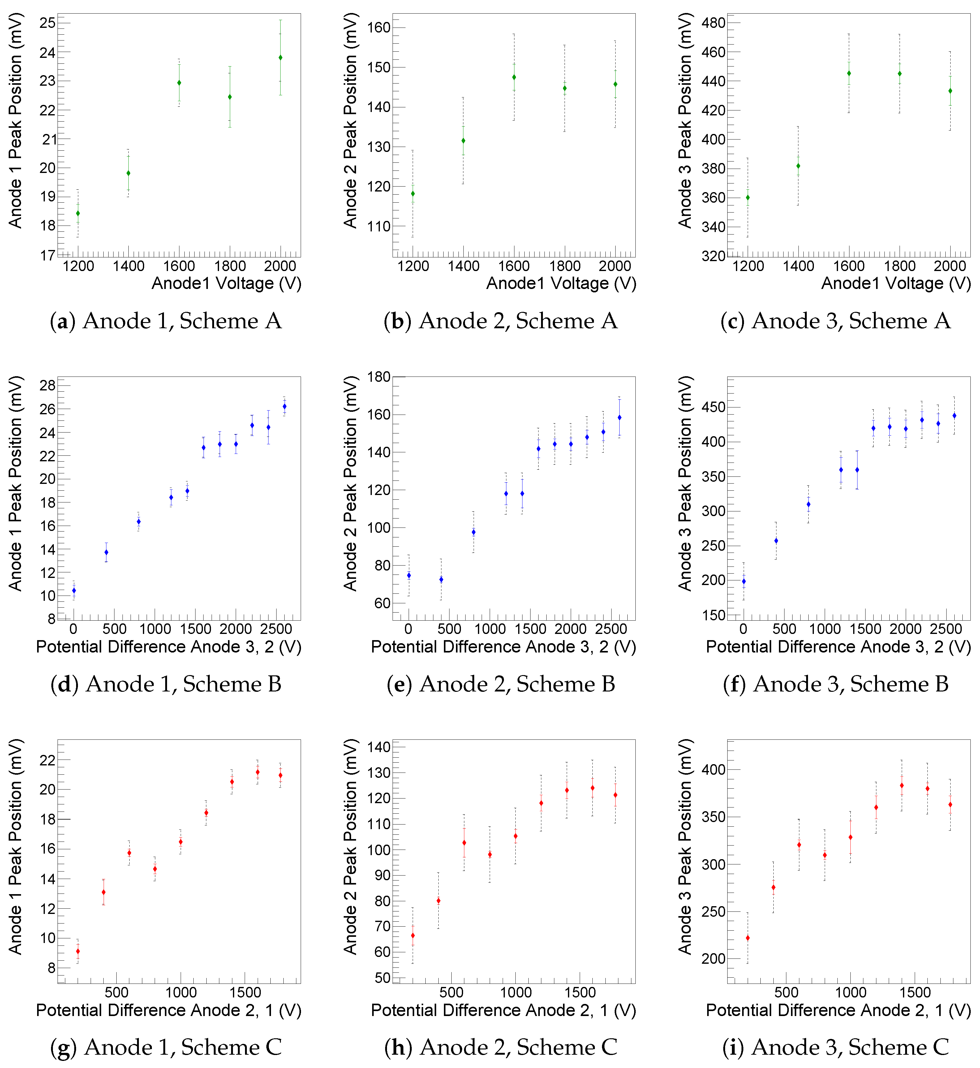
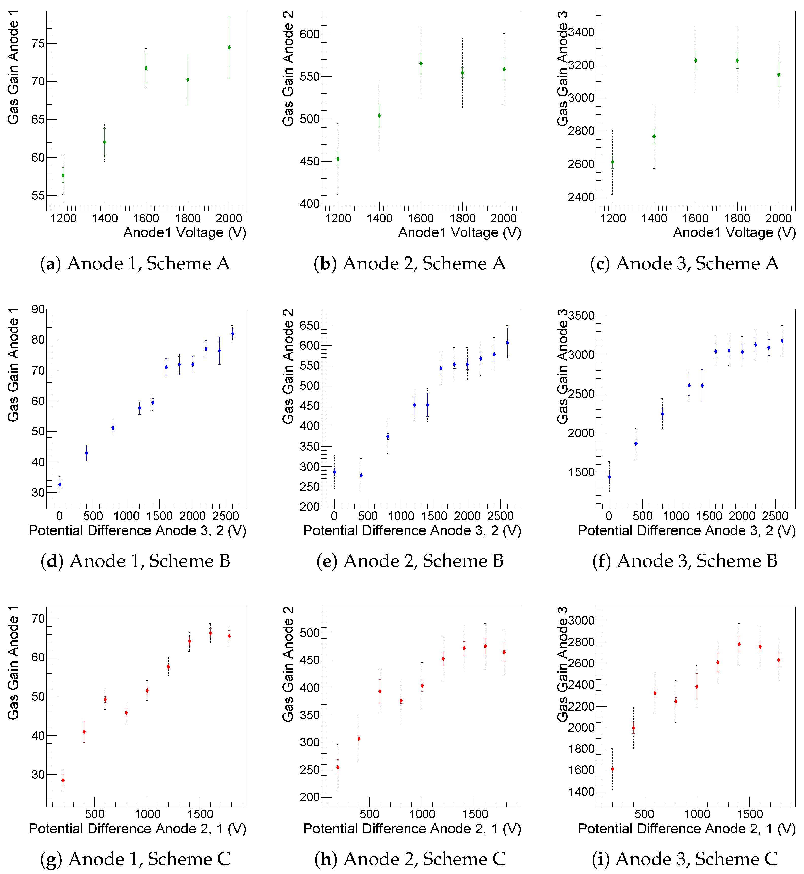
Figure 21.
Plots of the position of the -peak in the respective amplitude spectra. In the first row (a–c) the peak position is plotted vs. anode 1 voltage (Scheme A). During Scheme A, the voltages of all three anodes are increased in steps of 200 , while the potential difference between anodes is kept constant. In the second row (Scheme B: d–f) the peak position is plotted vs. the potential difference between anodes 2 and 3 (). During the measurement , and are kept constant. Third row (Scheme C: g–i): Peak position vs. the potential difference between anodes 1 and 2 (), while and are kept constant. All of the measurements have been made in the same gas fill of 3 bar absolute of pure argon.
Figure 22.
Plots of the calculated gas gain vs. either anode voltage or inter-anode voltage difference. The gain is calculated from the data shown in the respective plot in
Figure 21. First row (
a–
c): Scheme A, gain vs. anode 1 voltage (
),
,
, and
are increased by the same amount, whilst
. Second row (
d–
f): Scheme B, gain vs. the voltage difference between anode 2 and 3 (
),
, and
are increased, whilst
and
. Third row (
g–
i): Scheme C, gain vs. the anode 1 to anode 2 voltage differences (
),
,
, and
are increased whilst keeping
and
constant. All of the data have been taken in the same gas fill of 3 bar absolute of pure argon.
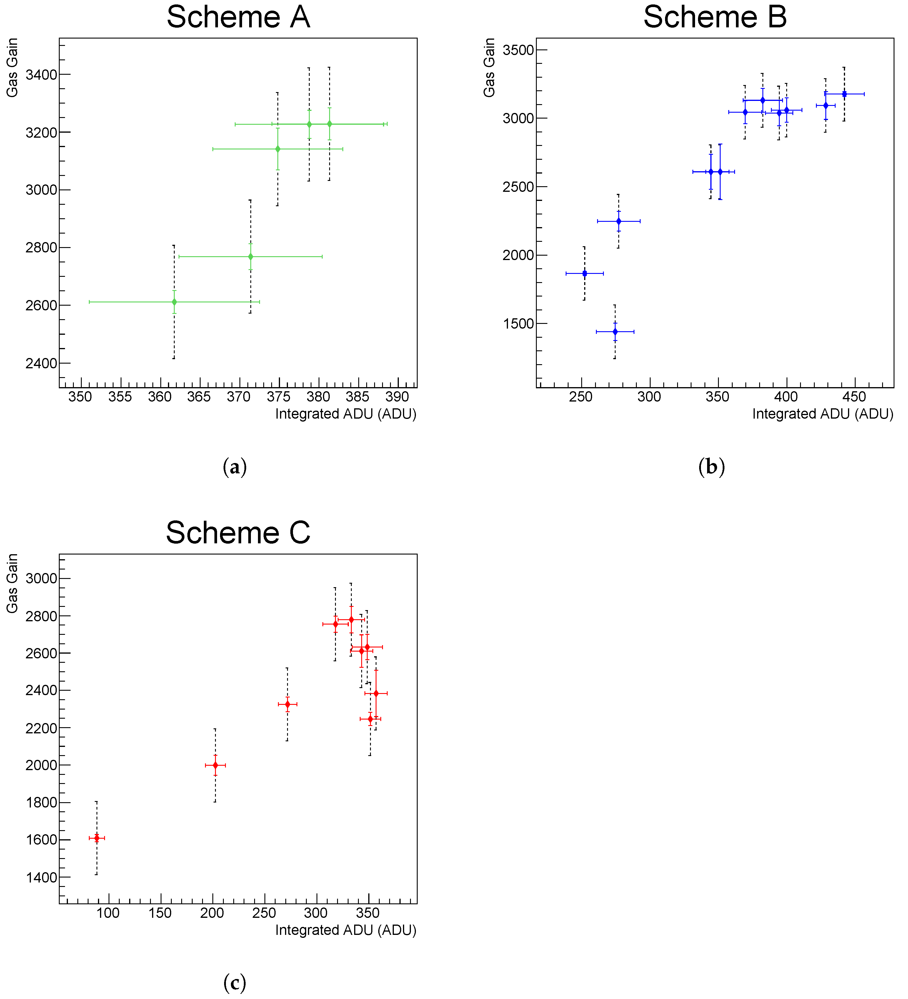
Figure 23.
Measured light intensity (Integrated
) (
Figure 15) plotted against the gas gain measured in the charge readout on anode 3 (
Figure 22, right column) for Scheme A (
a), Scheme B (
b), and Scheme C (
c).
Figure 23.
Measured light intensity (Integrated
) (
Figure 15) plotted against the gas gain measured in the charge readout on anode 3 (
Figure 22, right column) for Scheme A (
a), Scheme B (
b), and Scheme C (
c).
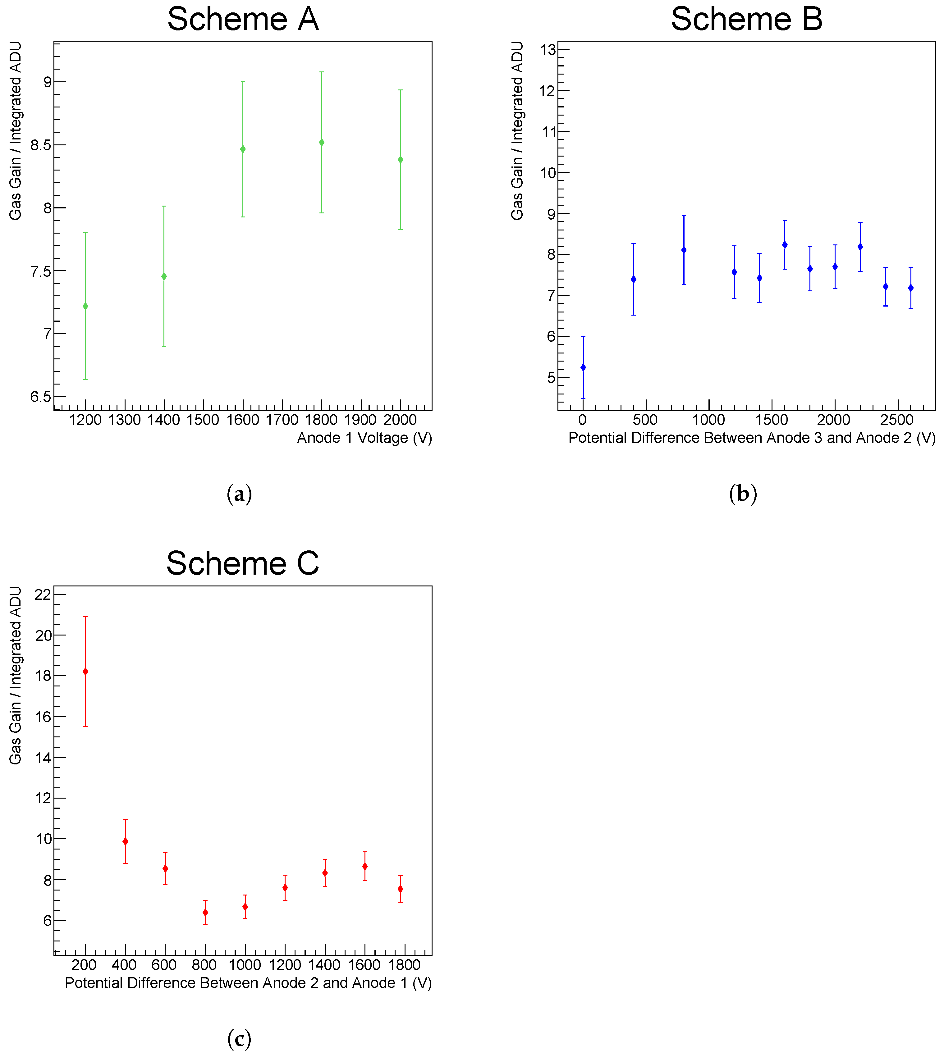
Figure 24.
Ratio of gas gain measured in the amplification region at anode 3 (
Figure 22, right column) to the measured intensity (integrated
) (
Figure 15) vs. (
a) anode 1 voltage (
), where the voltage differences between the meshes is always
(
b) potential difference between anode 2 and anode 3 (
), while the anode 1 and 2 voltages are kept constant (
c) potential difference between anodes 1 and 2 (
), while
is kept constant and
is maintained at 1200
.
Table 1.
Voltage settings for the result plot shown in
Figure 13: the
top table shows the voltages used for the settings that are shown in
Figure 13a, while the
bottom table shows the settings used for the data shown in
Figure 13b. The absolute pressure is quoted.
Table 1.
Voltage settings for the result plot shown in
Figure 13: the
top table shows the voltages used for the settings that are shown in
Figure 13a, while the
bottom table shows the settings used for the data shown in
Figure 13b. The absolute pressure is quoted.
| mixture or gas | P | | | | |
| (98.75/0.75/0.5) | 4 bar | 1000 | 2000 | 4000 | −7000 |
| (99/1) | 4 bar | 1200 | 2400 | 4000 | −7000 |
| (98/2) | 3 bar | 1200 | 2800 | 4000 | −7000 |
| 3 bar | 1500 | 2100 | 4500 | −5250 |
| mixture or gas | P | | | | |
| (96/2/2) | bar | 3000 | 5900 | 7600 | −8500 |
| (98/2) | 3 bar | 1550 | 3300 | 5000 | −5000 |
| (99.25/0.75) | 4 bar | 1200 | 2500 | 4800 | −7000 |
| 4 bar | 1000 | 1750 | 2800 | −5700 |
| 3 bar | 1500 | 2100 | 4500 | −5250 |
Table 2.
The fraction of analyzed waveforms rejected for each data cleaning cut for a run where no sparking was observed.
Table 2.
The fraction of analyzed waveforms rejected for each data cleaning cut for a run where no sparking was observed.
| Cut | Surviving Signals |
|---|
| | Single Cut | Cuts Applied Subsequently |
|---|
| No Cuts | 100% | 100% |
| 99.97% | 99.97% |
| 99.97% | 99.97% |
| 99.99% | 99.97% |
| 11.25% | 11.23% |
| 61.23% | 9.59% |
| 20.56% | 9.59% |
Table 3.
Fraction of analyzed waveforms rejected for each data cleaning cut for a run containing spark events.
Table 3.
Fraction of analyzed waveforms rejected for each data cleaning cut for a run containing spark events.
| Cut | Surviving Signals |
|---|
| | Single Cut | Cuts Applied Subsequently |
|---|
| No Cuts | 100% | 100% |
| 53.26% | 53.26% |
| 26.85% | 26.85% |
| 68.29% | 26.85% |
| 5.64% | 5.22% |
| 51.53% | 4.35% |
| 14.92% | 4.25% |
Table 4.
Mesh capacitances determined by a fit [
29] and by a direct measurement with a multimeter.
Table 4.
Mesh capacitances determined by a fit [
29] and by a direct measurement with a multimeter.
| Measurement Taken | Capacitance’s between Anode 1/2 [] | of Anode 1/2 | Capacitances between Anode 2/3 [] | of Anode 2/3 | Capacitances between Anode 1/3 [] |
|---|
| fit | 7.3 ± 0.3 | 0.76 | 4.4 ± 0.4 | 0.35 | - |
| Multimeter reading | 6.06 ± 0.05 | - | 3.72 ± 0.05 | - | 2.16 ± 0.05 |
Table 5.
Using the measured pre-amplifier without the circuit response (
) and the measurements of the pre-amplifiers connected to the detector
, the circuit response modification-factor
f is determined [
29].
Table 5.
Using the measured pre-amplifier without the circuit response (
) and the measurements of the pre-amplifiers connected to the detector
, the circuit response modification-factor
f is determined [
29].
| Anode | | Modification Factor |
|---|
| [mv/pC] | |
|---|
| anode 2 | 9.8 ± 0.1 | 0.754 ± 0.007 |
| anode 3 Pre-saturation | 5.18 ± 0.07 | 0.398 ± 0.005 |
| anode 3 Post-saturation | 8.3 ± 0.4 | 0.64 ± 0.03 |
Table 6.
The charge gain measured at the highest at lowest voltage settings of each voltage scheme.
Table 6.
The charge gain measured at the highest at lowest voltage settings of each voltage scheme.
| Scheme | Voltage Setting (A1 / A2 / A3) [V] | Gas Gain at Anode 3 at Voltage Setting |
|---|
| Lowest | Highest | at Lowest Setting | at Highest Setting |
|---|
| A | 1200 / 2400 / 3600 | 2000 / 3200 / 4400 | (2.61 ± 0.20) × 103 | (3.14 ± 0.20) × 103 |
| B | 1200 / 2400 / 2400 | 1200 / 3400 / 5000 | (1.44 ± 0.20) × 103 | (3.18 ± 0.20) × 103 |
| C | 1200 / 1400 / 2600 | 1200 / 3000 / 4200 | (1.61 ± 0.20) × 103 | (2.63 ± 0.20) × 103 |


 ,
, 


