Evaluation of Microwave Characterization Methods for Additively Manufactured Materials

 , , , , ,
Abstract
:1. Introduction
2. Microwave Characterization Methods
2.1. Nonresonant Methods
2.1.1. Reflection Methods
2.1.2. Transmission/Reflection Methods
2.2. Resonant Methods
2.2.1. MUT as a Resonator Method
2.2.2. Resonant Perturbation Methods
3. Commercial Methods for Characterization
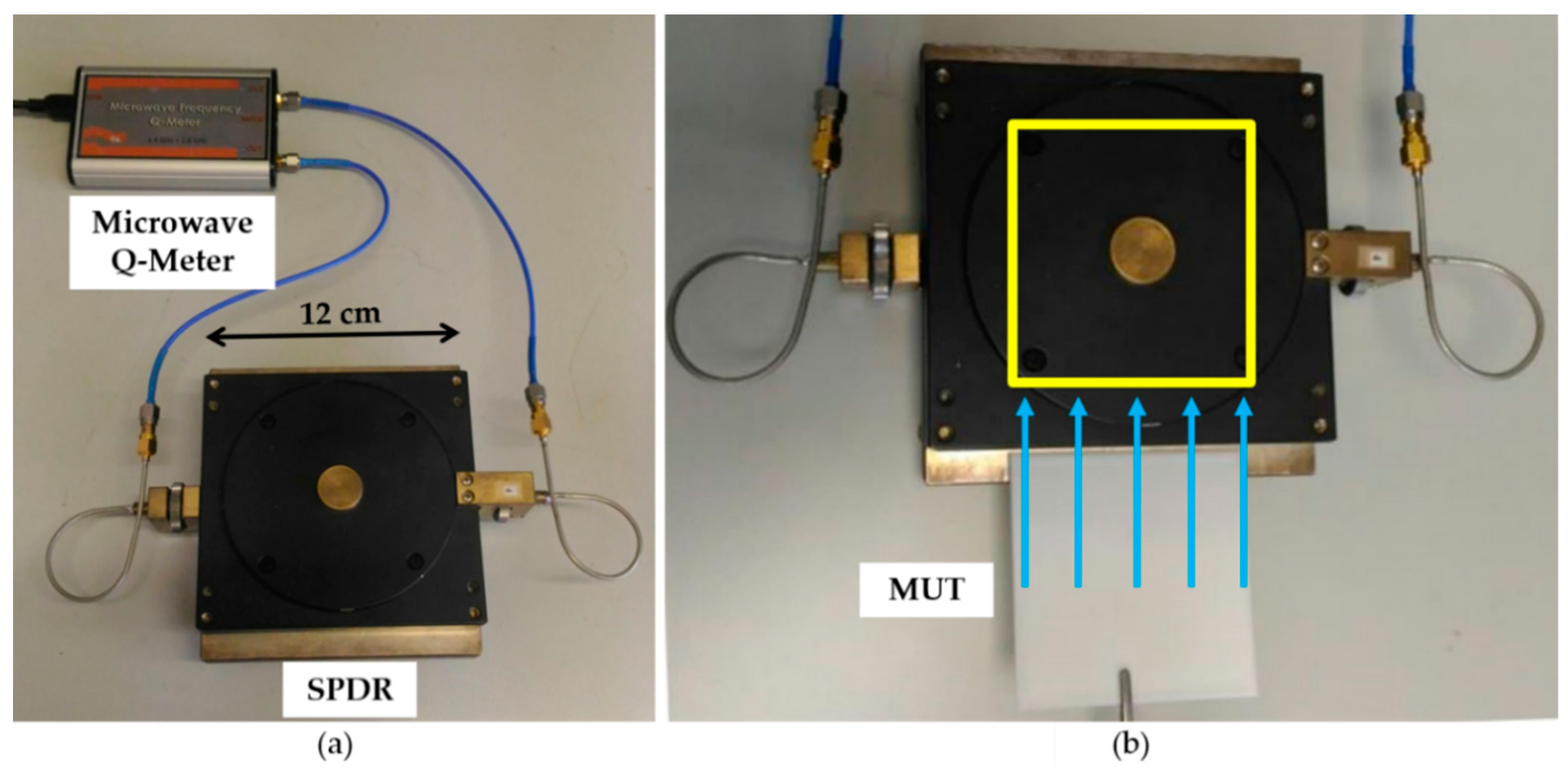
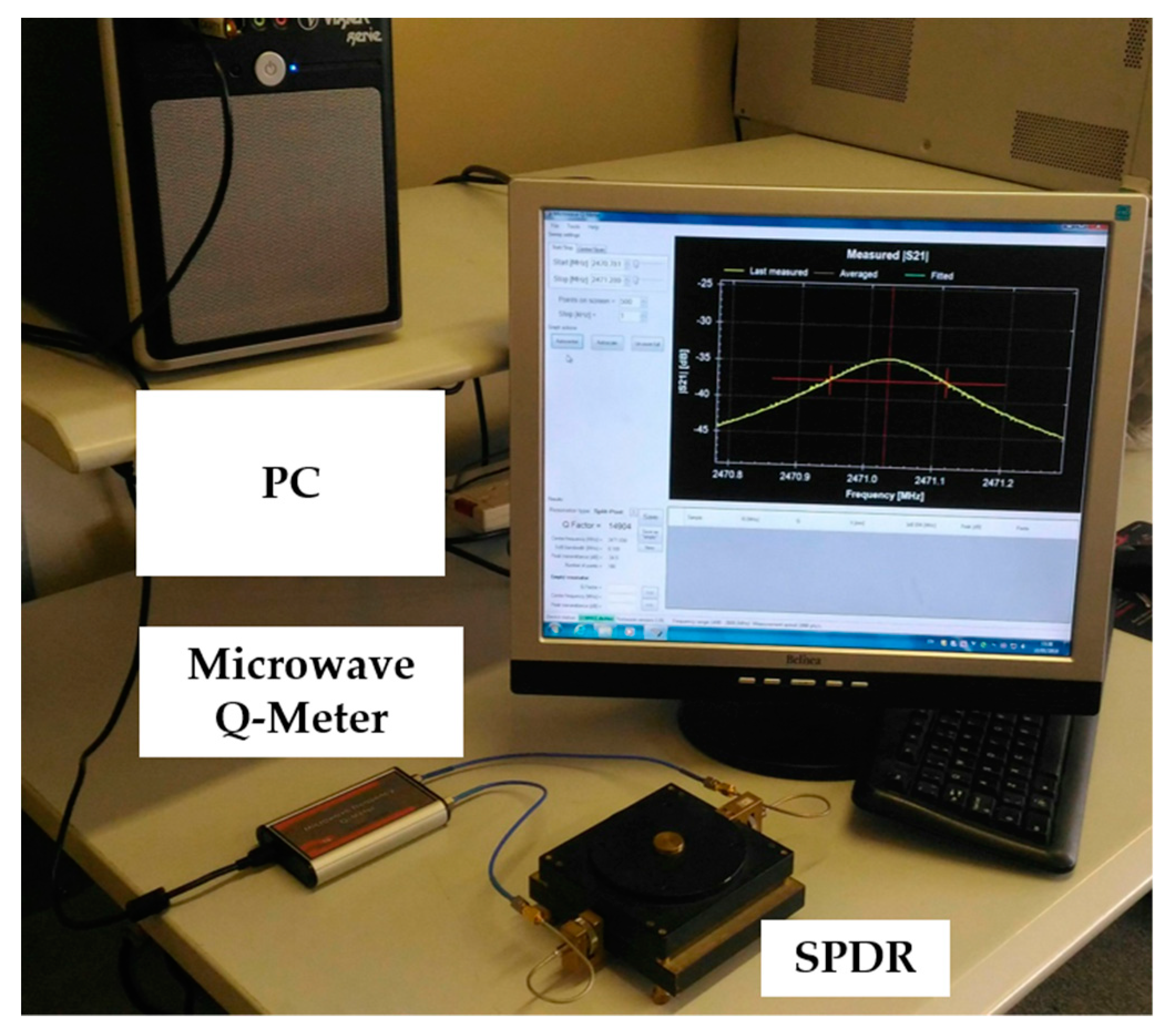
3.1. Split Post Dielectric Resonator (SPDR)
- h is the thickness of the MUT;
- is the resonant frequency of the empty SPDR;
- is the resonant frequency of the SPDR with MUT;
- is a function of and h, and has been evaluated for a number of and h using the Rayleigh–Ritz technique. For a practical approach, a number of and h were used for computing the exact resonant frequencies and the values of , then the whole results were tabulated.
- pes is the electric energy filling factor for the MUT;
- Q0 is the unloaded Q-factor of the resonator with MUT;
- QDR is the Q-factor depending on dielectric losses of the empty resonator;
- is the Q-factor depending on metal enclosure losses of the empty resonator.
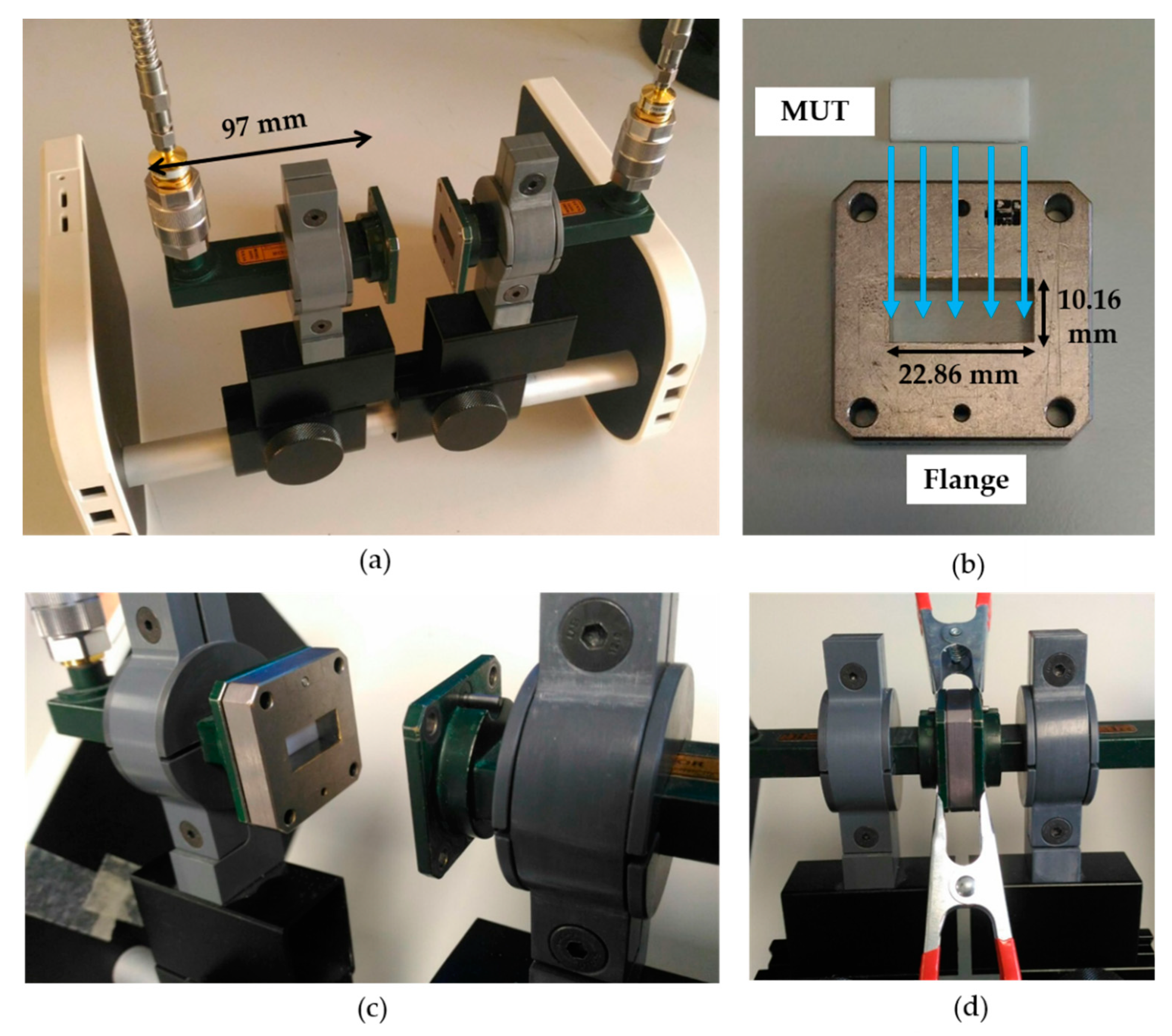
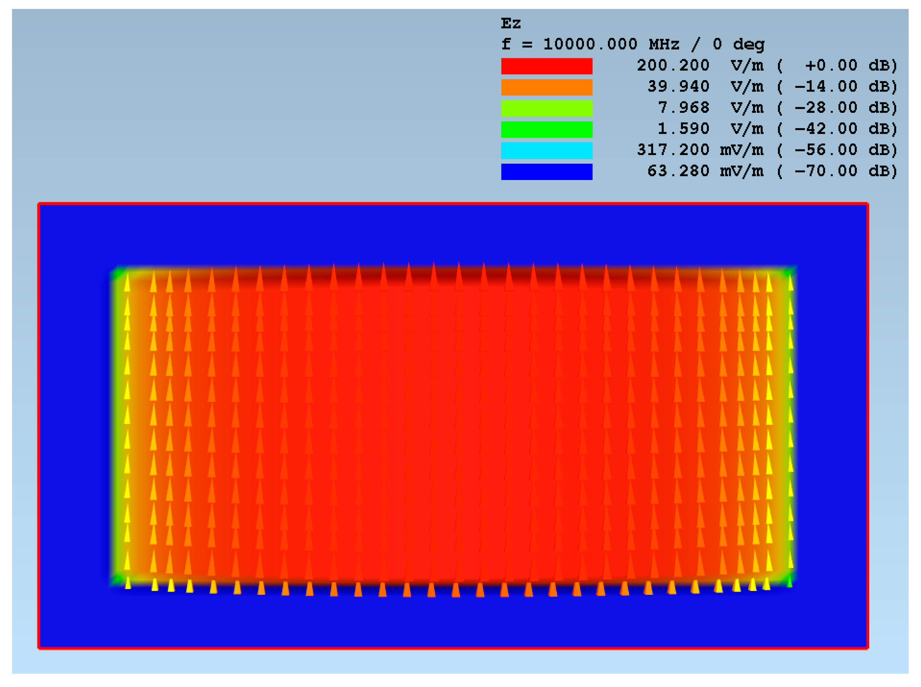
3.2. Rectangular Waveguide
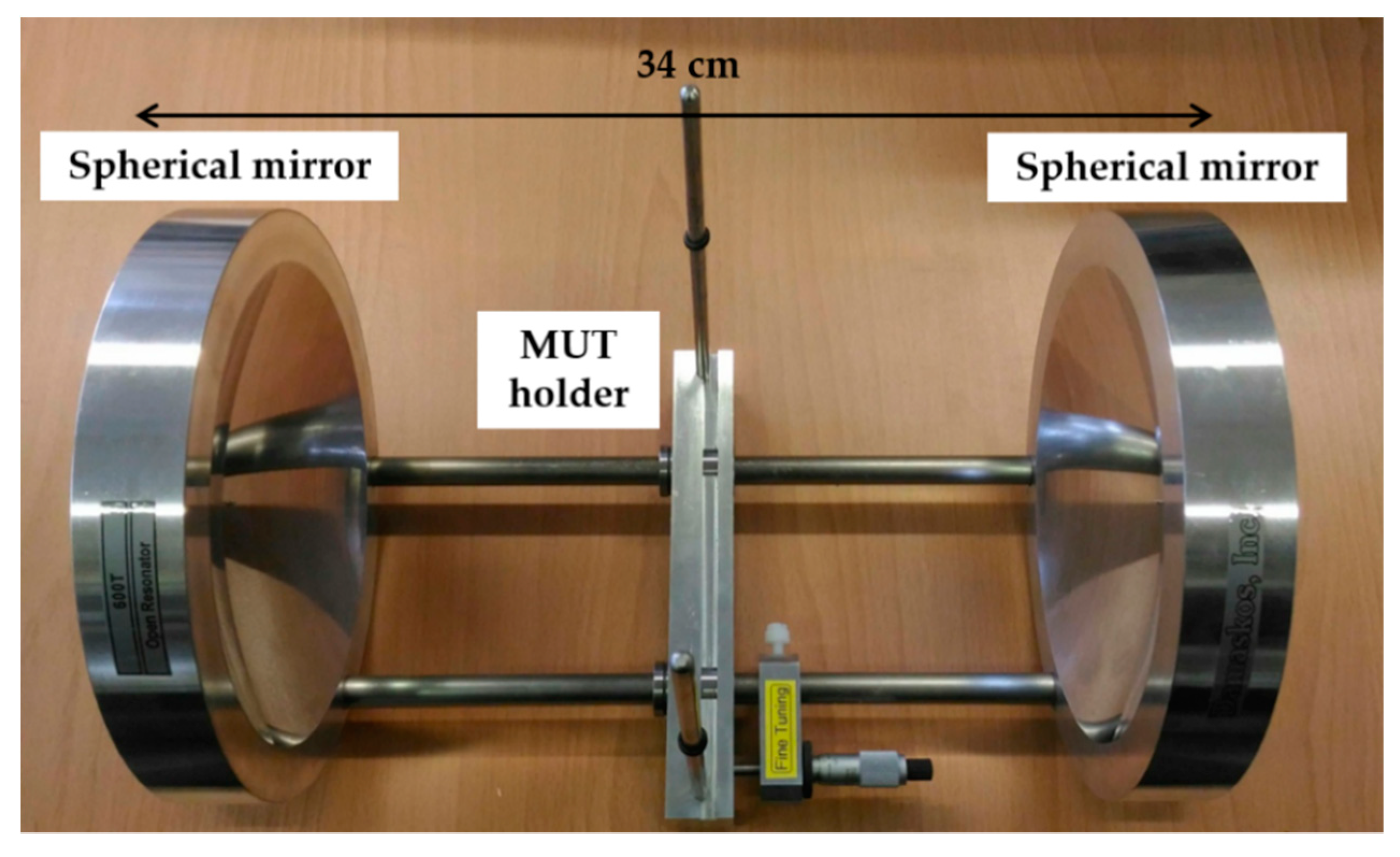
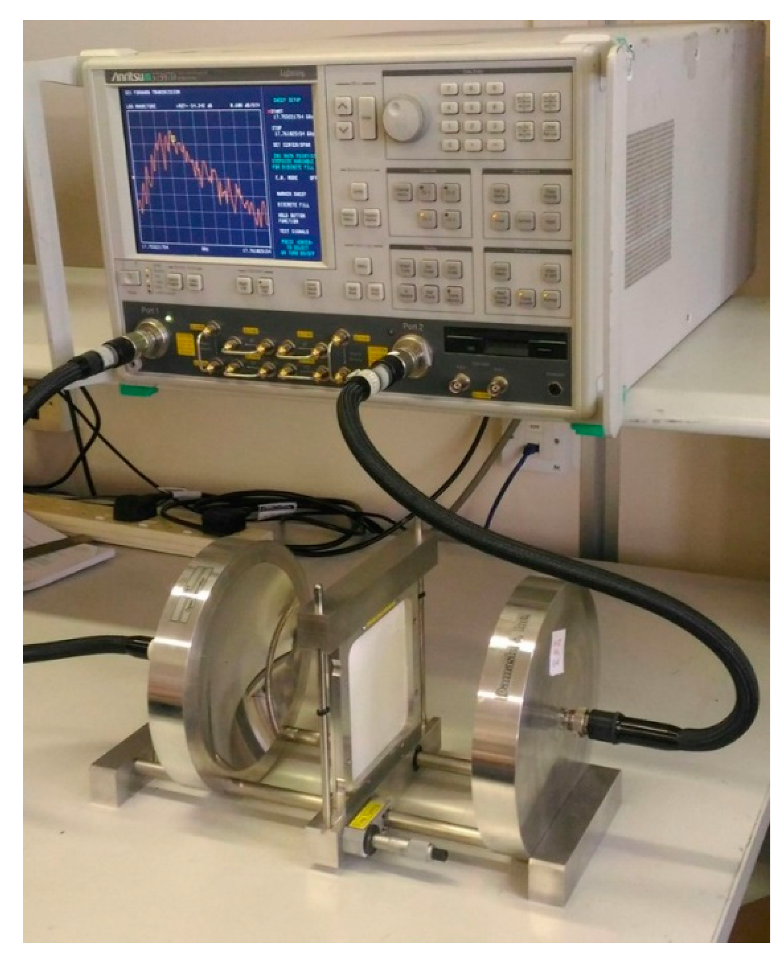
3.3. Open Resonator: Model 600T from Damaskos, Inc.
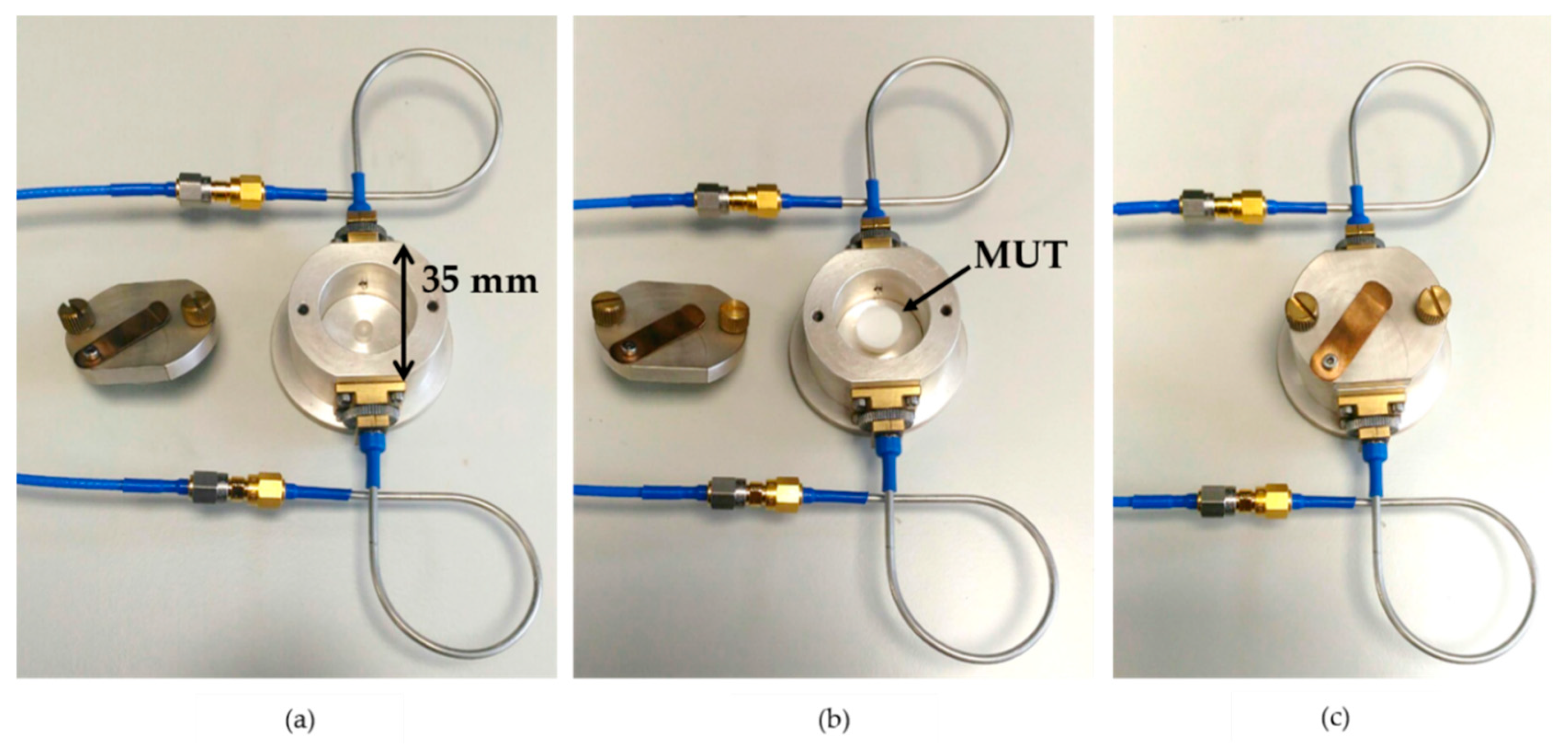
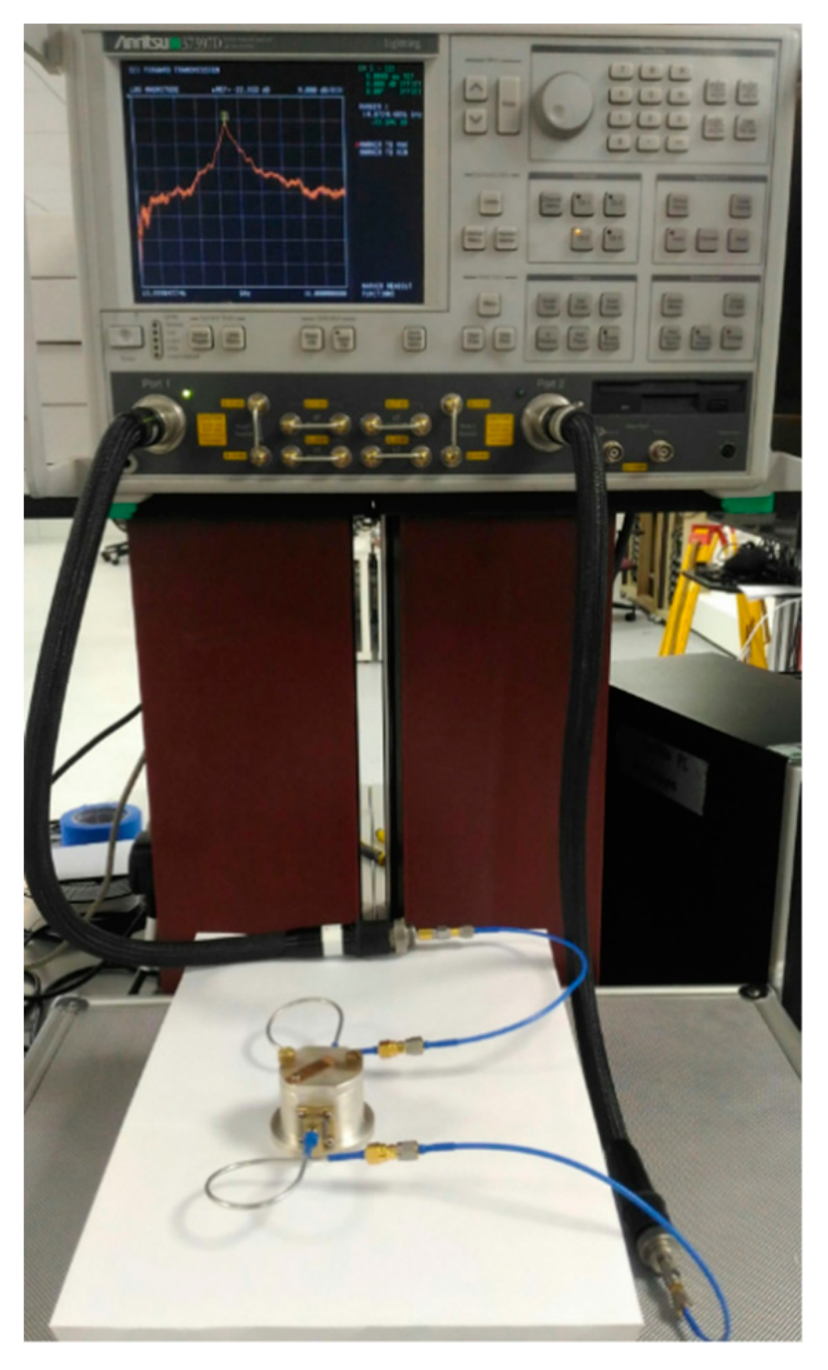
3.4. Cavity Resonator: TE01δ Mode Dielectric Resonator
3.5. Summary of Commercial Methods for Characterization
4. 3D-Printed MUTs and Measurement Results
5. Conclusions
Author Contributions
Funding
Conflicts of Interest
References
- American Society for Testing & Materials. Standard Terminology for Additive Manufacturing Technologies; ASTM International: West Conshohocken, PA, USA, 2012. [Google Scholar]
- Franchetti, M.; Kress, C. An economic analysis comparing the cost feasibility of replacing injection molding processes with emerging additive manufacturing techniques. Int. J. Adv. Manuf. Technol. 2017, 88, 2573–2579. [Google Scholar] [CrossRef]
- Deffenbaugh, P.I.; Rumpf, R.C.; Church, K.H. Broadband microwave frequency characterization of 3-D printed materials. IEEE Trans. Compon. Packag. Manuf. Technol. 2013, 3, 2147–2155. [Google Scholar] [CrossRef]
- Deffenbaugh, P.I.; Weller, T.M.; Church, K.H. Fabrication and Microwave Characterization of 3-D Printed Transmission Lines. IEEE Microw. Wirel. Components Lett. 2015, 25, 823–825. [Google Scholar] [CrossRef]
- Bukhari, S.S.; Whittow, W.G.; Zhang, S.; Vardaxoglou, J.C. Composite materials for microwave devices using additive manufacturing. Electron. Lett. 2016, 52, 832–833. [Google Scholar] [CrossRef] [Green Version]
- Motevasselian, A.; Whittow, W.G. Miniaturization of a circular patch microstrip antenna using an arc projection. IEEE Antennas Wirel. Propag. Lett. 2017, 16, 517–520. [Google Scholar] [CrossRef]
- Zhang, S.; Njoku, C.C.; Whittow, W.G.; Vardaxoglou, J.C. Novel 3D printed synthetic dielectric substrates. Microw. Opt. Technol. Lett. 2015, 57, 2344–2346. [Google Scholar] [CrossRef] [Green Version]
- Whittow, W.G.; Bukhari, S.S.; Jones, L.A.; Morrow, I.L. Applications and future prospects for microstrip antennas using heterogeneous and complex 3-D geometry substrates. Prog. Electromagn. Res. 2014, 144, 271–280. [Google Scholar] [CrossRef]
- Zhang, S.; Whittow, W.; Vardaxoglou, J.; Yiannis, C. Additively manufactured artificial materials with metallic meta-atoms. IET Microw. Antennas Propag. 2017, 11, 1955–1961. [Google Scholar] [CrossRef]
- Zhang, S.; Arya, R.K.; Pandey, S.; Vardaxoglou, Y.; Whittow, W.; Mittra, R. 3D-printed planar graded index lenses. IET Microw. Antennas Propag. 2016, 10, 1411–1419. [Google Scholar] [CrossRef]
- Agilent Technologies Inc. Agilent Network Analyzer Basics. Available online: Anlage.umd.edu/.../Agilent NWA Basics 5965-7917E.pdf%0A%0A (accessed on 30 June 2019).
- National Instruments Introduction to network analyzer measurements. Available online: download.ni.com/evaluation/rf/Introduction_to_Network_Analyzer_Measurements.pdf (accessed on 24 September 2019).
- Chen, L.F.; Ong, C.K.; Neo, C.P.; Varadan, V.V.; Varadan, V.K. Measurement and Materials Characterization; John Wiley & Sons, Inc.: Chichester, UK, 2004. [Google Scholar]
- Rohde&Schwarz Measurement of Dielectric Material Properties Application Note. Available online: https://www.rohde-schwarz.com/file/RAC-0607-0019_1_5E.pdf (accessed on 30 June 2019).
- Nicolson, A.M.; Ross, G.F. Measurement of the intrinsic properties of materials by time-domain techniques. IEEE Trans. Instrum. Meas. 1970, 19, 377–382. [Google Scholar] [CrossRef]
- Weir, W.B. Automatic measurement of complex dielectric constant and permeability at microwave frequencies. Proc. IEEE 1974, 62, 33–36. [Google Scholar] [CrossRef]
- Ghodgaonkar, D.K.; Varadan, V.V.; Varadan, V.K. A Free-Space Method for Measurement of Dielectric Constants and Loss Tangents at Microwave Frequencies. IEEE Trans. Instrum. Meas. 1989, 38, 789–793. [Google Scholar] [CrossRef]
- Sheen, J. Study of microwave dielectric properties measurements by various resonance techniques. Meas. Sci. Technol. 2009, 20, 123–130. [Google Scholar] [CrossRef]
- Hakki, B.W.; Coleman, P.D. A dielectric resonator method of measuring inductive capacities in the millimeter range. IRE Trans. Microw. Theory Tech. 1960, 8, 402–410. [Google Scholar] [CrossRef]
- Courtney, W.E. Analysis and evaluation of a method of measuring the complex permittivity and permeability microwave insulators. IEEE Trans. Microw. Theory Tech. 1970, 18, 476–485. [Google Scholar] [CrossRef]
- Waldron, R.A. Perturbation theory of resonant cavities. Proc. IEE Part C Monogr. 1960, 107, 272–274. [Google Scholar] [CrossRef]
- Dube, D.C.; Lanagan, M.T.; Kim, J.H.; Jang, S.J. Dielectric measurements on substrate materials at microwave frequencies using a cavity perturbation technique. J. Appl. Phys. 1988, 63, 2466–2468. [Google Scholar] [CrossRef]
- Waldron, R.A. Perturbation formulas for elastic resonators and waveguides. IEEE Trans. Sonics Ultrason. 1971, 18, 16–20. [Google Scholar] [CrossRef]
- Nishikawa, T.; Wakino, K.; Tanaka, H.; Ishikawa, Y. Precise measurement method for complex permittivity of microwave dielectric substrate. In Proceedings of the 1988 Conference on Precision Electromagnetic Measurements, Ibaraki, Japan, 7–10 June 1988; Volume 9, pp. 155–156. [Google Scholar]
- Krupka, J.; Geyer, R.G.; Baker-Jarvis, J.; Ceremuga, J. Measurements of the complex permittivity of microwave circuit board substrates using split dielectric resonator and reentrant cavity techniques. In Proceedings of the Seventh International Conference on Dielectric Materials Measurements &Applications, Bath, UK, 23–26 September 1996; pp. 21–24. [Google Scholar]
- Krupka, J.; Clarke, R.N.; Rochard, O.C.; Gregory, A.P. Split post dielectric resonator technique for precise measurements of laminar dielectric specimens-measurement uncertainties. In Proceedings of the 13th International Conference on Microwaves, Radar and Wireless Communications, Wroclaw, Poland, 22–24 May 2000; pp. 305–308. [Google Scholar]
- Dziurdzia, B.; Krupka, J.; Gregorczyk, W. Characterization of thick-film dielectric at microwave frequencies. In Proceedings of the International Conference on Microwaves, Radar & Wireless Communications, Krakow, Poland, 22–24 May 2006; pp. 361–364. [Google Scholar]
- Jacob, M.; Krupka, J.; Derzakowski, K.; Mazierska, J. Measurements of thin polymer films employing split post dielectric resonator technique. In Proceedings of the International Conference on Microwaves, Radar & Wireless Communications, Krakow, Poland, 22–24 May 2006; pp. 229–231. [Google Scholar]
- Krupka, J.; Jacob, M.; Givot, B.; Derzakowski, K. Measurements of thin resistive films employing split post dielectric resonator technique. In Proceedings of the 17th International Conference on Microwaves, Radar and Wireless Communications, Wroclaw, Poland, 19–21 May 2008; pp. 1–4. [Google Scholar]
- Chen, F.; Mao, S.; Wang, X.; Semouchkina, E.; Lanagan, M. Effects of cavity dimensions in split-post dielectric resonator technique for complex permittivity measurements. In Proceedings of the IEEE International Symposium on Antennas and Propagation, Chicago, IL, USA, 8–14 July 2012; pp. 1–2. [Google Scholar]
- Korpas, P.; Wojtasiak, W.; Krupka, J.; Gwarek, W. Inexpensive approach to dielectric measurements. In Proceedings of the 19th International Conference on Microwaves, Radar and Wireless Communications, Warsaw, Poland, 21–23 May 2012; pp. 154–157. [Google Scholar]
- QWED Company Split Post Dielectric Resonators (SPDR). Available online: http://www.qwed.com.pl/resonators_spdr.html (accessed on 30 June 2019).
- Treacy, E.B. The two-cone open resonator. Proc. IEEE 1966, 54, 555–560. [Google Scholar] [CrossRef]
- Yu, P.K. Measurements Using an Open Resonator; University College London: London, UK, 1970. [Google Scholar]
- Cullen, A.L.; Yu, P.K. The accurate measurement of permittivity by means of an open resonator. Proc. R. Soc. Lond. 1971, 325, 493–509. [Google Scholar] [CrossRef]
- Yu, P.K.; Cullen, A.L. Measurement of permittivity by means of an open resonator: I. Theoretical. Proc. R. Soc. Lond. 1982, 380, 49–71. [Google Scholar] [CrossRef]
- Lynch, A.C. Measurement of permittivity by means of an open resonator: I. Experimental. Proc. R. Soc. Lond. 1982, 380, 73–76. [Google Scholar] [CrossRef]
- Cullen, A.L.; Nagenthiram, P.N.; Williams, A.D. A variational approach to the theory of the open resonator. Proc. R. Soc. Lond. 1972, 329, 153–169. [Google Scholar] [CrossRef]
- Cook, R.J.; Jones, R.G. Correction to open resonator permittivity and loss measurements. Electron. Lett. 1976, 12, 1–2. [Google Scholar] [CrossRef]
- Di Massa, G.; Cuomo, D.; Cutolo, A.; Cave, G.D. Open resonator for microwave application. IEE Proc. H Microw. Antennas Propag. 1989, 136, 159–164. [Google Scholar] [CrossRef]
- Mongia, R.K.; Arora, R.K. Accurate measurement of the Q factor of an open resonator in the W-band frequency range of an open resonator. Am. Inst. Phys. Rev. Sci. Instrum. 1992, 63, 3877–3880. [Google Scholar] [CrossRef]
- Krupka, J.; Derzakowski, K.; Riddle, B.; Baker-Jarvis, J. A dielectric resonator for measurements of complex permittivity of low loss dielectric materials as a function of temperature. Meas. Sci. Technol. 1998, 9, 1751–1756. [Google Scholar] [CrossRef]
- Ford, S.; Despeisse, M. Additive manufacturing and sustainability: An exploratory study of the advantages and challenges. J. Clean. Prod. 2016, 137, 1573–1587. [Google Scholar] [CrossRef]
- Tymrak, B.M.; Kreiger, M.; Pearce, J.M. Mechanical properties of components fabricated with open-source 3-D printers under realistic environmental conditions. Mater. Des. 2014, 58, 242–246. [Google Scholar] [CrossRef]
- Jerez-Mesa, R.; Travieso-Rodriguez, J.A.; Llumà-Fuentes, J.; Gomez-Gras, G.; Puig, D. Fatigue lifespan study of PLA parts obtained by additive manufacturing. Procedia Manuf. 2017, 13, 872–879. [Google Scholar] [CrossRef] [Green Version]
- Cicala, G.; Giordano, D.; Tosto, C.; Filippone, G.; Recca, A.; Blanco, I. Polylactide (PLA) filaments a biobased solution for additive manufacturing: Correlating rheology and thermomechanical properties with printing quality. Materials 2018, 11, 1191. [Google Scholar] [CrossRef] [PubMed]
- Riddle, B.; Baker-Jarvis, J.; Krupka, J. Complex permittivity measurements of common plastics over variable temperatures. IEEE Trans. Microw. Theory Tech. 2003, 51, 727–733. [Google Scholar] [CrossRef]
- Malek, N.F.A.; Ramly, A.M.; Sidek, A.A.; Yusri, M.S. Characterization of acrylonitrile butadiene styrene for 3D printed patch antenna. Indones. J. Electr. Eng. Comput. Sci. 2017, 6, 116–123. [Google Scholar] [CrossRef]
- Shinyama, K.; Fujita, S. Study on the electrical properties of a biodegradable plastic. In Proceedings of the Proceedings of the 7th International Conference on Properties and Applications of Dielectric Materials (Cat. No.03CH37417), Nagoya, Japan, 1–5 June 2003; Volume 2, pp. 707–710. [Google Scholar]
- Hernandez, D.D. Factors affecting dimensional precision of consumer 3D printing. Int. J. Aviat. Aeronaut. Aerosp. 2015, 2, 2. [Google Scholar] [CrossRef]


| Frequency (GHz) | Minimum Size (mm × mm) | Maximum Width (mm) | Maximum Thickness (mm) |
|---|---|---|---|
| 1.1 | 120 × 120 | 150 | 6.0 |
| 1.9 | 70 × 70 | 100 | 4.1 |
| 2.4 | 55 × 55 | 100 | 3.1 |
| Method | MUT Shape | Minimum Size (mm × mm) | Maximum Size (mm × mm) | Maximum Thickness (mm) |
|---|---|---|---|---|
| SPDR | rectangular | 120 × 120 | Any × 150 | 6.0 |
| SPDR | rectangular | 70 × 70 | Any × 100 | 4.1 |
| SPDR | rectangular | 55 × 55 | Any × 100 | 3.1 |
| X-band waveguide | rectangular | 22.86 × 10.16 | 22.86 × 10.16 | Sample-dependent |
| Damaskos model 600T open resonator | square | 120 × 120 | 120 × 120 | 50 |
| TE01δ cavity resonator | cylinder | Diameter: 6 (12 for low εr samples) Height: 3 | Diameter: 16 Height: 6 | 3 |
| Method | Class | Frequency (GHz) | Calibration Time (min) | Measurement Time (min) |
|---|---|---|---|---|
| SPDR | Resonant perturbation | 1.1, 1.9, 2.4 | No need | Less than 1 |
| X-band waveguide | Transmission/reflection | 8.2 to 12.4 | 3 | Less than 1 |
| Damaskos model 600T open resonator | Resonator | 10 to 70 | 20 | More than 10 |
| TE01δ cavity resonator | Resonator | Sample-dependent | No need | Less than 1 |
| Material | Initial Layer Height (mm) | Layer Height (mm) | Print Temp. (°C) | Bed Temp. (°C) | Print Speed (mm/s) | Infill (%) | Infill Angle (°) | Shells |
|---|---|---|---|---|---|---|---|---|
| ABS | 0.3 | 0.2 | 250 | 110 | 60 | 100 | 45 | 2 |
| PLA | 0.3 | 0.2 | 220 | 60 | 80 | 100 | 45 | 2 |
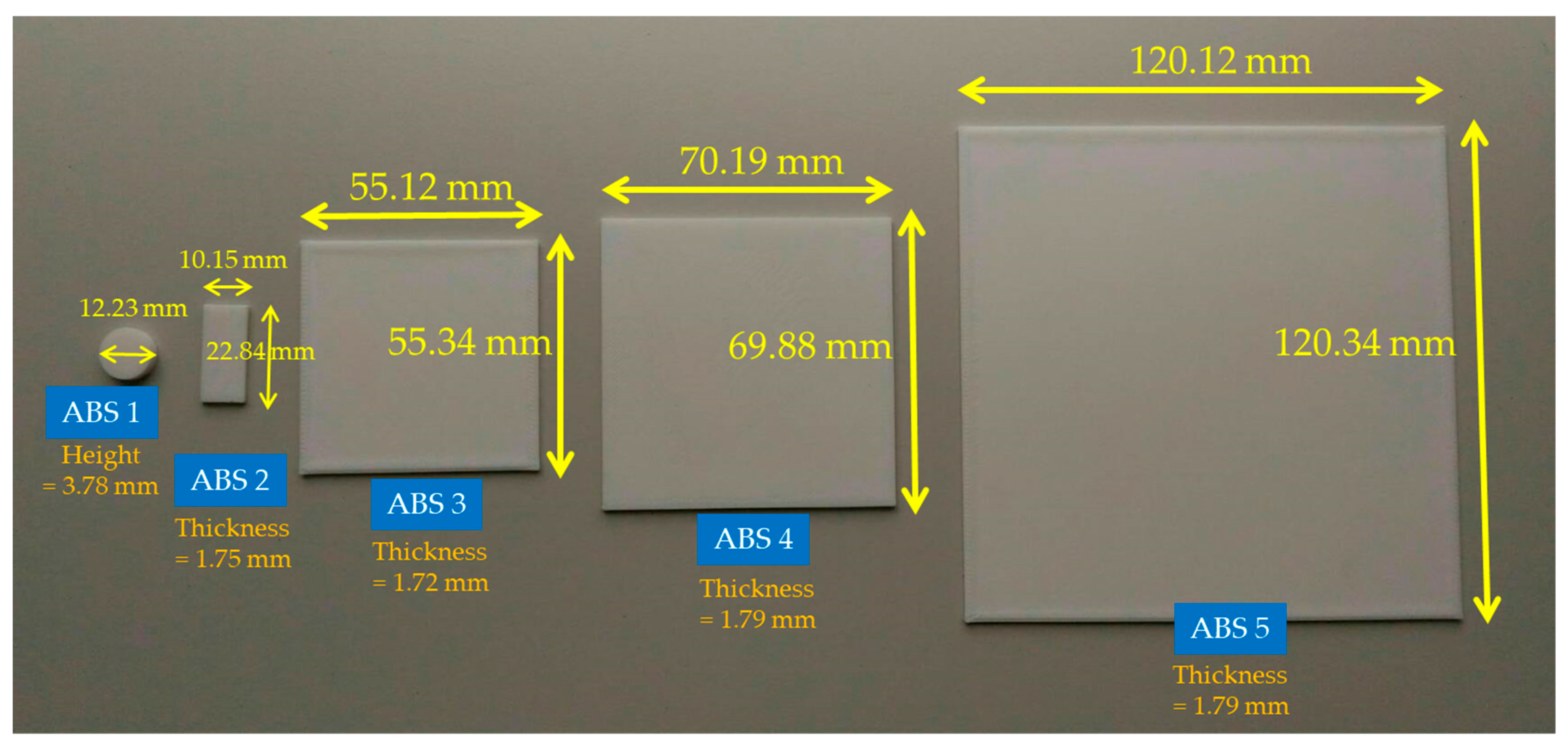
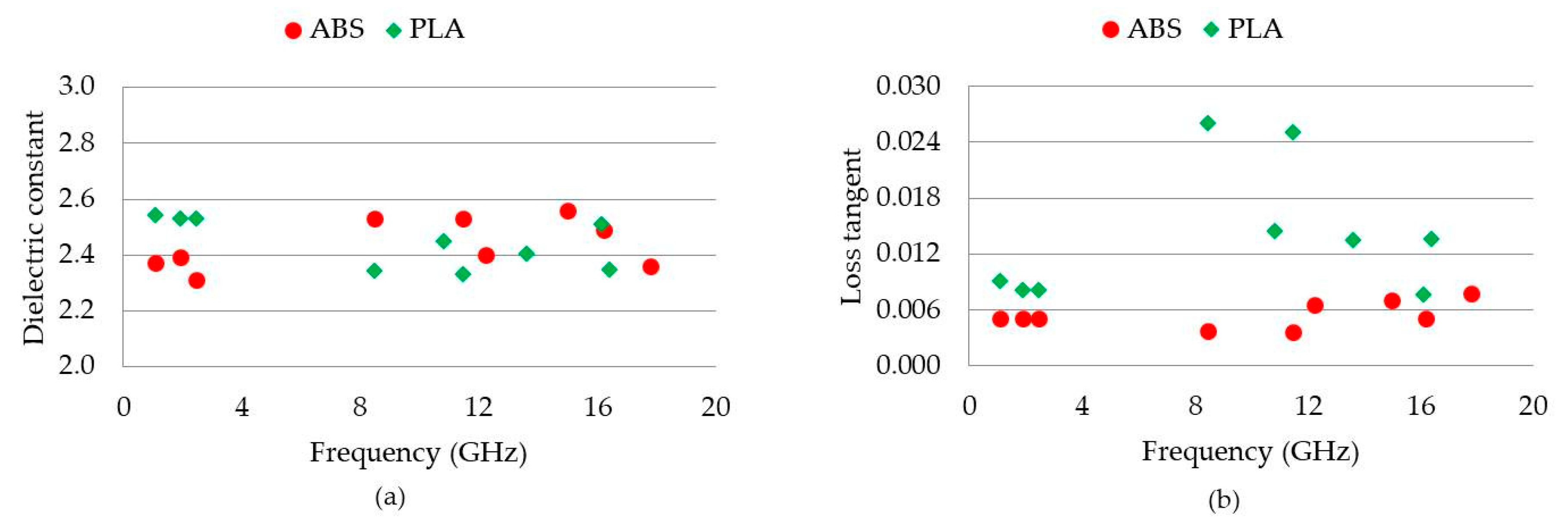
| MUT | Fabricated Size (mm) | Measurement Method | Frequency (GHz) | Dielectric Constant | Loss Tangent |
|---|---|---|---|---|---|
| ABS 1 | Diameter: 12.23 Height: 3.78 | TE01δ mode cavity resonator | 16.2 | 2.49 | 0.005 |
| ABS 2 | 22.84 × 10.15 × 1.75 | X-band waveguide | 8.2 to 12.4 | 2.53 (mean) | 0.004 (mean) |
| ABS 3 | 55.12 × 55.34 × 1.72 | SPDR | 2.4 | 2.31 | 0.005 |
| ABS 4 | 70.19 × 69.88 × 1.79 | SPDR | 1.9 | 2.39 | 0.005 |
| ABS 5 | 120.12 × 120.34 × 1.79 | SPDR | 1.1 | 2.37 | 0.005 |
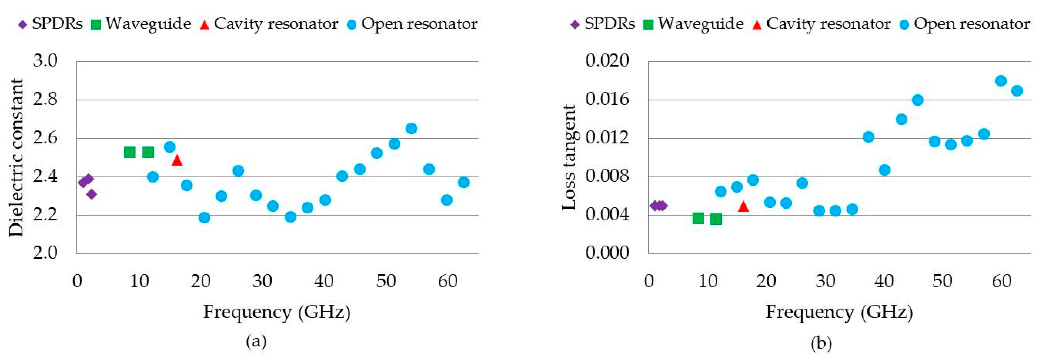
| Open resonator | 12.3 to 62.6 | 2.37 (mean) | 0.009 (mean) |
| MUT | Fabricated Size (mm) | Measurement Method | Frequency (GHz) | Dielectric Constant | Loss Tangent |
|---|---|---|---|---|---|
| PLA 1 | Diameter: 12.11 Height: 3.83 | TE01δ mode cavity resonator | 16.1 | 2.51 | 0.008 |
| PLA 2 | 22.82 × 10.12 × 1.74 | X-band waveguide | 8.2 to 12.4 | 2.52 (mean) | 0.022 (mean) |
| PLA 3 | 55.23 × 55.11 × 1.53 | SPDR | 2.4 | 2.53 | 0.009 |
| PLA 4 | 69.89 × 70.33 × 1.56 | SPDR | 1.9 | 2.54 | 0.008 |
| PLA 5 | 120.12 × 120.41 × 1.59 | SPDR | 1.1 | 2.61 | 0.009 |
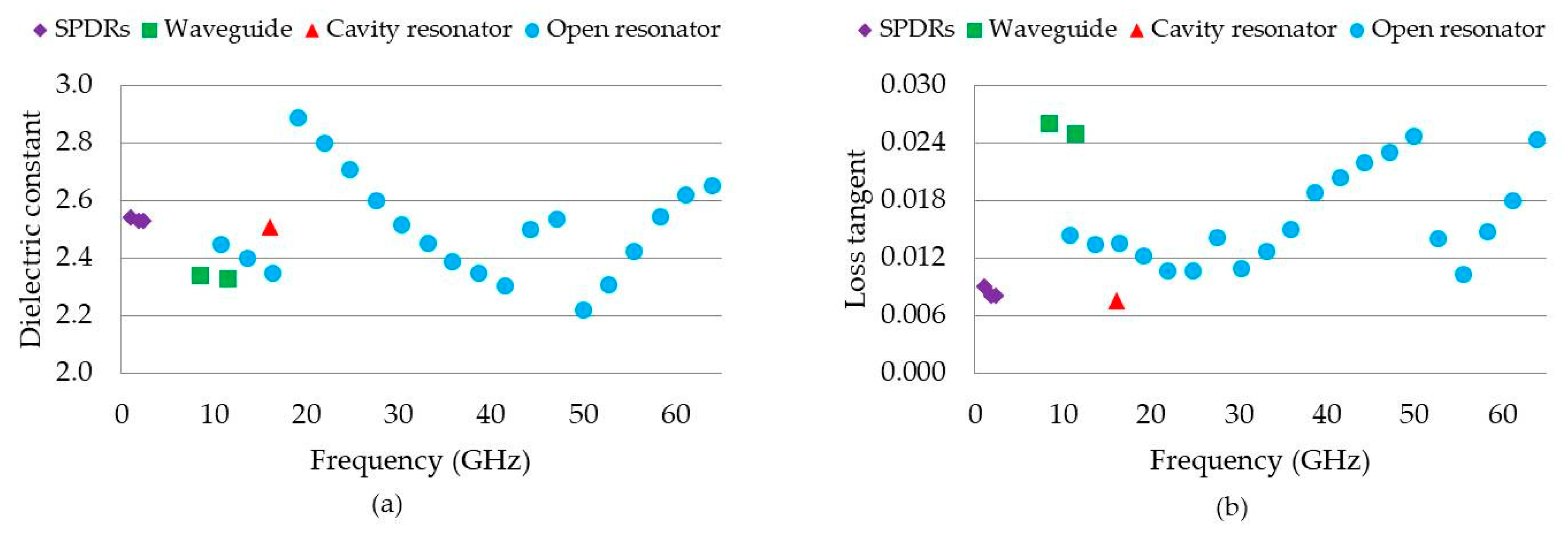
| Open resonator | 10.8 to 63.9 | 2.55 (mean) | 0.016 (mean) |
© 2019 by the authors. Licensee MDPI, Basel, Switzerland. This article is an open access article distributed under the terms and conditions of the Creative Commons Attribution (CC BY) license (http://creativecommons.org/licenses/by/4.0/).
Share and Cite
Lee, C.-K.; McGhee, J.; Tsipogiannis, C.; Zhang, S.; Cadman, D.; Goulas, A.; Whittaker, T.; Gheisari, R.; Engstrom, D.; Vardaxoglou, J.; et al. Evaluation of Microwave Characterization Methods for Additively Manufactured Materials. Designs 2019, 3, 47. https://0-doi-org.brum.beds.ac.uk/10.3390/designs3040047
Lee C-K, McGhee J, Tsipogiannis C, Zhang S, Cadman D, Goulas A, Whittaker T, Gheisari R, Engstrom D, Vardaxoglou J, et al. Evaluation of Microwave Characterization Methods for Additively Manufactured Materials. Designs. 2019; 3(4):47. https://0-doi-org.brum.beds.ac.uk/10.3390/designs3040047
Chicago/Turabian StyleLee, Chih-Kuo, Jack McGhee, Christos Tsipogiannis, Shiyu Zhang, Darren Cadman, Athanasios Goulas, Tom Whittaker, Reza Gheisari, Daniel Engstrom, John (Yiannis) Vardaxoglou, and et al. 2019. "Evaluation of Microwave Characterization Methods for Additively Manufactured Materials" Designs 3, no. 4: 47. https://0-doi-org.brum.beds.ac.uk/10.3390/designs3040047