Article

Permittivity of 3D-Printed Nylon Substrates with Different Infill Patterns and Densities for Design of Microwave Components

1
School of Electrical Engineering and Computer Science, The Pennsylvania State University, University Park, PA 16802, USA
2
Department of Mechanical Engineering, The Pennsylvania State University, University Park, PA 16802, USA
3
School of Engineering Design, Technology, and Professional Programs, The Pennsylvania State University, University Park, PA 16802, USA
*
Author to whom correspondence should be addressed.
Submission received: 11 August 2020 / Revised: 4 September 2020 / Accepted: 11 September 2020 / Published: 18 September 2020

Abstract

:
Printed circuit boards, chemical etching, and computer numerical control milling currently dominate industrial processes for manufacturing microwave components. However, these manufacturing methods do not provide the flexibility for customization possible with additive manufacturing. Additive manufacturing (AM) has the potential to fabricate microwave components for desired frequency ranges with less effort in prototyping and fabrication. Relative permittivity ( ε r ) of materials is a critical parameter in microwave component design, yet the value changes during the AM process. This article investigates how relative permittivity for nylon substrates, created with AM, changes with different infill densities and infill patterns. The measurement method and procedure can be used to design AM microwave components like antennas or dielectric-filled waveguides with desired characteristics. The two-microstrip-line method was used and improved for the accurate and convenient measurement of the relative permittivity of AM nylon substrates. Several nylon substrates with different infill patterns, including rectangular, hexagonal, triangular, and solid, were fabricated with AM to demonstrate how the relative permittivity value changes as the infill density increases. A linear relationship between the infill density of the rectangular pattern and the substrate permittivity was found. The permittivity data were applied to the design of a rectangular patch antenna for use in the 2.5-GHz WiMAX band. The fabricated antenna with AM, which was tested using a vector network analyzer, showed good agreement with simulation results. The method and procedure of permittivity measurements are specially designed to be applied in the design of microwave components with AM dielectric substrates.

1. Introduction

Additive manufacturing, often referred to as 3D printing, builds geometrically complex objects from a series of layers, each “printed” on top of the previous one. Significant research and press have recently focused on how AM can create both prototypes and end-use products [1,2]. The flexibility of AM technology allows design modifications to be immediately implemented, enabling new paradigms within the manufacturing process. One unique advantage offered by AM is the fact that it provides users with access to every point of the part’s volume during manufacturing. This advantage enables the possibility of incorporating functional components, such as electronics, during the process of a build operation [3,4]. However, multifunctional AM is still in its relative infancy; for the technology to be universally adopted for direct product manufacturing, a better understanding of multifunctional material properties created with AM is required.
By taking advantage of AM, customized parts integrated with more functions have been manufactured with a high degree of design freedom at a low cost [5,6]. For example, significant research is underway in the area of manufacturing microwave components using AM. A wide variety of these components, such as switched-line phase shifters [7], distributed impedance elements [8], and transmission lines [9] have already been fabricated by AM. Many antennas for high frequency applications have also been fabricated using AM processes, such as material extrusion, material jetting, and micro dispensing [10,11,12]. To fabricate microwave components by AM, direct print technology using conductive inks with low processing temperatures are reported [13], and they can be easily and accurately dispensed on dielectric substrates. Nonplanar geometries include a spiral dipole antenna working at frequencies from 1 GHz to 10 GHz embedded in polycarbonate [14]. AM technology is becoming more capable of fabricating microwave components with more complex structures over a wider frequency range. However, AM materials differ from bulk manufactured materials due to deposition of material by a point nozzle, which makes AM parts susceptible to air gaps [15,16]. In most cases, researchers have not addressed print parameters such as different infill densities or material properties.
Properties of AM material tend to change with the AM build process, especially the permittivity. Permittivity describes how easily a material polarizes in response to an electric field, and it is one of the key parameters in designing microwave components as it affects the size of the component. Because AM material has a higher permittivity than air, it shrinks the wavelength of the signal propagating through it [17], and therefore the wavelength in AM substrates can be manipulated by carefully adjusting its design. Higher permittivity of AM materials also allows the AM microwave components to be smaller than conventional microwave components. In light of this, to design microwave components for the desired frequency range with AM, the permittivity of the structure must be obtained as a function of build parameters, since AM parts have different overall properties than the bulk material. Also, acquiring an accurate permittivity value for the dielectric material in a microwave component is crucial to ensure its efficient performance. Some of the researches have investigated the influence of changing infill density on the permittivity. To measure the permittivity, the ring-resonator technique was used for the characterization of NinjaFlex substrates with different infill densities [18,19]. The method was used to design a integrated waveguide filter [20]. However, they did not establish the relationship between the infill density and the permittivity, and fabricating a ring resonator on a NinjaFlex substrate required additional time for the ring pattern design and simulation. They also did not eliminate the deformation of the substrate under test during the measurement process.
AM dielectric materials within microwave components are usually in the form of flat thin substrates or planar shell. The permittivity of AM substrates can be affected by infill density or infill pattern. The infill serves as the internal support structure for the printed part and the infill density describes the amount of material used on the inside of the printed part. A higher infill density means that there is more material on the inside of your print, leading to a denser and stronger object. With a change in either infill density or infill pattern, different mesh structures are automatically created by software, and the volume of air present in the printed part changes, changing the effective density of the material in a part. This effective part density affects the propagation behavior of the electromagnetic wave within, defining the permittivity of the overall part, which must be accurately known during the part design process [21,22]. Therefore, to understand how infill design parameters impact the permittivity of the AM part, the following research questions were explored:

1.1. How Does Infill Density Impact the Permittivity of an AM Substrate?

Hypothesis: Since infill density directly impacts the effective material density in an AM part, the permittivity is expected to increase linearly with higher infill density.

1.2. How Does Infill Pattern Impact the Permittivity of an AM Substrate?

Hypothesis: Different infill patterns result in different material deposition paths and, therefore, different mechanical properties [23,24]. Since electrical and mechanical properties of materials are interrelated [21,25], different infill patterns are expected to exhibit different permittivity.

1.3. How Does Roof and Floor Layer Impact the Permittivity of a Solid Infill Pattern AM Substrate?

Hypothesis: The roof and floor layers are defined as solid plastic printed on the top and bottom of the part, which are denser than the infill [26]. Due to expected changes in effective density, the permittivity is expected to increase with more roof and floor layers.

2. Materials and Methods

To answer these research questions, experiments were performed on AM samples prepared with varying infill densities and infill patterns. To obtain the permittivity of AM substrates, a modification of the two-microstrip-line method was developed, making the method more suitable for measuring flexible thin AM substrates [27]. The modified method enabled the authors to determine the relative permittivity of different AM nylon substrates in less time and with less material consumption over a wide frequency range. Additionally, a functional AM patch antenna for the desired resonance frequency was simulated and fabricated to validate the applicability of the findings.

2.1. Specimen Design and Preparation

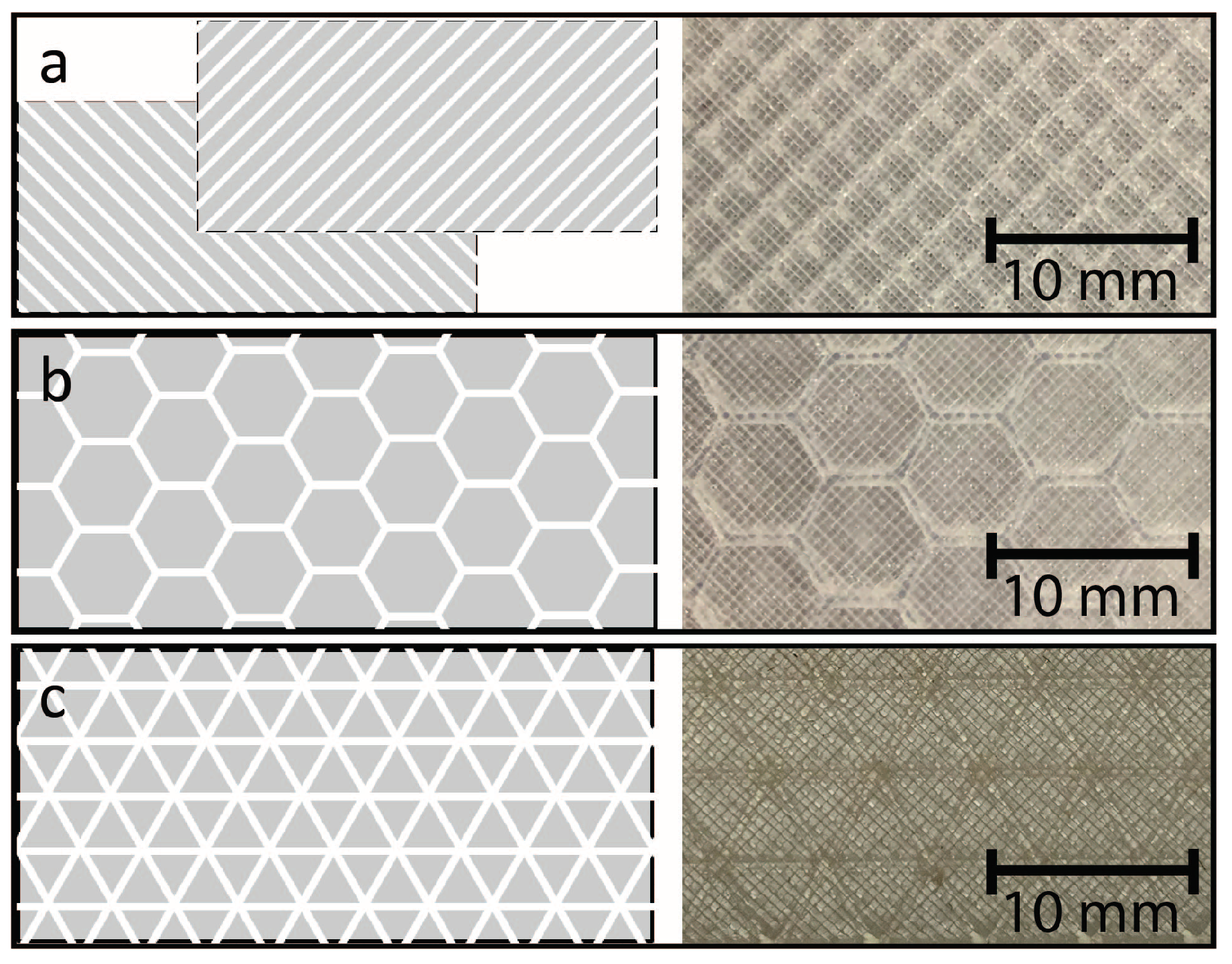
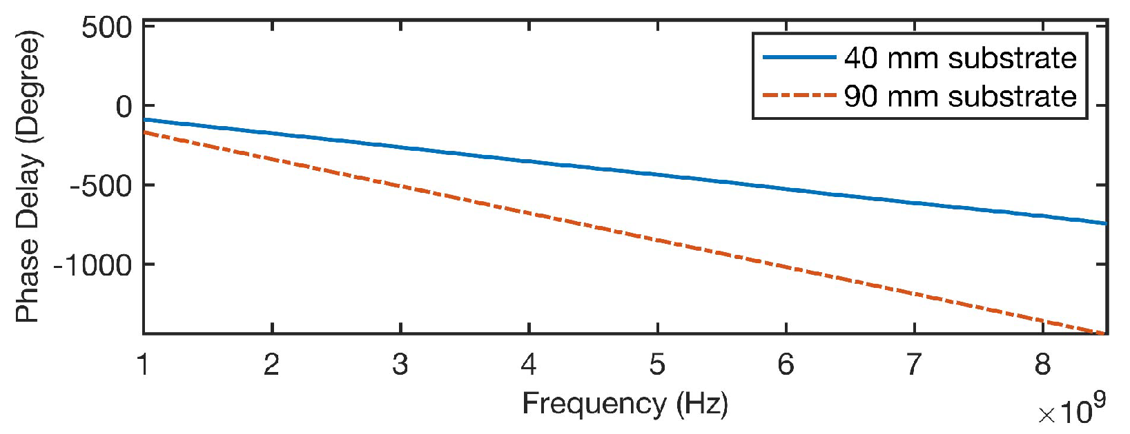
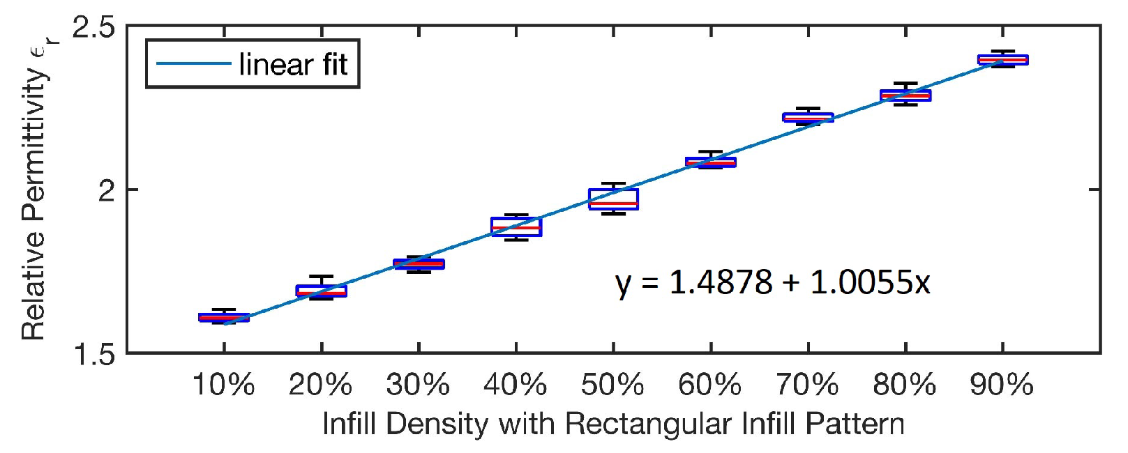
The nylon substrates were printed with different infill settings with a Markforged Mark One, a two-nozzle material extrusion AM system. Markforged Mark One is a fused deposition modeling (FDM) 3D printer that prints nylon and carbon fiber with a 0.1-mm layer resolution and a heating bed. Markforged’s cloud-based slicer “Eiger” was used to prepare the specimens and vary the settings of the printer. A pair of nylon substrates with two different dimensions were printed for each experimental setting. One was 40 × 30 × 2 mm, the other was 90 × 30 × 2 mm, with the height of 2 mm aligned perpendicular to the build plate. The difference in phase delay measurements for the two different lengths provides the data for the derivation of permittivity. All substrates were printed with a 0.1-mm layer height and a 0.8-mm shell thickness (two layers). To investigate the effect of infill density on permittivity, substrates were printed with different infill densities (ranging from 10% to 90% in increments of 10%) for a standard rectangular infill pattern (
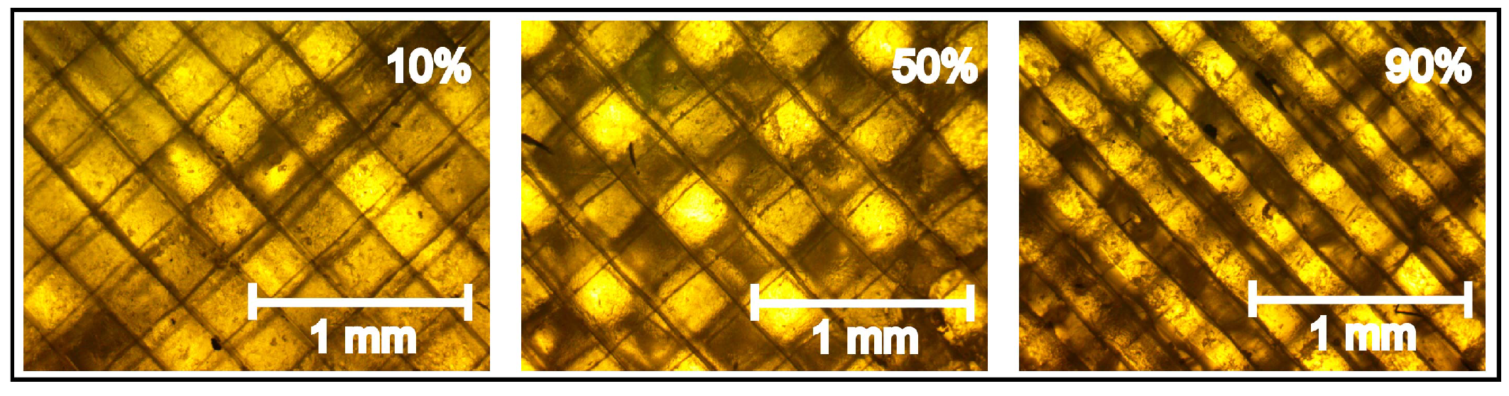
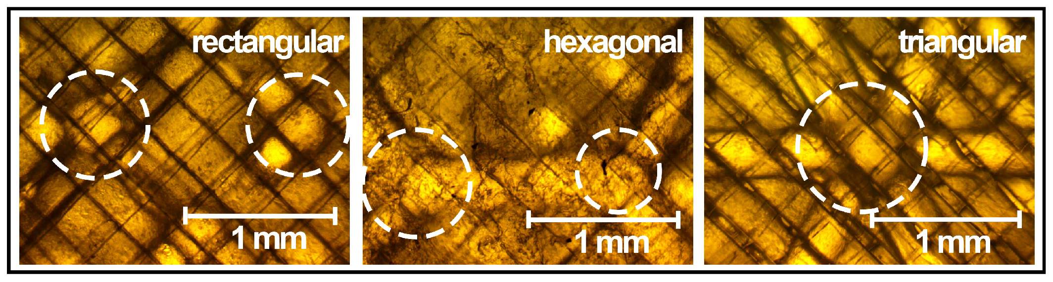
Figure 1a shows even and odd layer patterns). To investigate the effects of infill pattern on permittivity, substrates were printed with three different infill patterns: rectangular, hexagonal, and triangular (
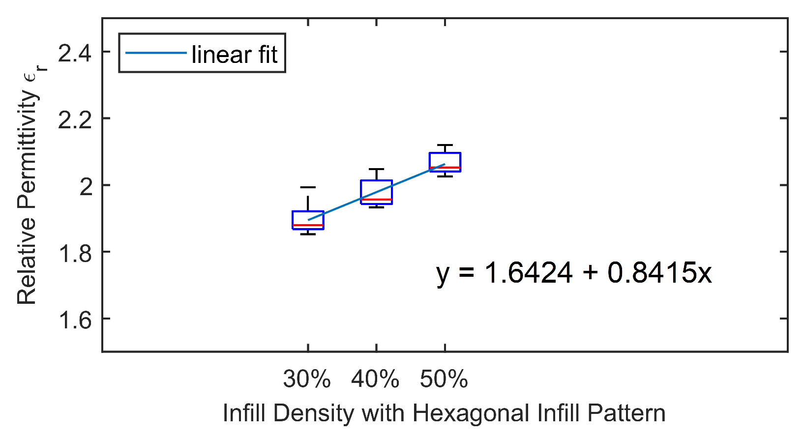
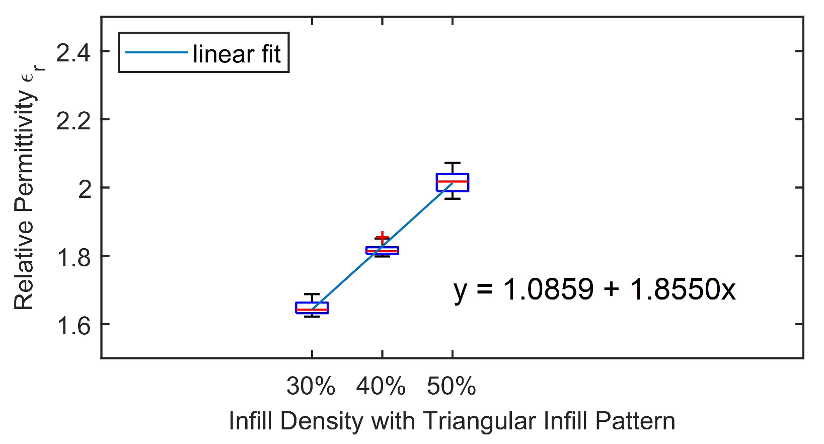
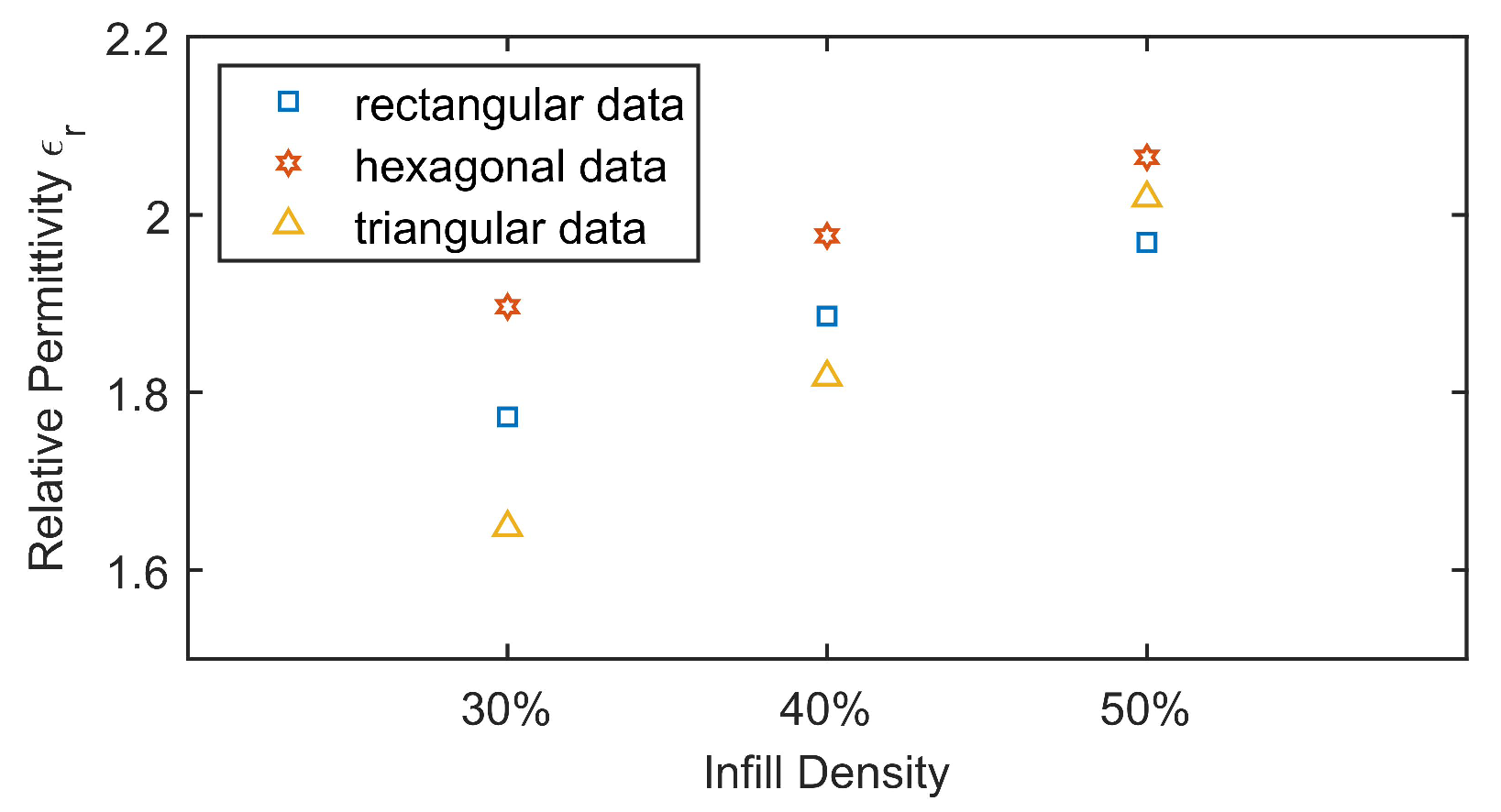
Figure 1a–c), with infill densities of 30%, 40%, and 50%. All of these specimens had four roof and floor layers, as they ensured smooth top and bottom surfaces and substrate thickness uniformity, which is essential for reliable measurements.
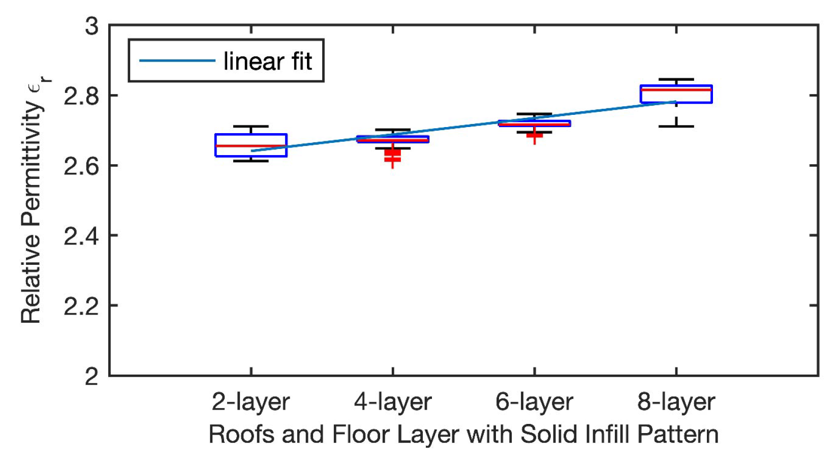
Additionally, a set of specimens with the solid infill pattern (100% dense) were printed with varying roof and floor layer numbers (2 to 8 in increments of 2). Changing the number of roof and floor layers was expected to impact the permittivity as it changed the specimen’s print time, part mass, and volume. The roof and floor layers are defined in Eiger as solid plastic layers, which are deposited such that there are no air gaps in the layer. Therefore, the effective density of the part changes in altering the number of roof and floor layers. The specimen profile obtained from Eiger is listed in Table 1, Table 2 and Table 3.
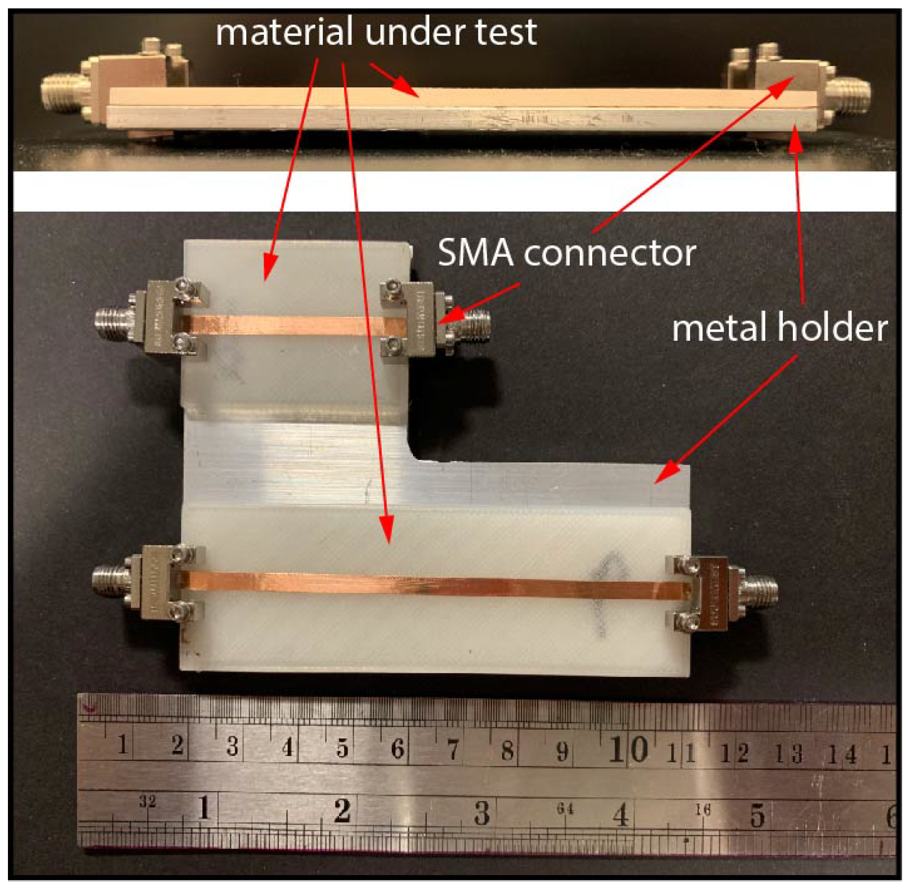
To obtain the permittivity for each of the prepared nylon substrate samples, a customized metal substrate holder and a vector network analyzer (VNA) were used to measure phase delays in the two different length substrates for each setting. The pair of AM nylon substrates had four SubMiniature version A (SMA) end-launch connectors affixed to the top surface of the CNC-milled metal substrate holder (Figure 2). Phase delay on both substrates were then measured to analyze permittivity.

2.2. Permittivity Measurement of AM Material

Conventionally, resonant methods [28,29,30] are used to determine the permittivity of bulk materials with low loss characteristics. These methods are accurate but have limited measurement frequency range or require a high volume of material for the test, which is not suitable for exploring AM parts’ permittivity. To more easily measure the permittivity of AM substrates in the lab, the two-microstrip-line method [
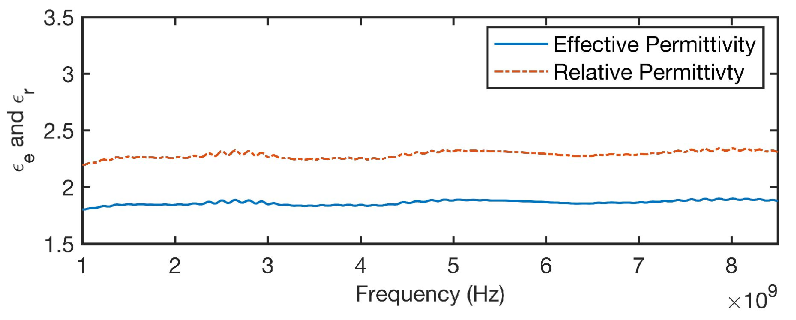
27], which is reported to have an accuracy on the order of 0.5–1.0%, was modified. Moreover, due to the process of AM, substrates built by the extrusion method usually are not perfectly flat because of warping, and the permittivity changes because of deformation. The deformation happens when testing the 3D-printed thin substrates without attaching a rigid flat back plate. The method can be flexibly used to measure the permittivity of an AM substrate of any size over a wide frequency range and can be very useful in an industrial environment where one needs to measure the deviation of the permittivity from sample to sample. The method requires two microstrip lines on two substrates of different lengths to perform the measurement. Phase delays from the responses from the two microstrip lines can then be measured by a commercial full-featured VNA (e.g., E5071C, two-port 20-GHz, Agilent Technologies). The VNA was calibrated with a 85033D 3.5-mm calibration kit. The frequency sweep range was from 1 GHz to 8.5 GHz to cover the entire frequency range of interest. The output power was set to 0 dBm, and the IF bandwidth was 1 kHz for the phase delay measurement. The phase delay data were directly exported from the VNA. With the measured phase delays and the known physical length difference of the microstrip lines on the two substrates, the permittivity can be calculated.
To determine the permittivity, first the effective permittivity that takes into account the fringing effect is obtained. Because of the fringing effect, the electric field exists not only directly between the two conductive elements of the transmission line (i.e., conductive trace and ground plane), but also extends farther from the edge of the trace. Therefore, to acquire this effective permittivity, parameters such as transmission line width and substrate thickness are taken into consideration.
The microstrip lines are essentially copper tapes of width 1/8-inch (3.18 mm) and thickness of 1 mil (one thousandth of an inch, 0.0254 mm), taped to the two different length test substrates shown in Figure 2. The difference between the lengths of the substrates is appropriately chosen to simplify calculations. Assuming the four connectors to be identical, the measured phase delay difference Δ ϕ between the two lines (or the two substrates) can be expressed as
Δ ϕ = 2 π f c ε e · ( l p 1 l p 2 ) ,
where c is the speed of light in free space, ε e is the effective permittivity of the dielectric substrate, and l p 1 and l p 2 are the physical lengths of the microstrip lines on the substrates. From Equation (1), we determined ε e of the dielectric substrate, which we then used to derive its relative permittivity ( ε r ) in the test frequency range using an analysis of the propagation constant [31]. Microstrip transmission line structure (Figure 3) usually has a conductive strip of width w and a dielectric layer of thickness H between the two conductors.
With the obtained effective permittivity, the relative permittivity ( ε e ) can be determined from the following equation.
ε e = ε r + 1 2 + ε r 1 2 1 + 12 H w 1 2 + 1 25 1 w H 2 for w H < 1 ε r + 1 2 + ε r 1 2 1 + 12 H w 1 2 for w H 1 .

3. Results and Discussion

Figure 4 shows the direct measurement result from the VNA of phase delay of two 80% infill nylon substrates with rectangular infill pattern over a frequency range of 1 GHz to 8.5 GHz. The calculated effective permittivity ε e and relative permittivity ε r are shown in Figure 5. Statistical analysis was performed on the dataset to observe significant differences between the different infill patterns in the frequency range from 2 GHz to 3 GHz .

3.1. Research Question 1

It was hypothesized that higher infill density would yield higher permittivity than lower infill density substrates, owing to the higher value of permittivity of nylon than air. The results (Figure 6) from the experiments align with this hypothesis as the permittivity shows a linear relationship ( R 2 = 0.996 ) with the infill density (over the range of 10–90% for rectangular infill pattern). A t-test shows that the permittivity for different infill densities are significantly different ( p < 0.05 , the mean difference in pairs ranging from 0.08 to 0.13). The presence of air gaps results in lower overall permittivity of the substrates. Adjusting permittivity from 10% to 90% dense structure will reduce the element size by 18% when applied to antenna design. As can be seen in Figure 7, the mesh structure of the AM nylon structure becomes denser with increasing infill density. This linear relationship between the infill density and the permittivity value gives an understanding of the relationship between manufacturing parameters and electromagnetic behavior, which are necessary in the design of microwave components. For instance, a high permittivity is needed when a microwave component needs to fit a small structure.

3.2. Research Question 2

Relative permittivity box figures of hexagonal and triangular infill patterns are shown in Figure 8 and Figure 9. It was hypothesized that different infill patterns would result in different overall permittivity of the substrates as a result of differences in mechanical properties [24]. The experimental results of rectangular, hexagonal, and triangular infill patterns with infill densities of 30%, 40%, and 50% were compared (see Figure 10). As was expected, the three infill patterns have a statistically significant difference in permittivity values for the same infill density ( p < 0.05 ). The mean difference between the pairs reduces as the density increases (from an average of 0.17 for 30% infill to 0.06 for 50% infill density). The result means that, at higher infill densities, the permittivity values tend to converge. The variation in permittivity is linear with the density as was found from Research Question 1; however, different infill patterns have significantly different slopes. Due to the nature of the FDM technique, the nozzle travels more than one time at the joint point of the infill pattern. In Figure 11, the joint areas are circled. In a rectangular pattern substrate, the nozzle travels two times at the joint point. In a hexagonal pattern substrate, the nozzle travels one time at the joint point. In a triangular pattern substrate, the nozzle travels three times at the joint point. More material is extruded at the joint area. As the infill density increases, the number of joint points in the triangular pattern substrate will grow significantly. This is the anisotropic nature of the 3D-printed substrate with FDM technique. The permittivity varies differently as the infill density is varied for different infill pattern, which is an important piece of information when designing AM microwave components for the desired frequency range. In the frequency range of 2 to 3 GHz , mean values of the relative permittivity of different infill density substrates data are shown in Table 4.

3.3. Research Question 3

It was hypothesized that increasing the roof and floor layer would result in a higher permittivity of the AM substrate due to a denser surface. The experimental results of solid pattern with 2–8 roof and floor layers were compared (Figure 12). Experiments on substrates printed with solid infill type with different numbers of the roof and floor layers also show a statistically significant difference in relative permittivity ( p < 0.05 ). However, the mean differences in the groups were low (ranging from 0.014 to 0.079). In the frequency range of 2 to 3 GHz , mean values of the relative permittivity of solid infill pattern and a PA66 nylon sheet are shown in Table 5.

4. Case Study: AM Patch Antenna Design

Based on the permittivity measurement method described and relative permittivity value obtained, an AM patch antenna was designed and implemented on an AM nylon substrate. As previously discussed, fabricating antennas with AM offers the advantages of low cost, faster production, and flexibility in design [32,33,34]. Once a particular patch shape for an application is selected, the resonant frequency, polarization, pattern, and impedance can be adjusted based on the size and material of the patch antenna. Then, after accurately obtaining the permittivity of the AM nylon substrate, the dimensions of the AM patch antenna can be calculated for a required frequency [16]. The AM patch antenna demonstrated in this section was designed for the 2.5-GHz WiMAX band.
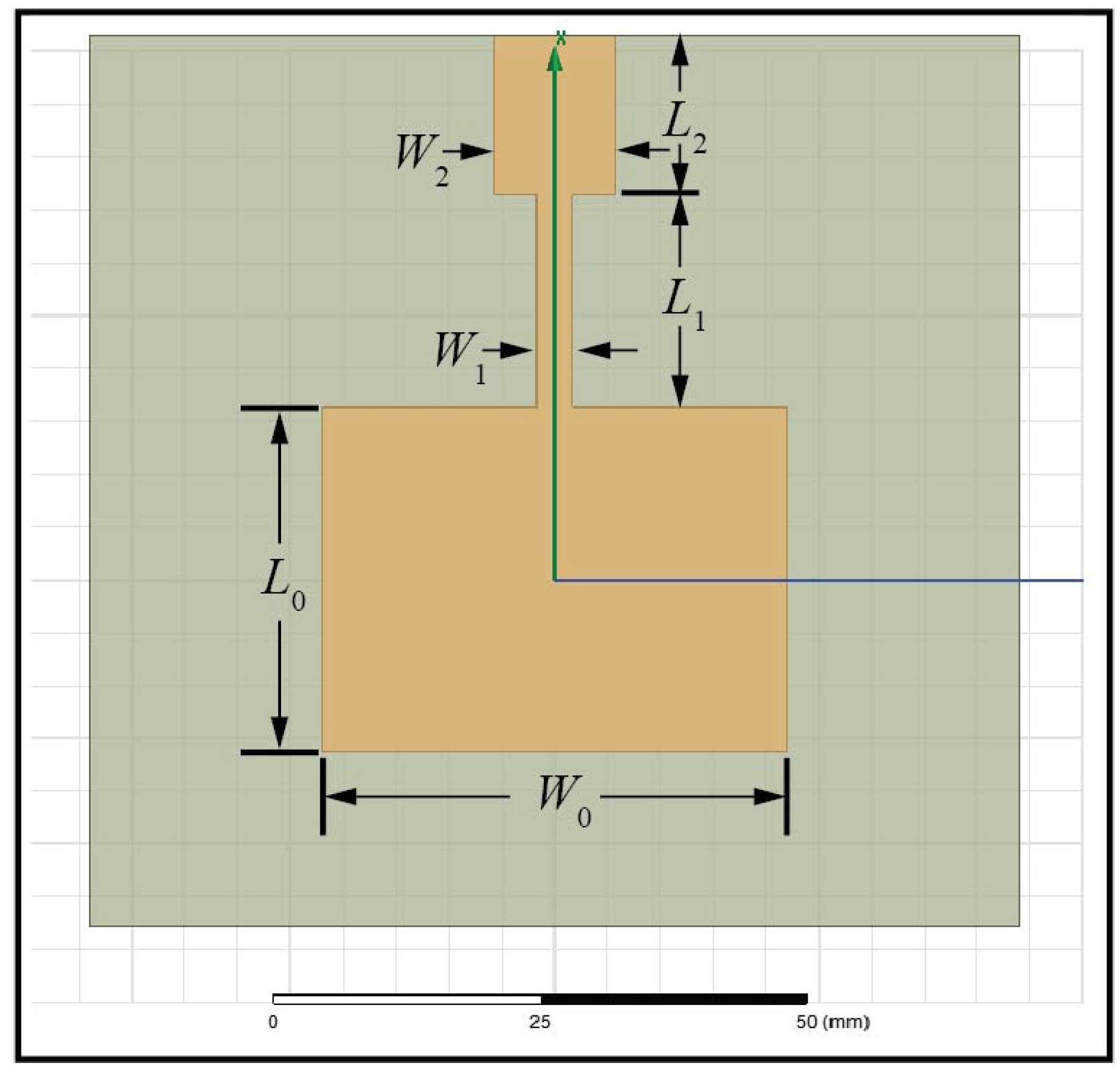
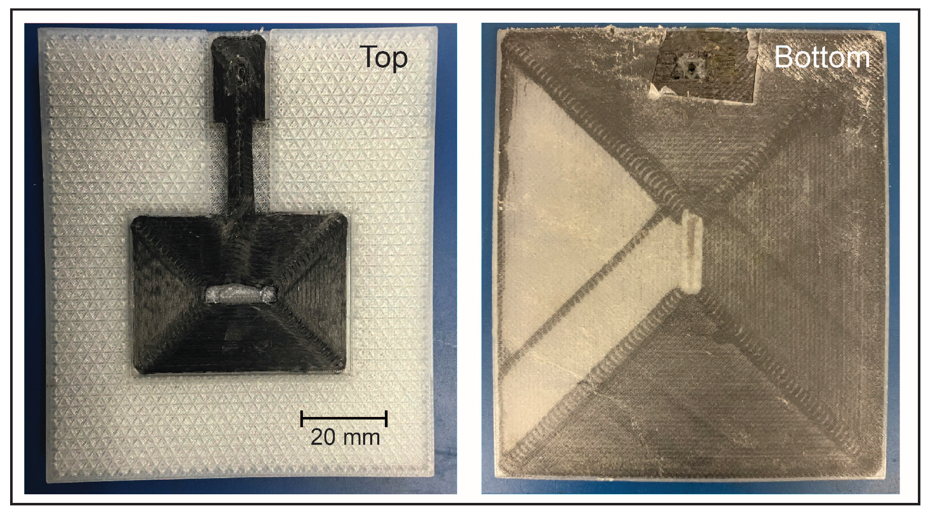
The patch antenna (shown in Figure 13) was designed to be fed by a quarter-wavelength microstrip transmission line to match the impedance of the antenna source [35]. The patch antenna, microstrip transmission line, and ground plane were made of nylon re-enforced with conductive, continuous, carbon fiber filament. The nylon substrate also integrated a ground plane with the conductive carbon-fiber material on the back of the structure (see Figure 14). The ground plane was a part of the patch antenna structure. Due to the resolution of the printer, the thickness of the substrate had to be no less than 5 m m so that a 3-layer carbon-fiber ground plane could be integrated into the substrate. Since the Eiger slicing software does not allow the user to selectively place the continuous carbon fiber, the patch antenna was separately printed and embedded into a designed cavity on the substrate (see Figure 14). The thickness of the carbon-fiber patch antenna was designed to be 0.5 m m from the top of the ground plane to the bottom of the patch antenna. These dimensions for the patch antenna were calculated from antenna design equations [16,36,37], and a piece of AM nylon substrate of triangular infill pattern with 60% infill density was used. Dimensions were further optimized with ANSYS Electronics Desktop to maximize the bandwidth and adjust the resonant frequency at 2.5 G Hz by linearly sweeping the key parameters in Table 6.
The AM patch antenna made of nylon and carbon fiber is shown in 
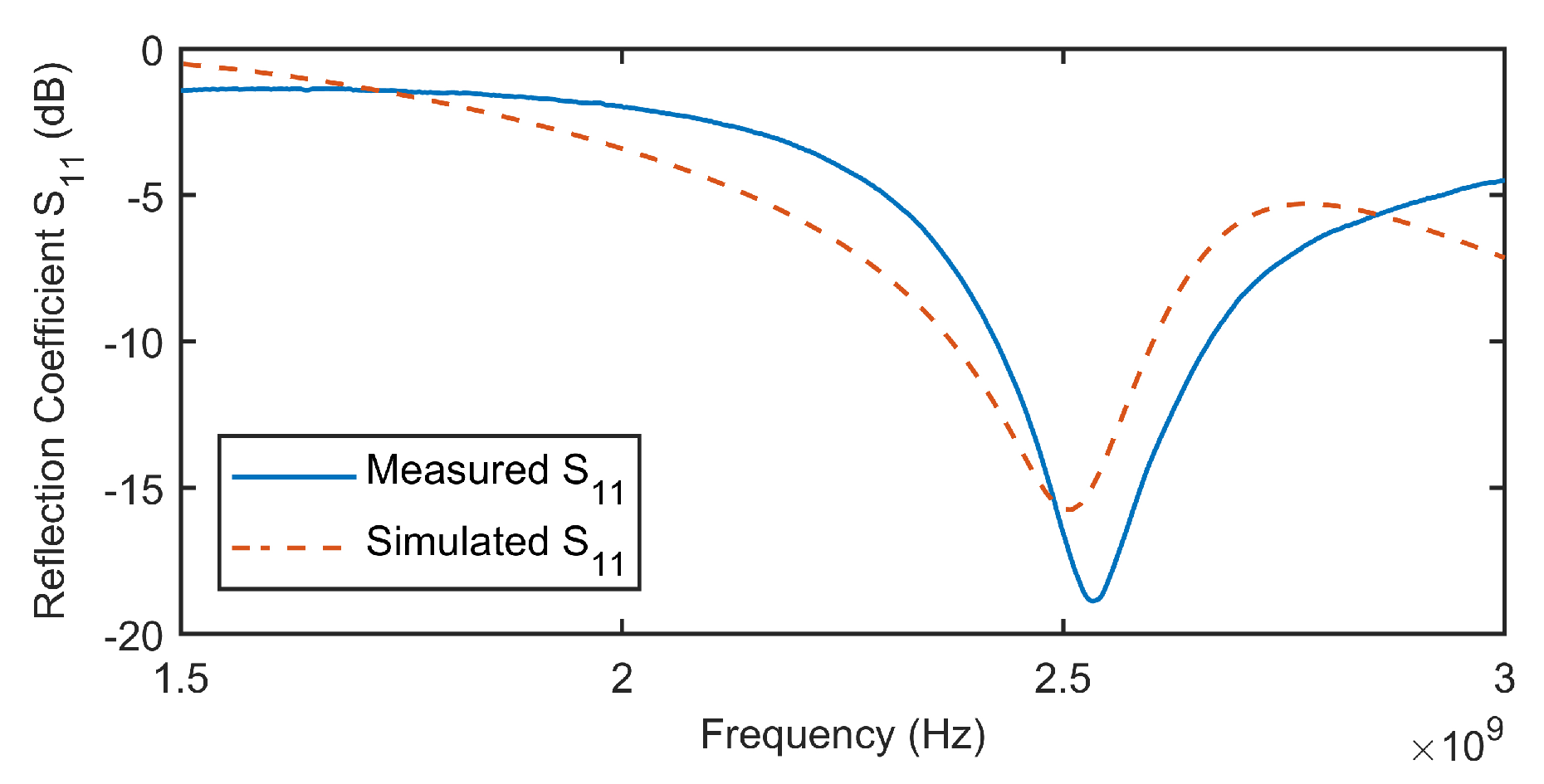
Figure 14. The magnitude of the reflection coefficient S 11 of the AM patch antenna was measured using a VNA, and the result is shown in Figure 15, together with the numerical simulation result obtained via ANSYS Electronics Desktop. With specified infill density and infill pattern, we determined the permittivity of the AM substrate for the patch antenna design based on the data from previous permittivity measurements. The measured resonant frequency of the patch antenna shifted up by 30 M Hz with respect to the simulation result, corresponding to a frequency shift of 1.2%.

5. Conclusions

In this article, we have developed a procedure for measuring the permittivity of AM nylon substrates with low volume material cost and investigated relations between the variation of permittivity and different print parameters such as infill density, infill pattern, and the number of roof and floor layers. As was hypothesized, the measured relative permittivity of the AM nylon substrates with rectangular infill pattern displayed a linear relationship with infill density range from 10% to 90%. The permittivity of the AM substrates also changed with different infill patterns, indicating the effect of material deposition paths. Adding roof and floor layers slightly increased the permittivity of the AM substrates with a solid infill pattern. This understanding gives us control over the relative permittivity of the AM substrate by adjusting the infill density, infill pattern, and the number of roof and floor layers to facilitate better control of the microwave component design. The permittivity measurement method used can also be extended to other AM processes and help facilitate the design of AM microwave components with nanoparticle conductive ink, and unique designs of antennas. The obtained relative permittivity was applied to the design of an AM patch antenna, including an AM nylon substrate and a carbon-fiber patch for the desired frequency. The measured reflection coefficient results show good agreement with simulation results, demonstrating that the obtained permittivity values can be directly used for the AM patch antenna designs. The permittivity was found to vary linearly with the infill densities for different infill patterns, allowing interpolation for prediction of permittivity for any infill density. After knowing the relationships between permittivity and AM build parameters, the permittivity value can be programmed to realize varying local permittivity in an AM structure. The gradually changed permittivity structure can also be used to reduce reflection and improve the efficiency of the microwave component when embedding into an AM part. This provides flexibility in the design of AM microwave components, enabling its customization.

Author Contributions

Conceptualization, methodology, experimentation, data curation, writing—original draft preparation, H.H.; research guidance, S.G.B.; specimen design and preparation, S.S.; experimental design, N.M.; writing—review and editing, S.S., N.M., and S.G.B. All authors have read and agreed to the published version of the manuscript.

Funding

This research received no external funding.

Acknowledgments

The authors would like to thank Yimin Ding for his support with microscope images.

Conflicts of Interest

The authors declare no conflict of interest.

References

  1. Atzeni, E.; Salmi, A. Economics of additive manufacturing for end-usable metal parts. Int. J. Adv. Manuf. Technol. 2012, 62, 1147–1155. [Google Scholar] [CrossRef]
  2. Klahn, C.; Leutenecker, B.; Meboldt, M. Design strategies for the process of additive manufacturing. Procedia CIRP 2015, 36, 230–235. [Google Scholar] [CrossRef] [Green Version]
  3. Macdonald, E.; Salas, R.; Espalin, D.; Perez, M.; Aguilera, E.; Muse, D.; Wicker, R.B. 3D printing for the rapid prototyping of structural electronics. IEEE Access 2014, 2, 234–242. [Google Scholar] [CrossRef]
  4. Yu, Y.Z.; Lu, J.R.; Liu, J. 3D printing for functional electronics by injection and package of liquid metals into channels of mechanical structures. Mater. Des. 2017, 122, 80–89. [Google Scholar] [CrossRef]
  5. Conner, B.P.; Manogharan, G.P.; Martof, A.N.; Rodomsky, L.M.; Rodomsky, C.M.; Jordan, D.C.; Limperos, J.W. Making sense of 3-D printing: Creating a map of additive manufacturing products and services. Addit. Manuf. 2014, 1, 64–76. [Google Scholar] [CrossRef]
  6. Manessis, D.; Podlasly, A.; Ostmann, A.; Aschenbrenner, R.; Lang, K.D. Large-scale manufacturing of embedded subsystems-in-substrates and a 3D-stacking approach for a miniaturised medical system integration. In Proceedings of the 2013 Eurpoean Microelectronics Packaging Conference (EMPC), Grenoble, France, 9–12 September 2013; pp. 1–6. [Google Scholar]
  7. O’Brien, J.M.; Rojas, E.; Weller, T.M. A switched-line phase shifter fabricated with additive manufacturing. In Proceedings of the International Symposium on Microelectronics 2013, Orlando, FL, USA, 30 September–3 October 2013; International Microelectronics Assembly and Packaging Society: Research Triangle Park, NC, USA, 2013; Volume 2013, pp. 909–913. [Google Scholar]
  8. Robles Dominguez, U. 3D Printed Impedance Elements by Micro-Dispensing. Ph.D. Thesis, Electrical Engineering, University of Texas at El Paso, El Paso, TX, USA, 2013. [Google Scholar]
  9. Adams, J.J.; Duoss, E.B.; Malkowski, T.F.; Motala, M.J.; Ahn, B.Y.; Nuzzo, R.G.; Bernhard, J.T.; Lewis, J.A. Conformal printing of electrically small antennas on three-dimensional surfaces. Adv. Mater. 2011, 23, 1335–1340. [Google Scholar] [CrossRef] [PubMed]
  10. Salonen, P.; Kupiainen, V.; Tuohimaa, M. Direct printing of a handset antenna on a 3D surface. In Proceedings of the 2013 IEEE Antennas and Propagation Society International Symposium (APSURSI), Orlando, FL, USA, 7–13 July 2013; pp. 504–505. [Google Scholar]
  11. Koskinen, S.; Pykäri, L.; Mäntysalo, M. Electrical performance characterization of an inkjet-printed flexible circuit in a mobile application. IEEE Trans. Compon. Packag. Manuf. Technol. 2013, 3, 1604–1610. [Google Scholar] [CrossRef]
  12. Arnal, N.; Ketterl, T.; Vega, Y.; Stratton, J.; Perkowski, C.; Deffenbaugh, P.; Church, K.; Weller, T. 3D multi-layer additive manufacturing of a 2.45 GHz RF front end. In Proceedings of the 2015 IEEE MTT-S International Microwave Symposium, Phoenix, AZ, USA, 17–22 May 2015; pp. 1–4. [Google Scholar]
  13. Lopes, A.J.; MacDonald, E.; Wicker, R.B. Integrating stereolithography and direct print technologies for 3D structural electronics fabrication. Rapid Prototyp. J. 2012, 18, 129–143. [Google Scholar] [CrossRef]
  14. Shemelya, C.; Zemba, M.; Liang, M.; Espalin, D.; Kief, C.; Xin, H.; Wicker, R.; MacDonald, E. 3D printing multi-functionality: Embedded RF antennas and components. In Proceedings of the 2015 9th European Conference on Antennas and Propagation (EuCAP), Lisbon, Portugal, 12–17 April 2015; pp. 1–5. [Google Scholar]
  15. Liu, B.; Gong, X.; Chappell, W.J. Applications of layer-by-layer polymer stereolithography for three-dimensional high-frequency components. IEEE Trans. Microw. Theory Tech. 2004, 52, 2567–2575. [Google Scholar] [CrossRef]
  16. Espalin, D.; Muse, D.W.; MacDonald, E.; Wicker, R.B. 3D Printing multifunctionality: Structures with electronics. Int. J. Adv. Manuf. Technol. 2014, 72, 963–978. [Google Scholar] [CrossRef]
  17. Balanis, C.A. Antenna Theory: Analysis and Design; John Wiley & Sons: Hoboken, NJ, USA, 2016. [Google Scholar]
  18. Moscato, S.; Bahr, R.; Le, T.; Pasian, M.; Bozzi, M.; Perregrini, L.; Tentzeris, M.M. Infill-dependent 3-D-printed material based on NinjaFlex filament for antenna applications. IEEE Antennas Wirel. Propag. Lett. 2016, 15, 1506–1509. [Google Scholar] [CrossRef]
  19. Bahr, R.; Le, T.; Tentzeris, M.M.; Moscato, S.; Pasian, M.; Bozzi, M.; Perregrini, L. RF characterization of 3D printed flexible materials-NinjaFlex filaments. In Proceedings of the 2015 European Microwave Conference (EuMC), Orlando, FL, USA, 7–13 July 2015; pp. 742–745. [Google Scholar]
  20. Tomassoni, C.; Bahr, R.; Tentzeris, M.; Bozzi, M.; Perregrini, L. 3D printed substrate integrated waveguide filters with locally controlled dielectric permittivity. In Proceedings of the 2016 46th European Microwave Conference (EuMC), London, UK, 3–7 October 2016; pp. 253–256. [Google Scholar]
  21. Renou, R.; Ding, M.; Zhu, H.; Szymczyk, A.; Malfreyt, P.; Ghoufi, A. Concentration dependence of the dielectric permittivity, structure, and dynamics of aqueous NaCl solutions: Comparison between the Drude oscillator and electronic continuum models. J. Phys. Chem. B 2014, 118, 3931–3940. [Google Scholar] [CrossRef] [PubMed]
  22. Goulas, A.; Zhang, S.; Cadman, D.A.; Järveläinen, J.; Mylläri, V.; Whittow, W.G.; Vardaxoglou, J.Y.C.; Engstrøm, D.S. The impact of 3D printing process parameters on the dielectric properties of high permittivity composites. Designs 2019, 3, 50. [Google Scholar] [CrossRef] [Green Version]
  23. 3D Matter. What is the Influence of Infill My 3D Prints? Available online: https://my3dmatter.com/influence-infill-layer-height-pattern/ (accessed on 10 August 2020).
  24. Lubombo, C.; Huneault, M.A. Effect of infill patterns on the mechanical performance of lightweight 3D-printed cellular PLA parts. Mater. Today Commun. 2018, 17, 214–228. [Google Scholar] [CrossRef]
  25. Omari, M.A.; Sevostianov, I. Estimation of changes in the mechanical properties of stainless steel subjected to fatigue loading via electrical resistance monitoring. Int. J. Eng. Sci. 2013, 65, 40–48. [Google Scholar] [CrossRef]
  26. Markforged. Eiger Glossary. Available online: https://support.markforged.com/portal/s/article/Eiger-Glossary (accessed on 10 August 2020).
  27. Das, N.K.; Voda, S.M.; Pozar, D.M. Two methods for the measurement of substrate dielectric constant. IEEE Trans. Microw. Theory Tech. 1987, 35, 636–642. [Google Scholar] [CrossRef]
  28. Howell, J.Q. A quick accurate method to measure the dielectric constant of microwave integrated-circuit substrates (short papers). IEEE Trans. Microw. Theory Tech. 1973, 21, 142–144. [Google Scholar] [CrossRef]
  29. Napoli, L.; Hughes, J. A simple technique for the accurate determination of the microwave dielectric constant for microwave integrated circuit substrates (Correspondence). IEEE Trans. Microw. Theory Tech. 1971, 19, 664–665. [Google Scholar] [CrossRef]
  30. Ladbrooke, P.; Potok, M.; England, E. Coupling Errors in Cavity-Resonance Measurements on MIC Dielectrics (Short Papers). IEEE Trans. Microw. Theory Tech. 1973, 21, 560–562. [Google Scholar] [CrossRef]
  31. Das, N.K.; Pozar, D.M. A generalized spectral-domain Green’s function for multilayer dielectric substrates with application to multilayer transmission lines. IEEE Trans. Microw. Theory Tech. 1987, 35, 326–335. [Google Scholar] [CrossRef]
  32. Breed, G. The fundamentals of patch antenna design and performance. High Freq. Electron. 2009, 3, 49–51. [Google Scholar]
  33. Herd, J.; Carlson, D.; Duffy, S.; Weber, M.; Brigham, G.; Rachlin, M.; Cursio, D.; Liss, C.; Weigand, C. Multifunction Phased Array Radar (MPAR) for aircraft and weather surveillance. In Proceedings of the 2010 IEEE Radar Conference, Washington, DC, USA, 10–14 May 2010; pp. 945–948. [Google Scholar]
  34. Jones, H.S., Jr. Multifrequency Antenna System Integrated into a Radome. U.S. Patent 4,101,895, 18 July 1978. [Google Scholar]
  35. Hu, H. Development of a Radio-Frequency Front-End for an Ice-Penetrating Radar. Master’s Thesis, Electrical Engineering, The Pennsylvania State University, University Park, PA, USA, 2015. [Google Scholar]
  36. Hammerstad, E.O. Equations for microstrip circuit design. In Proceedings of the 1975 5th European Microwave Conference, Hamburg, Germany, 4–6 October 1975; pp. 268–272. [Google Scholar]
  37. Balanis, C.A. Advanced Engineering Electromagnetics; John Wiley & Sons: Hoboken, NJ, USA, 2012; pp. 459–464. [Google Scholar]
Figure 1. Extrusion AM substrates: (a) Rectangular infill pattern. (b) Hexagonal infill pattern. (c) Triangular infill pattern.
Designs 04 00039 g001
Figure 2. AM nylon substrates with SMA connectors on the test platform.
Designs 04 00039 g002
Figure 3. Microstrip transmission line structure cross-section.
Designs 04 00039 g003
Figure 4. Phase delays of rectangular infill pattern (80% infill density) vs. frequency.
Designs 04 00039 g004
Figure 5. Effective permittivity and relative permittivity of rectangular infill pattern (80% infill density) vs. frequency.
Designs 04 00039 g005
Figure 6. Relative permittivity box figures of rectangular infill pattern.
Designs 04 00039 g006
Figure 7. Microscope images of rectangular infill pattern (10%, 50% and 90% infill density).
Designs 04 00039 g007
Figure 8. Relative permittivity box figures of hexagonal infill pattern.
Designs 04 00039 g008
Figure 9. Relative permittivity box figures of triangular infill pattern.
Designs 04 00039 g009
Figure 10. Comparison of relative permittivity between different infill patterns.
Designs 04 00039 g010
Figure 11. Microscope images of rectangular, hexagonal, and triangular infill pattern of 30% infill density.
Designs 04 00039 g011
Figure 12. Relative permittivity box figures of solid infill pattern (2–8 roof and floor layers).
Designs 04 00039 g012
Figure 13. Patch antenna layout on ANSYS Electronics Desktop.
Designs 04 00039 g013
Figure 14. Fabricated AM patch antenna with nylon substrate and carbon fiber patch.
Designs 04 00039 g014
Figure 15. AM patch antenna reflection coefficient S 11 simulation and test results.
Designs 04 00039 g015
Table 1. Nylon substrates information from Eiger for Research Question 1.
Infill PatternInfill DensityRoof & Floor LayersPart Mass (g)Material Vol. (cm 3 )Print Time (min.)
Rectangular10%44.814.3752
20%45.284.8056
30%45.755.2360
40%46.195.6264
50%46.656.0567
60%47.126.4771
70%47.596.9075
80%48.057.3279
90%48.527.7583
Table 2. Nylon substrates information from Eiger for Research Question 2.
Infill PatternInfill DensityRoof & Floor LayersPart Mass (g)Material Vol. (cm 3 )Print Time (min.)
Hexagonal30%45.725.2067
40%46.155.5975
50%46.636.0384
Triangular30%45.725.2060
40%46.195.6264
50%46.716.1068
Table 3. Nylon substrates information from Eiger for Research Question 3.
Infill PatternInfill DensityRoof & Floor LayersPart Mass (g)Material Vol. (cm 3 )Print Time (min.)
Solid100%28.747.9484
100%48.808.0085
100%68.868.0686
100%88.938.1186
Table 4. Relative permittivity of different substrates.
Infill DensityMean Value of ε r @ 2 GHz–3 GHz
RectangularHexagonalTriangular
10%1.6095--
20%1.6903--
30%1.77221.89631.6478
40%1.88571.97621.8172
50%1.96872.06462.0188
60%2.0846--
70%2.2203--
80%2.2872--
90%2.3963--
Table 5. Relative permittivity of solid substrates.
Infill PatternRoof & Floor LayersMean Value of ε r @ 2 GHz–3 GHz
Solid2 layers2.6571
4 layers2.6714
6 layers2.7185
8 layers2.7981
PA66 Nylon SheetSolid3.0745
Table 6. Calculated and optimized dimensions by ANSYS electronic desktop.
ParameterCalculated Value (mm)Optimized Value (mm)Dev. (%)
H (substrate thickness)5.05.00.0
h (patch height)0.50.50.0
L 0 35.332.7 7.4
W 0 45.844.0 4.1
L 1 20.120.10
W 1 3.83.5 7.9
L 2 15.015.00
W 2 10.811.4 5.6

