Comprehensive Understanding of Hillocks and Ion Tracks in Ceramics Irradiated with Swift Heavy Ions


1
Nuclear Science and Engineering Center, Japan Atomic Energy Agency (JAEA), Tokai, Ibaraki 319-1195, Japan
2
Quantum Beam Science Research Directorate, National Institutes for Quantum and Radiological Science and Technology (QST), Tokai, Ibaraki 319-1106, Japan
*
Author to whom correspondence should be addressed.
Quantum Beam Sci. 2020, 4(4), 43; https://0-doi-org.brum.beds.ac.uk/10.3390/qubs4040043
Submission received: 13 November 2020
/
Revised: 8 December 2020
/
Accepted: 8 December 2020
/
Published: 9 December 2020
(This article belongs to the Special Issue The Modifications of Metallic and Inorganic Materials by Using Energetic Ion/Electron Beams)
Abstract
:Amorphizable ceramics (LiNbO3, ZrSiO4, and Gd3Ga5O12) were irradiated with 200 MeV Au ions at an oblique incidence angle, and the as-irradiated samples were observed by transmission electron microscopy (TEM). Ion tracks in amorphizable ceramics are confirmed to be homogenous along the ion paths. Magnified TEM images show the formation of bell-shaped hillocks. The ion track diameter and hillock diameter are similar for all the amorphizable ceramics, while there is a tendency for the hillocks to be slightly bigger than the ion tracks. For SrTiO3 (STO) and 0.5 wt% niobium-doped STO (Nb-STO), whose hillock formation has not been fully explored, 200 MeV Au ion irradiation and TEM observation were also performed. The ion track diameters in these materials are found to be markedly smaller than the hillock diameters. The ion tracks in these materials exhibit inhomogeneity, which is similar to that reported for non-amorphizable ceramics. On the other hand, the hillocks appear to be amorphous, and the amorphous feature is in contrast to the crystalline feature of hillocks observed in non-amorphizable ceramics. No marked difference is recognized between the nanostructures in STO and those in Nb-STO. The material dependence of the nanostructure formation is explained in terms of the intricate recrystallization process.
1. Introduction
Long nanometer-sized damage trails are created in ceramics continuously along the trajectories of swift heavy ions (SHIs), if the energy transfer from a SHI to an electron system of ceramics is sufficiently high [1,2,3]. Such characteristic damage is called an ion track. The mechanism of ion track formation has been extensively studied so far, and it has been one of the central topics in the research on ion-solid interactions. Ceramics can be categorized into two groups; amorphizable and non-amorphizable ceramics. If amorphous ion tracks are created, the ceramics are called amorphizable ceramics. The electronic stopping power dependence of ion track sizes in many amorphizable ceramics has been successfully predicted using the thermal spike model [4,5,6,7,8]. According to the model, the amorphous ion track formation is attributable to a local temperature rise sufficient to cause local melting along an ion path. On the other hand, there are non-amorphizable ceramics in which a crystal structure within an ion track region is not amorphized [9,10,11,12,13,14]. It has been found that in non-amorphizable ceramics, ion track size is markedly smaller than the size of the melt predicted by the thermal spike models [13,14]. Recent molecular dynamics (MD) simulation has revealed that the small ion tracks in non-amorphizable ceramics are attributable to fast recrystallization after transient melting [15,16,17,18]. It has been pointed out that the ionic nature of atomic bonding in non-amorphizable ceramics may be responsible for such fast recrystallization in non-amorphizable ceramics [9,19]. However, there is currently no consensus on which material property makes the distinction between amorphizable and non-amorphizable ceramics. Therefore, it is important to examine the material dependence of ion track formation in terms of amorphization/recrystallization.
Ion track formation caused by SHIs is often accompanied by the formation of hillocks (so-called surface ion tracks) [20,21,22,23,24,25,26,27,28,29,30,31,32,33,34,35]. Our recent studies revealed that both ion tracks and hillocks are amorphous in the case of amorphizable ceramics (Y3Fe5O12 (YIG)) [36,37], whereas crystalline hillocks are found in the case of non-amorphizable ceramics (CaF2, SrF2, BaF2, and CeO2) [36,38]. Since the surface protrusion is a direct consequence of local melting along the ion path (melting of the ion track region), the observation of crystalline hillocks in non-amorphizable ceramics also provides a strong evidence of recrystallization after melting of the ion track region. It was also found that the hillock diameter always coincides with the diameter of a melt predicted by the thermal spike model for both amorphizable and non-amorphizable ceramics. This means that a hillock diameter value is affected by a melting process, but it remains unchanged after the subsequent recrystallization process. It is likely that a hillock size reflects melting, whereas an ion track size reflects both melting and subsequent recrystallization. Therefore, a comparative analysis of ion tracks and hillocks allows us to elucidate the whole processes of melting and amorphization/recrystallization. Moreover, there must be a variety of hillock and ion track morphologies due to an intricate recrystallization process, which can be the origin of the material dependence of nanostructure formation.
We recently proposed a method for precise measurement of a hillock size by transmission electron microscopy (TEM) [36,37,38]. The method is useful for the direct observation of a hillock side-view. It allows the accurate measurement of hillock dimensions and the identification of hillock crystal structure. In our previous study, we have studied hillocks and ion tracks in non-amorphizable ceramics such as CaF2, SrF2, and BaF2, whereas only one amorphizable ceramic (YIG) has been studied [36,37]. In the present study, we have further studied the relationship between the hillock diameter and ion track diameter for various types of ceramics. First, we show results of the TEM observations for SHI-irradiated amorphizable ceramics such as LiNbO3, ZrSiO4, and Gd3Ga5O12 (GGG) and then for SrTiO3 (STO) and 0.5 wt% niobium-doped STO (Nb-STO), whose hillock formation has not been fully explored. The electrical resistivity of STO increases by more than nine orders of magnitude by doping with 0.5 wt% Nb, whereas its crystal structure remains unaffected by the doping [39]. The effect of Nb doping on its hillock morphology is also investigated in this study. Based on the TEM investigations of both amorphizable and non-amorphizable ceramics, we discuss how the SHI-induced nanostructure formation depends on the intricate recrystallization process.
2. Experiments
Thin samples for TEM observations were prepared before irradiation by the following procedure. The original materials were ZrSiO4 (98%) powder (Kojundo Chemical Laboratory Co., Ltd., Saitama, Japan), LiNbO3 single crystals (Onizawa Fine Product Co., Ltd., Ibaraki, Japan), Gd3Ga5O12 (GGG) single crystals (Rare Metallic Co., Ltd., Tokyo, Japan), SrTiO3 (STO) single crystals (Shinkosha Co., Ltd., Kanagawa, Japan), and 0.5 wt% niobium-doped STO (Nb-STO) single crystals (Shinkosha Co., Ltd., Kanagawa, Japan). The original materials were finely ground using an agate mortar and pestle. For the preparation of LiNbO3 specimens, first, 3 mm diameter nickel grids with 2000 lines/inch were coated using 0.5% Neoprene W in toluene (Nisshin EM Co., Ltd., Tokyo, Japan), which works as an adhesive agent, and then the ground LiNbO3 powder was randomly dispersed on the grids. For the preparation of materials other than LiNbO3, the ground samples were dispersed in ethanol by an ultrasonic bath for a few minutes, and then the ethanol was dropped on 3 mm diameter 200 mesh copper grids covered with porous carbon films. The grids were then air-dried at room temperature. The samples on the grids were subsequently irradiated with 200 MeV Au32+ ions at an oblique incidence angle (45° relative to normal direction) at room temperature in a tandem accelerator at JAEA-Tokai (Japan Atomic Energy Agency, Tokai Research and Development Center, Tokai, Japan). The charge state (32+) was chosen to ensure the charge of the incident ions to have the average value of the equilibrium charge. The samples were irradiated with ions at 1 × 10¹¹ ions/cm2. The as-irradiated samples were examined using a transmission electron microscope (TEM, Model 2100F, JEOL Ltd., Tokyo, Japan) operated at 200 kV. The ion track size was measured using the TEM images taken at a low magnification, wherein clear line-like contrasts were expected to be imaged. On the other hand, the hillock size was measured using the TEM images taken at a high magnification, wherein a clear contour of hillocks was expected to be obtained. The electronic stopping power (Se) was estimated using SRIM-2008 [40,41].
3. Results and Discussions
3.1. Dimensions of Hillocks and Ion Tracks in LiNbO3, ZrSiO4, and GGG
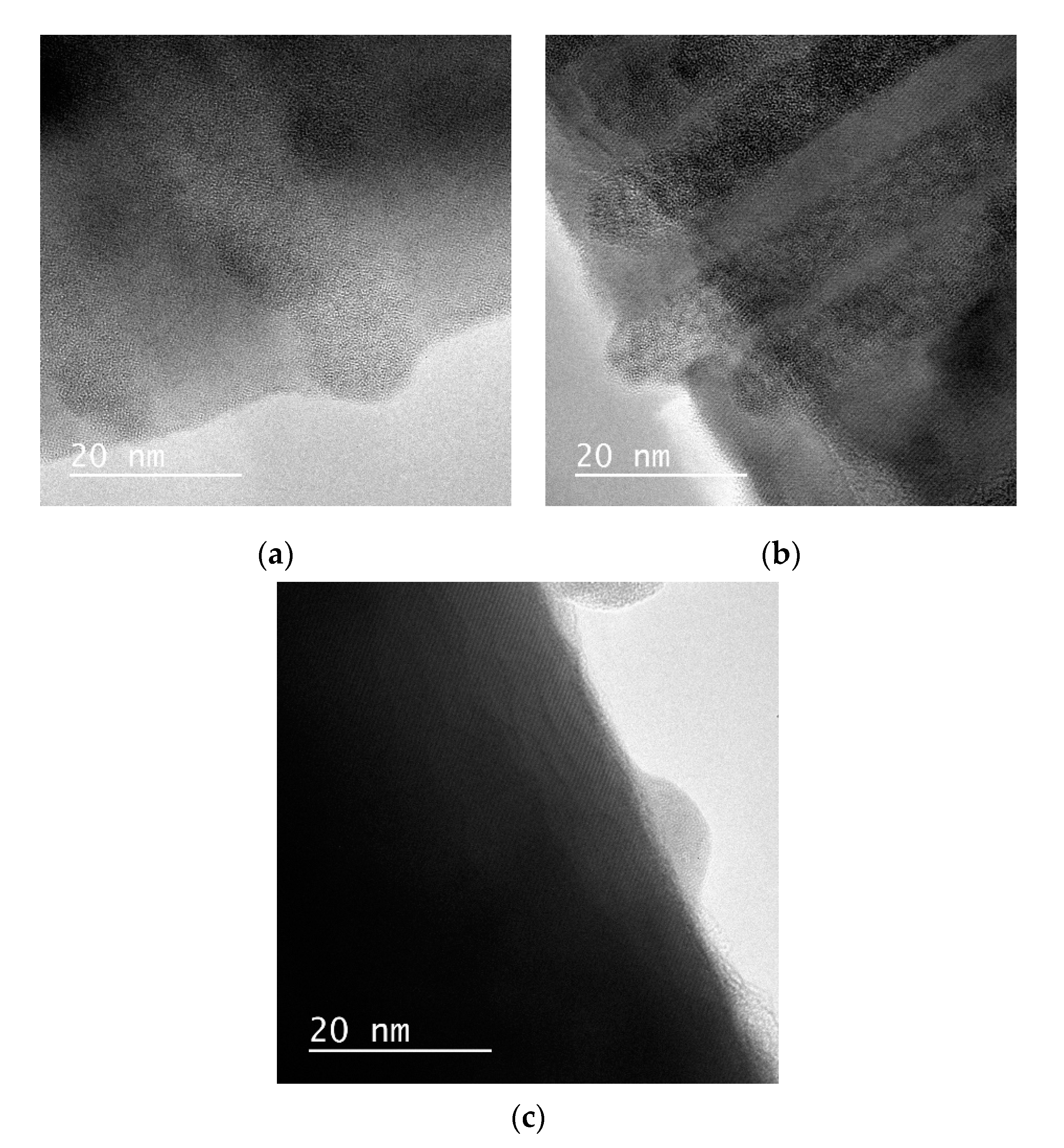
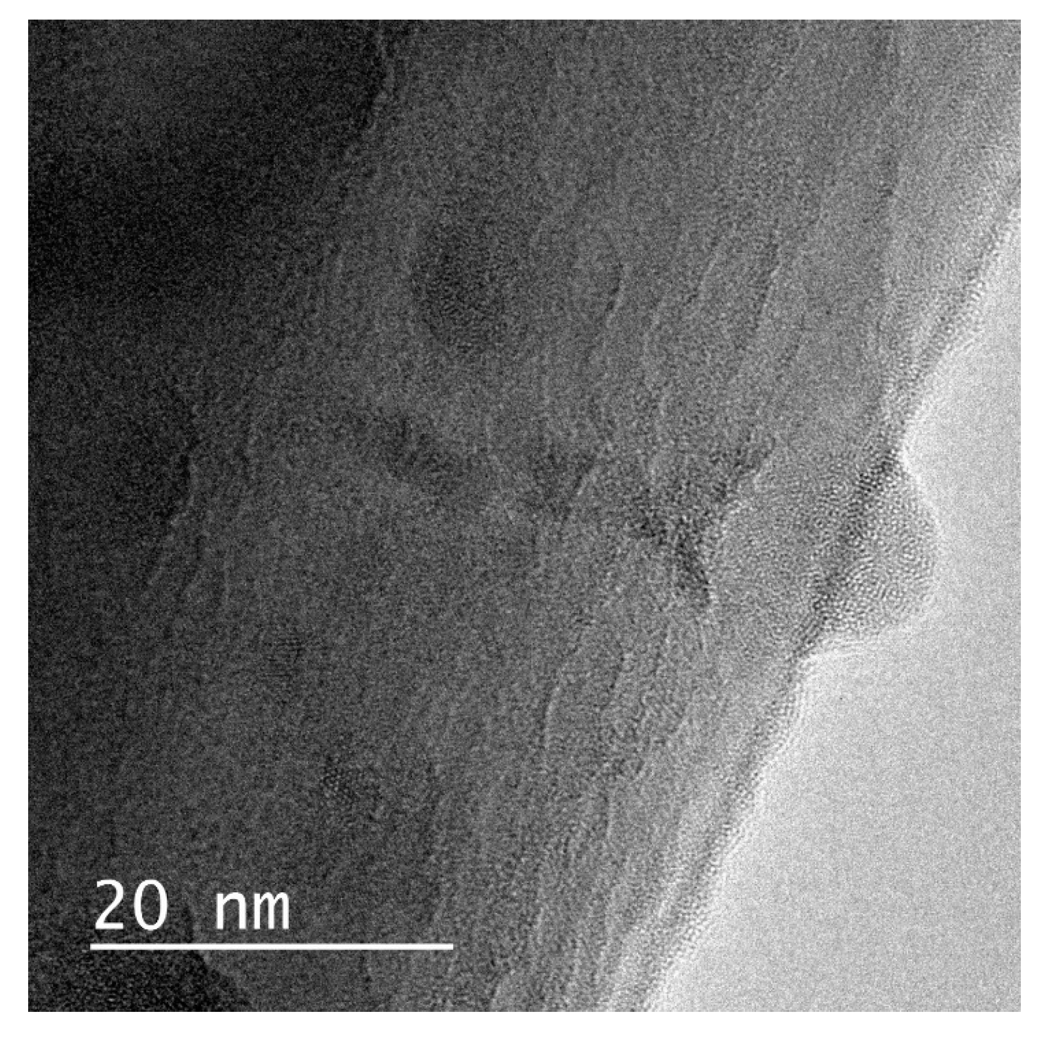
We have observed nanostructures created by SHI irradiation in amorphizable ceramics using TEM. Figure 1a–c show the bright field images of ion tracks in LiNbO3, ZrSiO4, and Gd3Ga5O12 irradiated with 200 MeV Au at an oblique incidence angle. In the figures, the ion tracks are imaged as line-like contrasts. The diameter of the ion tracks can be estimated by measuring the width of the line-like contrasts. However, for most of the ion track images, it is difficult to distinguish the ion track contrasts from hillock contrasts. However, if the hillocks are created at the edge of the samples, it is possible to infer the hillock side-view. It can be concluded from the images that hillocks have similar diameters to those of ion tracks. Size distribution of ion tracks is shown in Figure 2. The average sizes of the hillocks and ion tracks are summarized in Table 1.
Previous literatures have reported ion track sizes in LiNbO3 [42,43,44,45], ZrSiO4 [46,47], and GGG [45,48]. They have confirmed that the ion tracks in these ceramics are amorphous. A good summary of the ion track data in LiNbO3 is given in Ref. [45], in which the dependence of ion track size on the electronic stopping power (Se) is shown. The Se-dependence demonstrates that an ion track size depends primarily on the electronic stopping power, whereas low ion velocity acts as a secondary factor that contributes to a bigger ion track owing to the velocity effect [49]. The literature also demonstrates that ion track sizes are in accordance with the values predicted by the thermal spike model. The present study shows that the ion track diameter in LiNbO3 irradiated with 200 MeV Au (Se = 28.1 keV/nm) is 11.7 ± 1.3 nm, whereas the previous study showed that the ion track diameter in LiNbO3 irradiated with 201 MeV U ions (Se = 28.1 keV/nm) was around 13 nm [44,45], indicating that the present study is in accordance with the previous results within the experimental error.
Previous studies reported that the ion track diameter for ZrSiO4 irradiated with 10 GeV Pb ions (Se = 20.0 keV/nm) was 5.2 ± 0.2 nm [46] and that for ZrSiO4 irradiated with 2.9 GeV Pb ions (Se = 33.6 keV/nm) [47] was 8 nm. The present study shows that the ion track diameter for ZrSiO4 irradiated with 200 MeV Au ions is 9.5 ± 0.5 nm, exhibiting large ion tracks. Since the large ion tracks observed in the present study could be due to the relatively high electronic stopping power (Se = 29.6 keV/nm) and the velocity effect [49], there is no contradiction between the present and previous results.
A good summary of the previous ion track data in GGG is given in Ref. [45]. The present study shows that the ion track diameter for GGG irradiated with 200 MeV Au (Se = 34.0 keV/nm) is 11.3 ± 0.9 nm, whereas a previous study shows a similar ion track diameter (12.4 ± 1.6 nm for GGG irradiated with 250 MeV Pb ions (Se = 34.0 keV/nm)) [45]. Therefore, the present result is consistent with the previous results. The present results are also consistent with the prediction made by the thermal spike model.
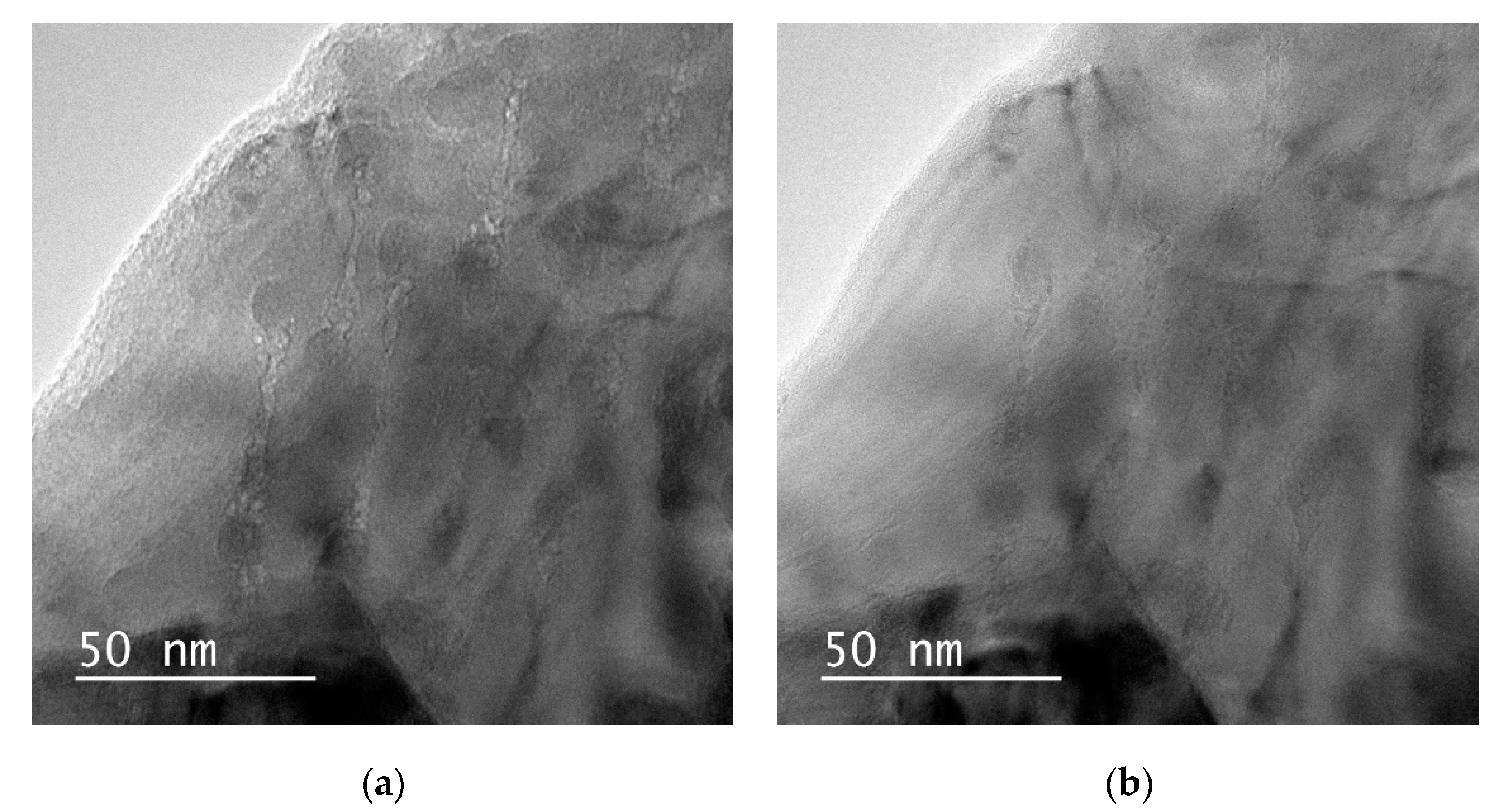
Figure 3a–c show magnified images of hillocks in LiNbO3, ZrSiO4, and GGG, respectively, irradiated with 200 MeV Au at an oblique incidence angle. As shown in the figures, hillocks are successfully observed in those materials. It is also found that the hillocks are clearly amorphous, which confirms the amorphizable nature of these ceramics. The side-view of the hillocks allows measuring both hillock diameter and height. The distribution of the hillock sizes is shown in Figure 2 together with that of the ion track sizes. The average sizes of the hillocks and track sizes are summarized in Table 1. As demonstrated in the table, the hillock diameter is always similar to the ion track size, although the former tends to be slightly larger than the latter. A hillock height seems nearly half of the hillock diameter.
3.2. Formation Process of Hillocks and Ion Tracks in LiNbO3, ZrSiO4, and GGG
The present study shows that both hillocks and ion tracks exhibit amorphous features, and they have similar sizes in amorphizable ceramics (LiNbO3, ZrSiO4, and GGG). The present results agree with the prediction of the thermal spike model. According to the thermal spike model, SHIs cause transient melting along the ion path, when the electronic stopping power exceeds a certain threshold value. During such transient melting, thermal pressure and volume change caused by solid-liquid transition lead to surface protrusion of the melt. In the amorphizable ceramics, rapid cooling after melting results in the formation of amorphous ion tracks and hillocks.
It is important to note that, although the hillock diameter appears to be similar to the ion track diameter, the magnified TEM images shows that the former is always slightly larger than the latter. This can be ascribed to the spreading tendency of a liquid on a solid surface. It is likely that the hillock shape is determined by the balance of the adhesive (the liquid wanting to maintain contact with the solid) and cohesive forces within the liquid (both internal cohesive force and surface tension) during melting. If the adhesive force dominates, the protruded part of the melt can spread over the surface, leading to the formation of bell-shaped hillocks. Conversely, it can turn into a spherical shape, if the cohesive force dominates. Such spherical hillocks have been reported in some ceramics irradiated with high-energy fullerene ions having a very high Se [50,51]. Large volume of surface protrusion induced by high Se may be closely related to the formation of spherical hillocks.
3.3. Hillocks and Ion Tracks in SrTiO3 and Nb-Doped SrTiO3
Figure 4 and Figure 5 show the bright field image of the ion tracks in STO and Nb-STO irradiated with 200 MeV Au at an oblique incidence angle, respectively. The ion track has a bright core surrounded by a dark fringe in the underfocus condition (Figure 4a and Figure 5a), whereas it has a dark core surrounded by a bright fringe in the overfocus condition (Figure 4b and Figure 5b). The Fresnel fringe is an indication of the formation of ion tracks with a lower density than that of the surrounding matrix [52,53]. Such focus-dependent Fresnel contrast is not found in amorphizable ceramics (e.g., YIG, LiNbO3, ZrSiO4, and GGG).
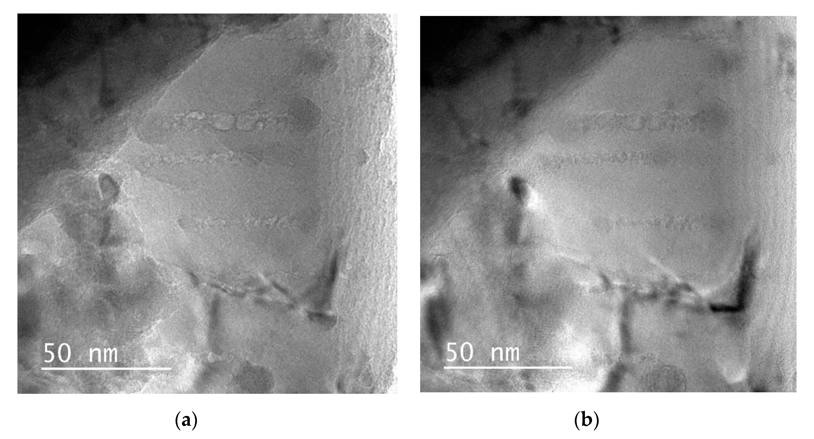
The ion tracks in STO and Nb-STO have inhomogeneous morphology in contrast to the homogenous morphology of the ion tracks in amorphizable ceramics. The inhomogeneity of the ion tracks is a common feature observed in non-amorphizable ceramics such as CeO2 [38], CaF2, SrF2, and BaF2 [36], in which partial recrystallization after transient melting is the likely cause of the inhomogeneous ion track formation. Black contrasts corresponding to hillocks are found at the end of the ion tracks. Figure 6 and Figure 7 show magnified images of a hillock created at the edge of the thin TEM samples of STO and Nb-STO, respectively. Bell-shaped hillocks are observed in STO and Nb-STO. In both materials, hillocks are found to be amorphous. It is interesting to find that amorphous hillocks are created, although the ion track region is recrystallized.
Since it is difficult to find inhomogeneous ion tracks in TEM, we could not find sufficient numbers of ion tracks and hillocks to perform a statistical analysis. Therefore, in this study, we only show the size range of ion tracks and hillocks observed in STO and Nb-STO in Table 2. As demonstrated in the table, there is a marked difference in the diameters of ion tracks and hillocks in both STO and Nb-STO. The large hillock diameter compared with the ion track diameter is also found in typical non-amorphizable ceramics (CaF2, SrF2, and BaF2). The present result can be a strong evidence that supports the recrystallization of the ion track regions in STO and Nb-STO. Conversely, the amorphous hillocks are signs of the failure of recrystallization. It seems that STO and Nb-STO are intermediate ceramics between amorphizable and non-amorphizable ceramics.
Here, it is important to discuss whether the ion tracks are actually crystalline or not, since some of the previous studies claimed that they are amorphous in STO. According to Ref. [54], analysis of X-ray diffraction peaks in ion-irradiated STO supports creation of amorphous ion tracks due to single impacts. In the same literature, although crystalline tracks containing defects are observed by TEM, the authors claimed that the crystalline tracks are created owing to 200 keV electron beam exposure which can cause amorphous–crystalline transition of ion track areas. Conversely, our TEM results of STO and Nb-STO support creation of crystalline ion tracks rather than amorphous ion tracks. For example, an inhomogenous feature of ion tracks in STO and Nb-STO is similar to that observed in partially recrystallized ion tracks in non-amorphizable ceramics. Moreover, the markedly smaller ion track diameter than the hillock diameter demonstrates that the ion track region is partially recrystallized after transient melting.
The clear difference in the morphology between the hillocks in STO and Nb-STO was not observed in this study. Therefore, the influence of Nb-doping on the hillock formation is not found in this study. A previous study using TEM and small angle X-ray scattering (SAXS) reported that 1 wt% Nb-doping does not affect track formation [55]. Track formation is easy in insulators since the energy of hot electrons is transferred to the lattice in insulators before being cooled down by free electrons. In contrast, track formation is difficult in metals since high electronic conductivity allows rapid energy diffusion in an electron subsystem. Although the electrical conductivity of Nb-STO is more than nine orders of magnitude higher than that of STO, the electron density may still be too low to influence the formation of hillocks and ion tracks. It should be noted that the electrical conductivity of metals is still much higher than that of Nb-STO. The difference of bonding character (metallic bonding in metals vs. ionic/covalent bonding in STO) should be also contributing to the less sensitivity of track formation in metals [55].
3.4. Factors That Determine the Recrystallization Process
The presence of recrystallization process separates non-amorphizable ceramics from amorphizable ceramics. Two factors that determine the recrystallization process have been proposed; (1) simplicity of lattice structure and (2) the strength of ionic bonding. The previous literature [15] proposed that a simple lattice structure with the smallest number of the peaks in the pair correlation function is in correlation with the recrystallization efficiency. Actually, amorphous ion tracks and hillocks are observed in YIG and GGG that have complicated crystal structure, whereas crystalline ion tracks and hillocks are observed in rather simple structured compounds (CaF2, SrF2, BaF2, and CeO2 with fluorite structure). STO has a relatively simple cubic structure with space group of Pmm, where there are only 5 atoms in the unit cell. The relatively simple crystal structure of STO can be the origin of the recrystallization of the ion track region. However, creation of amorphous hillocks in STO demonstrates that STO and Nb-STO are intermediate ceramics between amorphizable and non-amorphizable ceramics. Here, it is worth noting that STO has a perovskite structure which is composed of TiO2 planes and SrO planes, which make the structure somehow complicated. This unique structure of STO seems to be responsible for the intermediate behavior of ion-induced nanostructure formation. Therefore, we believe that the correlation of recrystallization effectiveness with the simplicity of the crystal structure is one of the promising hypotheses, and its validity should be further examined.
Another possible factor is the strength of ionic bonding, i.e., materials with a higher degree of ionicity recrystallize easily [19,56]. Non-amorphizable ceramics include many ionic crystals. It is conceivable that long-range ionic forces rather than short-range covalent interaction contribute to rapid recrystallization [19,57]. STO has mixed ionic-covalent bonding properties. While a hybridization of the O-2p states with the Ti-3d states within the TiO6 octahedra leads to a pronounced covalent bonding, Sr2+ and O2- ions exhibit an ionic bonding character. Although STO is one of the complex oxides, the ionic bonding character in STO may be also responsible for the partial recrystallization of ion tracks. Therefore, the two factors mentioned above is important to explain why STO and Nb-STO are intermediate ceramics between amorphizable and non-amorphizable ceramics.
It is worth discussing why the hillock region fail to recrystallize, whereas the ion track region recrystallizes in STO. The previous MD simulation demonstrated that oxygen atoms settle in their original sites faster than metal atoms in SHI-irradiated MgO and Al2O3, and metallic atoms then adjust to a layer of oxygen that has already been built [15]. The study concluded that that the ability of oxygen atoms to reach their equilibrium sites governs the recrystallization process after melting. It is conceivable that in STO, oxygen loss in the hillock region effectively hinders recovery of the lattice structure. The hillock region tends to be more oxygen deficient than the ion track region, since oxygen atoms tend to escape from the irradiated surface. An important role of oxygen deficiencies should be further investigated in the future.
3.5. Summary of Formation Processes of Hillocks and Ion Tracks
To understand the difference between nanostructure formation in amorphizable and non-amorphizable ceramics, it is important to describe the process in terms of melting and successive recrystallization.
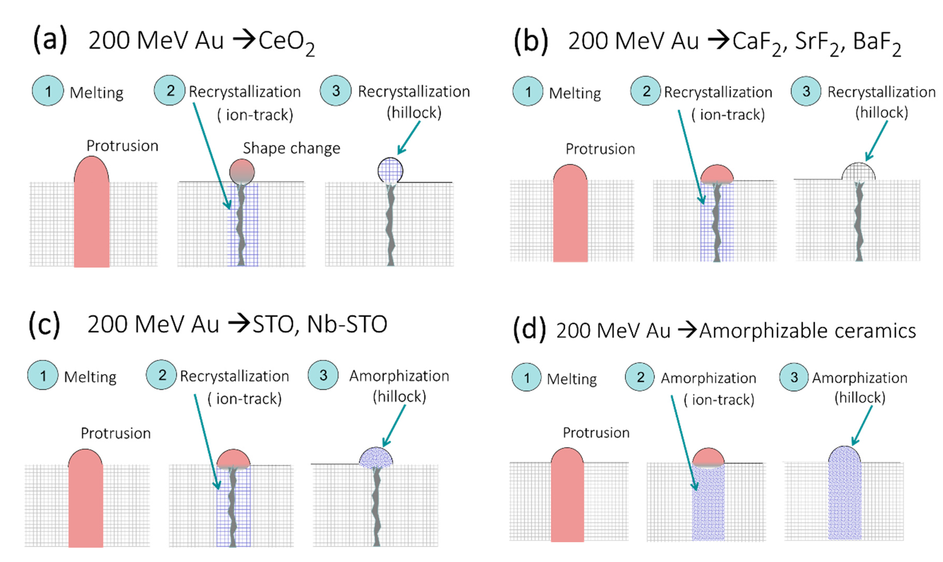
It is convenient to start the discussion with CeO2, which is one of the non-amorphizable ceramics. According to Ref. [38], hillocks are found to be spherical in CeO2 irradiated with 200 MeV Au. It was found that hillocks (spherical objects) have crystalline features, where the lattice orientation of hillocks was aligned with that of the matrix. This points out to the process consisting of the following three steps as explained in Figure 8a. (1) A molten region is created along the ion path. A part of the molten region protrudes above the surface because of the thermal pressure and additional pressure due to volume change caused by solid-liquid transition. (2) During cooling, the molten region embedded in the matrix begins to recrystallize. The partial recrystallization results in ion tracks smaller than those expected from the size of the melt. The shape change (spheroidization) of the protruded part strongly suggests that the protruded part remains liquid for a long period of time which is long enough for the molten protrusion to change its shape. The protruded part of the molten region can spheroidize if the surface tension is strong enough. (3) A droplet at the surface starts to recrystallize epitaxially using the matrix as a template lattice, so that a crystalline nanosphere having the same crystal orientation as that of the matrix is formed. This result strongly suggests that the molten region embedded in the matrix is solidified before the protruded part of the melt is solidified. It is reasonable to assume that this sequence of the solidification process applies to all SHI-irradiated ceramics. Such a sequence of solidification process is supported by the MD simulation of the nanostructure formation in CaF2 [16].
The likely process of nanostructure formation in fluorides (CaF2, SrF2, and BaF2) irradiated with 200 MeV Au is presented in Figure 8b. According to our previous study [36], most of the crystalline hillocks in these fluorides are nearly semispherical, although some of the hillocks have nearly spherical shape. Since recrystallization plays an important role in both fluorides and CeO2, the formation process in the fluorides should be similar to that of CeO2 (Figure 8a). The difference between the spherical shape of hillocks and non-spherical shape can be explained by the difference in volume of protrusion. If the volume of protrusion is large, the hillock shape tentatively has an unstable shape because of its high aspect ratio of height to width. It is conceivable that the unstable shape can rapidly turn into a stable spherical shape. Similar spherical hillocks have been already reported in some ceramics (Gd2Zr2O7 [50] and YIG [51]) irradiated with high-energy fullerene ions with very high Se, supporting the proposition that larger volume of the protrusion is the key to the formation of spherical hillocks.
The likely process of nanostructure formation in STO and Nb-STO is presented in Figure 8c. Although the first and second steps of the process in the figure are the same as those in Figure 8b, the third step of the process is different. Even though the molten region embedded in the matrix recrystallizes partially, the protruded part of the melt failed to recrystallize, resulting in amorphization. The failure of recrystallization only in the hillock region can be ascribed to oxygen deficiencies as discussed above.
The likely process in amorphizable ceramics (YIG, LiNbO3, ZrSiO4, and GGG) is presented in Figure 8d. The process consists of the following three steps. (1) A molten region is created along the ion path. A part of the molten region protrudes above the surface. (2) During cooling, the molten region embedded in the matrix starts to solidify, resulting in the amorphization of the molten region. Herein, the size of the molten region corresponds to that of the ion tracks. (3) The protruded part of the melt also starts to amorphize. This means that the hillock diameter is always similar to the ion track diameter. A subtle change of hillock shape leading to a slightly larger hillock diameter than the ion track diameter is not specified in the schematic, since this effect produces only a small difference between the hillock diameter and ion track diameter.
4. Conclusions
Amorphizable ceramics such as LiNbO3, ZrSiO4, and Gd3Ga5O12 were irradiated with 200 MeV Au ions at an oblique incidence angle. Line-like homogeneous ion tracks and bell-shaped hillocks are observed by TEM. The ion track and hillock diameters are similar for all the amorphizable ceramics, although the hillock diameter is found to be slightly larger than the ion track diameter. The TEM images of ion tracks in STO and Nb-STO irradiated with 200 MeV Au show similar features to those observed in the non-amorphizable ceramics. For example, the ion track diameter is markedly smaller than the hillock diameter, and they exhibit inhomogeneity. However, the hillocks in these ceramics are found to be amorphous which is in contrast to the crystalline feature of hillocks observed in the non-amorphizable ceramics. Therefore, it can be concluded that STO and Nb-STO are intermediate ceramics between amorphizable and non-amorphizable ceramics. No marked difference is observed between hillock formation in STO and that in Nb-STO. The material dependence of nanostructure formation can be ascribed to the intricate recrystallization process. The present results support that (1) simplicity of lattice structure and (2) the strength of ionic bonding can be the factors that determine the recrystallization effectiveness.
Author Contributions
Conceptualization, N.I.; TEM observation, N.I. and T.T.; Sample preparation, N.I.; Ion irradiation, N.I. and H.O.; Manuscript writing, N.I. All authors have read and agreed to the published version of the manuscript.
Funding
Part of the present work was financially supported by JSPS KAKENHI Grant Number 20K05389.
Acknowledgments
The authors are grateful to the technical staff of the tandem accelerator at JAEA-Tokai for supplying high-quality ion beams. One of the authors (N.I.) thanks A. Iwase and A. Kitamura for their constant support during the research.
Conflicts of Interest
The authors declare no conflict of interest.
References
- Toulemonde, M.; Assmann, W.; Dufour, C.; Meftah, A.; Trautmann, C. Nanometric transformation of the matter by short and intense electronic excitation: Experimental data versus inelastic thermal spike model. Nucl. Instrum. Methods Phys. Res. Sect. B Beam Interact. Mater. Atoms 2012, 277, 28–39. [Google Scholar] [CrossRef]
- Szenes, G. Comparison of two thermal spike models for ion–solid interaction. Nucl. Instrum. Methods Phys. Res. Sect. B Beam Interact. Mater. Atoms 2011, 269, 174–179. [Google Scholar] [CrossRef]
- Itoh, N.; Duffy, D.M.; Khakshouri, S.; Stoneham, A.M. Making tracks: Electronic excitation roles in forming swift heavy ion tracks. J. Phys. Condens. Matter 2009, 21, 474205. [Google Scholar] [CrossRef] [PubMed] [Green Version]
- Toulemonde, M.; Studer, F. Comparison of the radii of latent tracks induced by high-energy heavy ions in Y3Fe5O12 by HREM, channelling Rutherford backscattering and Mössbauer spectrometry. Philos. Mag. A 1988, 58, 799–808. [Google Scholar] [CrossRef]
- Toulemonde, M. Nanometric phase transformation of oxide materials under GeV energy heavy ion irradiation. Nucl. Instrum. Methods Phys. Res. Sect. B Beam Interact. Mater. Atoms 1999, 156, 1–11. [Google Scholar] [CrossRef]
- Szenes, G. Monoatomic and cluster ion irradiation induced amorphous tracks in yttrium iron garnet. Nucl. Instrum. Methods Phys. Res. Sect. B Beam Interact. Mater. Atoms 1998, 146, 420–425. [Google Scholar] [CrossRef]
- Szenes, G. Ion-velocity-dependent track formation in yttrium iron garnet: A thermal-spike analysis. Phys. Rev. B 1995, 52, 6154–6157. [Google Scholar] [CrossRef]
- Szenes, G. Information provided by a thermal spike analysis on the microscopic processes of track formation. Nucl. Instrum. Methods Phys. Res. Sect. B Beam Interact. Mater. Atoms 2002, 191, 54–58. [Google Scholar] [CrossRef]
- Toulemonde, M.; Dufour, C.; Meftah, A.; Paumier, E. Transient thermal processes in heavy ion irradiation of crystalline inorganic insulators. Nucl. Instrum. Methods Phys. Res. Sect. B Beam Interact. Mater. Atoms 2000, 166, 903–912. [Google Scholar] [CrossRef]
- Schwartz, K.; Trautmann, C.; Steckenreiter, T.; Geiß, O.; Krämer, M. Damage and track morphology in LiF crystals irradiated with GeV ions. Phys. Rev. B 1998, 58, 11232–11240. [Google Scholar] [CrossRef]
- Berthelot, A.; Hémon, S.; Gourbilleau, F.; Dufour, C.; Domengès, B. and Paumier, E. Behaviour of a nanometric SnO2 powder under swift heavy-ion irradiation: From sputtering to splitting. Phil. Mag. A 2000, 80, 2257. [Google Scholar] [CrossRef]
- Takaki, S.; Yasuda, K.; Yamamoto, T.; Matsumura, S.; Ishikawa, N. Structure of ion tracks in ceria irradiated with high energy xenon ions. Prog. Nucl. Energy 2016, 92, 306–312. [Google Scholar] [CrossRef]
- Toulemonde, M.; Benyagoub, A.; Trautmann, C.; Khalfaoui, N.; Boccanfuso, M.; Dufour, C.; Gourbilleau, F.; Grob, J.J.; Stoquert, J.P.; Costantini, J.M.; et al. Dense and nanometric electronic excitations induced by swift heavy ions in an ionic CaF2 crystal: Evidence for two thresholds of damage creation. Phys. Rev. B 2012, 85, 054112. [Google Scholar] [CrossRef] [Green Version]
- Toulemonde, M.; Assmann, W.; Dufour, C.; Meftah, A.; Studer, F.; Trautmann, C. Experimental Phenomena and Thermal Spike Model Description of Ion Tracks in Amorphisable Inorganic Insulators. Mat. Fys. Medd. 2006, 52, 263–292. [Google Scholar]
- Rymzhanov, R.A.; Medvedev, N.; O’Connell, J.H.; Van Vuuren, A.J.; Skuratov, V.A.; Volkov, A. Recrystallization as the governing mechanism of ion track formation. Sci. Rep. 2019, 9, 3837. [Google Scholar] [CrossRef] [PubMed]
- Rymzhanov, R.A.; O’Connell, J.; Van Vuuren, A.J.; Skuratov, V.A.; Medvedev, N.; Volkov, A. Insight into picosecond kinetics of insulator surface under ionizing radiation. J. Appl. Phys. 2020, 127, 015901. [Google Scholar] [CrossRef]
- Jiang, W.; Devanathan, R.; Sundgren, C.; Ishimaru, M.; Sato, K.; Varga, T.; Manandhar, S.; Benyagoub, A. Ion tracks and microstructures in barium titanate irradiated with swift heavy ions: A combined experimental and computational study. Acta Mater. 2013, 61, 7904–7916. [Google Scholar] [CrossRef]
- Zhang, J.; Lang, M.; Ewing, R.C.; Devanathan, R.; Weber, W.J.; Toulemonde, M. Nanoscale phase transitions under extreme conditions within an ion track. J. Mater. Res. 2010, 25, 1344–1351. [Google Scholar] [CrossRef]
- Trachenko, K. Understanding resistance to amorphization by radiation damage. J. Phys. Condens. Matter 2004, 16, R1491–R1515. [Google Scholar] [CrossRef]
- Aumayr, F.; Facsko, S.; El-Said, A.S.; Trautmann, C.; Schleberger, M. Single ion induced surface nanostructures: A comparison between slow highly charged and swift heavy ions. J. Phys. Condens. Matter 2011, 23, 393001. [Google Scholar] [CrossRef] [Green Version]
- El-Said, A.S.; Aumayr, F.; Della-Negra, S.; Neumann, R.; Schwartz, K.; Toulemonde, M.; Trautmann, C.; Voss, K.-O. Scanning force microscopy of surface damage created by fast C60 cluster ions in CaF2 and LaF3 single crystals. Nucl. Instrum. Methods Phys. Res. Sect. B Beam Interact. Mater. Atoms 2007, 256, 313–318. [Google Scholar] [CrossRef]
- Muller, C.; Voss, K.O.; Lang, M.; Neumann, R. Correction of systematic errors in scanning force microscopy images with application to ion track micrographs. Nucl. Instrum. Methods Phys. Res. Sect. B Beam Interact. Mater. Atoms 2003, 212, 318–325. [Google Scholar] [CrossRef]
- Popok, V.N.; Jensen, J.; Vuckovic, S.; Macková, A.; Trautmann, C. Formation of surface nanostructures on rutile (TiO2): Comparative study of low-energy cluster ion and high-energy monoatomic ion impact. J. Phys. D Appl. Phys. 2009, 42, 205303. [Google Scholar] [CrossRef]
- Meftah, A.; Benhacine, H.; Benyagoub, A.; Grob, J.; Izerrouken, M.; Kadid, S.; Khalfaoui, N.; Stoquert, J.; Toulemonde, M.; Trautmann, C. Data consistencies of swift heavy ion induced damage creation in yttrium iron garnet analyzed by different techniques. Nucl. Instrum. Methods Phys. Res. Sect. B Beam Interact. Mater. Atoms 2016, 366, 155–160. [Google Scholar] [CrossRef]
- Khalfaoui, N.; Rotaru, C.; Bouffard, S.; Toulemonde, M.; Stoquert, J.; Haas, F.; Trautmann, C.; Jensen, J.; Dunlop, A. Characterization of swift heavy ion tracks in CaF2 by scanning force and transmission electron microscopy. Nucl. Instrum. Methods Phys. Res. Sect. B Beam Interact. Mater. Atoms 2005, 240, 819–828. [Google Scholar] [CrossRef]
- Khalfaoui, N.; Rotaru, C.; Bouffard, S.; Jacquet, E.; Lebius, H.; Toulemonde, M. Study of swift heavy ion tracks on crystalline quartz surfaces. Nucl. Instrum. Methods Phys. Res. Sect. B Beam Interact. Mater. Atoms 2003, 209, 165–169. [Google Scholar] [CrossRef]
- Awazu, K.; Wang, X.; Fujimaki, M.; Komatsubara, T.; Ikeda, T.; Ohki, Y. Structure of latent tracks in rutile single crystal of titanium dioxide induced by swift heavy ions. J. Appl. Phys. 2006, 100, 044308. [Google Scholar] [CrossRef]
- Akcöltekin, E.; Akcöltekin, S.; Osmani, O.; Duvenbeck, A.; Lebius, H.; Schleberger, M. Swift heavy ion irradiation of SrTiO3 under grazing incidence. New J. Phys. 2008, 10, 53007. [Google Scholar] [CrossRef]
- Muller, C.; Cranney, M.; El-Said, A.; Ishikawa, N.; Iwase, A.; Lang, M.; Neumann, R. Ion tracks on LiF and CaF2 single crystals characterized by scanning force microscopy. Nucl. Instrum. Methods Phys. Res. Sect. B Beam Interact. Mater. Atoms 2002, 191, 246–250. [Google Scholar] [CrossRef]
- Skuratov, V.; Zagorski, D.; Efimov, A.E.; Kluev, V.; Toporov, Y.; Mchedlishvili, B. Swift heavy ion irradiation effect on the surface of sapphire single crystals. Radiat. Meas. 2001, 34, 571–576. [Google Scholar] [CrossRef]
- Schwen, D.; Bringa, E.M.; Krauser, J.; Weidinger, A.; Trautmann, C.; Hofsäss, H. Nano-hillock formation in diamond-like carbon induced by swift heavy projectiles in the electronic stopping regime: Experiments and atomistic simulations. Appl. Phys. Lett. 2012, 101, 113115. [Google Scholar] [CrossRef]
- Müller, A.; Müller, C.; Neumann, R.; Ohnesorge, F. Scanning force microscopy of heavy-ion induced damage in lithium fluoride single-crystals. Nucl. Instrum. Methods Phys. Res. Sect. B Beam Interact. Mater. Atoms 2000, 166, 581–585. [Google Scholar] [CrossRef]
- Ramos, S.; Bonardi, N.; Canut, B.; Bouffard, S.; Della-Negra, S. Damage creation in α-Al2O3 by MeV fullerene impacts. Nucl. Instrum. Methods Phys. Res. Sect. B Beam Interact. Mater. Atoms 1998, 143, 319–332. [Google Scholar] [CrossRef]
- Daya, D.B.; Hallén, A.; Eriksson, J.; Kopniczky, J.; Papaleo, R.; Reimann, C.; Håkansson, P.; Sundqvist, B.; Brunelle, A.; Della-Negra, S.; et al. Radiation damage features on mica and L-valine probed by scanning force microscopy. Nucl. Instrum. Methods Phys. Res. Sect. B Beam Interact. Mater. Atoms 1995, 106, 38–42. [Google Scholar] [CrossRef]
- Daya, D.B.; Hallén, A.; Håkansson, P.; Sundqvist, B.; Reimann, C. Scanning force microscopy study of surface tracks induced in mica by 78.2-MeV 127I ions. Nucl. Instrum. Methods Phys. Res. Sect. B Beam Interact. Mater. Atoms 1995, 103, 454–465. [Google Scholar] [CrossRef]
- Ishikawa, N.; Taguchi, T.; Okubo, N. Hillocks created for amorphizable and non-amorphizable ceramics irradiated with swift heavy ions: TEM study. Nanotechnology 2017, 28, 445708. [Google Scholar] [CrossRef]
- Ishikawa, N.; Taguchi, T.; Kitamura, A.; Szenes, G.; Toimil-Molares, M.E.; Trautmann, C. TEM analysis of ion tracks and hillocks produced by swift heavy ions of different velocities in Y3Fe5O12. J. Appl. Phys. 2020, 127, 055902. [Google Scholar] [CrossRef]
- Ishikawa, N.; Okubo, N.; Taguchi, T. Experimental evidence of crystalline hillocks created by irradiation of CeO2 with swift heavy ions: TEM study. Nanotechnology 2015, 26, 355701. [Google Scholar] [CrossRef]
- Karczewski, J.; Riegel, B.; Gazda, M.; Jasinski, P.; Kusz, B. Electrical and structural properties of Nb-doped SrTiO3 ceramics. J. Electroceramics 2009, 24, 326–330. [Google Scholar] [CrossRef]
- Ziegler, J.F.; Biersack, J.P.; Littmark, U. The Stopping and Range of Ions in Solids; Pergamon: New York, NY, USA, 1985. [Google Scholar]
- Ziegler, J.F. SRIM-2003. Nucl. Instrum. Methods B 2004, 219–220, 1027–1036. [Google Scholar] [CrossRef] [Green Version]
- Sachan, R.; Pakarinen, O.H.; Liu, P.; Patel, M.K.; Chisholm, M.F.; Zhang, Y.; Wang, X.L.; Weber, W.J. Structure and band gap determination of irradiation-induced amorphous nano-channels in LiNbO3. J. Appl. Phys. 2015, 117, 135902. [Google Scholar] [CrossRef]
- Canut, B.; Ramos, S.; Bonardi, N.; Chaumont, J.; Bernas, H.; Cottereau, E. Defect creation by MeV clusters in LiNbO3. Nucl. Instrum. Methods Phys. Res. Sect. B Beam Interact. Mater. Atoms 1997, 122, 335–338. [Google Scholar] [CrossRef]
- Canut, B.; Ramos, S.; Brenier, R.; Thevenard, P.; Loubet, J.; Toulemonde, M. Surface modifications of LiNbO3 single crystals induced by swift heavy ions. Nucl. Instrum. Methods Phys. Res. Sect. B Beam Interact. Mater. Atoms 1996, 107, 194–198. [Google Scholar] [CrossRef]
- Meftah, A.; Costantini, J.M.; Khalfaoui, N.; Boudjadar, S.; Stoquert, J.P.; Studer, F.; Toulemonde, M. Experimental determination of track cross-section in Gd3Ga5O12 and comparison to the inelastic thermal spike model applied to several materials. Nucl. Instrum. Methods B 2005, 237, 563–574. [Google Scholar] [CrossRef]
- Lang, M.; Lian, J.; Zhang, F.; Hendriks, B.W.; Trautmann, C.; Neumann, R.; Ewing, R.C. Fission tracks simulated by swift heavy ions at crustal pressures and temperatures. Earth Planet. Sci. Lett. 2008, 274, 355–358. [Google Scholar] [CrossRef]
- Bursill, L.A.; Braunshausen, G. Heavy-ion irradiation tracks in zircon. Philos. Mag. A 1990, 62, 395–420. [Google Scholar] [CrossRef]
- Costantini, J.; Miro, S.; Lelong, G.; Guillaumet, M.; Toulemonde, M. Damage induced in garnets by heavy ion irradiations: A study by optical spectroscopies. Philos. Mag. 2017, 98, 312–328. [Google Scholar] [CrossRef]
- Meftah, A.; Brisard, F.; Costantini, J.M.; Hage-Ali, M.; Stoquert, J.P.; Studer, F.; Toulemonde, M. Swift heavy ions in magnetic insulators: A damage-cross-section velocity effect. Phys. Rev. B 1993, 48, 920–925. [Google Scholar] [CrossRef]
- Zhang, J.; Lang, M.; Lian, J.; Liu, J.; Trautmann, C.; Della-Negra, S.; Toulemonde, M.; Ewing, R.C. Liquid-like phase formation in Gd2Zr2O7 by extremely ionizing irradiation. J. Appl. Phys. 2009, 105, 113510. [Google Scholar] [CrossRef]
- Jensen, J.; Dunlop, A.; Della-Negra, S.; Pascard, H. Tracks in YIG induced by MeV C60 ions. Nucl. Instrum. Methods Phys. Res. Sect. B Beam Interact. Mater. Atoms 1998, 135, 295–301. [Google Scholar] [CrossRef]
- Li, W.; Wang, L.; Sun, K.; Lang, M.; Trautmann, C.; Ewing, R.C. Porous fission fragment tracks in fluorapatite. Phys. Rev. B 2010, 82, 144109. [Google Scholar] [CrossRef] [Green Version]
- Karlušić, M.; Ghica, C.; Negrea, R.; Siketić, Z.; Jakšić, M.; Schleberger, M.; Fazinić, S. On the threshold for ion track formation in CaF2. New J. Phys. 2017, 19, 023023. [Google Scholar] [CrossRef] [Green Version]
- Grygiel, C.; Lebius, H.; Bouffard, S.; Quentin, A.; Ramillon, J.M.; Madi, T.; Guillous, S.; Been, T.; Guinement, P.; Lelièvre, D.; et al. Online in situ x-ray diffraction setup for structural modification studies during swift heavy ion irradiation. Rev. Sci. Instrum. 2012, 83, 13902. [Google Scholar] [CrossRef] [PubMed] [Green Version]
- Li, W.; Rodriguez, M.D.; Kluth, P.; Lang, M.; Medvedev, N.; Sorokin, M.; Zhang, J.; Afra, B.; Bender, M.; Severin, D.; et al. Effect of doping on the radiation response of conductive Nb–SrTiO3. Nucl. Instrum. Methods Phys. Res. Sect. B Beam Interact. Mater. Atoms 2013, 302, 40–47. [Google Scholar] [CrossRef] [Green Version]
- Lang, M.; Djurabekova, F.; Medvedev, N.; Toulemonde, M.; Trautmann, C. Fundamental Phenomena and Applications of Swift Heavy Ion Irradiations Comprehensive Nuclear Materials (Second Edition). arXiv 2020, arXiv:2001.03711. [Google Scholar]
- Sattonnay, G.; Thome, L.; Sellami, N.; Monnet, I.; Grygiel, C.; Legros, C.; Tétot, R. Experimental approach and atomistic simulations to investigate the radiation tolerance of complex oxides: Application to the amorphization of pyrochlores. Nucl. Instrum. Methods Phys. Res. Sect. B Beam Interact. Mater. Atoms 2014, 326, 228–233. [Google Scholar] [CrossRef]
Figure 1.
Bright field images of ion tracks induced in (a) LiNbO3, (b) ZrSiO4, and (c) Gd3Ga5O12 irradiated with 200 MeV Au32+ at an oblique incidence angle. The images were taken at relatively low magnification.
Figure 1.
Bright field images of ion tracks induced in (a) LiNbO3, (b) ZrSiO4, and (c) Gd3Ga5O12 irradiated with 200 MeV Au32+ at an oblique incidence angle. The images were taken at relatively low magnification.

Figure 2.
Size distribution of the track diameter, the hillock diameter, and the hillock height in (a) LiNbO3, (b) ZrSiO4, and (c) Gd3Ga5O12 irradiated with 200 MeV Au32+ at an oblique incidence angle.
Figure 2.
Size distribution of the track diameter, the hillock diameter, and the hillock height in (a) LiNbO3, (b) ZrSiO4, and (c) Gd3Ga5O12 irradiated with 200 MeV Au32+ at an oblique incidence angle.

Figure 3.
Bright field images of hillocks induced in (a) LiNbO3, (b) ZrSiO4, and (c) Gd3Ga5O12 irradiated with 200 MeV Au32+ at an oblique incidence angle. The images were taken at relatively high magnification.
Figure 3.
Bright field images of hillocks induced in (a) LiNbO3, (b) ZrSiO4, and (c) Gd3Ga5O12 irradiated with 200 MeV Au32+ at an oblique incidence angle. The images were taken at relatively high magnification.

Figure 4.
Bright field images of ion tracks induced in SrTiO3 irradiated with 200 MeV Au32+ at an oblique incidence angle. The images were taken in (a) underfocus and (b) overfocus conditions.
Figure 4.
Bright field images of ion tracks induced in SrTiO3 irradiated with 200 MeV Au32+ at an oblique incidence angle. The images were taken in (a) underfocus and (b) overfocus conditions.

Figure 5.
Bright field images of ion tracks induced in Nb-doped SrTiO3 irradiated with 200 MeV Au32+ at an oblique incidence angle. The images were taken in (a) underfocus condition and (b) overfocus condition.
Figure 5.
Bright field images of ion tracks induced in Nb-doped SrTiO3 irradiated with 200 MeV Au32+ at an oblique incidence angle. The images were taken in (a) underfocus condition and (b) overfocus condition.

Figure 6.
Bright field images of hillocks induced in SrTiO3 irradiated with 200 MeV Au32+ at an oblique incidence angle.
Figure 6.
Bright field images of hillocks induced in SrTiO3 irradiated with 200 MeV Au32+ at an oblique incidence angle.

Figure 7.
Bright field images of hillocks induced in Nb-doped SrTiO3 irradiated with 200 MeV Au32+ at an oblique incidence angle.
Figure 7.
Bright field images of hillocks induced in Nb-doped SrTiO3 irradiated with 200 MeV Au32+ at an oblique incidence angle.

Figure 8.
Schematic formation processes of ion tracks and hillocks in (a) CeO2, (b) fluorides (CaF2, SrF2, and BaF2), (c) STO and Nb-STO, and (d) amorphizable ceramics (YIG, LiNbO3, ZrSiO4, and GGG).
Figure 8.
Schematic formation processes of ion tracks and hillocks in (a) CeO2, (b) fluorides (CaF2, SrF2, and BaF2), (c) STO and Nb-STO, and (d) amorphizable ceramics (YIG, LiNbO3, ZrSiO4, and GGG).


Table 1.
Average diameter of ion tracks (Dtrack), average diameter of hillocks (Dhillock), average height of hillocks (Hhillock) are listed with standard deviations for LiNbO3, ZrSiO4, and GGG irradiated with 200 MeV Au32+. The corresponding Se values are also listed.
Table 1.
Average diameter of ion tracks (Dtrack), average diameter of hillocks (Dhillock), average height of hillocks (Hhillock) are listed with standard deviations for LiNbO3, ZrSiO4, and GGG irradiated with 200 MeV Au32+. The corresponding Se values are also listed.
| Dtrack (nm) | Dhillock (nm) | Hhillock (nm) | Se (keV/nm) | |
|---|---|---|---|---|
| LiNbO3 | 11.7 ± 1.3 | 13.2 ± 1.5 | 5.8 ± 1.2 | 28.1 |
| ZrSiO4 | 9.5 ± 0.5 | 11.6 ± 1.1 | 5.3 ± 0.8 | 29.6 |
| GGG | 11.3 ± 0.9 | 14.7 ± 2.0 | 4.7 ± 1.0 | 34.2 |
Table 2.
Approximate values of ion track diameter (Dtrack), hillock diameter (Dhillock), and hillock height (Hhillock) in SrTiO3 (STO) and 0.5 wt% niobium-doped STO (Nb-STO). The corresponding Se values are also listed.
Table 2.
Approximate values of ion track diameter (Dtrack), hillock diameter (Dhillock), and hillock height (Hhillock) in SrTiO3 (STO) and 0.5 wt% niobium-doped STO (Nb-STO). The corresponding Se values are also listed.
| Dtrack (nm) | Dhillock (nm) | Hhillock (nm) | Se (keV/nm) | |
|---|---|---|---|---|
| STO | 3~5 | 12~15 | 4~5 | 28.6 |
| Nb-STO | 3~4 | 11~13 | 4~5 | 28.5 |
Publisher’s Note: MDPI stays neutral with regard to jurisdictional claims in published maps and institutional affiliations. |
© 2020 by the authors. Licensee MDPI, Basel, Switzerland. This article is an open access article distributed under the terms and conditions of the Creative Commons Attribution (CC BY) license (http://creativecommons.org/licenses/by/4.0/).
Share and Cite
MDPI and ACS Style
Ishikawa, N.; Taguchi, T.; Ogawa, H. Comprehensive Understanding of Hillocks and Ion Tracks in Ceramics Irradiated with Swift Heavy Ions. Quantum Beam Sci. 2020, 4, 43. https://0-doi-org.brum.beds.ac.uk/10.3390/qubs4040043
AMA Style
Ishikawa N, Taguchi T, Ogawa H. Comprehensive Understanding of Hillocks and Ion Tracks in Ceramics Irradiated with Swift Heavy Ions. Quantum Beam Science. 2020; 4(4):43. https://0-doi-org.brum.beds.ac.uk/10.3390/qubs4040043
Chicago/Turabian StyleIshikawa, Norito, Tomitsugu Taguchi, and Hiroaki Ogawa. 2020. "Comprehensive Understanding of Hillocks and Ion Tracks in Ceramics Irradiated with Swift Heavy Ions" Quantum Beam Science 4, no. 4: 43. https://0-doi-org.brum.beds.ac.uk/10.3390/qubs4040043