Self-Organized Nanostructures Generated on Metal Surfaces under Electron Irradiation


Department of Physics, Hyogo University of Teacher Education, Kato 673-1494, Hyogo, Japan
Quantum Beam Sci. 2021, 5(1), 4; https://0-doi-org.brum.beds.ac.uk/10.3390/qubs5010004
Submission received: 3 December 2020
/
Revised: 14 January 2021
/
Accepted: 14 January 2021
/
Published: 19 January 2021
(This article belongs to the Special Issue The Modifications of Metallic and Inorganic Materials by Using Energetic Ion/Electron Beams)
Abstract
:Irradiation of high-energy electrons can produce surface vacancies on the exit surface of thin foils by the sputtering of atoms. Although the sputtering randomly occurs in the area irradiated with an intense electron beam of several hundred nanometers in diameter, characteristic topographic features can appear under irradiation. This paper reviews a novel phenomenon on a self-organization of nanogrooves and nanoholes generated on the exit surface of thin metal foils irradiated with high doses of 360–1250 keV electrons. The phenomenon was discovered firstly for gold irradiated at temperatures about 100 K, which shows the formation of grooves and holes with widths between 1 and 2 nm. Irradiation along [001] produces grooves extending along [100] and [010], irradiation along [011] gives grooves along [100], whereas no clear grooves have been observed for [111] irradiations. By contrast, nanoholes, which may reach depths exceeding 20 nm, develop mainly along the beam direction. The formation of the nanostructures depends on the irradiation temperatures, exhibiting an existence of a critical temperature at about 240 K, above which the width significantly increases, and the density decreases. Nanostructures formed for silver, copper, nickel, and iron were also investigated. The self-organized process was discussed in terms of irradiation-induced effects.
1. Introduction
Generation of nanosized structures is technologically important, and the controlled formation of structures in solids on a nanometer scale is critical to modern technology [1,2,3]. Such structures may have properties different from those of the bulk materials. Nanohole-based nanomaterials with a size less than the wavelength of an excitation laser beam, for example, are promised for applications such as chemical and biological sensing, membrane biorecognition, unique optical responses under laser excitation, etc.
It should be worthwhile to know the smallest size of nanostructured material. The scanning tunneling microscope has been employed to control the deposition of atoms on or extraction of atoms from the surface on an atomic scale [4,5,6]. However, there seems to be a minimum width when one tries to produce deep nanoholes or nanogrooves.
High-energy particle irradiation is one of method to generate interesting nanomaterials [7,8]. Aggregation of surface vacancies produced homogeneously by ion sputtering may produce pits that can become rather deep. Electron irradiation, which can induce back sputtering on the surface of thin foil specimens, is also one of the techniques used for nanometer scale etching, lithography and hole formation, and intense convergent electron beams have been utilized, so far. Deep nanoholes have been formed in MgO using a convergent nanosized electron beam, the smallest widths so far achieved being about 1 nm [9,10]. Parallel electron beams, on the other hand, of 500–1000 nm diameter have been shown to produce pits on the exit surface of Au(111) foils by sputtering over the electron energy range of 0.4–1.1 MeV [11].
Self-organization is one method to produce characteristic structures and several self-organization phenomena of defect clusters under high-energy particle irradiations such as voids, bubbles, and stacking fault tetrahedra have been reported so far [12,13,14,15,16]. Spontaneous well-ordered periodicity can be developed on a broad surface by ion beam sputtering and a numerical model has been proposed as the formation process [17].
The present paper reviews our studies on the evolution of nanosized structures resulting from the sputtering of atoms from the exit surface of thin metal specimens during homogeneous electron irradiation, focusing on a novel self-organization phenomenon, which can occur on the electron irradiated surface [18,19,20,21,22] and give additional data on the temperature dependence of the formation of nanoholes for gold.
2. Materials and Methods
In the present study, we used the wedge-shaped specimens produced from 99.998% Au, 99.9999% Ag, 99.999% Cu, 99.998% Ni, and 99.997% Fe foils with a thickness of about 100 μm. After eliminating lattice defects by annealing, they were thinned by jet-polishing to make wedge-shaped specimens. The electron irradiations were performed by using two transmission electron microscopes (TEM) of JEOL-ARM 1250 and JEOL-4000FX, both equipped with GATAN liquid-nitrogen cooling stages.
The irradiations were done along crystallographic directions near the [100], [110], or [111] direction of grains with surface orientations near {100}, using a beam of about 200–800 nm diameter as illustrated in Figure 1 and a flux density of about 1024 electrons m−2 s−1 with total fluences ranging from 1027 to 1028 electrons m−2. The irradiation direction was adjusted by tilting the specimen. Although the surface orientation and the observation directions were not perfectly aligned with the crystallographic orientations in question, such crystallographic indices are used hereafter to show the surface orientation and observation directions. The irradiation time ranged from several 10 s to several 1000 s. A small fraction of incident electrons (10−6 for 1.0 MeV electrons) can give sufficient energy with target atoms on the electron exit surface to cause sputtering [23]. The electron microscopy observations were made with strongly reduced beam currents to suppress additional sputtering. Detailed experimental and theoretical study on the sputtering yield and angular distribution of sputtered atoms, among others, for gold foils in a high-voltage electron microscope have been given by Cherns et al. [23].
3. Results
3.1. Gold
3.1.1. Self-Organization of Nanostructure
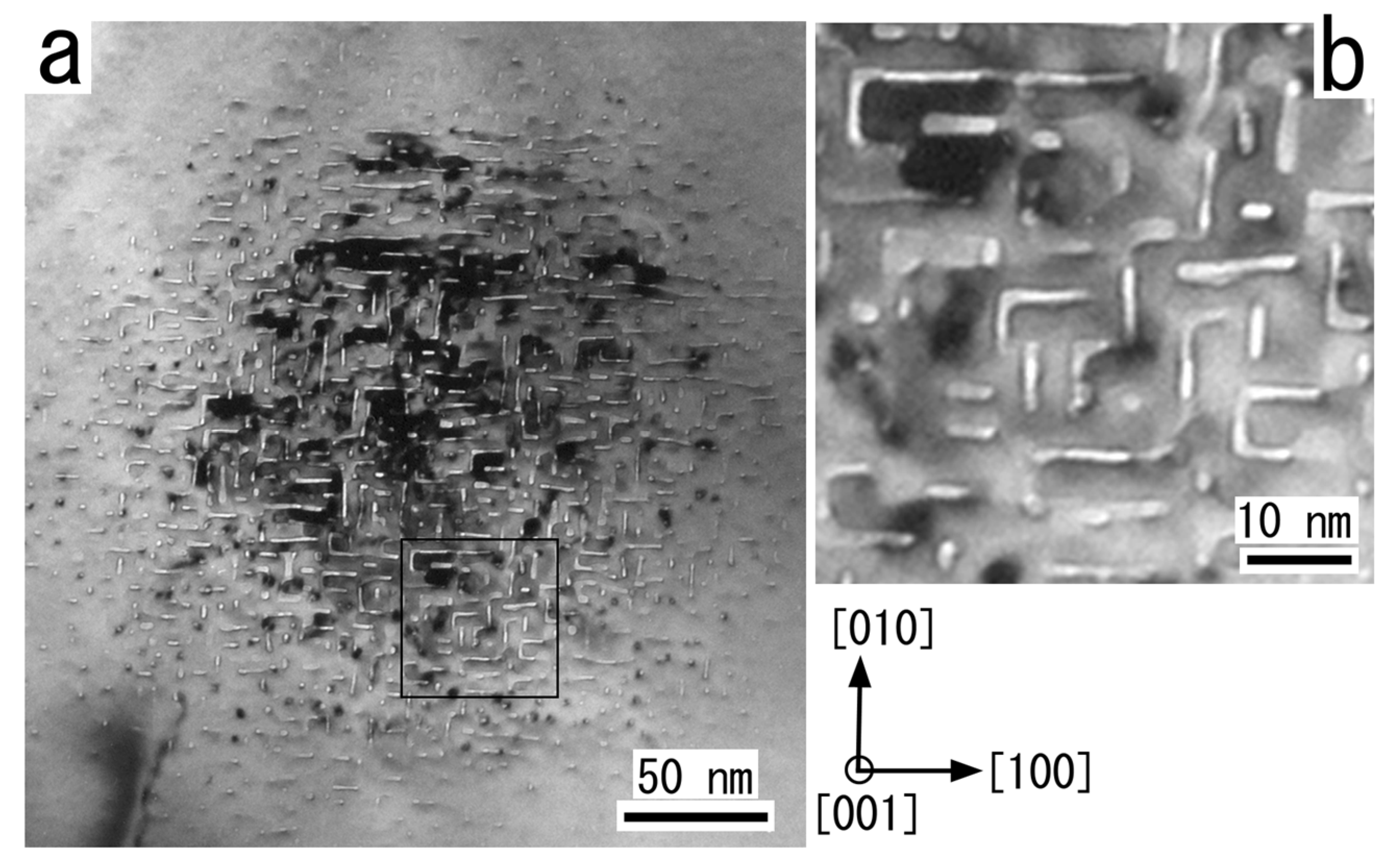
Figure 2 shows a typical self-organized pattern observed for an Au(001) foil irradiated with 400 keV electrons along [001] direction at 95 K with an electron beam of about 300 nm in diameter. The micrograph was taken under a kinematic and slightly under-focus condition. Clear bright images extending along [100] and [010] with a width of 1–2 nm can be observed. Stereomicroscopy revealed that these bright lines are grooves formed on the electron exit surface.
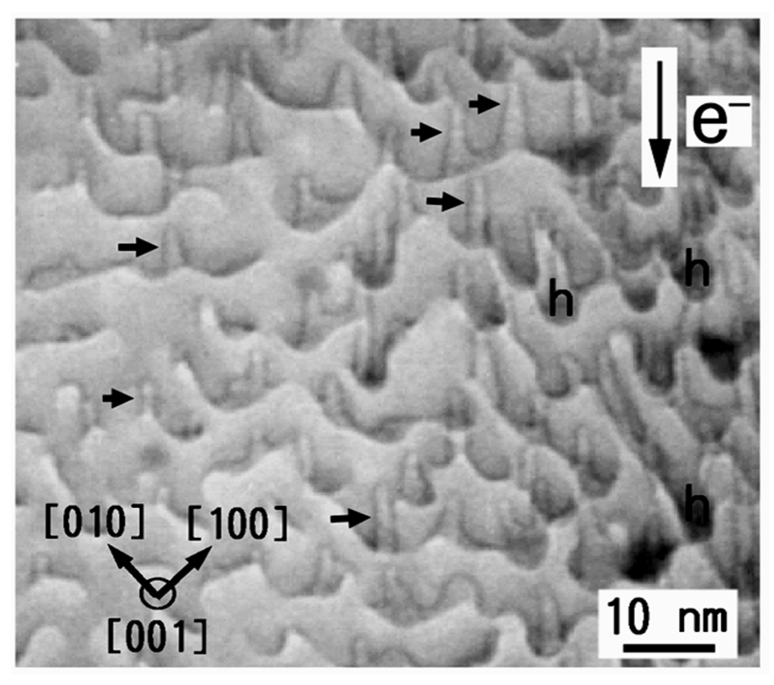
Figure 3 shows an oblique observation of an Au(001) foil, which was irradiated along [112] with 400 keV electrons at 95 K and observed along [001] by tilting the specimen. Deep nanoholes and hillocks formed on the exit surface of an Au(001) foil can be seen. Aspect ratio on the nanohole is very high in spite of the small diameter of 1–2 nm.
3.1.2. Irradiation Directional Dependence on the Structure
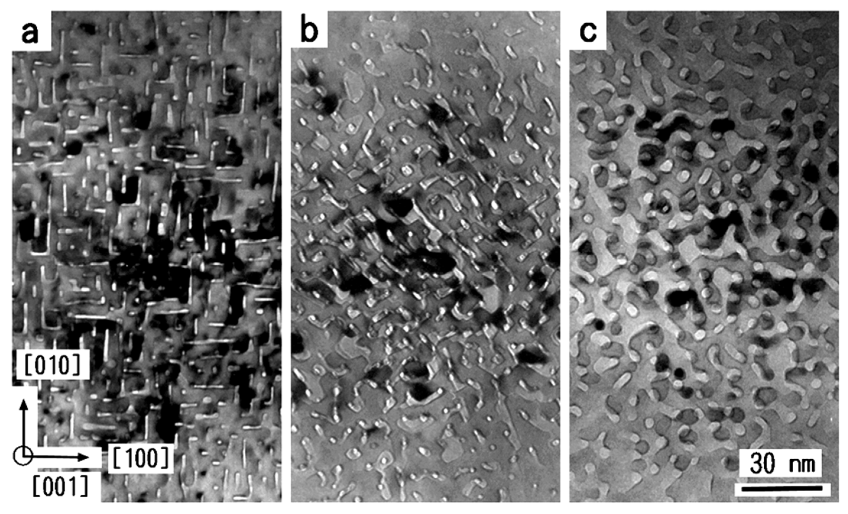
Figure 4a–c exhibit TEM images obtained under kinematic and slightly under-focus conditions for a (001)-oriented foil after irradiation with 800 keV electrons at 110 K to a fluence of 8 × 1026 electrons m−2, which were, respectively, irradiated along [001], [011] and [111] directions. Stereomicroscopy indicated that the elongated bright contrasts along [001] and [010] for the [001] irradiation were due to grooves at the electron exit surface of the foil. Different results were obtained after the irradiations along [011] or [111] directions, as seen in Figure 4b,c, respectively. We can find bright contrasts extending along [100] for [011] irradiation, which are due to grooves but cannot find groove formation after [111] irradiation. The white contrasts in Figure 4c are caused by pits. These results suggest strongly that the groove formation is affected by the angle between the beam direction and the surface normal.
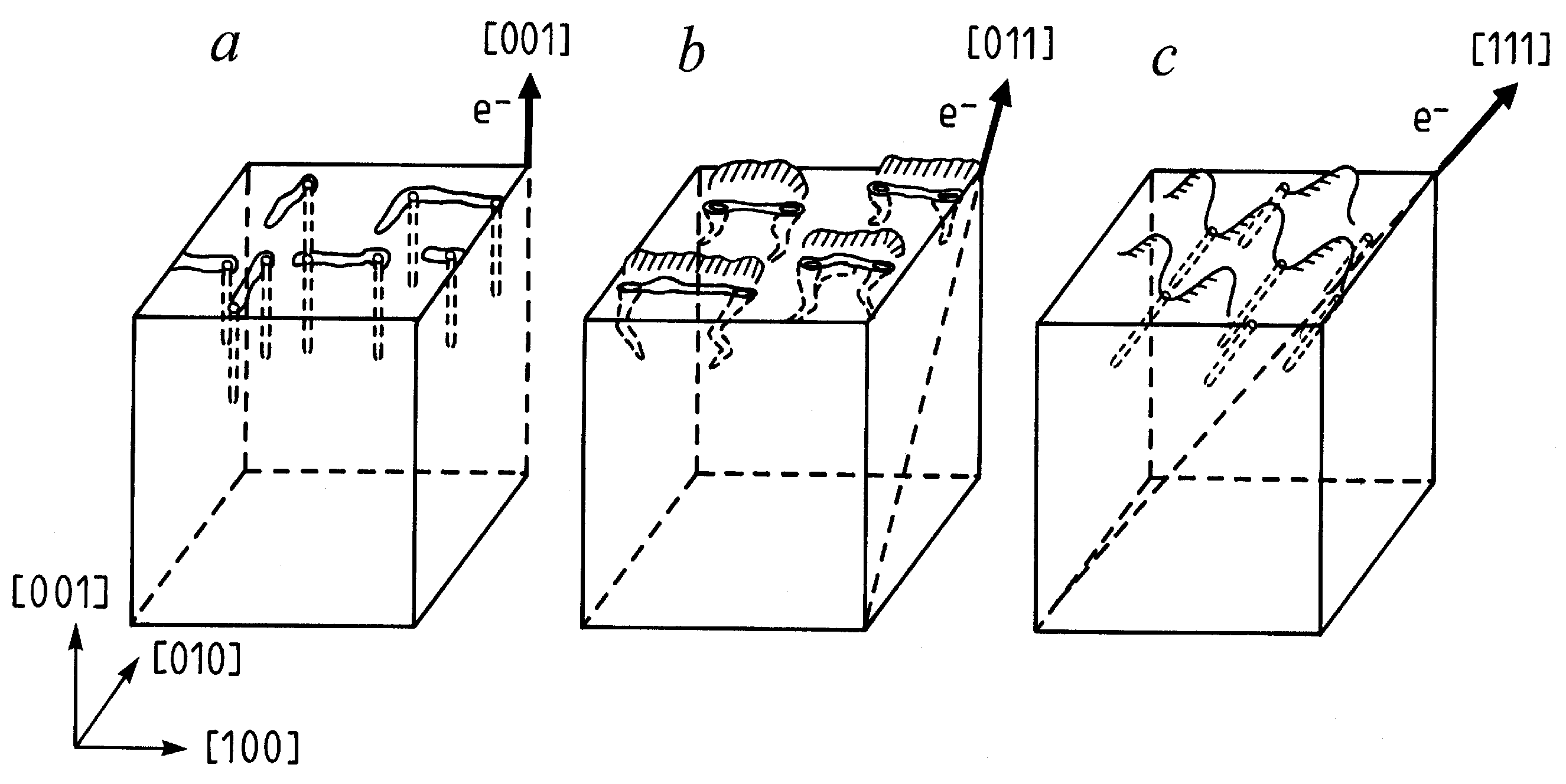
A detailed analysis has led us to schematic pictures on the nanostructure formed on the exit surface of gold films under electron irradiation as shown in Figure 5 [18]. The sputtered structure mainly consists of anisotropic nanogrooves, deep nanoholes, and hillocks. No clear grooves appear for the [111] irradiation. The nanoholes grow parallel to the irradiation direction both under [001] and [111] irradiations without much change in their widths but are zigzagged under [011] irradiation. Note the large aspect ratio of these nanoholes with extremely small dimension; the width and depth of the smallest nanoholes formed by the [111] irradiation, for example, are about 1.5 nm and more than 20 nm, respectively. In all three cases, the hillocks develop along the irradiation directions, although not indicated in Figure 5a for clarity.
Similar results were obtained for the groove and pit formation for 1250 keV electron irradiation of an Au(001) foil at 110 K. However, additionally, the formation of stacking-fault tetrahedra were observed, corresponding well to the estimated threshold electron energy of about 1150 keV for the Frenkel pair production in gold at 110 K [24].
3.1.3. Generation of Nanoslits and Nanoparticles
Successive sputtering due to electron irradiation induces thinning of the specimen, finally leading to the penetration of thin foils from the exit to the incident surfaces by nanogrooves and nanoholes. Figure 6a–d show the development of the nanostructure for an Au(011) foil irradiated with 400 keV electrons along [011] at 95 K. We can see that the width of nanogrooves in the pattern, which appeared in the initial stage of irradiation does not change significantly under irradiation. In Figure 6c, the penetration occurred in an area near the beam center, and then, nanoslits were formed as denoted by an arrow. In Figure 6d, the nanoslit denoted by the arrow in Figure 6c is closed, making the nanoslits beside it wider. This means the nanoslit became unstable under irradiation, probably due to its small size.
The self-organized pattern of nanoslits is seen to be determined in the initial stage of irradiation. Nanogrooves tend to develop along [100] direction, finally forming nanowires between the grooves. This method of the formation of nanowires using electron-beam irradiation in an electron microscope has been used to investigate characteristic nanostructures, which can appear in small size such as nanowires stabilized by the hcp lattices of the surfaces [25] and the ones consisting of helical atom rows coiled round the wire axis [26].
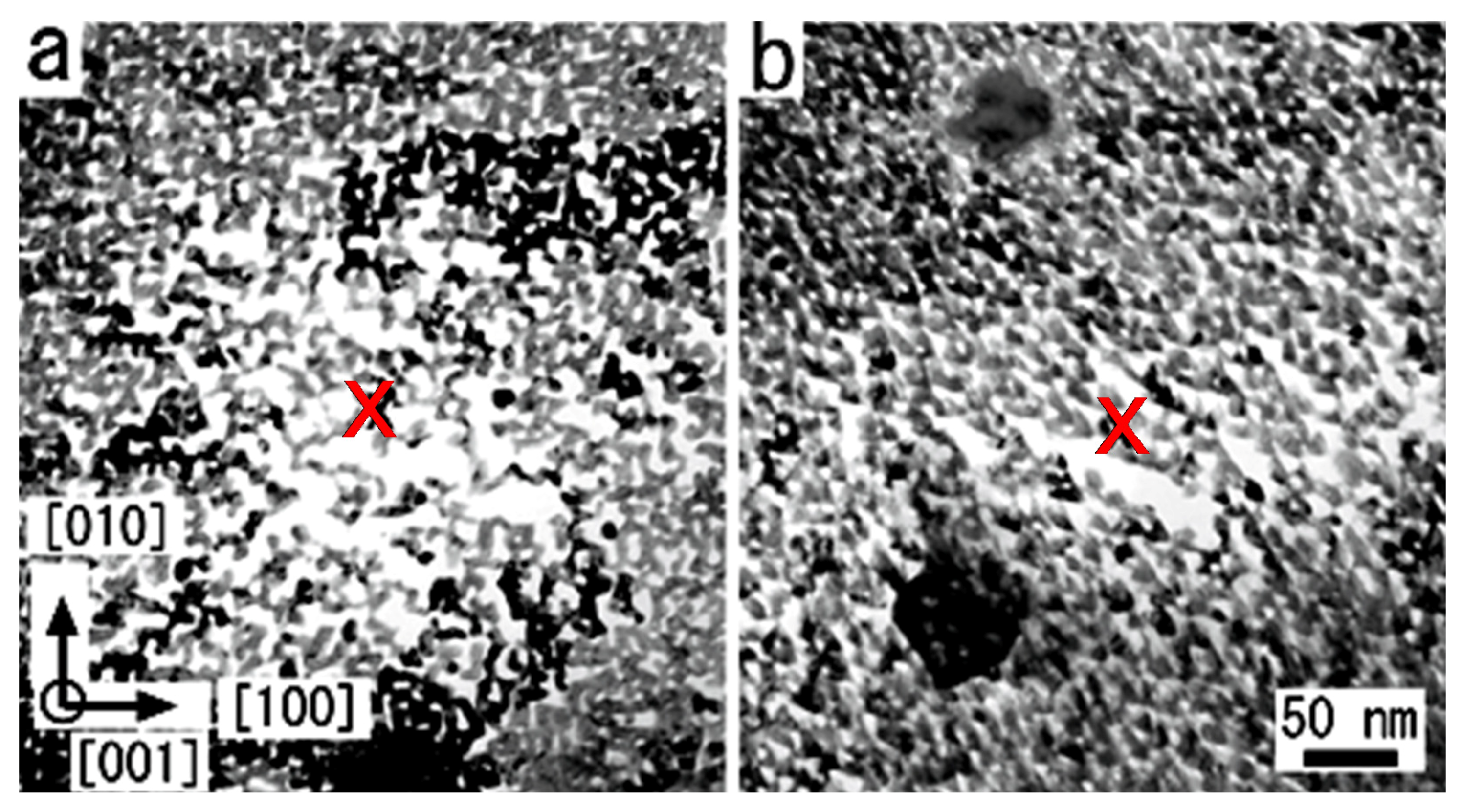
Figure 7a,b, respectively, show nanostructures of Au(001) foils irradiated with 1.25 MeV electrons at 110 K along [001] and [111] directions. The structures near the beam center denoted by X are seen to be pierced with a lot of holes produced by the irradiation and nanoparticles connected to each other. The shape of nanoparticles seen in Figure 7a,b reflects the self-organized nanostructures seen in Figure 4a,c, respectively. This method of particle formation may be useful for investigating the dependence of the characteristics of nanosized particle on size due to two advantages; one is the continuous preparation of a fresh surface under sputtering, and the other is the unique method of particle generation from thin foils.
3.1.4. Annealing of the Nanostructure at Room Temperature
Figure 8a,b, respectively, show an area of Au foil irradiated along [111] at 800 keV with a fluence of about 8 × 1026 electrons m−2 and annealed at room temperature. Both the photos were observed obliquely from [001] direction, by tilting the specimen from the irradiation direction. The projection of the electron-beam direction during irradiation is indicated by an arrow in Figure 8a, and nanoholes are observed with parallel dark lines. They appear to develop rather randomly under [011] irradiation but grow along the irradiation direction under [111] irradiation [18]. The dark features are hillocks developing along the irradiation directions. On room-temperature annealing, the nanoholes become thermally unstable irrespective of the original irradiation direction. They transform to voids with large diameters, while the hillocks decrease in height, as seen in Figure 8b.
3.1.5. Irradiation Temperature Dependence on the Structure
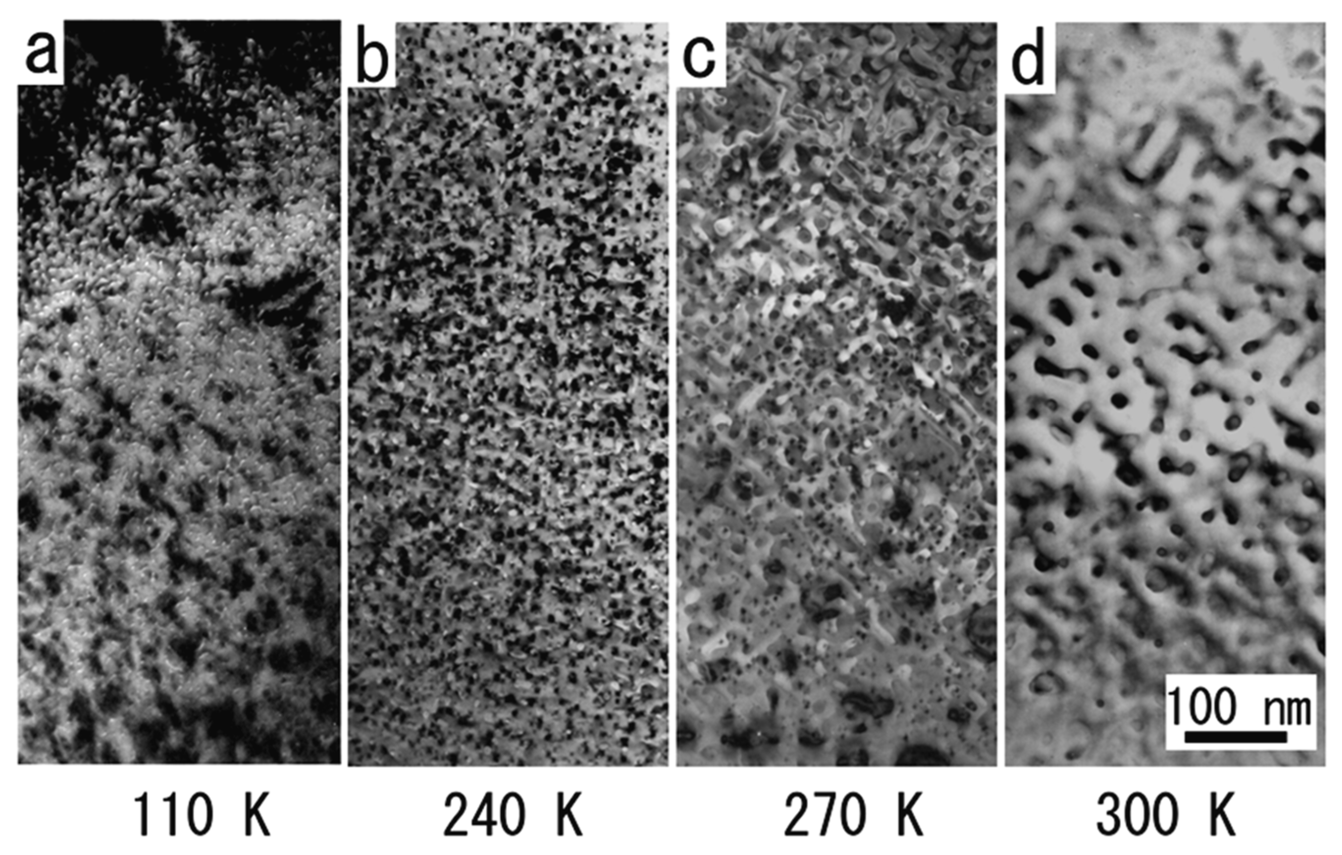
To know the irradiation temperature dependence on the formation of nanostructure, we investigated the structural change under electron irradiation at several different temperatures. Figure 9 shows bright-field images of Au(001) foils irradiated along [001] direction at four different temperatures. The electron irradiations were done with a beam of several hundred nm in diameter, and observation were done in areas where the structure looks homogeneous. The flux density is about 2 × 1024 electrons m−2 s−1.
Nanoholes formed by the irradiations are observed as bright circular images in Figure 9a,b and dark circular images in Figure 9c,d. One should note that the density of nanohole is almost constant over the irradiated dose range at each irradiation temperature [11]. Then, the difference in the time indicated in Figure 9 does not significantly affect the investigation on the temperature dependence of the density of nanoholes.
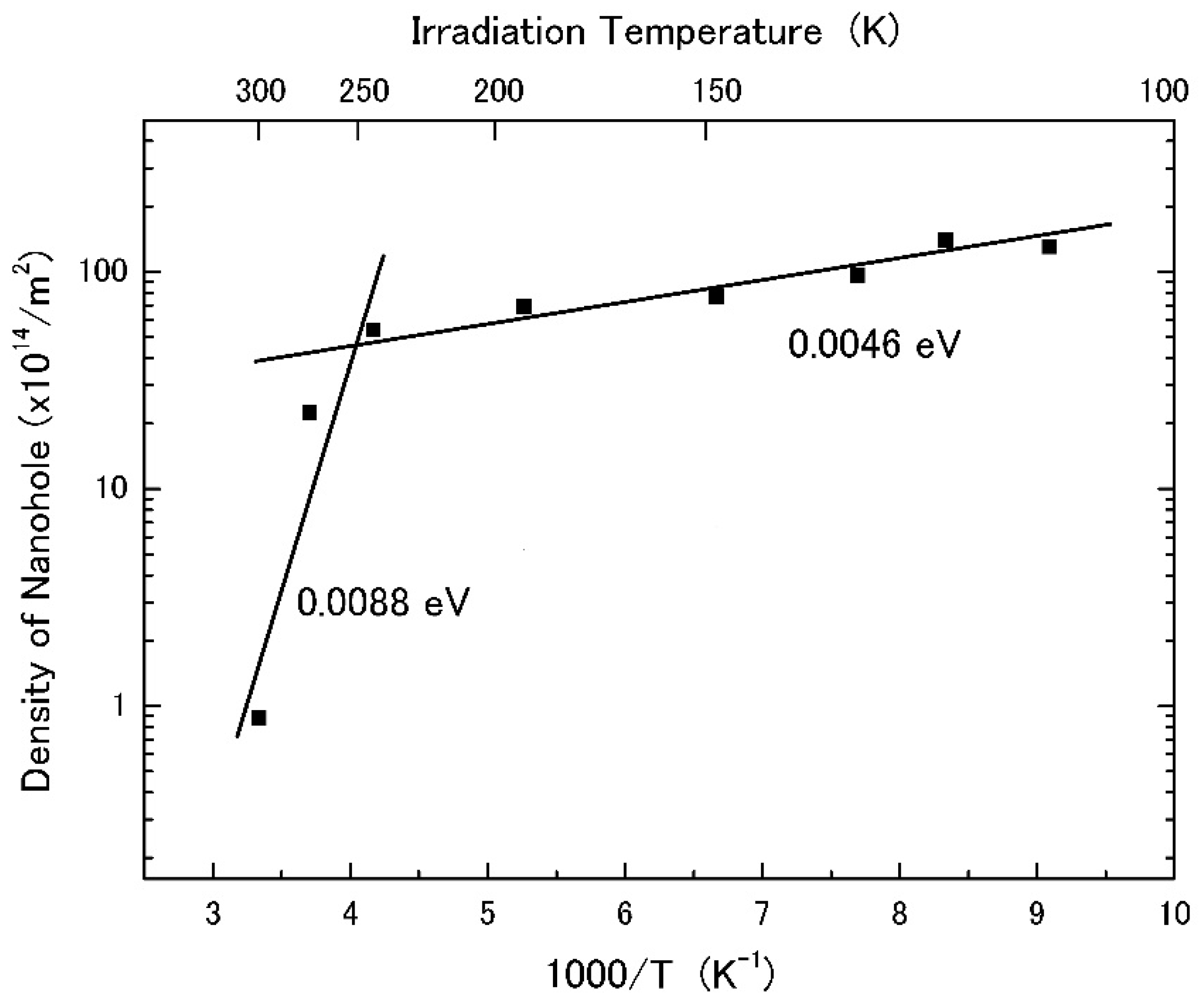
Figure 10 shows the Arrhenius plot of the density of nanoholes. We can find two lines with apparent activation energy of 0.0046 eV below 240 K and 0.088 eV above 240 K. Similar studies were done several decades ago by Cherns [11]. He gave in situ observation of sputtering at 1.0 MeV with thin (111) gold films by using the Harwell EM7 high-voltage electron microscope. He measured the pit density, which corresponds to the nanohole density in the present study, against the irradiation temperature and found a temperature dependence on the pit density. However, he could not measure the pit densities greater than about 1–2 ×10¹⁶ m−2, owing to a limit in the image resolution between adjacent pits. In the present study, we used JEOL-1250 transmission electron microscope, and the resolution is enough high to determine the density below 273 K, as seen in Figure 10.
Cherns proposed a theoretical model in which pits form by the diffusion and agglomeration of surface vacancies produced by sputtering. The model explains the experimental results in some detail, and the apparent activation energy of pit density against 1/T is suggested to take a value of Em/3, where Em is the migration energy of surface vacancy. Utilizing Cherns’ model in the present result on the density of pits on Au(001), the migration energy of a surface vacancy on Au(001) is derived to be 0.26 eV with the apparent activation energy of 0.088 eV shown in Figure 10. The value is lower than Em = 0.45 eV given by Cherns, but almost in the range of error bar. If the apparent activation energy of 0.088 eV above 240 K were to relate to the migration of vacancy, a following question remains; “what is the activation process for the lower value of 0.0046 eV below 240 K?”, which has not been found by Cherns. We can guess that the activation energy below 240 K may relate to the migration of adatom, etc., but further experimental and theoretical studies are awaited.
3.2. Comparison among Gold, Silver, and Copper
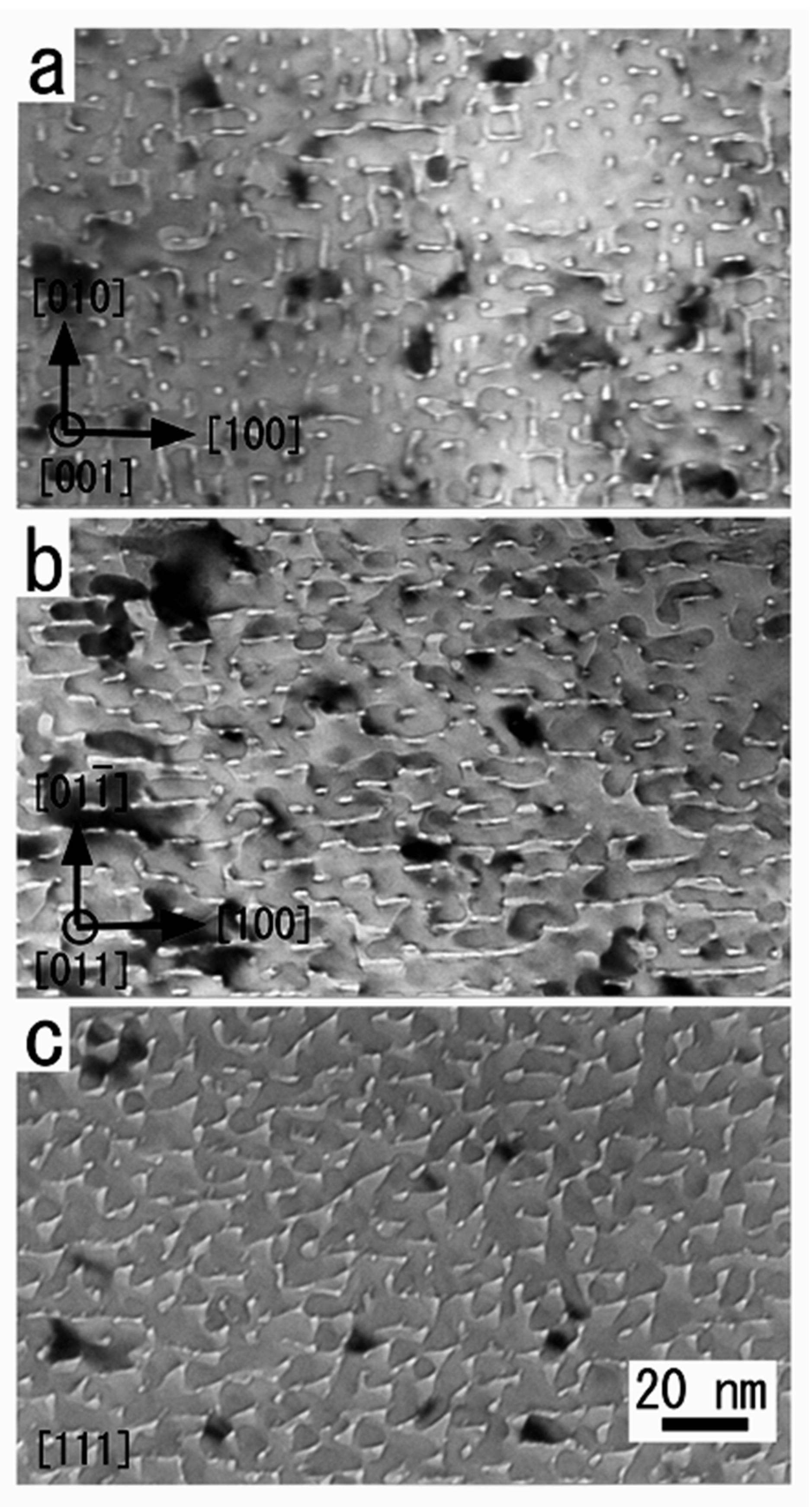
Figure 11 compares nanostructure, which appeared for Au(001), Ag(001), and Cu(001) foils irradiated with 400 keV electrons along [001] at 95 K [21]. Elongated bright images correspond to grooves formed on the electron exit surface of the foils. One can see that the patterns of grooves for both Ag and Cu are not as clear as the one for Au and extend weakly along [110] and [10] directions. The width of grooves for Cu is about 2–4 nm, significantly larger than those for Au and Ag, which are about 1–2 nm.
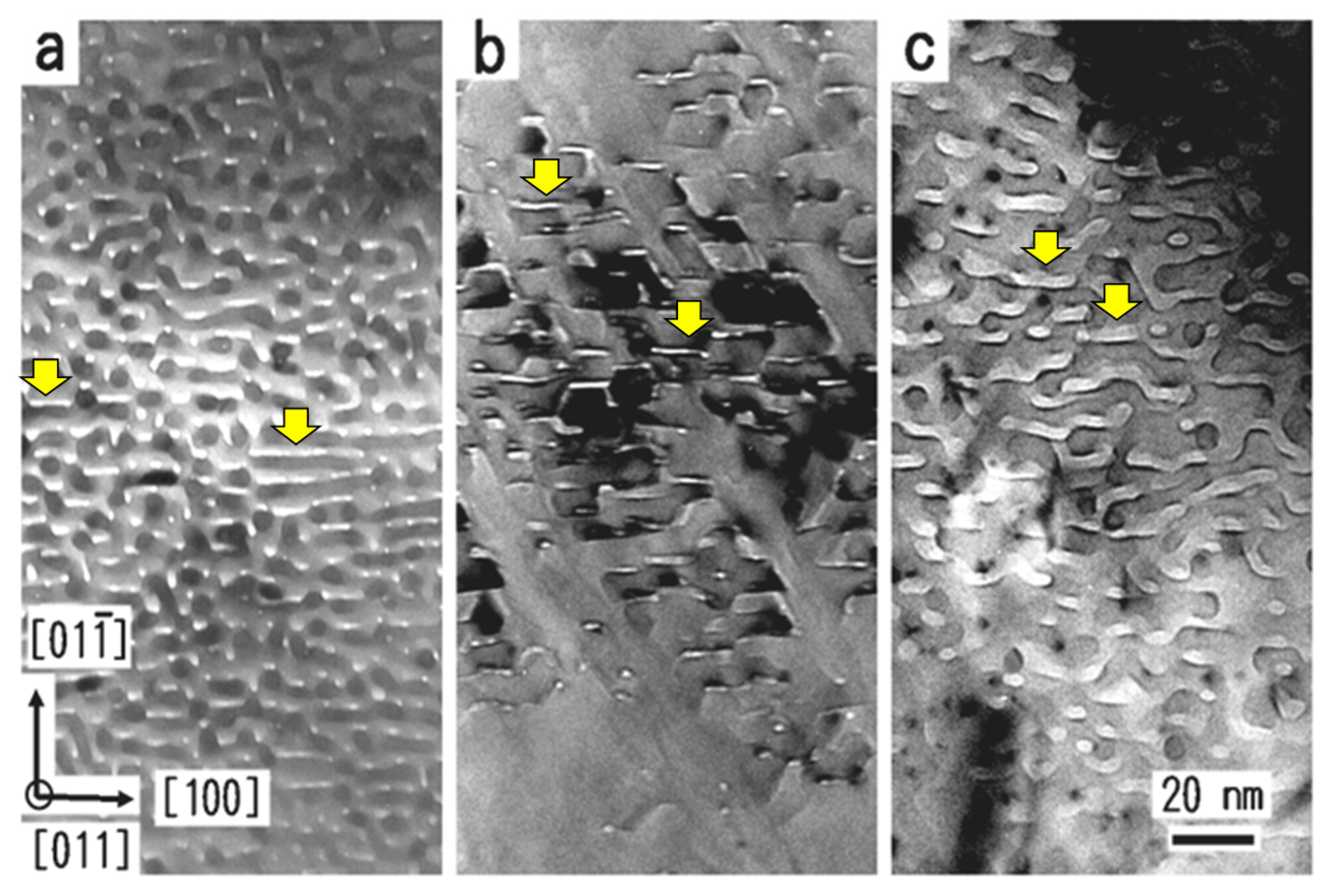
Contrary to the differences in the patterns for [001] irradiation, the groove formed by the oblique irradiations along [011] direction for Au, Ag, and Cu show a preferential elongation along [100], as denoted by arrows in Figure 12a–c. Note that the Ag specimen has a wavy surface. Then, the grooves formed on the surface are uneven and denuded in some areas, similar to the case of an Au foil with grain boundaries [11] but tend to grow along [100] in spite of the wavy surface. In addition to nanogrooves developed parallel to the exit surface of foils, nanoholes and hillocks are formed, as seen for Au, Ag, and Cu foils in Figure 13a–c, respectively [21]. The irradiations were done with 400 keV electrons at 95 K, and the photos were taken obliquely against the beam direction. Elongated images denoted by arrows correspond to nanoholes growing from the exit surface and dark contrasts denoted by h are hillocks. The directions of the growth of nanoholes and hillocks are along and opposite to the irradiation direction, respectively. One should note that the nanoholes grow deeper than 10 nm with an almost constant diameter of about 1–2 nm for Au and Ag and about 2–4 nm for Cu. Most of the nanoholes are formed in the areas of nanogrooves. The images of nanoholes observed along the irradiation direction can be found as extremely bright spots in Figure 12.
3.3. Ni
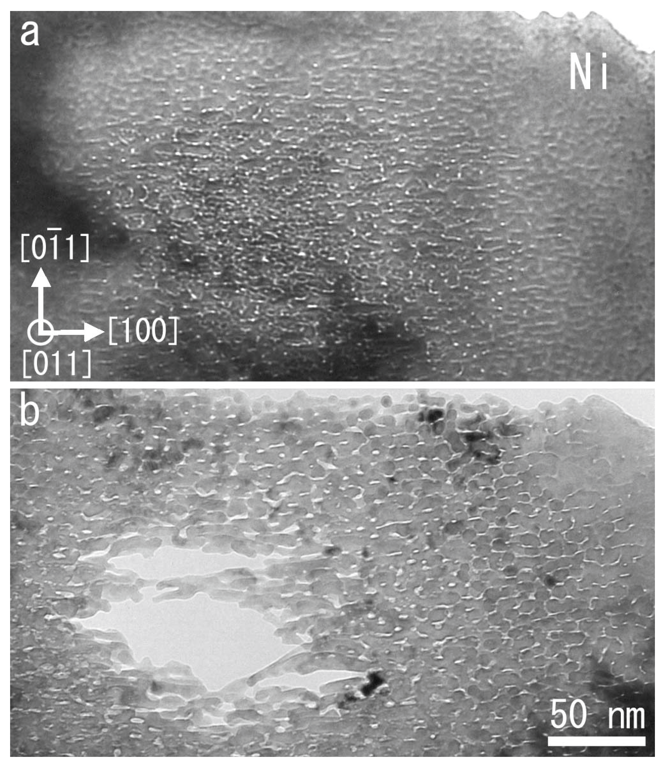
A nanostructure, which appeared for a Ni(001) foil irradiated with 400 keV electrons along [001] direction at 105 K to a dose of 7.0 × 1027 electrons m−2 [22], is shown in Figure 14. The diameter of electron beam for the irradiation was about 200 nm of which the center is near the center of Figure 14a. The micrograph was taken under a kinematic and slightly under-focus condition. One can see that the pattern near the center of the electron beam of photo (c) is rather different from that in the outer area of photo (c). The extension of bright images is not observed along [100] and [010] directions, but they extend slightly along [110] and [10] instead. The pattern near the center of the electron beam is similar to those of Ag and Cu, which are, respectively, shown in Figure 11b,c. The results for Ni mentioned above are different from those of Au, where the pattern is almost the same in the whole area, although the extension of the grooves becomes longer near the beam center, as seen in Figure 2.
Figure 15 shows the Ni(001) specimen, which was tilted to the direction near [011] and irradiated obliquely with 400 keV electrons along [011] direction at 105 K to a dose of 8.4 × 1027 electrons m−2. Bright images of nanogrooves tend to extend along [100], as shown in Figure 15a, similar to the cases of Au, Ag, and Cu (Figure 12). The irradiation was prolonged to a dose of 4.2 × 1028 electrons m−2, then the penetration of nanogrooves from the electron exit surface to the incident surface occurred, as seen in Figure 15b. We can find large holes appear near the center of an electron beam, and several nanowires were generated. The nanowires tend to elongate along [100], reflecting the initial pattern of nanogrooves seen in Figure 15a.
3.4. Iron
A nanostructure formed for a Fe(111) foil irradiated with 400 keV electrons along [111] direction at 300 K to a dose of 4.4 × 1028 electrons m−2 [22] is shown in Figure 16. The TEM micrograph was taken under a kinematic and slightly under-focus condition. The beam center is near the edge of the specimen. The nanostructure generated by the electron irradiation can be roughly divided into two types; one is high density of nanoholes formed in the outer area of the electron beam, as seen in the magnified view, and the other is nanogrooves, which are observed near the beam center.
The appearance of the two types of structure should be due to the difference in the total dose, as the beam intensity is stronger near the beam center. The irradiation dose described above is an average value. In situ observation has revealed that nanoholes are generated at first and then developed to nanogrooves with increasing dose. The diameter of nanoholes is about 2–4 nm. Formation of high density of nanoholes under electron irradiation has not been observed for Au, Ag, and Cu [21] but has been reported for Si [27].
One should note that a nanostructure with several nanometer size appeared at 300 K in the case of Fe. In the case of Au, on the other hand, the nanostructure appeared at 110 K and became unstable on annealing at room temperature. Nanoholes are transformed into voids with larger diameters, while the hillocks decreased in height, as shown in Figure 8. Then, the stepwise annealing was carried out with 50 K/10 min steps from 373 to 823 K in the transmission electron microscope to know the thermal stability of the nanostructure generated for Fe.
The changes on annealing at 623 and 823 K are, respectively, shown in Figure 17a,b. The pattern formed on the Fe surface scarcely changed up to 573 K, but a clear change can be observed above 623 K. The steps denoted by arrows are seen to move downwards. In spite of such an apparent change in the specimen surface on annealing at 623 K (Figure 17a), we can still observe some nanogrooves and nanoholes whose size and pattern are similar to those before annealing (Figure 16). At 823 K, on the other hand, a remarkable change such as disappearance of the nanostructures can be observed (Figure 17b). However, there still remains some nanoholes whose diameters are almost the same as those before annealing. The result is clearly different from that of Au, where nanoholes were transformed into voids with larger diameters, and the surface became smoother. The changes in the Au specimen suggest the remarkable effect of surface diffusion. Therefore, we guess that thermal evaporation of Fe atoms from the surface becomes remarkable at a temperature above 623 K to form the steps and to change the structure. Moreover, material transport on Fe surface by surface diffusion is not so significant as to change the nanostructure below 823 K.
However, residual O2 gas in the conventional TEM may affect the formation or the behavior of nanostructure similarly to the case of silicon [27]. Nonetheless, the electron exit surface of Fe where the pattern developed should be rather clean due to sputtering. Further investigations on this point are desired.
4. Discussion
For the generation of aligned nanogrooves, we did not use a convergent nanosized electron beam as has been done for the generation of nanoholes [10] but a homogeneous electron beam of about 200–800 nm in diameter. In this case, the phenomena occurring on the electron exit surface may be as follows (Figure 18). Surface vacancies are formed at first in the first layer of the metal. Then, the surface vacancies agglomerate to produce monolayer islands of surface vacancies. Under prolonged irradiation, surface vacancies are produced in the area of islands, and multilayered pits are formed in several minutes. One cannot expect any anisotropic movement of surface vacancies on (001) and (111) surfaces in the process, but it may be expected on (011), judging from the nature of geometrical symmetry of the surfaces. Therefore, the present results on the pattern formation on the (001) surface strongly suggest that we are dealing with a case of self-organized pattern formation controlled by some factor, which includes the anisotropy of material transfer.
We have found the formation of pits and the self-organization of grooves under electron irradiation. The growth process of the pits has been discussed theoretically by Cherns [11]. However, his model does not predict the generation of the deep nanoholes and the aligned nanogrooves found in the present work; probably, he used Au(111) foils on which the aligned nanogrooves do not appear. It is not clear when and why the aligned nanogrooves and the deep nanoholes are generated. In this section, we discuss the formation of deep nanoholes and the self-organization process of nanogrooves.
4.1. Formation Process of Deep Nanoholes
Figure 18 schematically shows the structural change in the electron exit surface at the initial stage of irradiation. At first, surface vacancies are formed in the first layer of the metal by sputtering. Then, the surface vacancies agglomerate to produce monolayer islands of surface vacancies. Under continuous irradiation, surface vacancies are formed in the area of islands, and finally, multilayered pits are generated. The growth process of the pits has been theoretically given by Cherns [11]. Nonetheless, his model does not predict the formation of the aligned nanogrooves and the deep nanoholes found in the present work.
In contrast with what has been said above for the formation of nanogrooves, the deepening of the nanoholes is not believed to involve self-organization. As may be seen from Figure 3, the diameters of nanoholes do not vary significantly along their depth, indicating one-dimensional growth along the irradiation direction. We can estimate that more than 2000 atoms must be removed to produce a nanohole of 1.5 nm width and 20 nm depth. We guess that irradiation-induced diffusion of surface vacancies plays a significant role, although there may be other processes leading to the deepening of nanohole. Note that the nanoholes are generated on the rear surface, growing opposite to the irradiation direction. Irradiation-induced diffusion of surface vacancies on the side walls of the holes can result in a vacancy migration opposite to the irradiation direction, which is towards the bottom of the nanohole. Thus, nanoholes can be deeper by this process.
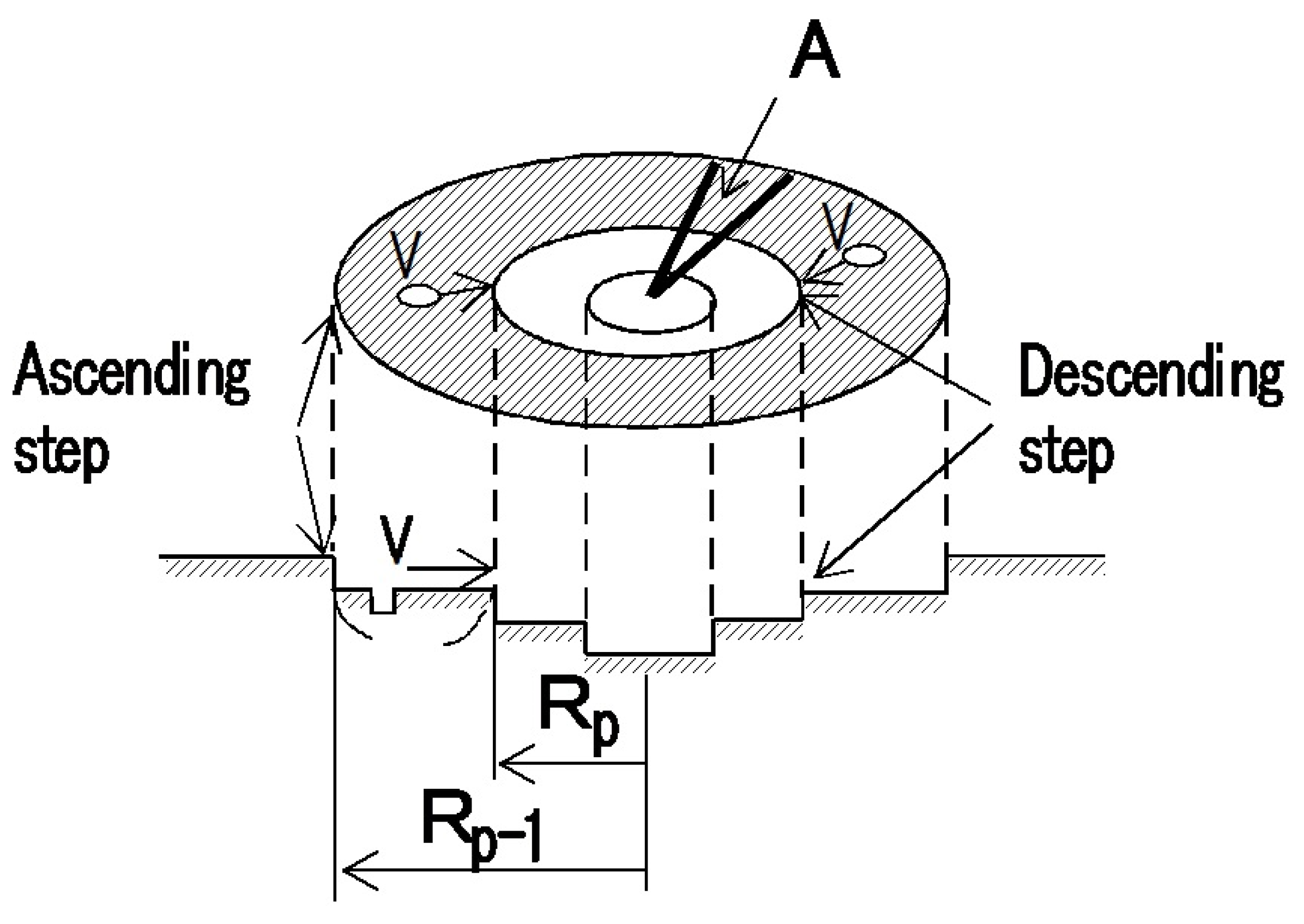
How does the nanohole grow so deep? First, one can consider that a geometrical factor would be responsible for the deepening of pits. Surface vacancies created in a terrace with a width w, as shown in Figure 19, can contribute to the erosion of the descending step but not of the ascending step at temperatures below which the layer-by-layer removal starts [28]. We can easily see that the area A in the terrace becomes larger near the center if the length of the descending step and the width of the terrace w are the same. This means that the erosion rate of the descending step near the center should be faster in this case due to the large amount of incoming surface vacancies for the unit length of the descending step. Under prolonged irradiation, however, the pit profile should reach a steady state after a critical dose, because a faster erosion of the descending step would lead to a decrease in the terrace width, thereby leading to a decrease in the erosion rate of the descending step.
Here, we discuss the pit profile in the steady state. The growth rate of the circular step with an inner radius of Rp in Figure 19 is given [11] in the continuum approximation by
where P and N0 are the production rate of surface vacancies and the number of atoms per unit area of the surface, respectively, and a0 is the atomic size.
dRp/dt = P(Rp−12 − Rp2)/2N0Rp (Rp > a0),
As Rp−1 = Rp + w, Equation (1) can be expressed as
dRp/dt = P[(Rp + w)2 − Rp2]/2N0Rp
= Pw/N0 + Pw2/2N0Rp,
= Pw/N0 + Pw2/2N0Rp,
When a pit grows steadily, Equation (2) should be constant (=k).
In the case where the terrace is far from the center (Rp > > w), the second term of Equation (2) is negligibly small. Then, the width of the terrace is approximately
w = kN0/P,
In the case where the terrace is located beside the center (Rp = w), the width of the terrace is estimated, by applying Rp = w and dRp/dt = k, as
w = (2/3)kN0/P,
The difference in the values of w in Equations (3) and (4) means that the width of the terrace near the center becomes narrower; i.e., the inclination of the face of the pit near the center becomes steeper. The shape of the steadily growing pit can be obtained by the numerical calculation for pit growth for finite intervals given by Cherns [11]. However, the result of these calculation does not reveal the significant deepening of pits observed in the present experimental study. Therefore, the deepening of the nanoholes should be due to some factors other than the geometrical factor.
Two factors can be mentioned as being responsible for the deepening, which are preferential sputtering at growth point and irradiation-induced diffusion. The sputtered surface quickly develops a high proportion of surface ledge sites, especially near the pit center, as seen in Figure 20. The sputtering rate would increase at the ledge sites due to the lower number of bonding. Therefore, it is probable that the preferential sputtering at the growth point leads to the deepening of pits. Irradiation-induced diffusion of surface vacancies and adatoms on the side walls of nanoholes, on the other hand, may play an important role. Surface vacancies and adatoms will move opposite to and along the irradiation direction, respectively, both movements enhancing the deepening of the holes.
4.2. Self-Organization of Nanogrooves
Interesting discovery on the development of nanostructure under electron irradiation in the present study is the pattern formation of nano-grooves, which can change depending on the irradiation directions, the irradiation temperatures, and the kinds of metals. The most outstanding feature appears for Au. The nanogrooves exhibit strong irradiation-direction dependencies in their growth. They grow along [100] and [010] directions for [001] irradiation and along [100] for [011] irradiation, whereas no clear grooves are formed for [111] irradiation. The widths of nanogrooves and holes are between about 1 and 2 nm, which are the smallest ones formed on metal surfaces so far. The formation of the groove pattern also has a surface orientation dependence.
To clarify the formation mechanism on the nanostructures, systematic investigations are needed. After finding the pattern formation for Au, we investigated several FCC metals of Au, Ag, Cu, Ni, and a BCC metal of Fe. For Ag and Cu, the pattern formation is not so clear. For Ni, the diffusion effect is not so high compared to the cases of Ag and Cu, but the pattern depended on the part of the specimen, as seen in Figure 11. For Fe, the pattern is not clear but rather random (Figure 14).
The generation of nanoholes and nanogrooves originally comes from the sputtering at the electron exit surface. Thus, the anisotropic growth of the nanogrooves and nanoholes should be attributed to the irradiation-induced anisotropic flow of point defects [29].
The fact that different groove patterns observed on the same Au(001) surface by irradiating along different directions (Figure 4 and Figure 5) strongly suggests that the patterns are meta-stable structures, which has a very long lifetime at low temperatures.
The available experimental evidence demonstrates that we are dealing with a case of self-organized pattern formation, which satisfies the following conditions.
- (1)
- The groove patterns are generated far from thermal equilibrium in an open, highly dissipative system.
- (2)
- Only a small fraction of the total energy input is stored (e.g., as surface energy at the grooves).
Below 240 K, the temperature effect of surface vacancy, which will reduce the anisotropic growth of nanogrooves due to their random movements, should be low for Au, as seen in Figure 10. At the low temperature region, the migration of surface vacancies by thermal activation alone should be negligibly small. Thus, we may expect the phenomena observed to be controlled by some anisotropic mechanisms such as sputtering induced by the anisotropy of the sputtering yield [23], the surface reconstruction under irradiation [25], focused collision chains [30], or irradiation-induced diffusion [29].
We guess that the anisotropy of momentum transfer, either directly from the electrons by Rutherford scattering or indirectly through bulk collision sequences propagating along the densely packed directions, leads to the mobility of surface vacancies, finally leading to anisotropic groove patterns. One should note that there exists a difference in the anisotropy of collision sequence propagation between bulk Au and Ag, i.e., along the <100> direction for Au but <110> for Ag, which was experimentally supported by a difference in the anisotropy of the threshold energy for atom displacement in both materials [30].
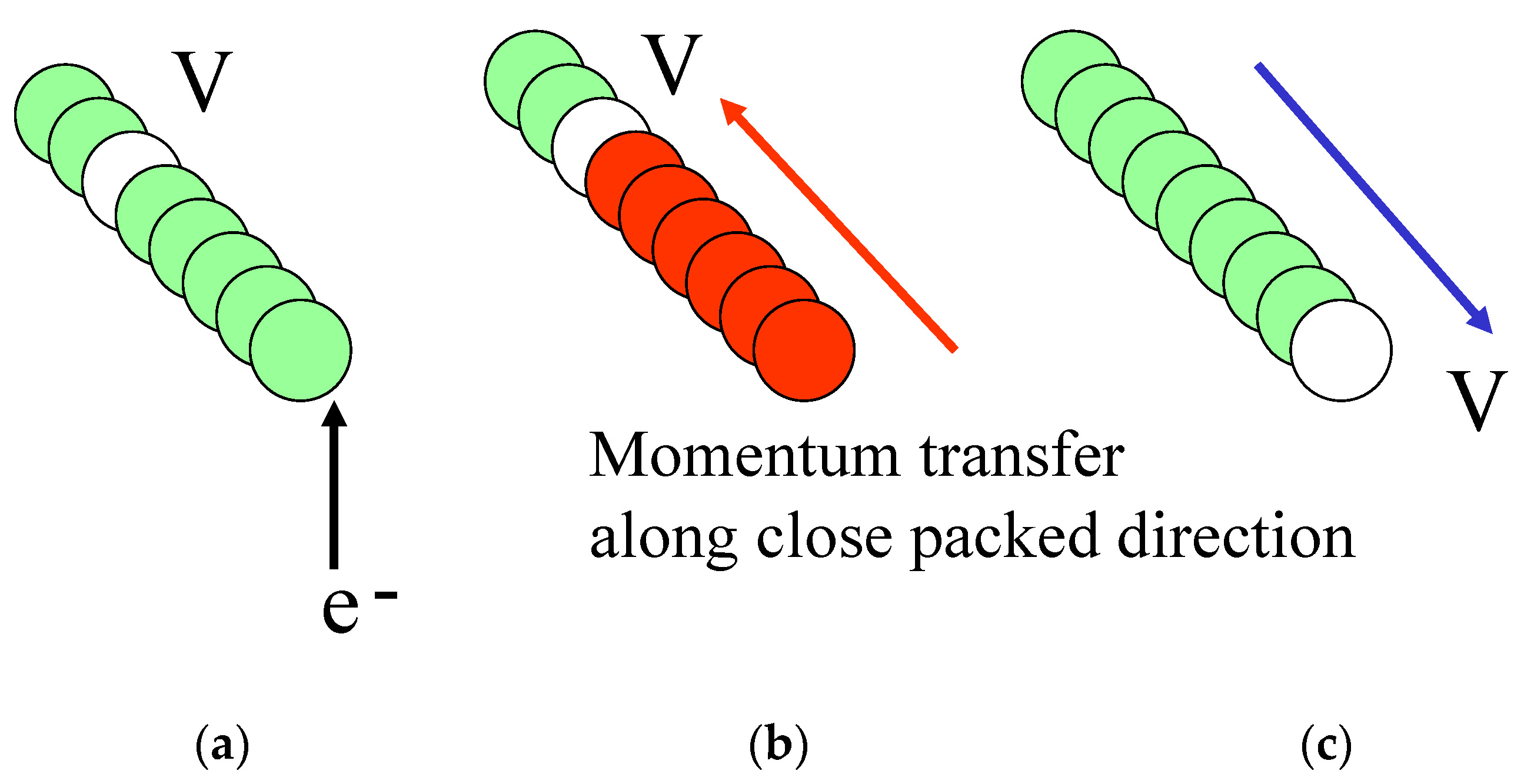
Now, we draw a conceivable scenario, in the following section. Consider a surface atom of which momentum has been transferred either directly from the electrons by Rutherford scattering or indirectly through bulk collision sequences. In the case where the component of the transferred momentum normal to the surface is sufficiently large, the atom will be sputtered off the surface leaving a surface vacancy behind. Surface collision sequences propagating along close-packed directions in the surface shown in Figure 21 may be excited by momentum transfer to neighboring atoms—a process that is favored by the angular dependence of the Rutherford scattering cross-section. Under prolonged irradiation, the surface vacancies will move around by irradiation-induced diffusion and may agglomerate to form pits. Surface collision sequences ending at a descending surface step or at a hole or groove, on the other hand, may generate a surface adatom, leaving a surface vacancy at or near its point of departure. Adatoms created on the surfaces of grooves will in general reduce the groove surface area. Since the propagation of collision sequences is highly anisotropic, this may lead to a gradual alignment of the grooves and pits under prolonged irradiation. This process is similar to that of the formation of lattices of stacking-fault tetrahedra under high-dose electron irradiation [12,13]. Such a mechanism can work only if the mobility of the surface vacancies is not too large. This probably accounts for the fact that regular groove patterns have so far been observed for Au only after low-temperature irradiation but not under room-temperature irradiation conditions.
Additionally, one should note that the pattern of aligned nanogroove for the 400 keV electron irradiation for Au (Figure 2) is clearer than the one for the 800 keV electron irradiation (Figure 4). The origin of the less clear pattern in the latter case should be attributed to some additional effects such as a complicated sputtering process; that is, at energies <600 keV, surface atoms are sputtered by direct recoils only, whereas at energies >600 keV, up to about 10% of the total yield comprises surface atoms sputtered by sub-surface recoils [23] and the formation of Frenkel pairs, which can occur at higher irradiation energy of electrons [24]. Angular distributions of sputtered atoms as a function of electron energy [23] may affect the formation of adatoms and the pattern formation. Moreover, the formation of aligned nanogrooves and nanoholes are significantly affected by the irradiation temperature (Figure 9 and Figure 10), probably reflecting the mobility of surface vacancy.
5. Conclusions
We found a new type of self-organized nanostructure formation on the exit surface of thin gold foils irradiated with high doses of 360–1250 keV electrons at temperatures of about 100 K. The structure consists of aligned nanogrooves, which develop parallel to the surface, and nanoholes and hillocks, which grow parallel to the electron beam. The nanogrooves show strong irradiation-direction dependencies on their growth. They grow along [100] and [010] directions for [001] irradiation, along [100] for the [011] irradiation, whereas no clear grooves are formed for [111] irradiation. The widths of nanogrooves and holes are between about 1 and 2 nm, which are the smallest ones generated on metal surfaces so far. The final structures of the thin foils under electron irradiation are nanoparticles or nanowires. This method has been utilized to produce long gold nanowires for investigations of the interesting physics such as the electron transport properties and the multi-shell structure. Temperature dependence of the nanostructure for gold indicates that the effect of surface diffusion becomes significant above 240 K.
Furthermore, the self-organized structures for silver, copper, nickel, and iron are investigated. The formation of nanoholes and nanogrooves basically originates in the sputtering at the electron exit surface. The difference in the anisotropic growth of the nanogrooves and nanoholes among the kinds of metals should be attributed to the irradiation-induced anisotropic flow of point defects and some related factors, which are attributed to the nature of metals. Thus, we can use the present investigation for the studies of irradiation-induced effects and the surface diffusion effect, of which knowledge should be useful for the synthesis of new nanomaterials.
Funding
This study was supported by fellowships from the Ministry of Education of Japan and Max-Planck-Institut.
Acknowledgments
I express my sincere thanks to Wilfried Sigle, Fritz Phillipp, the late Alfred Seeger, and Hiroaki Abe for their collaboration. Experimental works were mostly done in Max-Planck-Institut für Metallforschung and partly Japan Atomic Energy Research Institute-Takasaki.
Conflicts of Interest
The authors declare no conflict of interest.
References
- Wua, T.; Lin, Y.-W. Surface-enhanced Raman scattering active gold nanoparticle/nanohole arrays fabricated through electron beam lithography. Appl. Surf. Sci. 2018, 435, 1143. [Google Scholar] [CrossRef]
- Tavakoli, M.; Jalili, Y.S.; Elahi, S.M. Rayleigh-Wood anomaly approximation with FDTD simulation of plasmonic gold nanohole array for determination of optimum extraordinary optical transmission characteristics. Superlattices Microstruct. 2019, 130, 454. [Google Scholar] [CrossRef]
- Chen, X.; Wang, H.; Xu, N.-S.; Chen, H.; Deng, S. Resonance coupling in hybrid gold nanohole–monolayer WS2 nanostructures. Appl. Mater. Today 2019, 15, 145. [Google Scholar] [CrossRef]
- Becker, R.S.; Golovchenko, J.A.; Swartzentruber, B.S. Atomic-scale surface modifications using a tunnelling microscope. Nature 1987, 325, 419. [Google Scholar] [CrossRef]
- Eiger, D.M.; Schweizer, E.K. Positioning single atoms with a scanning tunnelling microscope. Nature 1990, 344, 524. [Google Scholar] [CrossRef]
- Kobayashi, A.; Grey, F.; Williams, R.S.; Aono, M. Formation of nanometer-scale grooves in silicon with a scanning tunneling microscope. Science 1993, 259, 1724. [Google Scholar] [CrossRef] [PubMed]
- Saif, M.J.; Naveed, M.; Asif, H.M.; Akhtar, R. Irradiation applications for polymer nano-composites: A state-of-the-art review. J. Ind. Eng. Chem. 2018, 60, 218. [Google Scholar] [CrossRef]
- Córdoba, R.; Orús, P.; Strohauer, S.; Torres, T.E.; Teresa, J.M.D. Ultra-fast direct growth of metallic micro- and nano-structures by focused ion beam irradiation. Sci. Rep. 2019, 9, 14076. [Google Scholar] [CrossRef] [PubMed] [Green Version]
- Turner, P.S.; Bullogh, T.J.; Devenish, R.W.; Maher, D.M.; Humphereys, C.J. Nanometre hole formation in MgO using electron beams. Philos. Mag. Lett. 1990, 61, 181. [Google Scholar] [CrossRef]
- Kizuka, T.; Tanaka, N. Nanometre scale electron beam processing and in situ atomic observation of vacuum-deposited MgO films in high-resolution transmission electron microscopy. Philos. Mag. A 1995, 71, 631. [Google Scholar] [CrossRef]
- Cherns, D. The surface structure of (111) gold films sputtered in the high voltage electron microscope a theoretical model. Philos. Mag. 1977, 36, 1429. [Google Scholar] [CrossRef]
- Jin, N.Y.; Phillipp, F.; Seeger, A. Investigation of defect ordering in heavily irradiated metals by high-voltage electron microscopy. Phys. Stat. Sol. 1989, 116, 91. [Google Scholar] [CrossRef]
- Seeger, A.; Jin, N.Y.; Phillipp, F.; Zaiser, M. The study of self-organization processes in crystals by high-voltage electron microscopy. Ultramicroscopy 1991, 39, 342. [Google Scholar] [CrossRef]
- Ghoniem, N.M.; Walgraef, D.; Zinkle, S.J. Theory and experiment of nanostructure self-organization in irradiated materials. J. Comput. Aided Mater. Des. 2001, 8, 1. [Google Scholar] [CrossRef]
- Kharchenko, D.O.; Kharchenko, V.O.; Bashtova, A.I. Modeling self-organization of nano-size vacancy clusters in stochastic systems subjected to irradiation. Radiat. Eff. Defects Solids 2014, 169, 418. [Google Scholar] [CrossRef] [Green Version]
- Gao, Y.; Zhang, Y.; Schwen, D.; Jiang, C.; Sun, C.; Gan, J.; Bai, X.-M. Theoretical prediction and atomic kinetic Monte Carlo simulations of void superlattice self-organization under irradiation. Sci. Rep. 2018, 8, 6629. [Google Scholar] [CrossRef] [PubMed] [Green Version]
- Vitral, E.; Walgraef, D.; Pontes, J.; Anjos, G.R.; Mangiavacchi, N. Nano-patterning of surfaces by ion sputtering: Numerical study of the anisotropic damped Kuramoto-Sivashinsky equation. Comput. Mater. Sci. 2018, 146, 193. [Google Scholar] [CrossRef]
- Niwase, K.; Sigle, W.; Phillipp, F.; Seeger, A. Generation of nanosized grooves and holes on metal surfaces by low-temperature electron irradiation. Philos. Mag. Lett. 1996, 74, 167. [Google Scholar] [CrossRef]
- Niwase, K.; Sigle, W.; Phillipp, F.; Seeger, A. Nanogrooves generated on Au surfaces by low-temperature electron irradiation. J. Surf. Anal. 1997, 3, 440. [Google Scholar]
- Niwase, K.; Sigle, W.; Phillipp, F.; Seeger, A. Novel phenomena of irradiation damage in FCC metals irradiated with high-energy electrons at low temperatures. J. Electron. Microsc. 1999, 48, 495. [Google Scholar] [CrossRef]
- Niwase, K.; Phillipp, F.; Seeger, A. Self-organized nanostructures generated on Au, Ag and Cu surfaces by low-temperature electron irradiation. Jpn. J. Appl. Phys. 2000, 39, 4624. [Google Scholar] [CrossRef]
- Niwase, K.; Abe, H. Generation of nanosized structures on Ni and Fe surfaces by electron irradiation. Mater. Trans. 2002, 43, 646. [Google Scholar] [CrossRef] [Green Version]
- Cherns, D. Sputtering of gold foils in a high voltage electron microscope a comparison of theory and experiment. Philos. Mag. 1977, 35, 693. [Google Scholar] [CrossRef]
- Hohenstein, M.; Seeger, A.; Sigle, W. The anisotropy and temperature dependence of the threshold for radiation damage in gold—comparison with other FCC metals. J. Nucl. Mater. 1989, 169, 33. [Google Scholar] [CrossRef]
- Kondo, Y.; Takayanagi, K. Gold nanobridge stabilized by surface structure. Phys. Rev. Lett. 1997, 79, 3455. [Google Scholar] [CrossRef] [Green Version]
- Kondo, Y.; Takayanagi, K. Synthesis and characterization of helical multi-shell gold nanowires. Science 2000, 289, 606. [Google Scholar] [CrossRef] [PubMed]
- Takeda, S.; Koto, K.; Iijima, S.; Ichihashi, T. Nanoholes on silicon surface created by electron irradiation under ultrahigh vacuum environment. Phys. Rev. Lett. 1997, 20, 2994. [Google Scholar] [CrossRef]
- Michely, T.; Land, T.; Littmark, U.; Comsa, G. Morphological effects induced by the formation of a Pt-adatom lattice gas on Pt (111). Surf. Sci. 1992, 272, 204. [Google Scholar] [CrossRef]
- Urban, K.; Seeger, A. Radiation-induced diffusion of point-defects during low-temperature electron irradiation. Philos. Mag. 1974, 30, 1395. [Google Scholar] [CrossRef]
- Sigle, W. The anisotropy of the threshold energy for atom displacements in silver. J. Phys Condens. Matter. 1991, 3, 3921. [Google Scholar] [CrossRef]
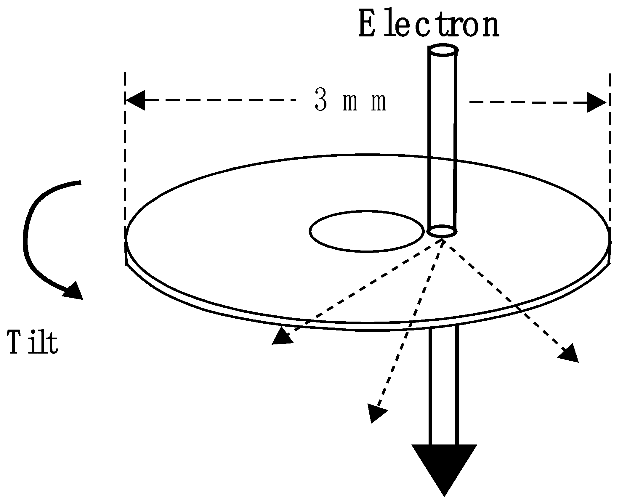
Figure 1.
A schematic view of a disk specimen of 3 mm diameter. The irradiations were carried out at thin parts near a hole with an electron beam of about 200–800 nm diameter.
Figure 1.
A schematic view of a disk specimen of 3 mm diameter. The irradiations were carried out at thin parts near a hole with an electron beam of about 200–800 nm diameter.

Figure 2.
(a) TEM micrographs of an Au(001) foil irradiated along [001] with 400 keV electrons at 95 K; (b) a magnified view of black square area in photo (a).
Figure 2.
(a) TEM micrographs of an Au(001) foil irradiated along [001] with 400 keV electrons at 95 K; (b) a magnified view of black square area in photo (a).

Figure 3.
Nanoholes and hillocks generated on the exit surface of an Au(001) foil, which was irradiated along [112] with 400 keV electrons at 95 K and observed along [001]. Nanoholes and hillocks are denoted by arrows and by h, respectively.
Figure 3.
Nanoholes and hillocks generated on the exit surface of an Au(001) foil, which was irradiated along [112] with 400 keV electrons at 95 K and observed along [001]. Nanoholes and hillocks are denoted by arrows and by h, respectively.

Figure 4.
TEM micrographs of an Au(00l) foil irradiated at 110 K with 800 keV electrons to a fluence of about 8 × 10⁶ electrons m−2. The directions of irradiations and observations are (a) [001], (b) [011], and (c) [111].
Figure 4.
TEM micrographs of an Au(00l) foil irradiated at 110 K with 800 keV electrons to a fluence of about 8 × 10⁶ electrons m−2. The directions of irradiations and observations are (a) [001], (b) [011], and (c) [111].

Figure 5.
Schematic views of the sputtered rear surface of Au(001) foils irradiated with 800 keV electrons along (a) the [001] direction, (b) the [011] direction, and (c) the [111] direction.
Figure 5.
Schematic views of the sputtered rear surface of Au(001) foils irradiated with 800 keV electrons along (a) the [001] direction, (b) the [011] direction, and (c) the [111] direction.

Figure 6.
Development of nanostructure on the exit surface of an Au(011) foil irradiated with 400 keV electrons along [011] direction at 95 K: (a) 300 s; (b) 480 s; (c) 600 s; (d) 750 s.
Figure 6.
Development of nanostructure on the exit surface of an Au(011) foil irradiated with 400 keV electrons along [011] direction at 95 K: (a) 300 s; (b) 480 s; (c) 600 s; (d) 750 s.
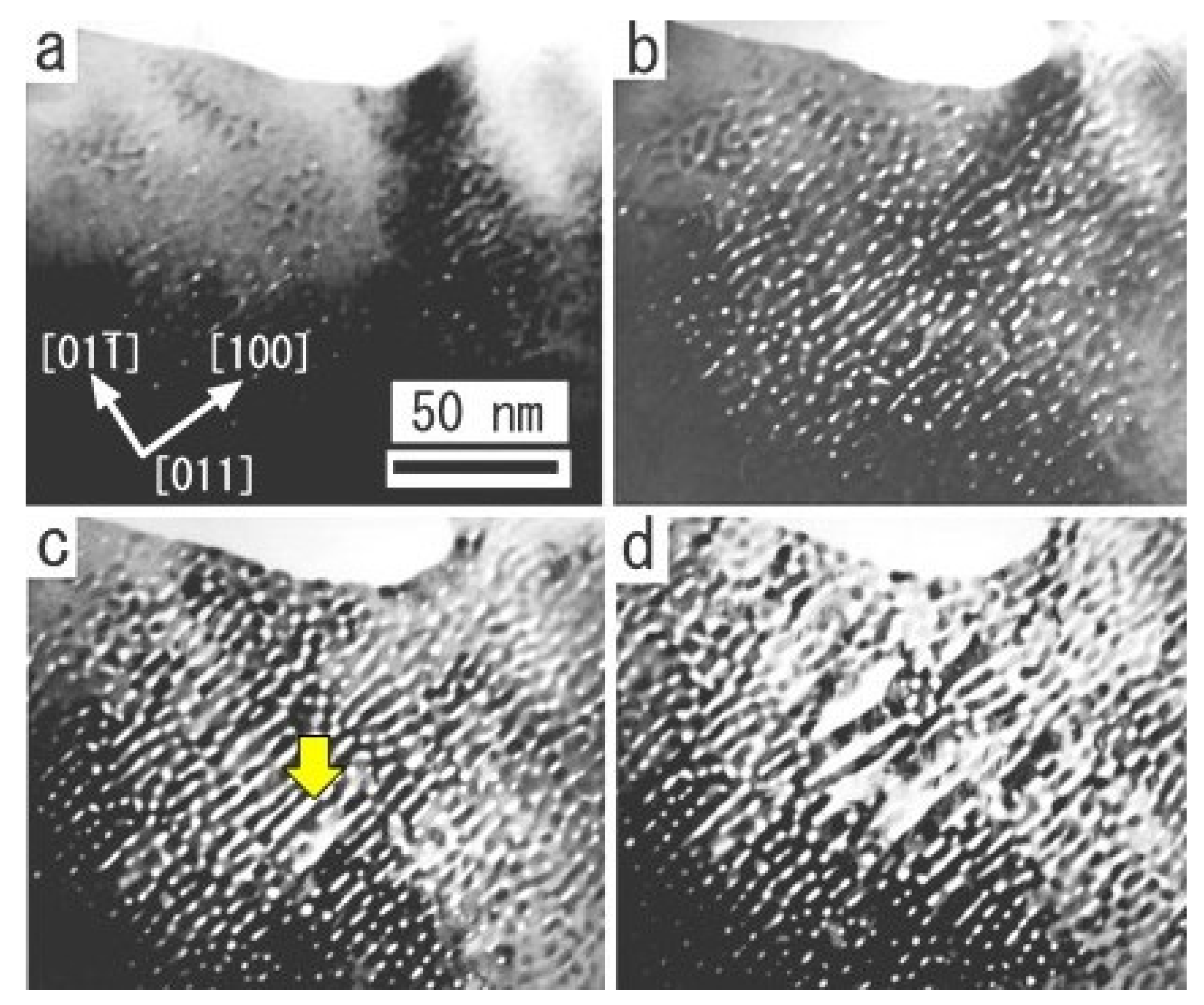
Figure 7.
Nanostructures of Au(001) foils irradiated with 1.25 MeV electrons at 110 K along: (a) [001] direction, 1500 s; (b) [111] direction, 1700 s. The structures near the beam center are seen to be nanoparticles connected to each other and depend on the irradiation direction.
Figure 7.
Nanostructures of Au(001) foils irradiated with 1.25 MeV electrons at 110 K along: (a) [001] direction, 1500 s; (b) [111] direction, 1700 s. The structures near the beam center are seen to be nanoparticles connected to each other and depend on the irradiation direction.

Figure 8.
TEM micrographs of an area of Au foil (a) irradiated along [111] direction at 800 keV with a fluence of about 8 × 1026 electrons m−2 then (b) annealed at room temperature. Both the photos were taken along [001] direction. The projection of the electron-beam direction during irradiation is shown by a yellow arrow in photo (a). Voids transformed from nanoholes are indicated by arrows in photo (b).

Figure 9.
Au(001) foils irradiated along the [001] direction with 1250 keV electrons. (a) 110 K, 1070 s; (b) 240 K, 2130 s; (c) 270 K, 1180 s; (d) 300 K, 2680 s.
Figure 9.
Au(001) foils irradiated along the [001] direction with 1250 keV electrons. (a) 110 K, 1070 s; (b) 240 K, 2130 s; (c) 270 K, 1180 s; (d) 300 K, 2680 s.

Figure 10.
Arrhenius plot of the density of nanoholes. Two linear relations are seen, giving apparent activation energies of 0.0046 eV below 240 K and 0.088 eV above 240 K.
Figure 10.
Arrhenius plot of the density of nanoholes. Two linear relations are seen, giving apparent activation energies of 0.0046 eV below 240 K and 0.088 eV above 240 K.

Figure 11.
Nanostructures generated on (a) Au(001), (b) Ag(001), and (c) Cu(001) foils under 400 keV electron irradiation along [001] direction at 95 K. The patterns of grooves for both Ag and Cu are not as clear as the one for Au. The width of grooves for Cu is about 2–4 nm, significantly larger than those for Au and Ag, which are about 1–2 nm.

Figure 12.
TEM images of nanostructure generated on the exit surface of Au, Ag, and Cu foils irradiated with 400 keV electrons along [011] direction at 95 K: (a) Au(001), 600 s; (b) Ag(001), 510 s; (c) Cu(001), 2160 s. Nanogrooves with bright contrast are seen to elongate along [100] direction for all the cases.

Figure 13.
TEM images of deep nanoholes and hillocks generated on the exit surface of Au, Ag, and Cu foils irradiated with 400 keV electrons at 95 K: (a) Au(001), 600 s; (b) Ag(001) 600 s; (c) Cu(001), 3180 s. All images were taken oblique to the irradiation directions. Nanoholes and hillocks denoted by arrows and by h are seen to elongate opposite to and along the beam direction, respectively.

Figure 14.
(a) TEM micrograph of nanostructures generated on the exit surface of Ni(001) foil irradiated with 400 keV electrons along [001] direction at 105 K to a dose of 7.0 × 1027 electrons m−2. (b) A magnified view of the outer area of the electron beam. (c) A magnified view of the area near the beam center.
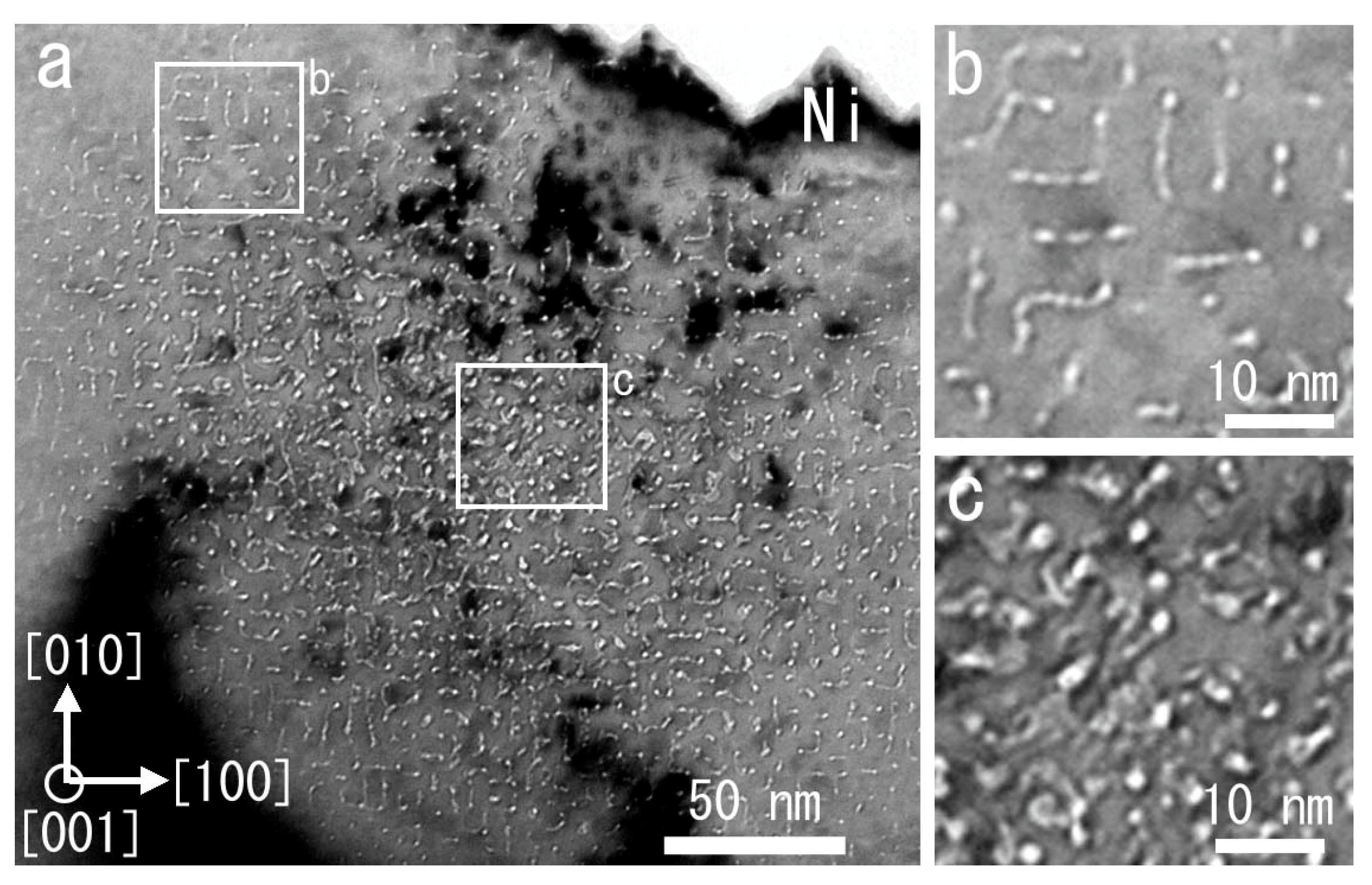
Figure 15.
TEM micrographs of Ni(001) specimen tilted to the direction near [011] direction. Irradiation was done with 400 keV electrons along [011] direction at 105 K to doses of (a) 8.4 × 1027 e−m−2 and (b) 4.2 × 1028 e−m−2. Penetration of the foil can be seen in photo (b).
Figure 15.
TEM micrographs of Ni(001) specimen tilted to the direction near [011] direction. Irradiation was done with 400 keV electrons along [011] direction at 105 K to doses of (a) 8.4 × 1027 e−m−2 and (b) 4.2 × 1028 e−m−2. Penetration of the foil can be seen in photo (b).

Figure 16.
TEM micrographs of the Fe(111) foil irradiated with 400 keV electrons along [011] direction at 300 K to a dose of 4.4 × 1028 electrons m−2. A magnified view of the nanoholes is given in the inset.
Figure 16.
TEM micrographs of the Fe(111) foil irradiated with 400 keV electrons along [011] direction at 300 K to a dose of 4.4 × 1028 electrons m−2. A magnified view of the nanoholes is given in the inset.

Figure 17.
The change in nanostructure of the Fe(111) foil on annealing at (a) 623 K and (b) 823 K. The nanostructure was generated by the irradiation with 400 keV electrons along the [011] direction at 300 K to a fluence of 4.4 × 1028 electrons m−2. Steps that appeared on annealing are denoted by arrows in photos (a,b).
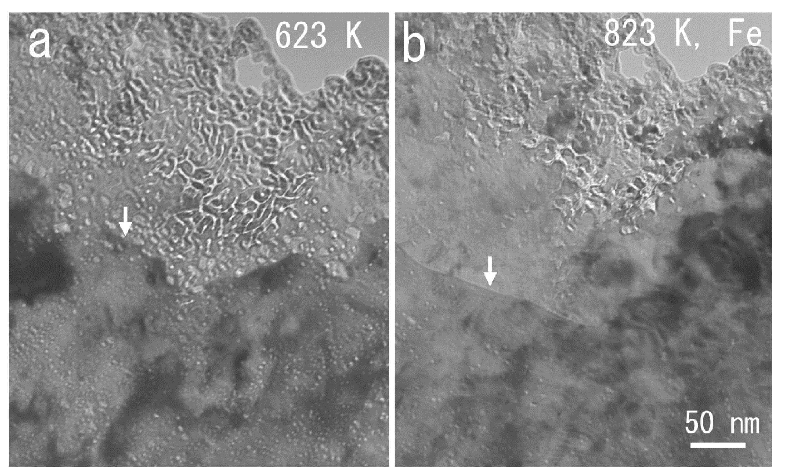
Figure 18.
A sketch of the change in the electron exit surface at the initial stage of formation of pits. 1. At first, vacancies are formed on the surface layer of the foil by sputtering. 2. They then agglomerate to form monolayer islands of surface vacancies. 3. After prolonged irradiation, further surface vacancies are formed within islands. 4. Finally, multilayered pits will be formed.
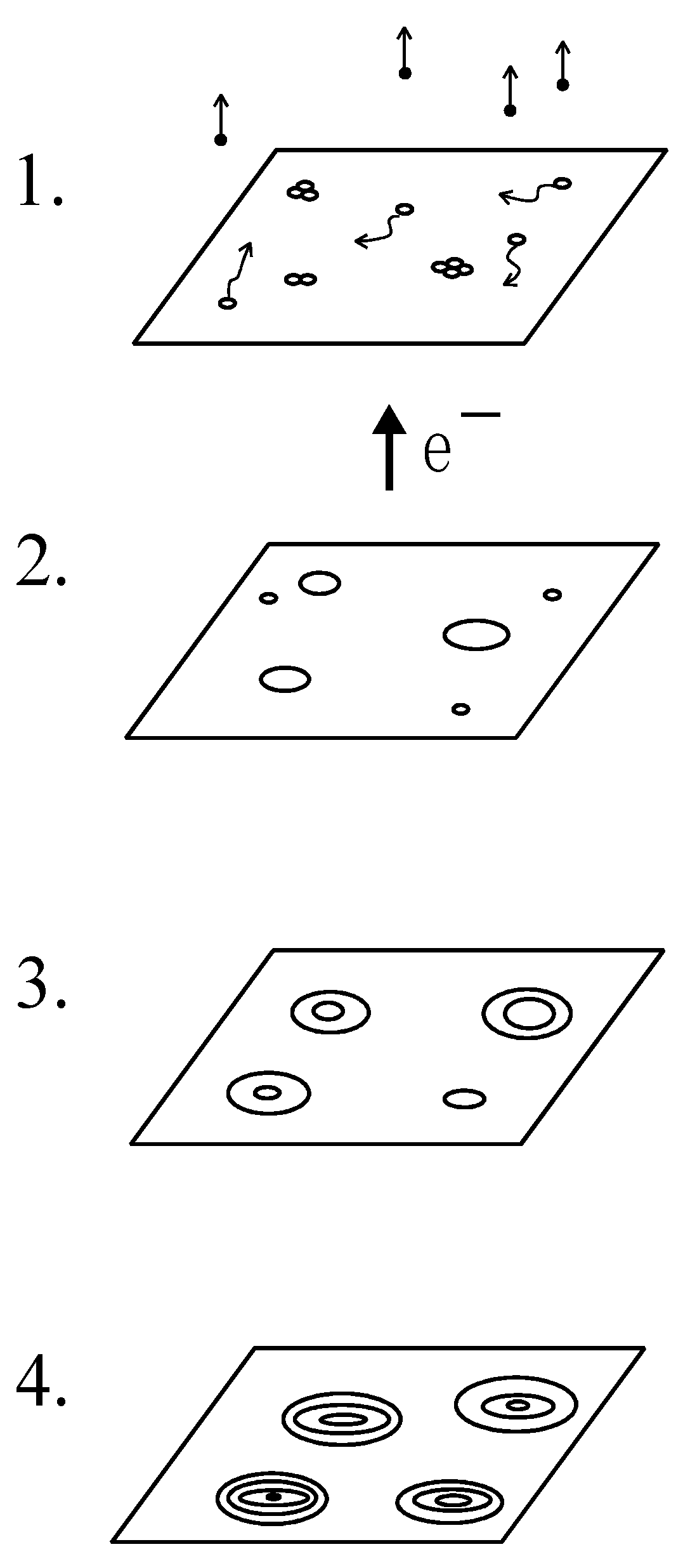
Figure 19.
Oblique and cross-sectional views of a circular pit. Surface vacancies created in a terrace with width w can contribute to the erosion of the descending step but not of the ascending step at temperatures below that at which the layer-by-layer removal starts [28].
Figure 19.
Oblique and cross-sectional views of a circular pit. Surface vacancies created in a terrace with width w can contribute to the erosion of the descending step but not of the ascending step at temperatures below that at which the layer-by-layer removal starts [28].

Figure 20.
Growth process of nanohole. Surface vacancies on the wall of nanohole move to the tip of nanohole, but adatoms are evacuated from the nanohole. Thus, deep nanoholes can be formed.
Figure 20.
Growth process of nanohole. Surface vacancies on the wall of nanohole move to the tip of nanohole, but adatoms are evacuated from the nanohole. Thus, deep nanoholes can be formed.
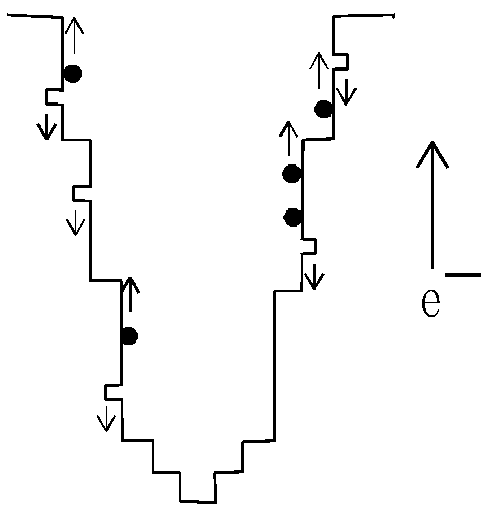
Figure 21.
Movement of vacancy due to momentum transfer along close-packed direction. White circle indicates surface vacancy. (a) Collision of electron, (b) momentum transfer along close packed direction given by the collision of electron, (c) movement of surface vacancy opposite to the direction of momentum transfer along close packed direction.
Publisher’s Note: MDPI stays neutral with regard to jurisdictional claims in published maps and institutional affiliations. |
© 2021 by the author. Licensee MDPI, Basel, Switzerland. This article is an open access article distributed under the terms and conditions of the Creative Commons Attribution (CC BY) license (http://creativecommons.org/licenses/by/4.0/).
Share and Cite
MDPI and ACS Style
Niwase, K. Self-Organized Nanostructures Generated on Metal Surfaces under Electron Irradiation. Quantum Beam Sci. 2021, 5, 4. https://0-doi-org.brum.beds.ac.uk/10.3390/qubs5010004
AMA Style
Niwase K. Self-Organized Nanostructures Generated on Metal Surfaces under Electron Irradiation. Quantum Beam Science. 2021; 5(1):4. https://0-doi-org.brum.beds.ac.uk/10.3390/qubs5010004
Chicago/Turabian StyleNiwase, Keisuke. 2021. "Self-Organized Nanostructures Generated on Metal Surfaces under Electron Irradiation" Quantum Beam Science 5, no. 1: 4. https://0-doi-org.brum.beds.ac.uk/10.3390/qubs5010004