1. Introduction
For material nanofabrication using an electron beam, a sample is irradiated with a high-intensity electron beam using a field-emission electron gun. The development of a pulsed electron source with high emittance in a short time is effectively used not only for material nanofabrication but also for high-speed observation of electron irradiation-induced material behavior and observation with reduced electron irradiation effect of polymers when used for TEM. For example, the dislocation motion is in the scale from 1 s to 1 ms, the nucleation and growth in the scale from 1 ms to 0.1 ps, and the magnetic switching or melting and solidification in the scale from 10 ns to 0.1 ps. The time scale on which physical phenomena, such as phase transitions, occur is in the scale from 1 ns to 10 fs [
1].
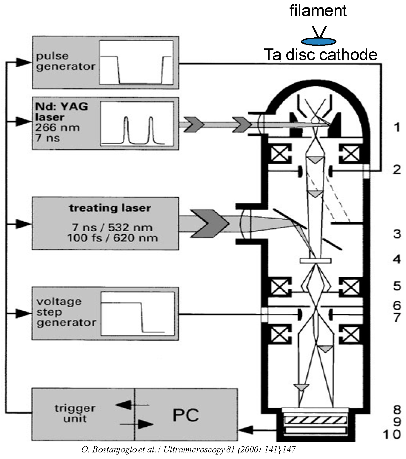
The development of a TEM equipped with a laser photocathode electron gun has been in progress since around 2000. As shown in
Figure 1, the first machine was manufactured at the Berlin Institute of Technology. Using the pulsed electrons emitted from a Ta cathode excited by an Nd:YAG laser (wavelength, 266 nm; pulse width, 7 ns; current density, 700 A/cm
2; brightness, ~4 × 10
6 A/cm
2 str), a spatial resolution of ~100 nm and a temporal resolution of ~1 ns were achieved by the pulsed electrons [
2]. After that, in 2007, at Lawrence Livermore National Laboratory in the United States, a spatial resolution of ~10 nm and a temporal resolution of ~1 ns were achieved [
3]. In 2008, at the California Institute of Technology in the United States, the temporal resolution was improved to ~10 ps in the same spatial resolution of ~10 nm [
4]. Recently in 2016, at CNRS National Laboratory in France, an atomic resolution of ~0.2 nm and a temporal resolution of ~370 fs were successfully achieved [
5].
In the developments mentioned above, the cathode material is a metal, but by replacing it with compound semiconductors, it is possible to further increase the emittance. Using III–V compound semiconductor substrates, such as GaAs, with a negative electron affinity (NEA) surface is useful to generate pulsed electrons with small energy dispersion with high emittance. However, it is difficult to handle because the usable vacuum environment is severe, and an extremely high vacuum is required to extend the lifetime [
6,
7,
8,
9,
10,
11].
The advantage of using the NEA semiconductor surface is it reduces the work function. The role of Cs in NEA surface preparation has not been clarified in detail. The NEA treatment method involves forming a dipole layer of Cs with a positive charge on the semiconductor surface by repeating Cs vapor deposition and oxygen adsorption at a substrate temperature of about 550 °C. This dipole layer is thought to reduce the work function. Lowering of the work function to the energy near the conduction band minimum (CBM) on the semiconductor surface leads the electrons with an extremely narrow energy width excited just above the CBM to be emitted from the surface by the tunnel effect. As a result, it is possible to obtain an electron beam in which the energy dispersion is extremely small. Even if the work function is lowered on the NEA metal surface, the energy dispersion of electrons excited to the unoccupied level cannot be as small as that of a semiconductor with a bandgap. NEA treatment on the semiconductor surface is extremely effective from the viewpoint of electron energy dispersion.
On the other hand, the nitride semiconductor has an advantage in that the cathode lifetime is long because the vacuum environment used is not so severe. However, there are not many examples of the development of TEM using such nitride semiconductor photocathodes with a NEA surface.
In the present study, a pulsed TEM equipped with a photocathode electron gun, in which photoelectron emission from a NEA-InGaN substrate by pulsed laser excitation was utilized, was developed for the purpose of high-speed observation and material nanofabrication. In the paper, we will introduce some of the performances of the apparatus.
2. Development of the Apparatus
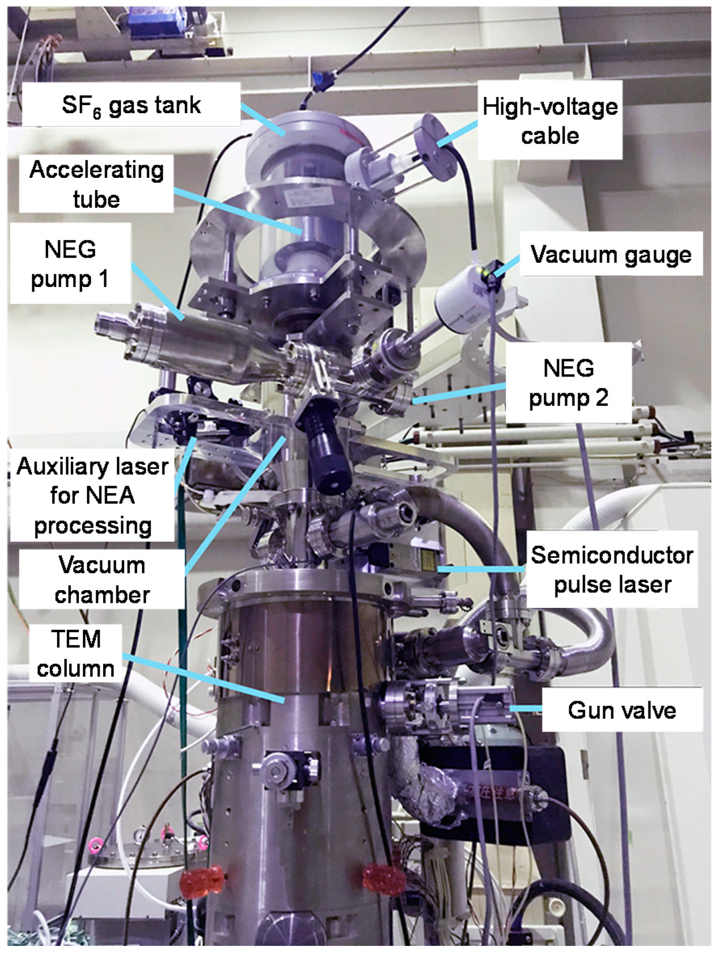
Figure 2 shows the appearance of a pulse TEM equipped with the developed photocathode electron gun. The pulsed electron gun consists of an ultrahigh vacuum chamber capable of NEA surface processing, an acceleration tube, an ion pump, two non-evaporable getter (NEG) pumps, a Cs vapor deposition source for NEA surface processing, a semiconductor pulse laser for pulse electron generation, and an auxiliary laser for photocurrent measurement during NEA surface processing. The accelerating voltage is 50 kV, and the ultimate vacuum of the chamber is ~5 × 10
−9 Pa. The wavelength of the semiconductor pulse laser for pulse electron generation is 404 nm, and it is possible to generate pulses from continuous wave (CW) to nanoseconds. The pulse electron gun was assembled by installing it to the Hitachi HF-2000 TEM (Hitachinaka, Ibaraki, Japanc) from which the cold field-emission electron gun and the acceleration tube were removed.
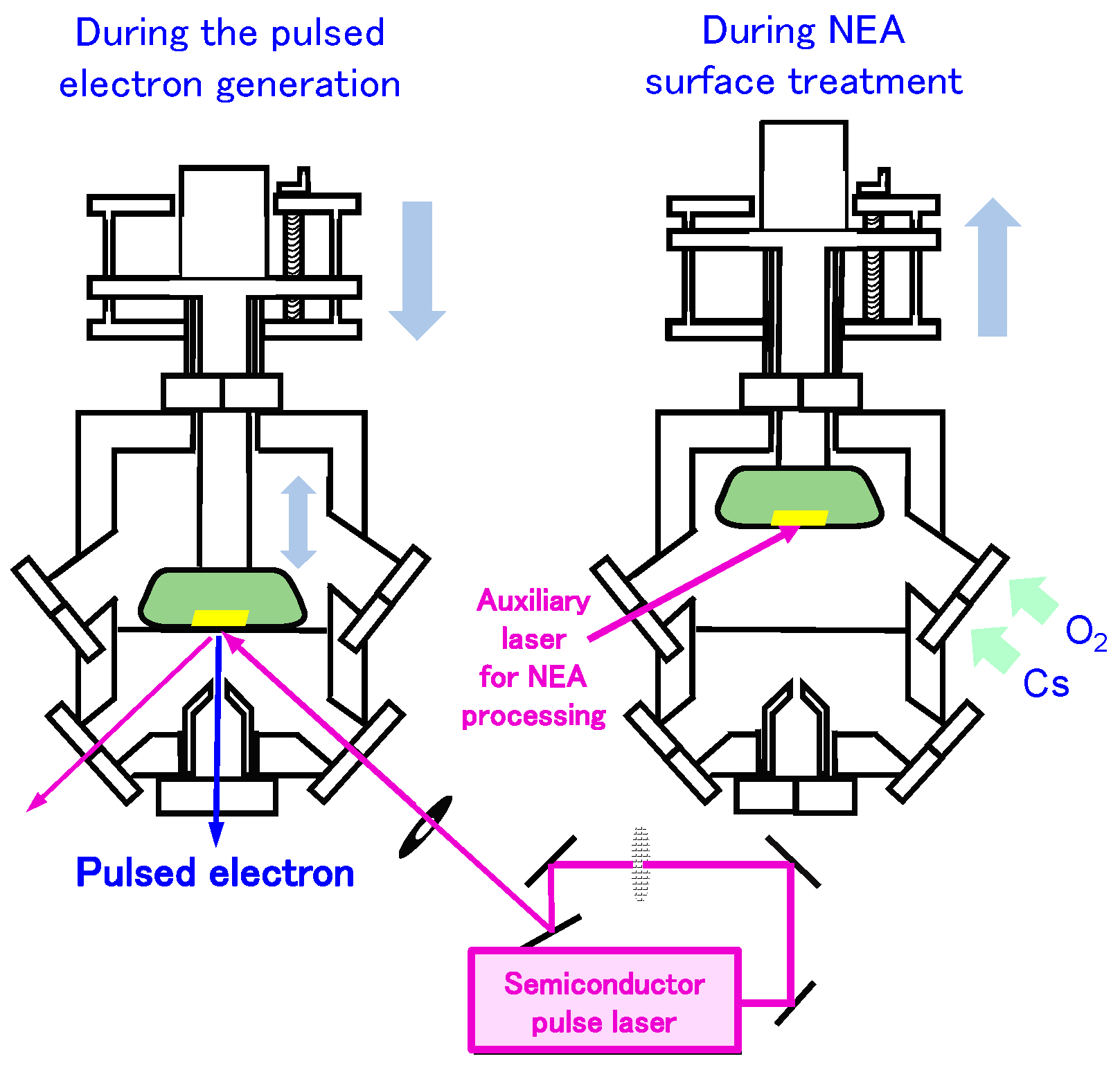
Figure 3 shows schematic illustrations of the operation. The cathode and acceleration tube have a structure that slides up and down. During the pulsed electron generation, the cathode and the anode are in a close state, and the pulsed electrons excited by the semiconductor pulse laser are introduced into the TEM column. On the other hand, during NEA surface treatment, the cathode moves to the upper part of the chamber, and the cathode substrate is heated at approximately 550 °C in an O
2 atmosphere of about 10
−6 Pa and under Cs vapor deposition. At the same time, the activation process is performed while monitoring the state with the photocurrent generated by the auxiliary laser excitation.
The cathode substrate is a p-type InGaN thin film. An In0.12Ga0.88N thin film doped with Mg with a thickness of about 250 nm is deposited on the sapphire substrate via a GaN buffer layer with a thickness of about 2.2 mm. In order to evaluate the performance of the apparatus, a cathode substrate passed about 2 years or more from the NEA surface treatment was used. The electron emission current immediately after the NEA surface treatment is about 10~100 mA, but it remains 1 mA even after about 2 years or more. The imaging conditions were a laser pulse width of 100 ms and a repetition frequency of 5 kHz. An imaging plate was used for image recording.
3. Performance Characterization
In order to evaluate the performance of the apparatus, the exposure time required for pulse imaging was measured.
Figure 4 shows a bright-field image that was taken by conventional TEM with a thermal emitter and size dispersion of Au nanoparticles on an amorphous carbon film used for pulse imaging as a standard sample. The size distribution was fitted by the lognormal distribution function, and the average particle size was approximately 13 nm.
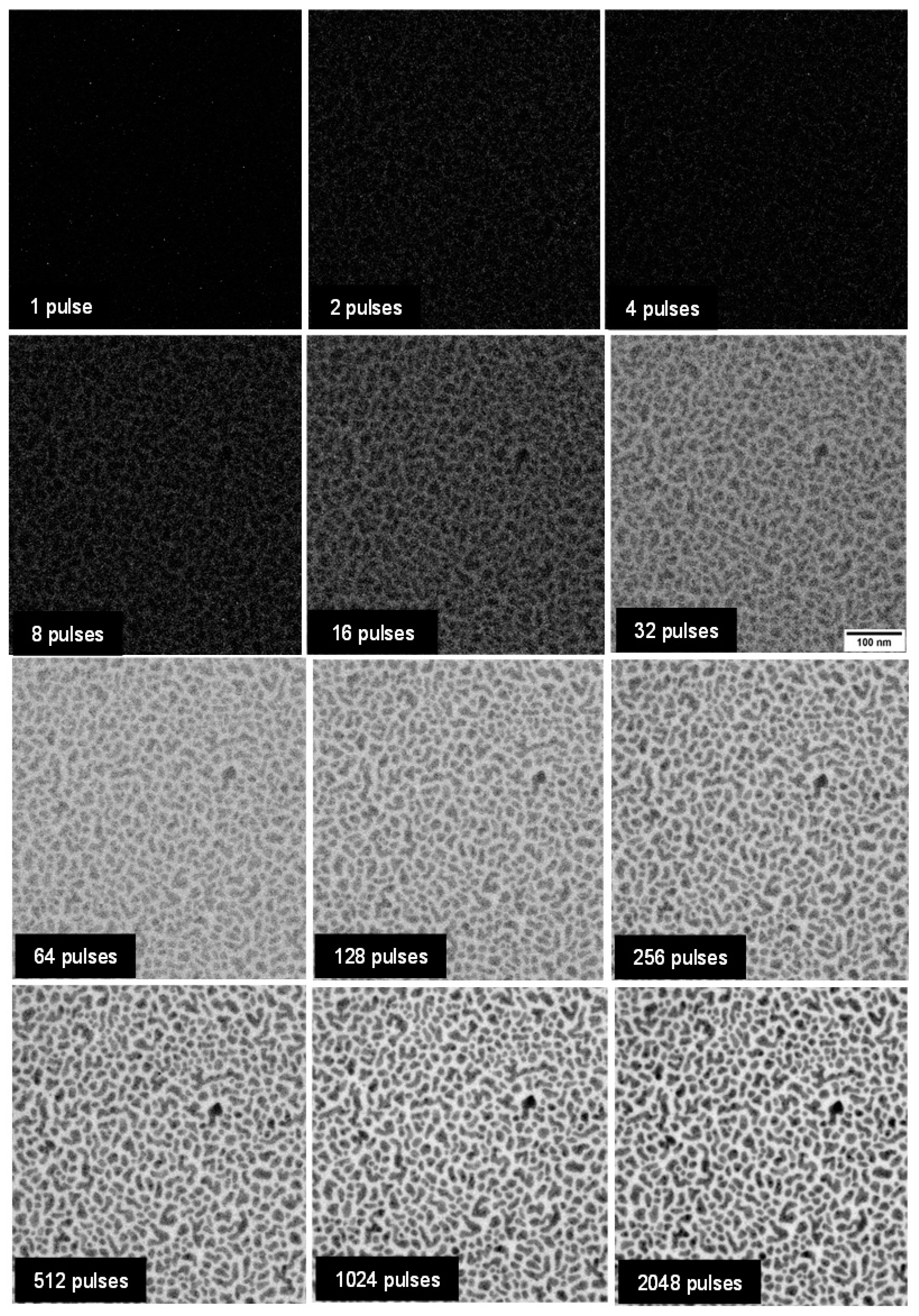
Figure 5 shows the results of the pulse imaging of Au nanoparticles mentioned above by bright-field images. The contrast becomes clearer as the number of integrated pulses increases. It is evident that the image can be identified at about 4–8 pulses under the conditions. A factor in which laser frequency affects image quality is the amount of specimen drift within the total exposure time. If the total exposure time is shortened, the effect of the specimen drift will be reduced, which will lead to an improvement in image quality. In
Figure 5, even with a total of 2048 pulses, the total exposure time is about 0.2 s, and even if an interval of 100 ms is included, it is 0.4 s, and the effect of the specimen drift is very small.
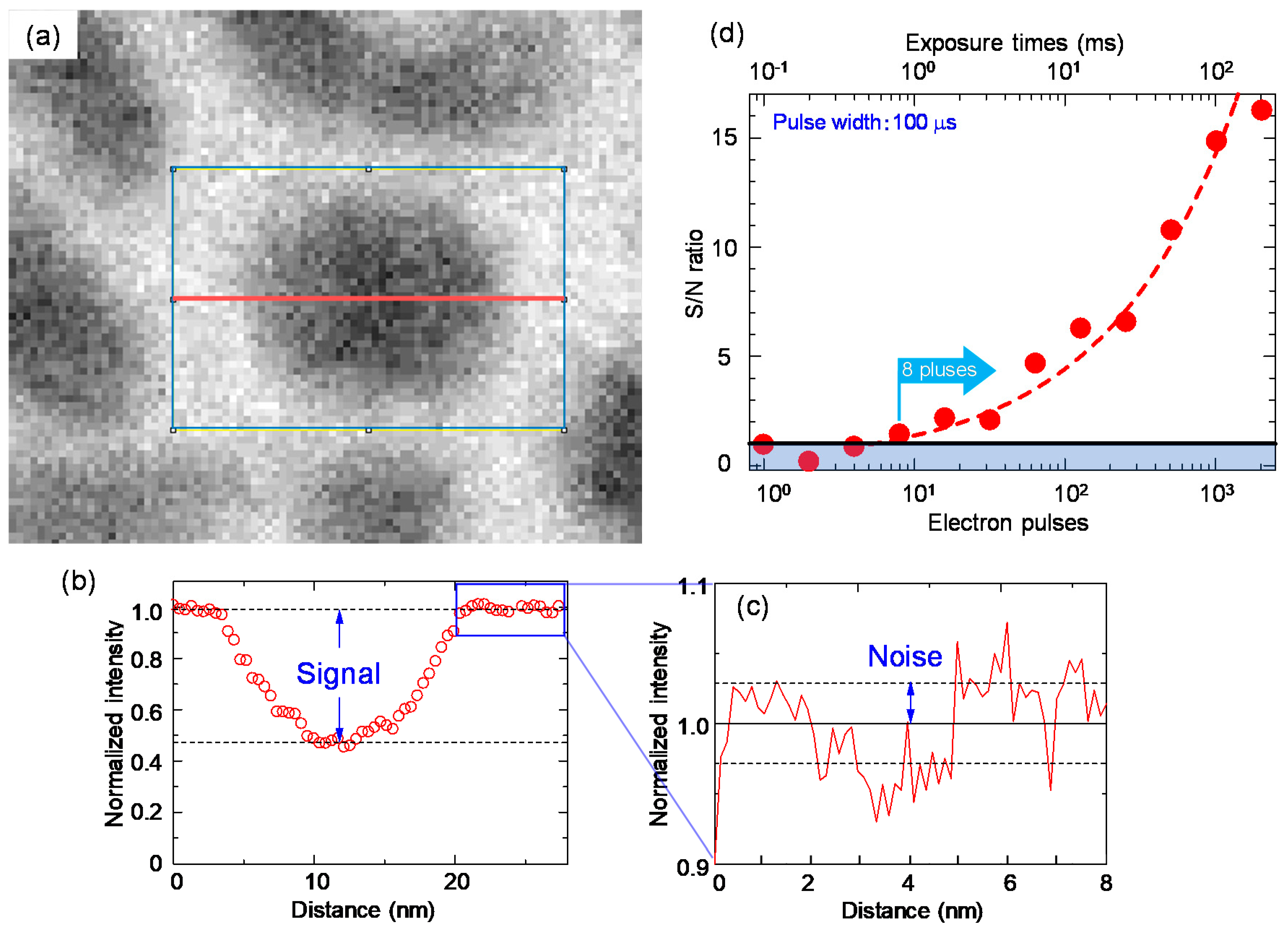
Figure 6 shows an example of the contrast profile of Au nanoparticles on an amorphous carbon support film. The contrast change of the part indicated by a red line in Au nanoparticles in
Figure 6a is shown in
Figure 6b. The dark contrast of the Au nanoparticle is shown as an image signal by normalization through the bright contrast of an amorphous carbon support film. An enlargement of the contrast in the amorphous carbon support film is shown in
Figure 6c. The deviation from the average value of the contrast is defined as noise.
Figure 6d shows the signal-to-noise (S/N) ratio as a function of the number of pulses (exposure time).
Based on this result, if the minimum exposure time is determined assuming that Au nanoparticles can be identified when the S/N ratio is 1 or more, it is revealed that an image can be recorded with an exposure time of 800 ms or more under the present condition. Immediately after NEA surface processing, which has a high quantum efficiency of the electron emission, it is possible to take an emission current that is one to two orders of magnitude larger, so it is considered that the minimum exposure time will be shorter. This performance suggests that it is sufficient for high-speed in situ observation as a pulsed TEM.
The performance of pulsed TEM mentioned above can also be applied to material nanofabrication. When a semiconductor photocathode is utilized as the electron gun of a semiconductor inspection device, the stability of the electron beam is extremely important. The required performance is a small current fluctuation, which is a standard deviation from the average current during a constant current generation for a long time. In particular, if the current fluctuation over a long time is large, it affects the performance, and the same accuracy as making the TEM image contrast negligibly small is required. It is considered that the fact that sufficient performance can be obtained by applying a semiconductor photocathode to a pulsed TEM is consistent with satisfying the necessary and sufficient conditions for utilizing a semiconductor photocathode in a semiconductor inspection device.
Recently, in the semiconductor manufacturing process, in order to solve the problems of low inspection throughput and drawing throughput, a new demand for higher brightness and a multi-electron beam source in which an individual source has high brightness and uniformity is searched. In order to obtain high brightness, an electron source that generates an electron beam with a large current and low-emittance characteristics is required. It is suggested that semiconductor photocathodes that enable the generation of a high-current, low-emittance, and high-speed pulse multi-electron beam are also useful as next-generation electron beam sources that respond to new demands of material nanofabrication.
4. Conclusions
We developed a TEM equipped with a NEA-InGaN photocathode electron gun with an accelerating voltage of 50 kV and evaluated its performance by imaging with a pulsed electron beam. The cathode has a long lifetime and can be imaged even after about 2 years of NEA surface treatment. Under the conditions, a bright-field image can provide an S/N ratio of 1 or more with an exposure time of 800 ms. By increasing the emittance further, the temporal and spatial resolutions can be improved.
Author Contributions
Conceptualization, T.N.; Data curation, S.I. and S.H.; Investigation, Y.H.; Writing—original draft, H.Y.; Writing—review & editing, H.A. All authors have read and agreed to the published version of the manuscript.
Funding
This work was supported by MEXT/JSPS KAKENHI, Grant Number JP19H00666, and by the joint research of “Research on observations by semiconductor photocathode electron beams”.
Conflicts of Interest
The funders had no role in the design of the study; in the collection, analyses, or interpretation of data; in the writing of the manuscript, or in the decision to publish the results.
References
- Chergui, M.; Zewail, A.H. Electron and X-ray methods of ultrafast structural dynamics: Advances and applications. ChemPhysChem 2009, 10, 28–43. [Google Scholar] [CrossRef] [PubMed]
- Bostanjoglo, O.; Elschner, R.; Mao, Z.; Nink, T.; WeingaKrtner, M. Nanosecond electron microscopes. Ultramicroscopy 2000, 81, 141–147. [Google Scholar] [CrossRef]
- Armstrong, M.R.; Reed, B.W.; Torralva, B.R.; Browning, N.D. Prospects for electron imaging with ultrafast time resolution. Appl. Phys. Lett. 2007, 90, 114101. [Google Scholar] [CrossRef] [Green Version]
- Barwick, B.; Park, H.S.; Kwon, O.-H.; Baskin, J.S.; Zewail, A.H. 4D Imaging of Transient Structures and Morphologies in Ultrafast Electron Microscopy. Science 2008, 322, 1227–1231. [Google Scholar] [CrossRef] [Green Version]
- Bücker, K.; Picher, M.; Crégut, O.; LaGrange, T.; Reed, B.W.; Park, S.T.; Masiel, D.J.; Banhart, F. Electron beam dynamics in an ultrafast transmission electron microscope with wehnelt electrode. Ultramicroscopy 2016, 171, 8–18. [Google Scholar]
- Sato, D.; Nishitani, T.; Honda, Y.; Amano, H. Observation of relaxation time of surface charge limit for InGaN photocathodes with negative electron affinity. Jpn. J. Appl. Phys. 2016, 55, 05FH05. [Google Scholar] [CrossRef]
- Kashima, M.; Sato, D.; Koizumi, A.; Nishitani, T.; Honda, Y.; Amano, H.; Iijima, H.; Meguro, T. Analysis of negative electron affinity InGaN photocathode by temperature-programed desorption method. J. Vac. Sci. Technol. B 2018, 36, 06JK02. [Google Scholar] [CrossRef]
- Sato, D.; Nishitani, T.; Honda, Y.; Amano, H. Recovery of quantum efficiency on Cs/O-activated GaN and GaAs photocathodes by thermal annealing in vacuum. J. Vac. Sci. Technol. B 2020, 38, 012603. [Google Scholar] [CrossRef]
- Sato, D.; Honda, A.; Koizumi, A.; Nishitani, T.; Honda, Y.; Amano, H. Optimization of InGaN thickness for high-quantum-efficiency Cs/O-activated InGaN photocathode. Microelectron. Eng. 2020, 223, 111229. [Google Scholar] [CrossRef]
- Kuwahara, M.; Kusunoki, S.; Jin, X.G.; Nakanishi, T.; Takeda, Y.; Saitoh, K.; Ujihara, T.; Asano, H.; Tanaka, N. 30-kV spin-polarized transmission electron microscope with GaAs–GaAsP strained superlattice photocathode. Appl. Phys. Lett. 2012, 101, 033102. [Google Scholar] [CrossRef]
- Kuwahara, M.; Kusunoki, S.; Nambo, Y.; Saitoh, K.; Jin, X.G.; Ujihara, T.; Asano, H.; Takeda, Y.; Tanaka, N. Coherence of a spin-polarized electron beam emitted from a semiconductor photocathode in a transmission electron microscope. Appl. Phys. Lett. 2014, 105, 193101. [Google Scholar] [CrossRef] [Green Version]
| Publisher’s Note: MDPI stays neutral with regard to jurisdictional claims in published maps and institutional affiliations. |
© 2021 by the authors. Licensee MDPI, Basel, Switzerland. This article is an open access article distributed under the terms and conditions of the Creative Commons Attribution (CC BY) license (http://creativecommons.org/licenses/by/4.0/).

 ,
, 