
Recent Progress in the Development of a-Se/CMOS Sensors for X-ray Detection
by
 , and
, and
Kaitlin Hellier
1, 
Emmie Benard
2 ,
,
Christopher C. Scott
3,
Karim S. Karim
3,4 and
Shiva Abbaszadeh
1,* 1
Electrical and Computer Engineering Department, University of California, 1156 High St., Santa Cruz, CA 95064, USA
2
Advanced Materials in the Quantum Age Laboratory, Arizona State University, 975 S. Myrtle Ave., Tempe, AZ 85281, USA
3
KA Imaging Inc., 560 Parkside Drive, Unit 3, Waterloo, ON N2L 5Z4, Canada
4
Waterloo Institute for Nanotechnology, University of Waterloo, 200 University Avenue West, Waterloo, ON N2L 3G1, Canada
*
Author to whom correspondence should be addressed.
Quantum Beam Sci. 2021, 5(4), 29; https://0-doi-org.brum.beds.ac.uk/10.3390/qubs5040029
Submission received: 1 August 2021
/
Revised: 4 October 2021
/
Accepted: 12 October 2021
/
Published: 18 October 2021
(This article belongs to the Special Issue X Rays: Physics and Applications)
Abstract
:Amorphous selenium (a-Se) is a glass-former capable of deposition at high rates by thermal evaporation over a large area. It was chosen as a direct conversion material due to its appealing properties for imaging in both low and high X-ray energy ranges (<30 keV and <30 keV, respectively). It has a bandgap of 2.2 eV and can achieve high photodetection efficiency at short wavelengths less than 400 nm which makes it appealing for indirect conversion detectors. The integration of a-Se with readout integrated circuits started with thin-film transistors for digital flat panel X-ray detectors. With increasing applications in life science, biomedical imaging, X-ray imaging, high energy physics, and industrial imaging that require high spatial resolution, the integration of a-Se and CMOS is one direct way to improve the high-contrast visualization and high-frequency response. Over the past decade, significant improvements in a-Se/CMOS technologies have been achieved with improvements to modulation transfer function and detective quantum efficiency. We summarize recent advances in integrating and photon-counting detectors based on a-Se coupled with CMOS readout and discuss some of the shortcomings in the detector structure, such as low charge conversion efficiency at low electric field and high dark current at high electric field. Different pixel architectures and their performance will be highlighted.
1. Introduction
Amorphous selenium (with a bandgap of approximately 2.2 eV) is one of the best photoconductors that was used in the photocopy industry. Its photogeneration efficiency was extensively studied during the sixties and seventies [1]. It was found that it has field-dependent mobility and conversion efficiency, which increase with increasing electric field [2]. Its main competitors (Si, PbO, CdTe, CdZnTe) suffer from spectral distortion due to issues of low detection efficiency (Si), K-fluorescence and cross-talk across pixels (CdTe, CdZnTe), despite low ionization energies and high carrier mobilities [3,4,5,6,7]. The polycrystalline nature of these materials also leads to issues of charge trapping from grain boundaries and defects, resulting in collection efficiency and polarization effects in the detectors and issues of scalability [8]. Amorphous selenium is also the only large area compatible avalanche-capable material.
Juska, et al. first observed the avalanche multiplication in a-Se in 1980 while they were studying the photogeneration efficiency and mobility of electrons and holes in a-Se at high electric fields [9]. Soon after that, a-Se was used in commercial ultrasensitive High-gain Avalanche Rushing Photoconductor (HARP) TV camera tubes [10,11]. HARP cameras demonstrated a higher signal-to-noise ratio in low-light conditions with the same exposure time compared to charged coupled device (CCD) cameras [12,13]. Although the impact ionization in a-Se was discovered some time ago and led to the commercialization of HARP cameras, this device has several drawbacks, including that (i) the readout mechanism requires a vacuum tube and (ii) crystallization of a-Se can occur in the long term, a concern for device stability [14]. Important issues in maintaining a high electric field within a-Se are the junction between metal, a-Se, and blocking layers, and their effects on the minimization of the dark current. The junction between metal and a-Se and its effects on the minimization of the dark current and device performance has received less attention in comparison to the well-studied charge transport and photogeneration mechanism in a-Se. Due to the device structure used in xerographic applications and in the HARP camera, this was not an important issue.
The application of a-Se in direct conversion flat panel X-ray detectors attracted interest to measure and understand the properties of the metal to a-Se junction, and studies have reported measurements on metal/a-Se/metal structures [15,16]. It was shown that the dark current is dependent on the voltage and changes by the nature of metal contacts, especially the positively biased contact. A proper hole blocking contact should have either a large potential barrier for holes between the positively biased metal contact and the a-Se layer, or a large number of hole traps and very low hole mobility. In addition, electrons should be able to flow freely through this hole-blocking layer. Most importantly, the layer should be compatible with the large area electronics and semiconductor fabrication processes. It was also shown that the substrate on which a-Se resides plays a role in crystallization, and the use of flexible substrates or blocking layers leads to greater stability and lifetimes in a-Se devices [17,18]. Conventional direct conversion a-Se based X-ray detectors, mainly used for mammography, are operating at 10 V/µm and there have been a few developments operating at higher fields up to 40 V/µm [19,20]. Efforts utilizing blocking layers have led to the stable application of high fields for achieving avalanche multiplication [21,22,23], with relatively low threshold fields of ~70 V/µm when compared to amorphous silicon, which requires fields up to 160 V/µm, and which overcome inherent issues in a-Se carrier mobility [24]. Alloying of a-Se has the potential for further reducing the threshold for avalanche, however further work in this area is required [25].
Understanding the junction of metal-amorphous selenium and its interface with blocking layers for increasing the electric field with a-Se to utilize avalanche multiplication has led to the emergence of a wide spectrum of new applications. For example, it has potential for use in life sciences and biomedical engineering applications [26] and various indirect and direct conversion medical X-ray imaging applications (e.g., fluoroscopy [27], positron emission tomography [28], and single-photon emission computed tomography [29]). In addition, it has the potential for applications in high energy physics (e.g., collider detectors) [30] and industrial imaging. The high UV sensitivity that can be achieved in a-Se alloys eliminates the complication of wavelength shifting in many applications such as large-scale time projection chambers.
For imaging applications, readout integrated circuits (ROICs) are a two-dimensional array of thin-film transistors (TFTs) or complementary metal-oxide-semiconductor (CMOS). The commercial a-Se flat panel X-ray detectors (e.g., Hologic and ANRAD) typically have 70–100 µm pixel apertures and utilize TFT technology. To target applications with small feature sizes (<25 µm) such as micro-angiography, mammography, intraoral, crystallography, protein analysis, and other small feature scientific imaging and machine vision applications, CMOS readout is preferred and more practical due to TFTs challenges associated with reduced pixel size. For example, moving to small pixels requires on-pixel amplifiers to improve the signal-to-noise ratio (SNR), which further limits the smallest TFT pixel size achievable. CMOS, on the other hand, is able to achieve small feature sizes and have comparable noise levels to CCDs, and the pixel architecture can be designed for both integration and photon counting applications [31]. In addition, small detector elements enable over-sampling of image data and the possibility of implementing an anti-aliasing filter to improve high spatial frequency detective quantum efficiency (DQE) and obtain dose reduction by requiring shorter exposure times [23,32,33].
In this review article, we will summarize the progress made in a-Se on CMOS platforms over the last decade, covering low-energy (~10 to 30 keV) X-ray detection for applications such as mammography and a few applications at higher energy (>30 keV), such as synchrotron imaging.
2. Energy-Integrating Detectors
Energy integrating, or integration mode detectors (EIDs), accumulate charge from several events over some period of time, termed the integration time. X-rays absorbed by a-Se generate charge clouds—which scale with the photon energy—that are accumulated over the integration window and read out as a signal intensity. EIDs provide several advantages over photon-counting detectors. Photon counting detectors require amplification at the pixel level, giving rise to complex electronics and costly fabrication to achieve small pixel sizes. Where energy resolution is not required, such as in some high-flux applications for crystallography, EIDs offer the most effective way to achieve large-scale detector technologies.
After the first demonstrated integration of a-Se and CMOS electronics by Andre et al. [34], little progress was made in the development of a-Se/CMOS integrating detectors until the late 2000s. Indirect and direct passive pixel sensor (PPS) arrays demonstrated the possibility of a-Se/CMOS EIDs with improved spatial resolution, however, they were still limited by resolution lower than commercially available detectors and the high level of noise and slow readout inherent to PPS architectures [35,36].
2.1. Achieving High Resolution in a-Se/CMOS Imaging
Models produced by Hajdok et al. [37] on the role of X-ray processes of converter materials, combined with experimental results on a-Se devices, demonstrated that pixel pitch is the predominant limiter in spatial resolution of existing detectors. In CMOS devices, imaging technology has been limited by fabrication capabilities and cost in manufacturing; relatively recent advances in these areas have led to improved pixel size and the possibility of sensors capable of detecting small feature sizes.
Developments in improved resolution focus on the reduction of the pixel pitch and the use of active pixel sensors (APS), which have faster readout and greater SNR than PPS. In addition to Hajdok’s work on X-ray processes, Que and Rowlands [38] investigated the various roles of photoelectron range, incident X-ray obliquity, and charge transport in a-Se, determining that the lateral spread of charge due to diffusion and Coulomb repulsion are negligible. Kabir and Kasap [39] later demonstrated that deep traps play a dominant role in reduced spatial resolution through the modeling of charge spread due to trapped carriers and the calculation of modulation transfer functions (MTFs), directly compared to experimental results of CdZnTe detectors.
Building upon these works, Scott et al. [40] analyzed the resolution limitations specific to an a-Se/CMOS device with standard trapping characteristics and a 25 µm pixel pitch by calculating the MTFs and detective quantum efficiencies (DQEs) in detectors with varying conversion material thicknesses and pixel pitches exposed to a selection of relevant energies.
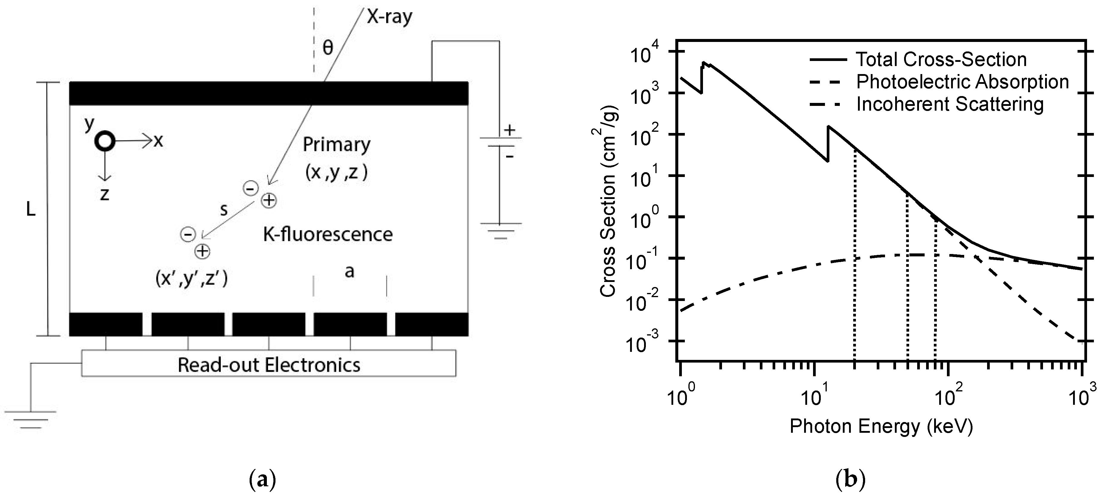
The model of the a-Se device used in these calculations is shown in Figure 1a). Pixels of aperture size a are covered by a layer of a-Se at thickness L, which is in turn coated with a top contact. The device is biased positively at the top electrode, generating an electric field across the device that results in hole collection at the pixels. X-rays are incident upon the device at some angle θ, which may be Compton scattered or photoelectrically absorbed at a primary point (x, y, z), generating an electron-hole pair; the photon cross-section for Se, illustrating the photoelectric absorption and scattering, can be seen in Figure 1b) [41]. If Compton scattered, the lower energy photon will be scattered and potentially absorbed elsewhere. The photoelectric effect may result in K-fluorescence, potentially exciting an additional pair at (x’, y’, z’) at a distance s away from the primary absorption point. The primary electron-hole pair results in several ionization events and a cloud of carriers, which are then transported to the pixel plane. Along the way, carriers may become trapped due to material defects, resulting in induced charge spread across the pixel plane. Collected carriers are averaged spatially based on the aperture at which they are collected.
Simulated MTFs were calculated by the transformations of point-spread functions (PSFs) and line-spread functions (LSFs) due to the charge spread from the primary photoelectron range, re-absorption from Compton scattering, reabsorption from K-fluorescence, obliquity of the incident X-rays, carrier trapping in the a-Se layer, and the aperture effect. In addition, DQE was modeled with the effects of X-ray attenuation, conversion gain, K-fluorescence, charge collection and trapping, aperture, noise aliasing, and electronic noise, as described in Kabir et al. [42]. Various thicknesses of the a-Se layer, pixel sizes, and incident X-ray energies were considered.
For a 200 µm thick a-Se system, decreasing the pixel size reduces the contribution of the aperture effect to reducing MTF values, pushing limiting factors toward X-ray interactions and the inherent limitations of the material such as trapping. A thicker a-Se layer of 1000 µm shows the greater effects of X-ray interactions for all pixel sizes, with obliquity playing a dominant role; with an incident angle of 0 degrees, the system again becomes limited by the aperture effect. Additional modeling by Hu et al. [43] reached similar conclusions on the role of a-Se thickness in MTF degradation with X-ray obliquity, despite the increase in DQE with thickness, experimentally verified with a-Se flat-panel imagers. Ultimately, Scott’s work shows that the 25-µm pitch provides the greatest spatial resolution in all cases, with the X-ray angle of incidence the greatest detriment to the improved performance. DQE at doses corresponding to various applications for the three different pixel pitches was evaluated with a noise of 300 electrons (rms), standard to CMOS at the time. In each case, the 25-µm pitch outperformed the larger pixels in spatial frequency, however, it is important to note that at low doses, the 25-µm pitch saw a significant reduction in DQE due to system noise. This work illustrates the potential of a-Se/CMOS devices in high-resolution imaging and the importance of reduced pixel size in the realization of this technology. It also set the stage for an understanding of the limiting factors and models in a-Se/CMOS imaging.
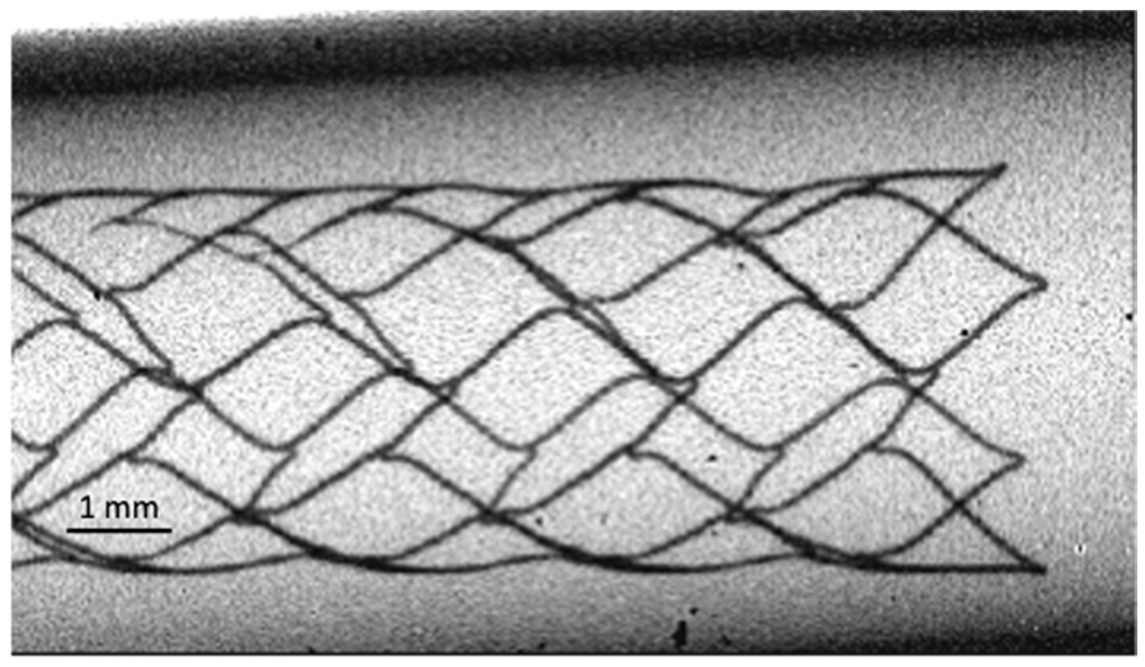
Confirmation of these models was later obtained by the development of an a-Se/CMOS 640 × 640 array with a 25 µm pixel pitch [44]. A CMOS three-transistor active pixel sensor (3T APS) was coated with a polyimide buffer layer, previously shown to reduce crystallization of the a-Se layer and serve as a blocking layer for hole injection [21]. This was followed by a 92 µm stabilized a-Se layer and a 50 nm gold top electrode. MTF was calculated from imaging with the slanted edge technique, using the straight edge of an opaque tungsten object at 40 kV [45,46]. Modeling results demonstrated that, as previously shown, the 25 µm pitch outperforms a commercially available 85 µm pitch at normal X-ray incidence. However, with some obliquity of the incoming X-rays, the performance of the 25 µm pitch degrades while the 85 µm pitch is largely unaffected. Even so, Scott demonstrated that the theoretical performance of the 25 µm pitch approaches the material limit for a-Se, and experimental results show good agreement with the model, the latter of which does not factor in measurement geometry and the energy profile of a real beam. In addition, they provided an image of an aortic stent measuring 25–50 µm, seen in Figure 2, demonstrating the spatial resolution of this detector.
Additional models [47] compared the theoretical performance of this a-Se/CMOS detector to existing micro-angiographic fluoroscopic (MAF) detectors. The Relative Object Detectability (ROD) family of metrics was calculated using MTF and DQE calculations, executed similarly as in Scott et al. [44], but includes factors such as geometric unsharpness, focal spot blurring, and scatter blur, which can lead to degraded detector performance. The a-Se detector was compared with MAF-CCD, MAF-CMOS, and flat-panel detector (FPD), previously reported. ROD values showed that a-Se significantly outperformed the other detectors, especially for the smallest objects modeled. However, the results demonstrate that increased magnification and focal spot blurring have detrimental effects on the a-Se detector performance. In order to maximize the MTF of the a-Se detector, a smaller focal spot size must be used and minimal magnification employed to reduce blurring.
Not only did the work of Scott et al. [40,44] and Russ et al. [47] demonstrate what was, at the time, the state of the art in X-ray detector spatial resolution, but it also set the stage for a deeper understanding of the X-ray interactions in a-Se devices in how they relate to the CMOS pixel array. The approach of comparing the measurement to models proved valuable in improving the performance of detectors, as can be seen in future work.
2.2. Further Improvements in Spatial Resolution by Pitch Reduction
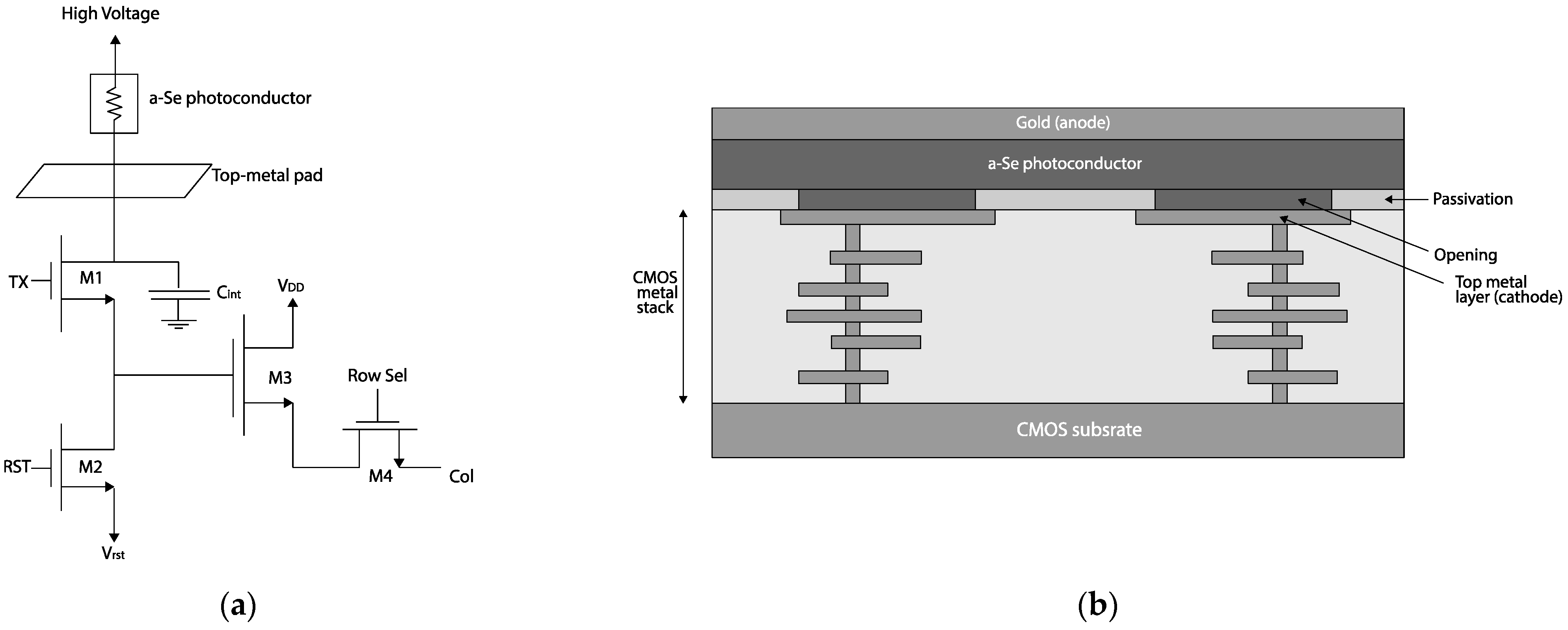
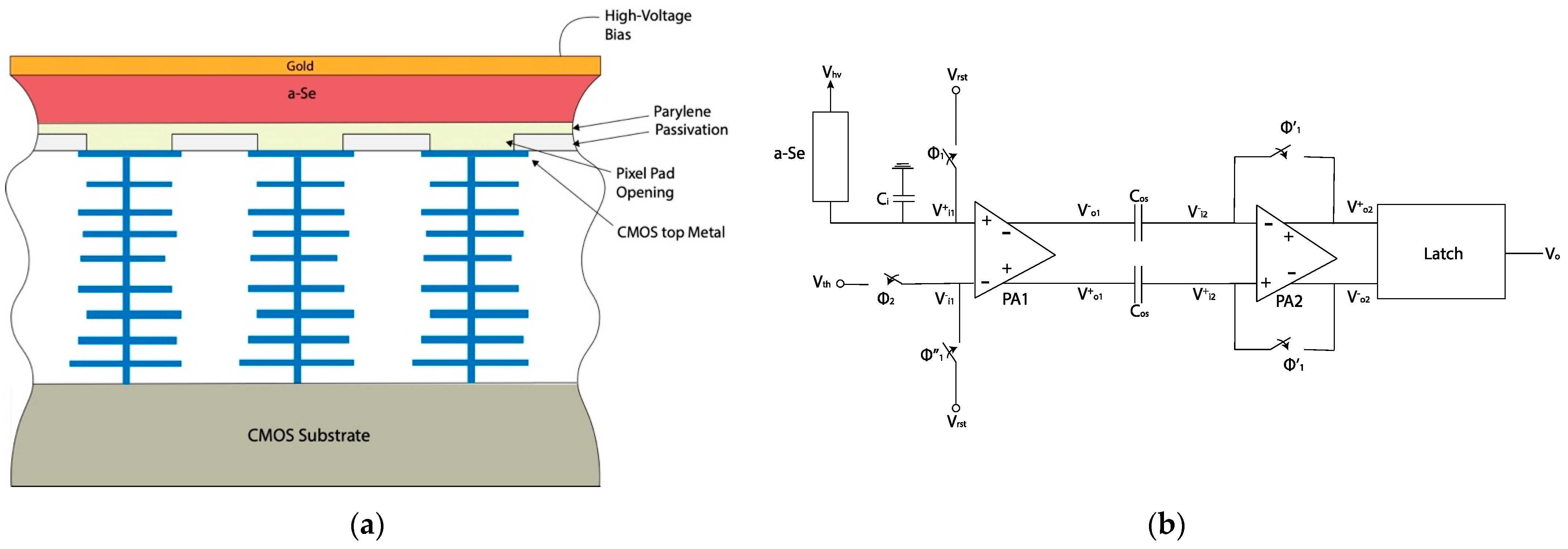
Further improvements in pixel pitch and spatial resolution were brought about by the development of custom 32 × 32 pixel arrays utilizing a CMOS four-transistor active pixel sensor (4T APS), the diagram of which can be seen in Figure 3a), with 5.6 µm × 6.25 µm pixel size. Parsafar et al. [48] describe the fabrication of the CMOS as a 6-metal 0.18 µm process with final dimensions of 3.0 mm × 1.8 mm. Stabilized a-Se with a thickness of 56 µm was deposited on top of the top-metal layer via a 4.1 µm × 4.8 µm opening in the passivation layer, and finally, a 30 nm thick gold was deposited to serve as a top electrical contact and was positively biased at 300 V. A cross-sectional view of the device architecture can be seen in Figure 3b).
An integration capacitor of 18 fF was incorporated into the 4T APS, and the small pixel capacitance reduced the pixel reset noise charge contribution. In addition, the use of a 4T APS allowed for correlated double sampling (CDS), further reducing noise by subtracting the reset voltage of the pixel from the voltage following integration [49]. With the 18 fF capacitor operated at 3.3 V, the pixel had a full well capacity (FWC) of 3.7 × 10⁵ electrons. At an integration time of 40 ms, the temporal noise due to photon shot noise and electronic noise was found to be approximately 350 electrons (rms), with a dark noise (due to random electronic noise only) at 90 electrons (rms). Initial results demonstrate X-ray responsivity and the measured MTF, calculated from the slanted edge technique imaging using a machined lead block, from which the MTF of 50% was extended from ~18 cycles/mm to 37 cycles/mm relative to Scott et al. [44]. Despite this critical improvement in resolution, the device still suffered from an un-optimized a-Se thickness and experimental challenges including edge imperfections and source-imager misalignment.
Following up on this work, Scott et al. [50] further evaluated the MTF, DQE, and dose efficiency of this device. MTF resulted in a reduction of spatial frequency at 50% to 32 cycles/mm and a mismatch between experiment and theory. The model, however, did not account for focal spot blurring, and when incorporated showed agreement with measurement, indicating that improvements to X-ray focal spots or detector geometry could lead to improved resolution. DQE gave high values relative to other works at the time at spatial frequencies up to 60 cycles/mm, showing promise for low-dose applications. Models indicate that optimization of the a-Se layer could further improve DQE.
Most recently, even greater improvements to the spatial resolution were achieved with a 1-megapixel detector comprised of 7.8 µm × 7.8 µm pixels, reported by Scott et al. [51]. This device reverts to a 3T APS design, shown in Figure 4a), with a 58 fF integration capacitance and an FWC of 8.33 × 10⁵ electrons. Despite the lack of CDS, combined with a mixed-signal process technology node and long integration time, the total readout noise was 180 electrons (rms).
The remainder of the device consisted of 100 µm of stabilized a-Se biased at 5–10 V/µm via a top electrode. The author highlights that the device can function as either a hole or electron collector but was specifically designed for hole collection due to the superiority of hole transport in a-Se and its stability of X-ray responsivity. Due to the large ratio of the a-Se thickness relative to the pixel pitch, the device exhibits the small pixel effect (SPE)—to be discussed in more detail in the following section—and therefore unipolar charge sensing, resulting in reduced lag. However, the lack of blocking layers was expected to contribute to an increased lag, possibly negating the effect of SPE.
The pixel array was characterized using monochromatic X-rays at energies of 21 keV and 63 keV, and linearity, responsivity, MTF, spatial resolving power, lag, and phase contrast were all evaluated. The response was found to be highly linear up to 26% and 34% full well capacity for 21 and 63 keV, respectively, with increased % FWC at higher energy due to a variety of factors, including a combination of higher energy photons, lower a-Se conversion gain at higher energy, and the possibility that the incident photon flux may have varied between energies. The responsivity with an applied bias of 4–5.8 V/µm resulted in reasonable agreement at the lower energy, however greater discrepancy at higher energy was not fully understood. MTF was again found using the slanted edge technique with a tungsten object; at 21 keV, the image could not be resolved due to beam non-uniformity, however, the 63 keV results showed degradation to 50% at ~30 cycles/mm, lower than previous works, but higher MTF at larger frequencies. Specifically, at the Nyquist frequency (64 cycles/mm), an MTF of 10% showed greater resolution than other direct conversion X-ray technologies. The spatial resolving power gave a contrast to noise ratio of ~10 for bars spaced at 8 µm in a JIMA RT RC-05 transmission bar target when sampled at 21 keV, the image of which can be seen in Figure 4b). Lag measurements indicated that lag was proportional to exposure, with the possibility that extra exposure reduces the a-Se responsivity, and enhanced injection charge recombined with trapped electrons, which, as previously stated, was not unexpected with no hole blocking layer. Finally, phase contrast edge enhancement was modeled and verified experimentally using an air bubble in an epoxy resin. Experimental results matched predictions, and they were able to estimate the bubble radius at 80 µm.
The authors believe that the high resolution and detection efficiency make their device unique compared to commercially available detectors and others reported in the literature. The ability to efficiently detect energies above 20 keV with high spatial resolution, not otherwise achievable, is especially exciting in areas such as materials science and particle physics, but slow detector speeds—frame rates of 5 fps—make the device non-competitive with many existing technologies in medical imaging, which utilize rates of >10 fps. The authors also argue that the consistency of these models and results, along with previous works, implies that they have a grasp on the X-ray interaction in a-Se, enabling even greater improvements to future devices.
As is the case of previous efforts, more work needs to be carried out, including incorporating blocking layers into the device architecture, which will improve lag, responsivity drift, conversion gain, and stabilization. Table 1 summarizes the developments in the EIDs discussed in this section, clearly demonstrating the effect of pixel pitch in spatial resolution. The continued reduction of pixel size, while increasing the array dimensions, can also lead to higher resolution and a greater field of view, adding to the competitiveness of these technologies. Of special interest for this device is its potential for single-photon counting, enabled by the SPE; as we will see in the next section, leveraging SPE can lead to lower dose rates and high resolution, enabling capabilities in medical fields such as angiography and mammography.
3. Single-Photon Detection
In order to resolve the finest features and maintain low doses required for medical treatments, detectors employ photon counting to resolve individual X-ray interactions and distinguish between incident energies. Photon-counting detectors (PCDs) register the generated charge for each X-ray interaction. After an electron-hole pair has been generated by the incident photon, the charge is collected, processed by a pre-amplifier and pulse shaper—which gives a pulse height corresponding to the energy of the photon—and an internal counter is incremented for the bin in which the energy falls. Multiple events within the readout window can lead to pile-up and false readings in energy and counts. SNR greater than five is required to allow detection of single events, and fast readout (<20 µs) is required for real-time measurements and single exposure dynamic imaging [52,53].
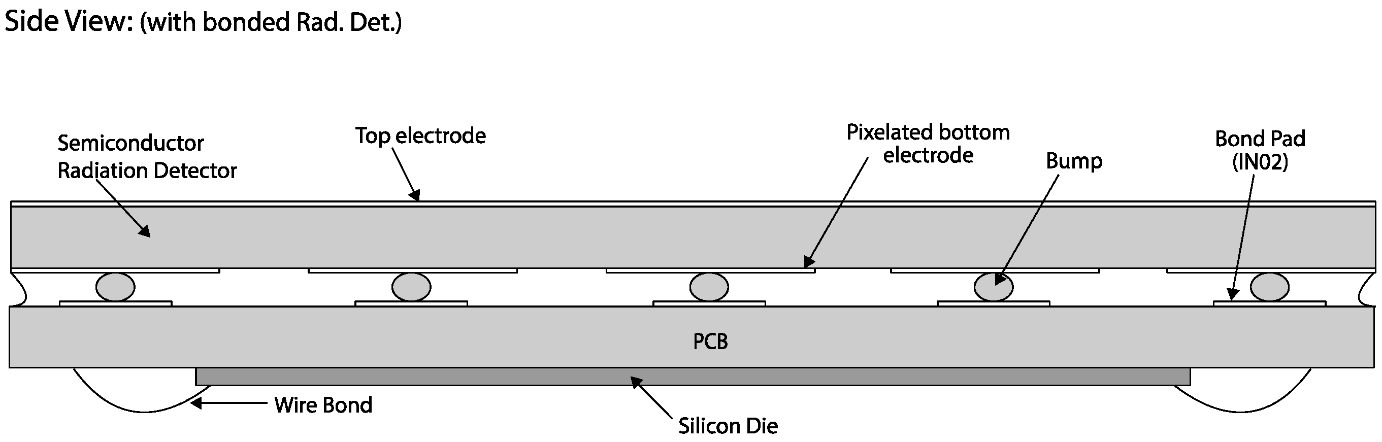
PCDs with a-Se are not a new concept; however, previous designs were limited by large pixel area and low readout speeds, preventing use in high-resolution, real-time applications. Goldan et al. [54] proposed a unique design for a single-photon counting (SPC) device targeting permanent breast seed implant (PBSI) insertion, allowing for resolution high enough and fast enough for increased accuracy of seed implantation. The system consisted of a 70 × 70 array of 1.4 mm pitch pixels bump bonded to a printed circuit board (PCB), subsequently wired to a CMOS chip, illustrated in Figure 5. Each pixel consisted of the radiation detector (the a-Se device) and CMOS components: a charge sensitive amplifier (CSA), a window comparator, a decision-making unit (DMU), a mode selector, and a pseudo-random counter. Simulations indicated that the system should provide a mean SNR of 8.7 for a 20 keV photon, great enough for the targeted application. However, the large pixel size limited further use.
Later work proposed a readout architecture that allowed both energy integration and photon counting, with a chip design that adapted to the incident radiation to switch between modes; lack of blocking layers limited the use in photon counting, despite some success in preliminary experiments [55]. In addition, Chen et al. [56] analyzed the feasibility of a-Se for SPC by modeling the X-ray photon interaction, detector geometry, charge transport, and pulse height shaping (PHS) and noise properties that play major roles in photon counting, and predicted PHS with low noise photon counting. This was experimentally verified, and high DQE levels were achieved. Due to low mobilities and applied fields, count rates were still low, though adequate for the targeted application of digital breast tomosynthesis.
Models performed by Tanguay et al. [57] suggested that SPC imaging generated DQEs greater than modeled EIDs, despite the impact of noise levels, but poor detection efficiency at greater a-Se thicknesses reversed this advantage. The author notes that these models did not include X-ray interaction effects, though the work contributed to the formalism describing noise power spectrum in SPC. Additional work in 2015 presented issues due to depth-dependent collection and double-counting interactions [58].
To fully reconcile the issue of low mobilities in a-Se and the need for high frame rate in photon counting, Goldan et al. [59] proposed the use of unipolar time-differential (UTD) charge sensing, where a local field is applied to increase the transport of the primary carrier and allowing for increased time resolution and collection of only the primary carrier. In this design, illustrated in Figure 6, Frisch grids are used to generate a near-field effect by applying VG, so that carriers generated in the bulk of the detector and drifting due to field VD are accelerated at the collector. The design was validated experimentally by depositing a-Se on a multi-well architecture developed using photolithography and demonstrated improved time resolution. Additional works in architectural design, including multi-well solid-state detectors (MWSD) and field-Shaping multi-Well Avalanche Detectors (SWAD) continued to utilize UTD and improve on spatial, energy, and time resolution, however fail to implement CMOS technologies and utilize the low noise and fast readout this provides.
Building on the improvements gained in unipolar charge sensing by utilizing the small pixel effect, Camlica et al. [60] and El Falou et al. [61] reported on an SPC detector comprised of two 26 × 196 arrays with 11 µm pitch pixels. Each pixel consists of a 70 µm thick stabilized a-Se layer deposited on a 0.5 µm thick parylene stabilization layer, which is opened to expose Al top-metal pads in the CMOS readout. Bias is applied to a-Se via a 50 nm thick Au top electrode at ~4 V/µm. No blocking layers are used, so noise from charge injection is not trivial. This design is illustrated in Figure 7a).
The large ratio of a-Se to pixel size generates the small pixel effect, where charge carriers are only detected at the pixel electrode once they are in close proximity [62]. This generates unipolar charge sensing as the minority carrier—in this case, electrons—is largely ignored by the pixel. Camlica took advantage of this effect to achieve a count rate of 5.5 × 10⁴ photons/s/pixel, greater than the 1.2 × 10⁴ required for mammography [63]. The simulated noise of the system is ~90 electrons (rms), and pulse-height spectroscopy measurements (PHS) lead to an estimated 7.2 counts/pixel for 60 keV photons. Verification using a 60 keV 241Am source gives an input-referred level of 190 electrons (rms) and an average of 5.5 counts/pixel, the former of which is attributed to interference in the particular chip tested. The author proposes that they are successful in the implementation of SPE for single-photon detection and that this work presents a route to SPC of a-Se/CMOS systems.
Additional work on this structure employs a blocking layer to prevent charge injection, reducing system noise [64]. Unfortunately, the fabrication required reduces the ability to produce the same pixel size, and the pitch is increased to 20 µm. They demonstrate a rise time of 150 ns, the fastest response reported for a-Se/CMOS detectors. Though promising, additional work has yet to be reported, limiting understanding of how this device architecture will perform in real applications and in comparison to existing detectors.
Photon counting a-Se detectors are still a very new technology relative to the development of a-Se, and much work must be carried out to characterize their imaging capabilities and realize their potential. However, a-Se SPC detectors show great progress and likely are soon to be ready for applications in imaging technology.
4. Conclusions and Considerations for Further Advancements in a-Se/CMOS Technology
Significant advancements were achieved over the last two decades in a-Se/CMOS technologies, guided by theoretical understanding and experimental verification of device limitations, and include reduced pixel size, architectural and circuit designs, which have led to improvements to MTF and DQE. The application of a-Se as a direct conversion X-ray detector enables high spatial resolution in many imaging fields, such as mammography, micro-angiography, intraoral imaging, and crystallography. Advances have largely been driven by the improvements to CMOS technologies, which continue at a rapid pace. In addition, future work in the incorporation of blocking layers and utilizing a-Se at a high electric field to achieve impact ionization opens the door to its applications as a photodetector for indirect conversion in positron emission tomography and high energy physics applications, such as collider detectors.
Though current detector technologies under commercial development are limited to integration detectors, major progress in photon-counting a-Se devices has been made. Initial results are promising, even if they are in preliminary stages; the work incorporating a-Se into small pixel CMOS technologies for these detectors is a large step in achieving the readout speeds required for distinguishing single events. The work undertaken in understanding interactions in a-Se integrating detectors sets the stage for rapid developments in single-photon counting devices.
Additional technologies such as multi-well solid-state detectors (MWSD), field-Shaping multi-Well Avalanche Detectors (SWAD), and apodized-aperture pixel (AAP) designs also provide unique opportunities for improving device architecture, and therefore performance in a-Se/CMOS detectors. Furthermore, developments on a-Se material properties and alloying have the potential to increase charge extraction and optical gain, reduce power consumption, and improve resolution in small pixel devices, making it even more competitive with existing commercial technologies. Even as it currently stands, a-Se integrated CMOS detectors have been shown to be viable technologies, with CMOS technology playing a vital role in this capability, and future developments sure to make a strong impact in a large array of applications.
Author Contributions
Conceptualization, K.H. and S.A.; investigation and analysis, K.H.; image generation, E.B.; writing—original draft preparation, K.H. and S.A.; writing—review and editing, E.B., C.C.S., K.S.K., S.A.; supervision, S.A.; funding acquisition, S.A. All authors have read and agreed to the published version of the manuscript.
Funding
This work was supported in part by the Department of Energy award DE-SC0021975 and by the UCSC REU program through National Science Foundation grant # 1950907.
Conflicts of Interest
The authors declare no conflict of interest.
References
- Kasap, S.; Frey, J.B.; Belev, G.; Tousignant, O.; Mani, H.; Laperriere, L.; Reznik, A.; Rowlands, J.A. Amorphous Selenium and Its Alloys from Early Xeroradiography to High Resolution X-ray Image Detectors and Ultrasensitive Imaging Tubes. Phys. Status Solidi B 2009, 246, 1794–1805. [Google Scholar] [CrossRef]
- Mort, J.; Pai, D.M.; Pai, C.M. Photoconductivity and Related Phenomena; Elsevier Scientific Publishing Company: Amerstdam, The Netherlands, 1976; ISBN 978-0-444-41463-2. [Google Scholar]
- Pellegrini, G.; Chmeissani, M.; Maiorino, M.; Blanchot, G.; Garcia, J.; Lozano, M.; Martinez, R.; Puigdengoles, C.; Ullan, M.; Casado, P. Performance Limits of a 55-µm Pixel CdTe Detector. IEEE Trans. Nucl. Sci. 2006, 53, 361–366. [Google Scholar] [CrossRef]
- Fredenberg, E.; Lundqvist, M.; Cederström, B.; Åslund, M.; Danielsson, M. Energy Resolution of a Photon-Counting Silicon Strip Detector. Nucl. Instrum. Methods Phys. Res. Sect. Accel. Spectrom. Detect. Assoc. Equip. 2010, 613, 156–162. [Google Scholar] [CrossRef]
- Iwanczyk, J.S.; Nygård, E.; Meirav, O.; Arenson, J.; Barber, W.C.; Hartsough, N.E.; Malakhov, N.; Wessel, J.C. Photon Counting Energy Dispersive Detector Arrays for X-ray Imaging. IEEE Trans. Nucl. Sci. 2009, 56, 535–542. [Google Scholar] [CrossRef] [PubMed] [Green Version]
- Barber, W.C.; Nygard, E.; Wessel, J.C.; Malakhov, N.; Wawrzyniak, G.; Hartsough, N.E.; Gandhi, T.; Iwanczyk, J.S. Fast Photon Counting CdTe Detectors for Diagnostic Clinical CT: Dynamic Range, Stability, and Temporal Response. In Proceedings of the Medical Imaging 2010: Physics of Medical Imaging, San Diego, CA, USA, 18 March 2010; SPIE: Bellingham, WA, USA, 2010; Volume 7622, pp. 465–472. [Google Scholar]
- Grynko, O.; Thibault, T.; Pineau, E.; Reznik, A. Engineering of a Blocking Layer Structure for Low-Lag Operation of the a-PbO-Based X-ray Detector. IEEE Trans. Electron Devices 2021, 68, 2335–2341. [Google Scholar] [CrossRef]
- Bolotnikov, A.E.; Camarda, G.C.; Wright, G.W.; James, R.B. Factors Limiting the Performance of CdZnTe Detectors. IEEE Trans. Nucl. Sci. 2005, 52, 589–598. [Google Scholar] [CrossRef]
- Juška, G.; Arlauskas, K. Impact Ionization and Mobilities of Charge Carriers at High Electric Fields in Amorphous Selenium. Phys. Status Solidi A 1980, 59, 389–393. [Google Scholar] [CrossRef]
- Maruyama, E. Amorphous Built-in-Field Effect Photoreceptors. Jpn. J. Appl. Phys. 1982, 21, 213. [Google Scholar] [CrossRef]
- Tanioka, K.; Yamazaki, J.; Shidara, K.; Taketoshi, K.; Kawamura, T.; Ishioka, S.; Takasaki, Y. An Avalanche-Mode Amorphous Selenium Photoconductive Layer for Use as a Camera Tube Target. IEEE Electron Device Lett. 1987, 8, 392–394. [Google Scholar] [CrossRef]
- Tanioka, K. High-Gain Avalanche Rushing Amorphous Photoconductor (HARP) Detector. Nucl. Instrum. Methods Phys. Res. Sect. Accel. Spectrom. Detect. Assoc. Equip. 2009, 608, S15–S17. [Google Scholar] [CrossRef]
- Tanioka, K. Development of Ultrahigh-Sensitivity HARP Pickup Tube and Its Applications. Int. Conf. Mach. Vis. Appl. 2013, 7, 173–176. [Google Scholar]
- Reznik, A.; Lui, B.J.M.; Lyubin, V.; Klebanov, M.; Ohkawa, Y.; Matsubara, T.; Miyakawa, K.; Kubota, M.; Tanioka, K.; Kawai, T.; et al. The Effect of Temperature on Photoinduced Metastability in Avalanche a-Se Layers. J. Non-Cryst. Solids 2006, 352, 1595–1598. [Google Scholar] [CrossRef]
- Johanson, R.E.; Kasap, S.O.; Rowlands, J.; Polischuk, B. Metallic Electrical Contacts to Stabilized Amorphous Selenium for Use in X-ray Image Detectors. J. Non-Cryst. Solids 1998, 227–230, 1359–1362. [Google Scholar] [CrossRef]
- Polischuk, B.T.; Shukri, Z.; Legros, A.; Rougeot, H. Selenium Direct-Converter Structure for Static and Dynamic X-ray Detection in Medical Imaging Applications. In Proceedings of the Medical Imaging 1998: Physics of Medical Imaging, San Diego, CA, USA, 24 July 1998; SPIE: Bellingham, WA, USA, 1998; Volume 3336, pp. 494–504. [Google Scholar]
- Abbaszadeh, S.; Rom, K.; Bubon, O.; Weinstein, B.A.; Karim, K.S.; Rowlands, J.A.; Reznik, A. The Effect of the Substrate on Transient Photodarkening in Stabilized Amorphous Selenium. J. Non-Cryst. Solids 2012, 358, 2389–2392. [Google Scholar] [CrossRef]
- Lindberg, G.P.; O’Loughlin, T.; Gross, N.; Mishchenko, A.; Reznik, A.; Abbaszadeh, S.; Karim, K.S.; Belev, G.; Weinstein, B.A. Photo-Crystallization in a-Se Layer Structures: Effects of Film-Substrate Interface-Rigidity. J. Appl. Phys. 2014, 116, 193511. [Google Scholar] [CrossRef]
- Ogusu, K.; Nakane, O.; Igasaki, Y.; Okamura, Y.; Yamada, S.; Hirai, T. Advanced a-Se Film with High Sensitivity and Heat Resistance for X-ray Detectors. In Proceedings of the Medical Imaging 2009: Physics of Medical Imaging, Lake Buena Vista, FL, USA, 13 March 2009; SPIE: Bellingham, WA, USA, 2009; Volume 7258, pp. 1135–1144. [Google Scholar]
- Zentai, G.; Partain, L.; Richmond, M.; Ogusu, K.; Yamada, S. 50 µm Pixel Size a-Se Mammography Imager with High DQE and Increased Temperature Resistance. In Proceedings of the Medical Imaging 2010: Physics of Medical Imaging, San Diego, CA, USA, 18 March 2010; SPIE: Bellingham, WA, USA, 2010; Volume 7622, pp. 385–393. [Google Scholar]
- Abbaszadeh, S.; Allec, N.; Ghanbarzadeh, S.; Shafique, U.; Karim, K.S. Investigation of Hole-Blocking Contacts for High-Conversion-Gain Amorphous Selenium Detectors for X-ray Imaging. IEEE Trans. Electron Devices 2012, 59, 2403–2409. [Google Scholar] [CrossRef]
- Abbaszadeh, S.; Tari, A.; Wong, W.S.; Karim, K.S. Enhanced Dark Current Suppression of Amorphous Selenium Detector With Use of IGZO Hole Blocking Layer. IEEE Trans. Electron Devices 2014, 61, 3355–3357. [Google Scholar] [CrossRef]
- Stavro, J.; Goldan, A.H.; Zhao, W. Photon Counting Performance of Amorphous Selenium and Its Dependence on Detector Structure. In Proceedings of the Medical Imaging 2018: Physics of Medical Imaging, Houston, TX, USA, 9 March 2018; SPIE: Bellingham, WA, USA, 2018; Volume 10573, p. 105735Y. [Google Scholar]
- Reznik, A.; Baranovskii, S.D.; Rubel, O.; Juska, G.; Kasap, S.O.; Ohkawa, Y.; Tanioka, K.; Rowlands, J.A. Avalanche Multiplication Phenomenon in Amorphous Semiconductors: Amorphous Selenium versus Hydrogenated Amorphous Silicon. J. Appl. Phys. 2007, 102, 053711. [Google Scholar] [CrossRef] [Green Version]
- Park, W.-D.; Tanioka, K. Lag and Light-Transfer Characteristics of Amorphous Selenium Photoconductive Film with Tellurium-Doped Layer. Jpn. J. Appl. Phys. 2016, 55, 071401. [Google Scholar] [CrossRef]
- Abbaszadeh, S.; Karim, K.S.; Karanassios, V. Measurement of UV from a Microplasma by a Microfabricated Amorphous Selenium Detector. IEEE Trans. Electron Devices 2013, 60, 880–883. [Google Scholar] [CrossRef]
- Hunt, D.C.; Tousignant, O.; Rowlands, J.A. Evaluation of the Imaging Properties of an Amorphous Selenium-Based Flat Panel Detector for Digital Fluoroscopy. Med. Phys. 2004, 31, 1166–1175. [Google Scholar] [CrossRef]
- Reznik, A.; Lui, B.J.M.; Rowlands, J.A. An Amorphous Selenium Based Positron Emission Mammography Camera with Avalanche Gain. Technol. Cancer Res. Treat. 2005, 4, 61–67. [Google Scholar] [CrossRef] [Green Version]
- Adnani, S.; Pil-Ali, A.; Scott, C.C.; Karim, K.S. Monte Carlo Simulation of an Amorphous Selenium-Based Multi-Layer Photon-Counting Detector for SPECT Applications. In Proceedings of the Medical Imaging 2021: Physics of Medical Imaging, Online Only, 15 February 2021; SPIE: Bellingham, WA, USA, 2021; Volume 11595, p. 1159515. [Google Scholar]
- Barman, S.K.; Huda, M.; Asaadi, J.; Gramellini, E.; Nygren, D. Thermodynamic and Optoelectronic Properties of Ultra-Thin-Film Crystalline and Amorphous Selenium from a First-Principles Investigation. Presented at the APS March Meeting, Virtual, 15–19 March 2021. [Google Scholar]
- Graeve, T.; Weckler, G.P. High-Resolution CMOS Imaging Detector. In Proceedings of the Medical Imaging 2001: Physics of Medical Imaging, San Diego, CA, USA, 28 June 2001; SPIE: Bellingham, WA, USA, 2001; Volume 4320, pp. 68–76. [Google Scholar]
- Nano, T.F.; Escartin, T.; Ismailova, E.; Karim, K.S.; Lindström, J.; Kim, H.K.; Cunningham, I.A. MTF and DQE Enhancement Using an Apodized-Aperture X-ray Detector Design. Med. Phys. 2017, 44, 4525–4535. [Google Scholar] [CrossRef] [PubMed] [Green Version]
- Nano, T.F.; Scott, C.C.; Li, Y.; Con, C.; Karim, K.S.; Cunningham, I.A. Performance Evaluation of a Se/CMOS Prototype X-ray Detector with the Apodized Aperture Pixel (AAP) Design. In Proceedings of the Medical Imaging 2019: Physics of Medical Imaging, San Diego, CA, USA, 1 March 2019; SPIE: Bellingham, WA, USA, 2019; Volume 10948, p. 1094816. [Google Scholar]
- Andre, M.P.; Spivey, B.A.; Martin, P.J.; Morsell, A.L.; Atlas, E.; Pellegrino, T. Integrated CMOS-Selenium X-ray Detector for Digital Mammography. In Proceedings of the Medical Imaging 1998: Physics of Medical Imaging, San Diego, CA, USA, 24 July 1998; SPIE: Bellingham, WA, USA, 1998; Volume 3336, pp. 204–209. [Google Scholar]
- Hristovski, C.; Goldan, A.; Majid, S.H.; Wang, K.; Shafique, U.; Karim, K. Characterization and Comparison of Lateral Amorphous Semiconductors with Embedded Frisch Grid Detectors on 0.18 µm CMOS Processed Substrate for Medical Imaging Applications. In Proceedings of the Medical Imaging 2011: Physics of Medical Imaging, Lake Buena Vista, FL, USA, 16 March 2011; SPIE: Bellingham, WA, USA, 2011; Volume 7961, p. 79610Q. [Google Scholar]
- Majid, S.H.; Goldan, A.H.; Hadji, B.; Belev, G.; Kasap, S.; Karim, K.S. Selenium Coated CMOS Passive Pixel Array for Medical Imaging. In Proceedings of the Medical Imaging 2011: Physics of Medical Imaging, Lake Buena Vista, FL, USA, 15 March 2011; SPIE: Bellingham, WA, USA, 2011; Volume 7961, p. 79614L. [Google Scholar]
- Hajdok, G.; Battista, J.J.; Cunningham, I.A. Fundamental X-ray Interaction Limits in Diagnostic Imaging Detectors: Spatial Resolution. Med. Phys. 2008, 35, 3180–3193. [Google Scholar] [CrossRef]
- Que, W.; Rowlands, J.A. X-ray Imaging Using Amorphous Selenium: Inherent Spatial Resolution. Med. Phys. 1995, 22, 365–374. [Google Scholar] [CrossRef] [PubMed]
- Kabir, M.Z.; Kasap, S.O. Modulation Transfer Function of Photoconductive X-ray Image Detectors: Effects of Charge Carrier Trapping. J. Phys. Appl. Phys. 2003, 36, 2352–2358. [Google Scholar] [CrossRef]
- Scott, C.C.; Allec, N.; Karim, K.S. A Study of Factors Limiting Spatial Resolution Using a 25 Micron Pixel Pitch Direct-Detection Amorphous Selenium Imaging System. In Proceedings of the Medical Imaging 2012: Physics of Medical Imaging, San Diego, CA, USA, 3 March 2012; SPIE: Bellingham, WA, USA, 2012; Volume 8313, pp. 1655–1666. [Google Scholar]
- Berger, M.J.; Hubbell, J.H.; Seltzer, S.M.; Chang, J.; Coursey, J.S.; Sukumar, R.; Zucker, D.S.; Olsen, K. XCOM: Photon cross Sections Database. Available online: https://www.nist.gov/pml/xcom-photon-cross-sections-database (accessed on 30 September 2021).
- Kabir, M.Z.; Rahman, M.W.; Shen, W.Y. Modelling of Detective Quantum Efficiency of Direct Conversion X-ray Imaging Detectors Incorporating Charge Carrier Trapping and K-Fluorescence. IET Circuits Devices Syst. 2011, 5, 222. [Google Scholar] [CrossRef]
- Hu, Y.-H.; Scaduto, D.A.; Zhao, W. The Effect of Amorphous Selenium Thickness on Imaging Performance of Contrast Enhanced Digital Breast Tomosynthesis. In Proceedings of the Breast Imaging; Maidment, A.D.A., Bakic, P.R., Gavenonis, S., Eds.; Springer: Berlin/Heidelberg, Germany, 2012; pp. 9–16. [Google Scholar]
- Scott, C.C.; Abbaszadeh, S.; Ghanbarzadeh, S.; Allan, G.; Farrier, M.; Cunningham, I.A.; Karim, K.S. Amorphous Selenium Direct Detection CMOS Digital X-ray Imager with 25 Micron Pixel Pitch. In Proceedings of the Medical Imaging 2014: Physics of Medical Imaging, San Diego, CA, USA, 19 March 2014; SPIE: Bellingham, WA, USA, 2014; Volume 9033, p. 90331G. [Google Scholar]
- Samei, E.; Flynn, M.J.; Reimann, D.A. A Method for Measuring the Presampled MTF of Digital Radiographic Systems Using an Edge Test Device. Med. Phys. 1998, 25, 102–113. [Google Scholar] [CrossRef] [Green Version]
- Estribeau, M.; Magnan, P. Fast MTF Measurement of CMOS Imagers Using ISO 12333 Slanted-Edge Methodology. In Detectors and Associated Signal Processing, St. Etienne, France, 19 February 2004; SPIE: Bellingham, WA, USA, 2004; Volume 5251, pp. 243–252. [Google Scholar]
- Russ, M.; Shankar, A.; Jain, A.; Nagesh, S.V.S.; Ionita, C.N.; Scott, C.; Karim, K.S.; Bednarek, D.R.; Rudin, S. Quantitative Comparison Using Generalized Relative Object Detectability (G-ROD) Metrics of an Amorphous Selenium Detector with High Resolution Microangiographic Fluoroscopes (MAF) and Standard Flat Panel Detectors (FPD). In Proceedings of the Medical Imaging 2016: Physics of Medical Imaging, San Diego, CA, USA, 22 March 2016; SPIE: Bellingham, WA, USA, 2016; Volume 9783, pp. 954–962. [Google Scholar]
- Parsafar, A.; Scott, C.C.; El-Falou, A.; Levine, P.M.; Karim, K.S. Direct-Conversion CMOS X-ray Imager With 5.6 µm × 6.25 µm Pixels. IEEE Electron Device Lett. 2015, 36, 481–483. [Google Scholar] [CrossRef]
- El Gamal, A.; Eltoukhy, H. CMOS Image Sensors. IEEE Circuits Devices Mag. 2005, 21, 6–20. [Google Scholar] [CrossRef]
- Scott, C.C.; Parsafar, A.; El-Falou, A.; Levine, P.M.; Karim, K.S. High Dose Efficiency, Ultra-High Resolution Amorphous Selenium/CMOS Hybrid Digital X-ray Imager. In Proceedings of the 2015 IEEE International Electron Devices Meeting (IEDM), Washington, DC, USA, 7–9 December 2015; pp. 30.6.1–30.6.4. [Google Scholar]
- Scott, C.C.; Farrier, M.; Li, Y.; Laxer, S.; Ravi, P.; Kenesei, P.; Wojcik, M.J.; Miceli, A.; Karim, K.S. High-Energy Micrometre-Scale Pixel Direct Conversion X-ray Detector. J. Synchrotron Radiat. 2021, 28, 1081–1089. [Google Scholar] [CrossRef]
- Burgess, A.E. The Rose Model, Revisited. J. Opt. Soc. Am. A 1999, 16, 633. [Google Scholar] [CrossRef] [PubMed] [Green Version]
- Fredenberg, E. Spectral and Dual-Energy X-ray Imaging for Medical Applications. Nucl. Instrum. Methods Phys. Res. Sect. Accel. Spectrom. Detect. Assoc. Equip. 2018, 878, 74–87. [Google Scholar] [CrossRef]
- Goldan, A.H.; Karim, K.S.; Reznik, A.; Caldwell, C.B.; Rowlands, J.A. Photon Counting Readout Pixel Array in 0.18-µm CMOS Technology for on-Line Gamma-Ray Imaging of 103-Palladium Seeds for Permanent Breast Seed Implant (PBSI) Brachytherapy. In Proceedings of the Medical Imaging 2008: Physics of Medical Imaging, San Diego, CA, USA, 18 March 2008; SPIE: Bellingham, WA, USA, 2008; Volume 6913, p. 69130S. [Google Scholar]
- Goldan, A.H.; Hadji, B.; Karim, K.S.; DeCrescenzo, G.; Rowlands, J.A.; Tousignant, O.; Laperrière, L. A Counting and Integrating Pixel Readout Chip for Amorphous Selenium Direct Radiation Detectors for Medical Imaging Applications. In Proceedings of the Medical Imaging 2009: Physics of Medical Imaging, Lake Buena Vista, FL, USA, 14 March 2009; SPIE: Bellingham, WA, USA, 2009; Volume 7258, p. 72583K. [Google Scholar]
- Chen, Y.; Liu, B.; O’Connor, J.M.; Didier, C.S.; Glick, S.J. Characterization of Scatter in Cone-Beam CT Breast Imaging: Comparison of Experimental Measurements and Monte Carlo Simulation. Med. Phys. 2009, 36, 857–869. [Google Scholar] [CrossRef] [Green Version]
- Tanguay, J.; Yun, S.; Kim, H.K.; Cunningham, I.A. Cascaded-Systems Analyses of Photon-Counting X-ray Detectors. In Proceedings of the Medical Imaging 2013: Physics of Medical Imaging, Lake Buena Vista, FL, USA, 19 March 2013; SPIE: Bellingham, WA, USA, 2013; Volume 8668, p. 86680S. [Google Scholar]
- Tanguay, J.; Yun, S.; Kim, H.K.; Cunningham, I.A. Detective Quantum Efficiency of Photon-Counting X-ray Detectors. Med. Phys. 2015, 42, 491–509. [Google Scholar] [CrossRef] [PubMed]
- Goldan, A.H.; Rowlands, J.A.; Tousignant, O.; Karim, K.S. Unipolar Time-Differential Charge Sensing in Non-Dispersive Amorphous Solids. J. Appl. Phys. 2013, 113, 224502. [Google Scholar] [CrossRef]
- Camlica, A.; El-Falou, A.; Mohammadi, R.; Levine, P.M.; Karim, K.S. CMOS-Integrated Single-Photon-Counting X-ray Detector Using an Amorphous-Selenium Photoconductor with 11 × 11-µm2 Pixels. In Proceedings of the 2018 IEEE International Electron Devices Meeting (IEDM), San Francisco, CA, USA, 1–5 December 2018; pp. 32.5.1–32.5.4. [Google Scholar]
- El-Falou, A.; Camlica, A.; Mohammadi, R.; Levine, P.M.; Karim, K.S. A Monolithic Amorphous-Selenium/CMOS Single-Photon-Counting X-ray Detector. IEEE Trans. Electron Devices 2021, 68, 1746–1752. [Google Scholar] [CrossRef]
- Barrett, H.H.; Eskin, J.D.; Barber, H.B. Charge Transport in Arrays of Semiconductor Gamma-Ray Detectors. Phys. Rev. Lett. 1995, 75, 156–159. [Google Scholar] [CrossRef] [Green Version]
- Abbene, L.; Gerardi, G.; Principato, F.; Del Sordo, S.; Ienzi, R.; Raso, G. High-Rate X-ray Spectroscopy in Mammography with a CdTe Detector: A Digital Pulse Processing Approach. Med. Phys. 2010, 37, 6147–6156. [Google Scholar] [CrossRef]
- Camlica, A.; Lee, D.; Jang, H.; Arnab, S.M.; Fang, Y.; Kabir, M.Z.; Karim, K.S. Performance of Amorphous Selenium Based Unipolar Charge Sensing Detector for Photon-Counting X-ray Imaging. In Proceedings of the Medical Imaging 2020: Physics of Medical Imaging, Houston, TX, USA, 16–19 February 2020; Bosmans, H., Chen, G.-H., Eds.; SPIE: Bellingham, WA, USA, 2020; Volume 11312, p. 113120G. [Google Scholar]
Figure 1.
(a) Schematic of the a-Se device model used in Scott et al. [40]. (b) Photon cross-section for Se in the range of interest; vertical dotted lines highlight the energies used in the model discussed [41].

Figure 2.
Image of a 25–50 µm aortic stent taken with the 25 µm pitch detector in [44].
Figure 2.
Image of a 25–50 µm aortic stent taken with the 25 µm pitch detector in [44].

Figure 3.
(a) Diagram of the 32 × 32 pixel arrays utilizing a CMOS four-transistor active pixel sensor (4T APS) and (b) a cross-sectional view of CMOS/a-Se device architecture utilized in Parsafar et al. [48].
Figure 3.
(a) Diagram of the 32 × 32 pixel arrays utilizing a CMOS four-transistor active pixel sensor (4T APS) and (b) a cross-sectional view of CMOS/a-Se device architecture utilized in Parsafar et al. [48].

Figure 4.
(a) The 3T APS design of 1-megapixel detector comprised of 7.8 µm × 7.8 µm pixels; (b) image of contrast to noise ratio ~10 for bars spaced at 8 µm in a JIMA RT RC-05 transmission bar target when sampled at 21 keV, similar to that found in [51].
Figure 4.
(a) The 3T APS design of 1-megapixel detector comprised of 7.8 µm × 7.8 µm pixels; (b) image of contrast to noise ratio ~10 for bars spaced at 8 µm in a JIMA RT RC-05 transmission bar target when sampled at 21 keV, similar to that found in [51].

Figure 5.
Schematic of the bump bonded device from Goldan et al. (adapted from [54]).
Figure 5.
Schematic of the bump bonded device from Goldan et al. (adapted from [54]).

Figure 6.
Device architecture for unipolar time-differential charge sensing in the a-Se device found in [59].
Figure 6.
Device architecture for unipolar time-differential charge sensing in the a-Se device found in [59].

Figure 7.
(a) The improved a-Se/CMOS device design; (b) improved SPC detector design comprised of two 26 × 196 arrays with 11 µm pitch pixels.
Figure 7.
(a) The improved a-Se/CMOS device design; (b) improved SPC detector design comprised of two 26 × 196 arrays with 11 µm pitch pixels.


Table 1.
Summary of properties from the experimental EIDs reported in this review.
| Scott 2014 [44] | Parsafar 2015 [48] | Scott 2021 [51] | |
|---|---|---|---|
| Pixel Pitch | 25 µm | 5.6 µm | 7.8 µm |
| Array Size | 640 × 640 | 32 × 32 | 1000 × 1000 |
| a-Se Thickness | 92 µm | 56 µm | 100 µm |
| CMOS Design | 3T APS | 4T APS | 3T APS |
| Noise floor | 300–400 rms | 350 rms | 150 rms |
| Frequency @ MTF = 0.5 | 18 cyc./mm | 32 cyc./mm | 28 cyc./mm |
| X-ray Energy | 28 keV | 40 keV | 63 keV |
Publisher’s Note: MDPI stays neutral with regard to jurisdictional claims in published maps and institutional affiliations. |
© 2021 by the authors. Licensee MDPI, Basel, Switzerland. This article is an open access article distributed under the terms and conditions of the Creative Commons Attribution (CC BY) license (https://creativecommons.org/licenses/by/4.0/).
Share and Cite
MDPI and ACS Style
Hellier, K.; Benard, E.; Scott, C.C.; Karim, K.S.; Abbaszadeh, S. Recent Progress in the Development of a-Se/CMOS Sensors for X-ray Detection. Quantum Beam Sci. 2021, 5, 29. https://0-doi-org.brum.beds.ac.uk/10.3390/qubs5040029
AMA Style
Hellier K, Benard E, Scott CC, Karim KS, Abbaszadeh S. Recent Progress in the Development of a-Se/CMOS Sensors for X-ray Detection. Quantum Beam Science. 2021; 5(4):29. https://0-doi-org.brum.beds.ac.uk/10.3390/qubs5040029
Chicago/Turabian StyleHellier, Kaitlin, Emmie Benard, Christopher C. Scott, Karim S. Karim, and Shiva Abbaszadeh. 2021. "Recent Progress in the Development of a-Se/CMOS Sensors for X-ray Detection" Quantum Beam Science 5, no. 4: 29. https://0-doi-org.brum.beds.ac.uk/10.3390/qubs5040029