Article

Fundamental Investigation of Diamond Cutting of Micro V-Shaped Grooves on a Polycrystalline Soft-Brittle Material

Department of Mechanical Engineering, Faculty of Science and Technology, Keio University, 3-14-1 Hiyoshi, Kohoku-ku, Yokohama 223-8522, Japan
*
Author to whom correspondence should be addressed.
J. Manuf. Mater. Process. 2021, 5(1), 17; https://0-doi-org.brum.beds.ac.uk/10.3390/jmmp5010017
Submission received: 3 January 2021 / Revised: 4 February 2021 / Accepted: 4 February 2021 / Published: 8 February 2021
(This article belongs to the Special Issue Progress in Precision Machining)

Abstract

:
Fabricating micro-structures on optical materials has received great interest in recent years. In this work, micro-grooving experiments were performed on polycrystalline zinc selenide (ZnSe) to investigate the feasibility of surface micro-structuring on polycrystalline soft-brittle material by diamond turning. A photosensitive resin was coated on the workpiece before cutting, and it was found that the coating was effective in suppressing brittle fractures at the edges of the grooves. The effect of tool feed rate in groove depth direction was examined. Results showed that the defect morphology on the groove surface was affected by the tool feed rate. The crystallographic orientation of grains around the groove was characterized by electron backscatter diffraction (EBSD), and it was found that the formation of defects was strongly dependent on the angle of groove surface with respect to the cleavage plane of grain. The stress distribution of the micro-grooving process was investigated by the finite element method. Results showed that the location of tensile stresses in the coated workpiece was farther from the edge of the groove compared with that in the uncoated workpiece, verifying the experimental result that brittle fractures were suppressed by the resin coating.

1. Introduction

Many optical crystals, for example, potassium dihydrogen phosphate (KDP) [1], calcium fluoride (CaF2) [2], zinc sulphide (ZnS), and zinc selenide (ZnSe) [3], have relatively low hardness and high brittleness, which makes them very difficult to machine in a ductile mode. In addition, commercial optical elements are usually made of polycrystalline materials, for example polycrystalline zinc selenide (p-ZnSe), due to lower cost compared to single crystal materials. In bulk polycrystalline materials, all grains have various crystal orientations, which makes it difficult to achieve uniformly smooth surfaces by machining.
In recent years, the requirement for the performance of optical components is becoming higher and higher [4]. Fabrication of micro-structure on material surface attracted considerable attention because it can offer unique functions for optical components, such as enhancement of sensitivity [5], increased field of view [6], and miniaturisation of components [7]. Thus, creating micro-structure on polycrystalline soft-brittle materials is of great importance for optics applications.
The fabrication of micro-structured surfaces can be realized by a variety of non-mechanical methods, such as beam based processing, electrical machining, lithography, and chemically assisted manufacturing [8]. As one of the mechanical methods, ultraprecision diamond cutting is popularly used for micro-structure machining, because it can directly create complex micro-structured surface with high accuracy and surface quality [9,10]. For ultraprecision cutting of micro-structured surfaces on brittle materials, several studies have been conducted. Mukaida et al. [5,11] and Zhu et al. [12] successfully generated microlens arrays and structures with sinusoidal waves on single-crystal silicon wafers, respectively. Jasinevicius et al. [13] and Yan et al. [14] investigated diamond turning of Fresnel lenses on single-crystal InSb and germanium, respectively. However, the investigation of micro-structure cutting on polycrystalline soft-brittle materials are few.
Ductile machinability of polycrystalline soft-brittle material in ultraprecision diamond cutting has been reported for a flat surface under strictly controlled conditions [15]. However, cutting of micro-structured surfaces, in particular, micro V-shaped grooves, on polycrystalline soft-brittle material is more challenging due to the following reasons:
(1)
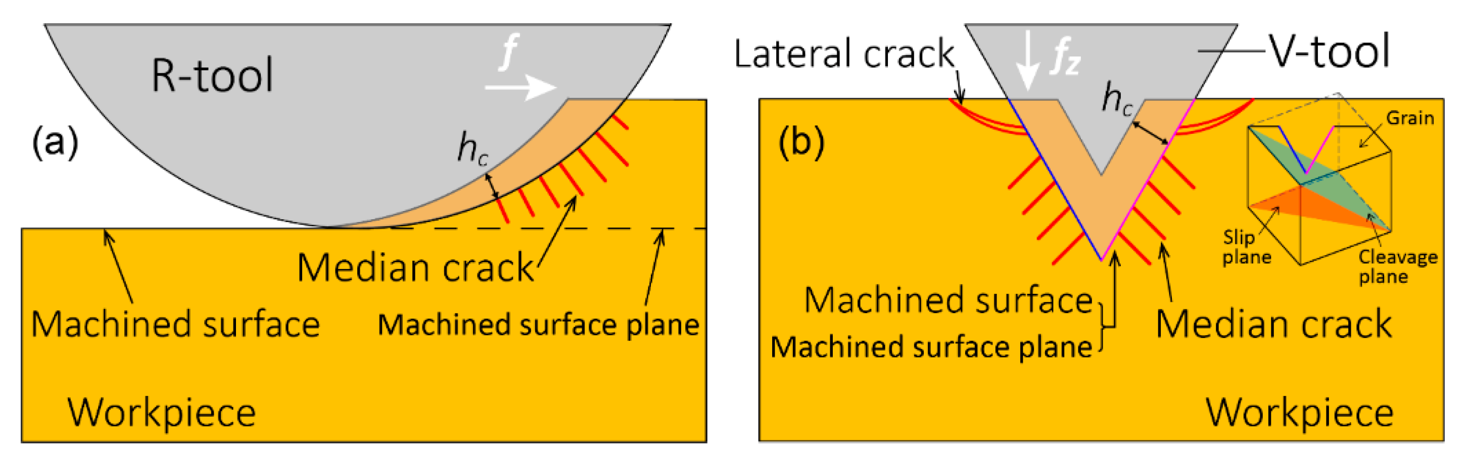
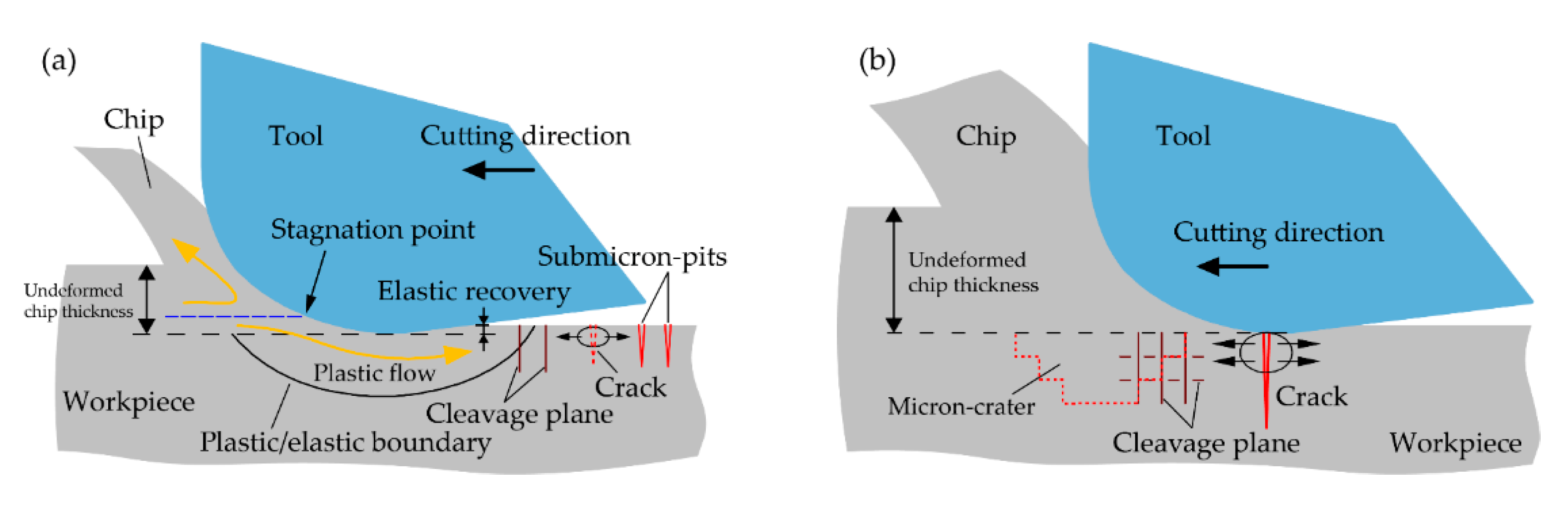
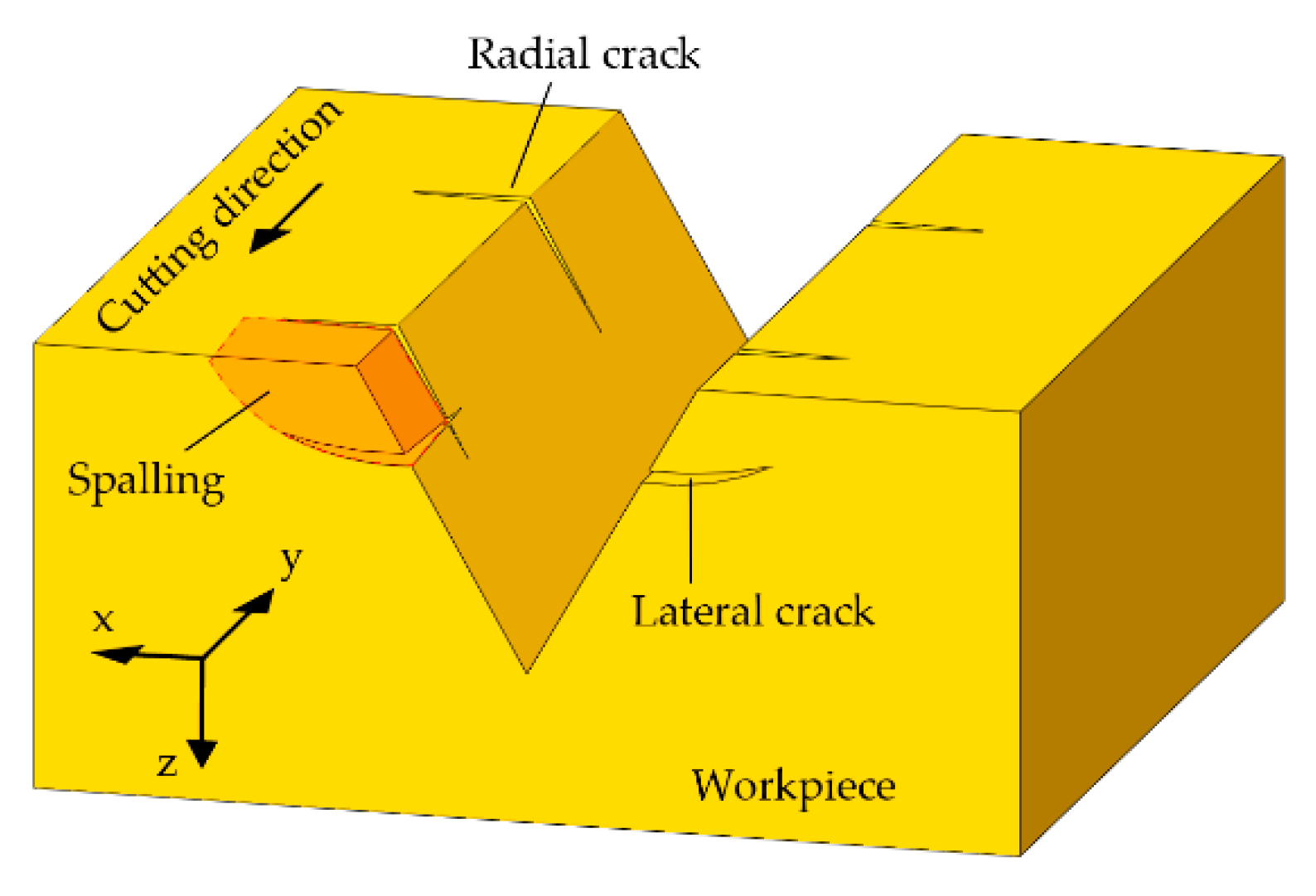
The conventional ductile-regime machining model is not applicable to cutting of V-shaped grooves. It is well known that in cutting of flat surfaces, crack-free machined surface can be generated even if the cracks occur during cutting process, as long as median cracks do not propagate to below the machined surface plane [16], as illustrated in Figure 1a. However, when cutting V-shaped grooves, if cracks are produced, the cracks will remain in the machined surface without being removed, as illustrated in Figure 1b. Thus, to achieve crack-free machined surface, the initiation of cracks must be completely suppressed.
(2)
High stress concentration occurs at the apex of groove edge. Existing research on machining V-shaped grooves has reported that high-stress region is located at the apex of groove edge [17,18]. Owing to the low fracture toughness of brittle materials, lateral cracks are likely to initiate at this region, causing material spalling, as illustrated in Figure 1b.
(3)
The two side surfaces of a V-shaped groove are in different relative positions with respect to the cleavage planes and slip planes of crystal grains, as illustrated in Figure 1b. Therefore, the material removal mechanism of the two sides of a V-shaped groove is likely different.
Pre-coating on the workpiece is considered as an effective method to improve the surface integrity in cutting of brittle materials. Heidari et al. [19] reported that injecting wax into the pores of porous silicon can suppress brittle fractures around the pores. The wax completely filling the pores help to resist hydrostatic pressure around the pores, and consequently prevent the propagation of cracks. Further, Lee et al. [20] reported that the critical undeformed chip thickness of crack generation in single-crystal CaF2 is increased, when applying permanent marker ink on the workpiece before cutting. They likewise attributed the reason to the compressive stresses provided by the solidified ink coating, which can suppress fluctuations of cutting force. Kalkhoran et al. [21] used a wax coating during the micro-grooving of single-crystal silicon and found that the wax coating improved the surface quality of the grooves. However, these studies did not clearly demonstrate the role of the coating on stress distribution in the workpiece. Besides, it is likewise unclear whether the pre-coating method is effective or not for groove cutting of polycrystalline soft brittle materials.
In this study, micro V-shaped grooves cutting experiments were performed on p-ZnSe to explore the feasibility of generating micro-structures on polycrystalline soft-brittle materials in a ductile mode. The machined surface integrity for uncoated workpiece and coated workpiece were compared with each other. Meanwhile, the effect of pre-coating on stress distribution in the workpiece during cutting was investigated by finite element simulation. Finally, the effect of grain orientation on surface integrity was investigated by electron backscatter diffraction (EBSD). The findings of this study will provide guidelines for surface integrity improvements in diamond cutting of micro-structured surfaces on polycrystalline soft-brittle materials.

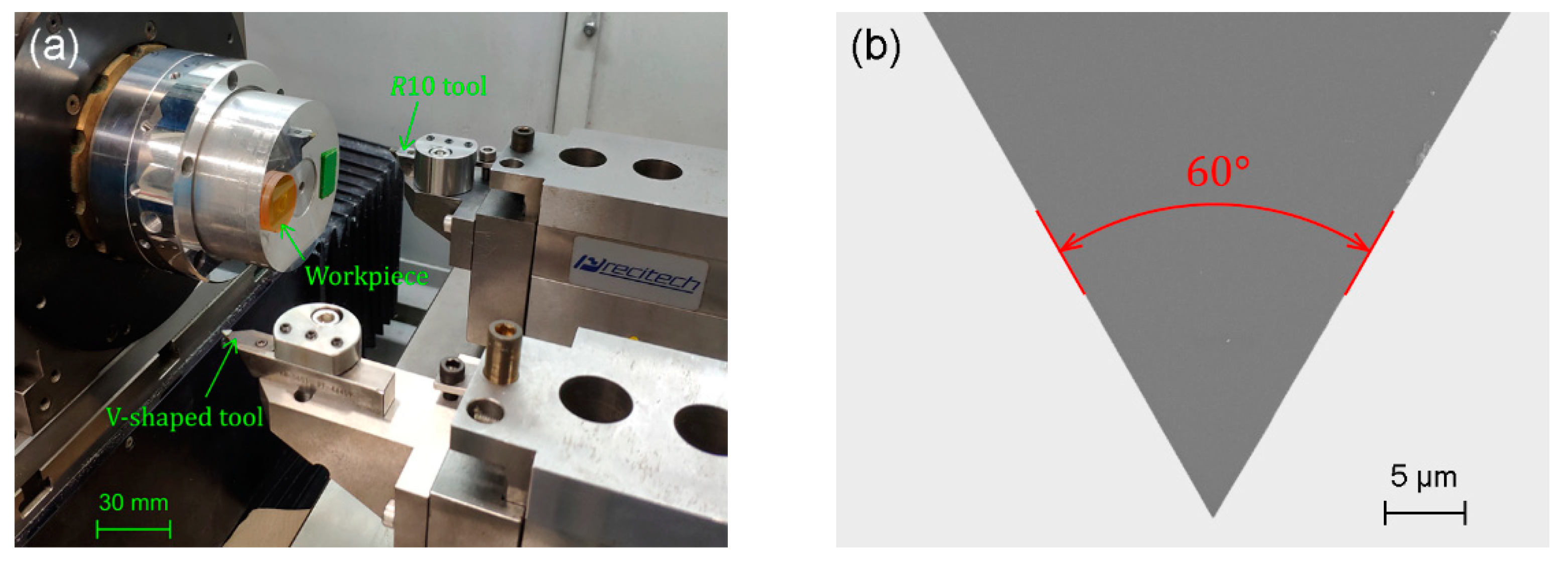
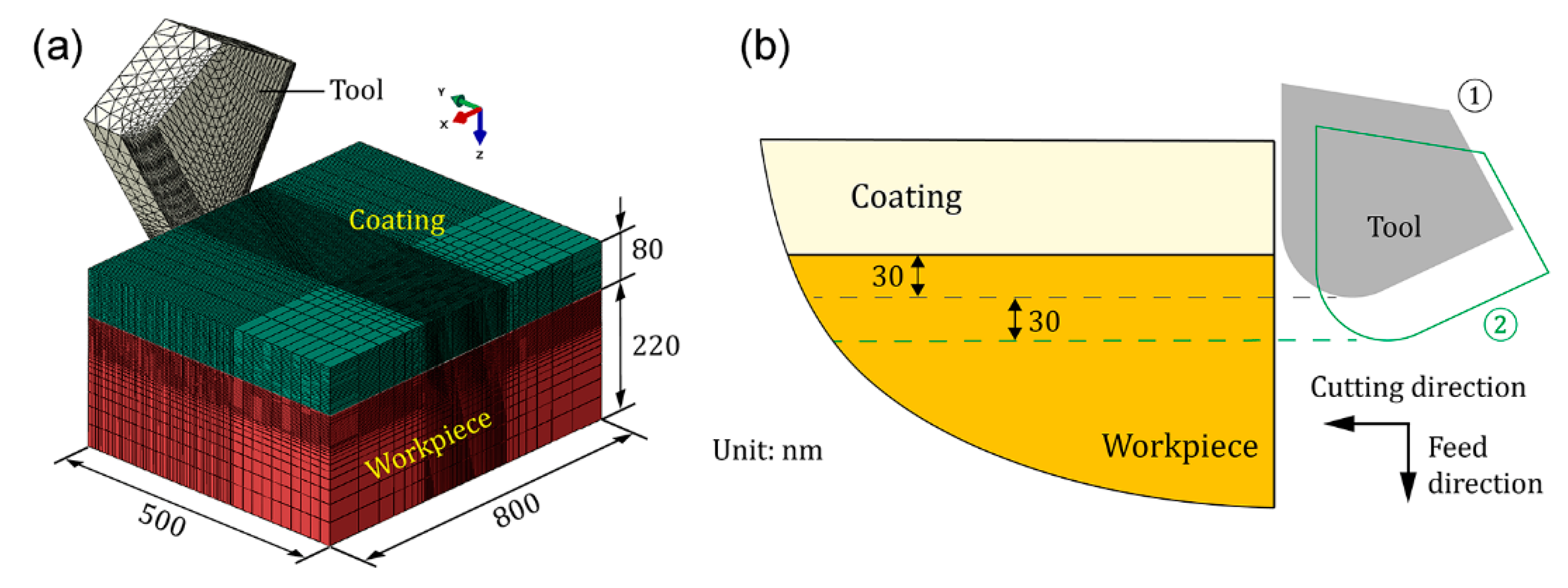
2. Materials and Methods

A chemical vapor deposited (CVD) ZnSe wafer was used as workpiece. The grain size of the workpiece ranges from 3 to 80 μm, and most grains are in the size of 30 to 50 μm. The material hardness and fracture toughness are 1.6 ± 0.3 GPa and 0.87 ± 0.15 MPa·m1/2, respectively. The characterization of microstructure distribution of the workpiece has been described in detail in our previous study [15].
The micro V-shaped grooves cutting experiment was performed on an ultraprecision lathe Nanoform X (AMETEK Precitech Inc., Keene, NH, USA). Figure 2a shows the experimental setup. The workpiece was fixed on an aluminum block, 20 mm away from the center of spindle. A single-crystal diamond V-shaped tool with an extremely sharpened tool tip and an included angle of 60° was used, the scanning electron microscope (SEM) image of which is shown in Figure 2b. The rake angle and relief angle of the tool are 0° and 5°, respectively. Before cutting the V-shaped grooves, a precut was performed by a diamond tool with a nose radius of 10 mm (R10 tool) to achieve a flat damage-free surface. To make sure that the coating can tightly adhere to the workpiece surface, and that the coating process can be done in situ, photosensitive resin was chosen as the coating material.
Figure 3 schematically shows the experimental procedures. First, V-shaped grooves were cut on the uncoated workpiece, as shown in Figure 3a,b. To cut a V-shaped groove, the tool was incrementally fed along negative z-direction with a distance of fz during the air-cutting period of each spindle revolution, until the depth of groove d reached the predetermined value. To ensure the feed of Z-slide of machine tools stable during the air-cutting period, the spindle rotation rate was set to 50 rpm. After cutting the V-shaped grooves on the uncoated workpiece, the workpiece surface was coated with photosensitive resin liquid. Followed by irradiating the resin with ultraviolet (UV) light for 30 min, the resin fully cured. Then, the cured resin was flattened and thinned by the R10 tool to a thickness of 20 μm, as illustrated in Figure 3c. Afterwards, other grooves were cut on the coated workpiece under the same condition as that used for cutting the uncoated workpiece, as shown in Figure 3d. Finally, the workpiece was cleaned by acetone in ultrasonic bath to remove the resin, as illustrated in Figure 3e. The machining parameters for the micro V-shaped grooves cutting experiment are summarized in Table 1. Due to the fact that zinc selenide is toxic, and it is difficult to remove chip debris by coolant flushing [22], all experiments were conducted under dry cutting condition, and the cutting chips were collected by vacuum suction during cutting.
After finishing the micro V-shaped grooves cutting experiment, the grooves were directly observed by a field-emission scanning electron microscope (FE-SEM), ZEISS MERLIN Compact (Carl Zeiss AG, Oberkochen, Germany), to check whether the resin was still adhered to the workpiece surface after the grooves had been fabricated. Thereafter, the workpiece was cleaned by an ultrasonic bath in acetone for 1 h to remove the remaining resin and was observed by FE-SEM again. For further examining surface damage formation on various crystal grains, the crystallographic orientations of the grains around the groove were characterized by using a FE-SEM ZEISS GeminiSEM 500 (Carl Zeiss AG, Oberkochen, Germany) equipped with an EBSD detector (AMETEK EDAX Inc., Mahwah, NJ, USA).

3. Results and Discussion

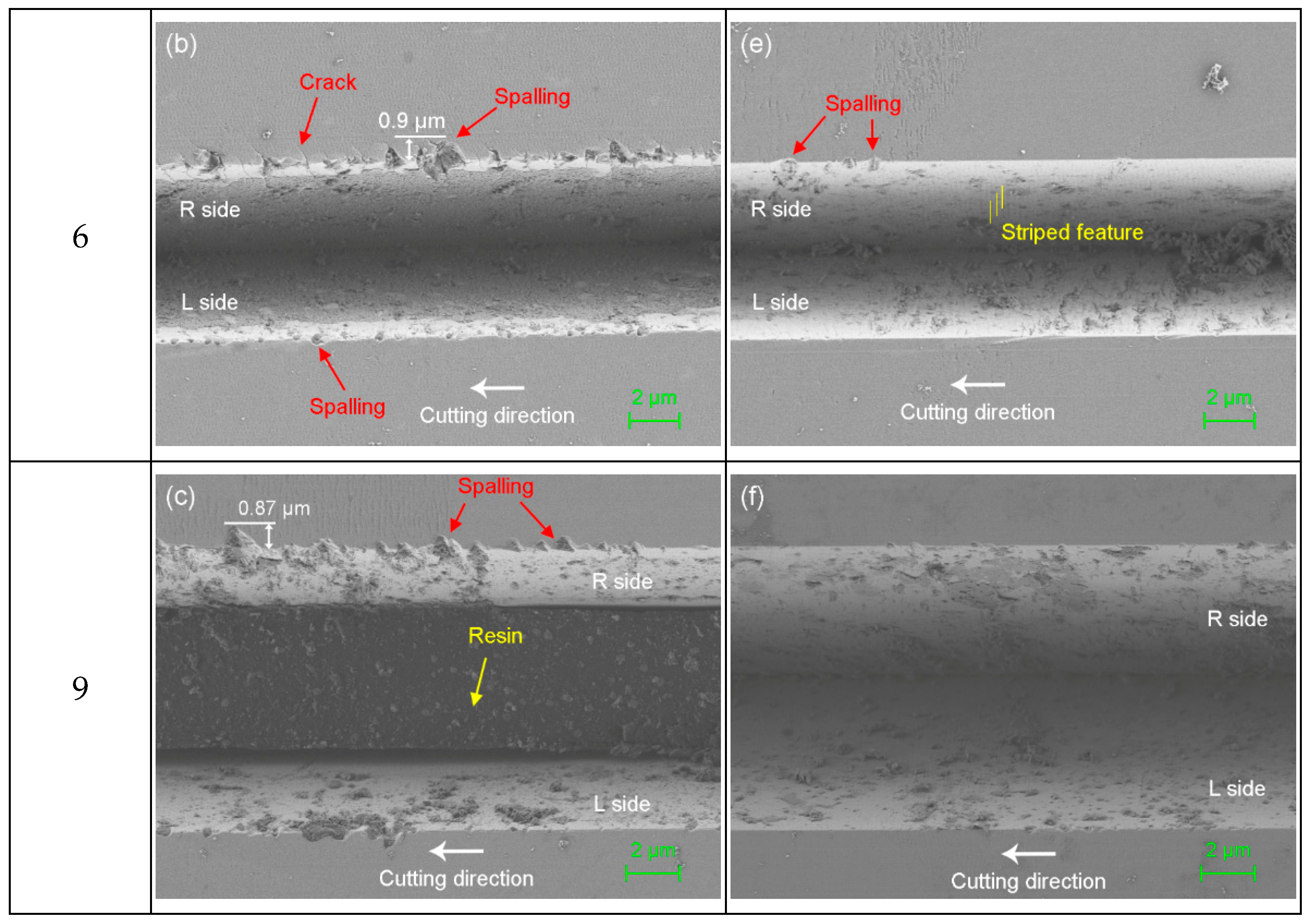
3.1. Effect of Resin Coating

Figure 4 shows the SEM images of typical morphologies of a V-shaped groove before removing the resin coating. It can be clearly observed from Figure 4a that the resin coating had been partially cut with the workpiece material and the remaining part was still adhered tightly to the workpiece surface after cutting. For further observing the surface quality of the machined workpiece and coating layer, as well as the features of workpiece-coating interface, a close-up view of the region marked by a red box in Figure 4a is presented in Figure 4b. On the workpiece surface, there were a lot of defects on the left (L) side of the groove, while an extremely smooth surface was created on the right (R) side of the groove. The difference in formation mechanisms of surface defects on the two sides will be discussed in Section 3.3.
On the other hand, the groove surface of the resin coating showed a homogeneous wave pattern, resulting a slightly rougher surface than the groove surface of the workpiece material. The rough groove surface of the resin coating is thought to be due to the viscoelastic properties of resin and low cutting speed. Since the cured photosensitive resin is a typical polymer material, the fracture strain is very low at room temperature. When the resin is cut at a low cutting speed, fractures occur due to the lack of heat-softening effect at a low cutting temperature [23,24]. Thus, the low fracture strain of the material may cause an unstable cutting process, resulting in a rough groove surface on the resin coating. The unstable cutting process caused by the resin coating, to some extent, may affect the groove surface quality of the workpiece material.
Figure 5 shows SEM images of the V-shaped grooves after removing the resin coating. For the grooves cut on the uncoated workpiece (Figure 5a–c), there were considerable spalling and cracks at the groove edge, although the extent of the damage to the L side and R side of the grooves were different. The maximum crack with a width of 0.9 μm was observed in the groove whose depth was 6 μm, as shown in Figure 5b. However, it seems that the extent of the defects at the groove edge is not related to the depth of groove. Similar defects can also be observed in the grooves with depth of 1 and 9 μm shown in Figure 5a,c, respectively. Compared with the edge of the groove, the surface of the grooves obtained a better surface quality, having less defects. This indicates that in the cutting of V-shaped grooves on soft-brittle materials, the edges of the grooves are easily fractured, even if the groove surfaces are removed in a ductile mode.
As for the grooves cut on the coated workpiece (Figure 5d–f), the spalling and cracks at the groove edge were effectively suppressed by the resin coating. The maximum width of the spalling was ~0.18 μm, which was much less than that on the uncoated workpiece. In addition, the surface of the grooves also became smoother. The improvement of surface integrity in V-shaped grooves by using resin coating was verified. In Figure 5e, it is worth noting that there are some striped features on the R side of the groove. This may be caused by the tool chatter that occurred during cutting the resin coating, which has a low fracture strain, as discussed in Figure 4b.
It should be pointed out that the cured resin is difficult to completely remove from the surface of the grooves even after cleaning. As shown in Figure 5, all the surfaces of grooves are adhered with resin, especially for the grooves which were cut on the uncoated workpiece (Figure 5c). This is because the grooves cut on the uncoated workpiece were coated by the photosensitive resin liquid during the preparation of coated workpiece (See Figure 3d). The resin flows into the grooves and is difficult to remove.

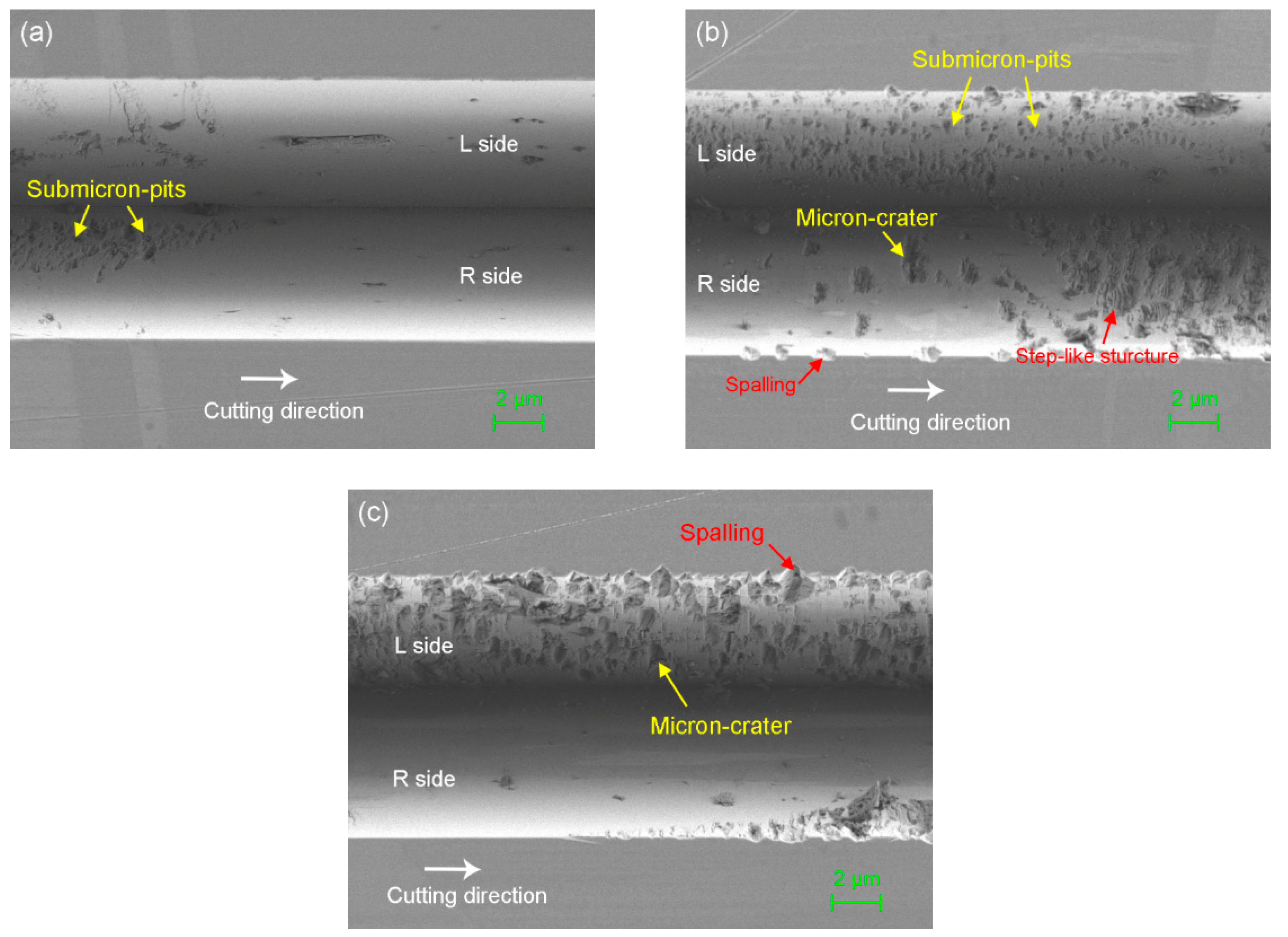
3.2. Effect of Tool Feed Rate

Figure 6 shows SEM images of V-shaped grooves cut on the resin coated workpiece at different feed rates fz. When the feed rate was 20 nm/rev, the edge of the groove was intact, although some defects were generated on the groove surface, as shown in Figure 6a. Those defects consisted of dense pits with a submicron scale. By increasing the feed rate to 40 nm/rev, craters with micron scale were observed on the R side surface of the groove, as shown in Figure 6b. In the micro craters, there is a stepped structure that is vertical to the cutting direction. Such stepped structures are the result of crack propagation, which happened along two cleavage planes that are perpendicular to each other [15,25]. However, on the L side surface of the groove, submicron-pits were observed, which were similar to the submicron-pits shown in Figure 6a. In addition, the spalling occurred at the edge of the groove when the surface defect was close to the edge, although the workpiece was coated with resin. At the feed rate of 60 nm/rev, as shown in Figure 6c, severe damage with micron-craters occurred on the L side surface of the groove and consequently caused the spalling at the edge of the groove. On the other hand, a better surface integrity was produced for the R side surface than the L side surface.
It can be concluded from the above results that when the feed rate is small, the defects that appear as the submicron-pits may occur on the groove surface. However, if the feed rate is increased, two kinds of surface defects, including submicron-pits and micron-craters, can be generated on the groove surface. The spalling at the edge of the groove is also likely to occur.
It is worth noting that even at the same feed rate and the same side of the groove, the grains of different crystal orientations show different surface features, as shown in Figure 6a. In Figure 6b,c, the L side surface and the R side surface of the groove within one grain also show different features. From these facts one may infer that the distribution and morphology of defects are closely related to the crystallographic orientation of the grains and the angle of groove surface. This issue will be discussed further in the next section.

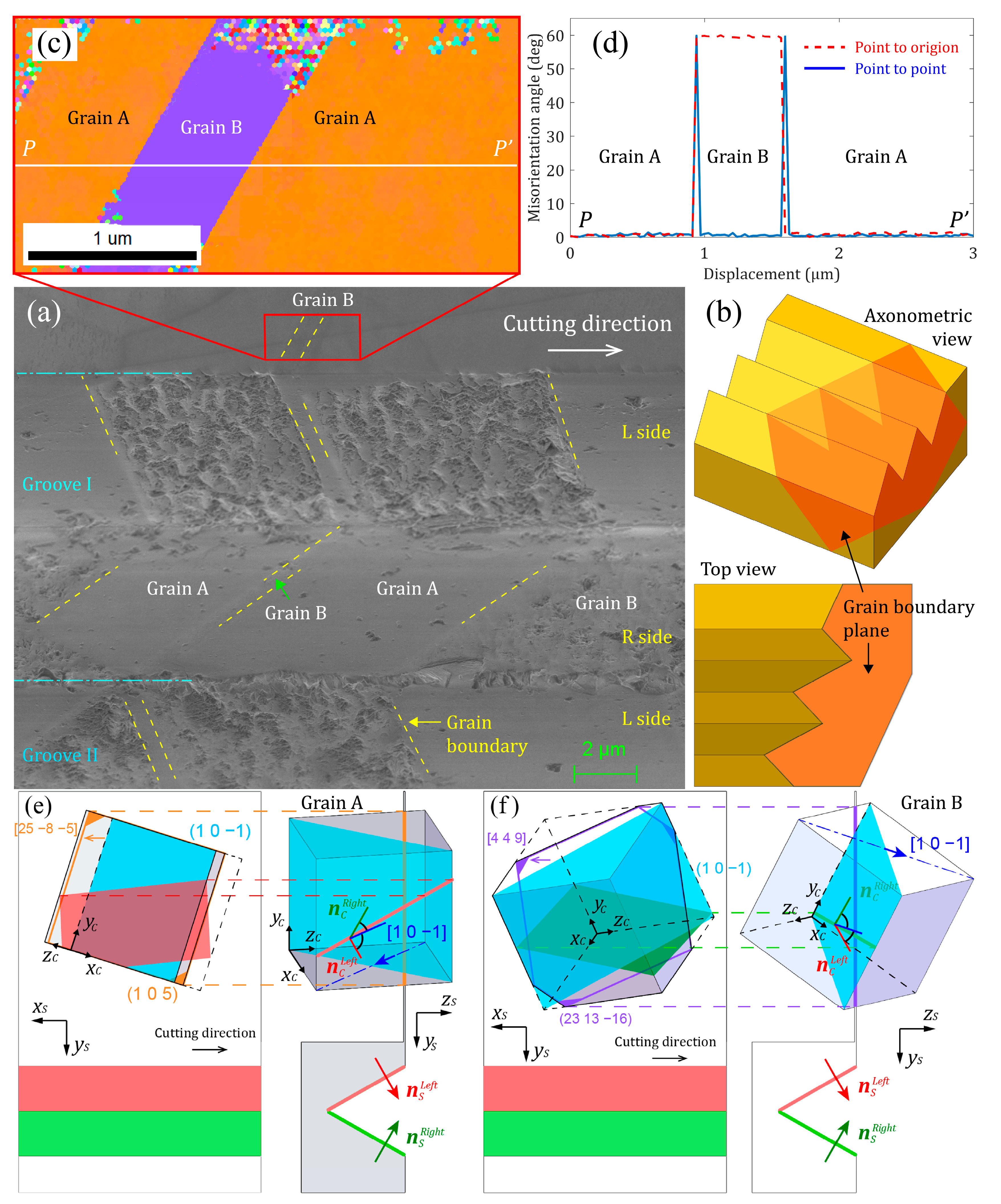
3.3. Formation Mechanism of Surface Defects

To investigate the formation mechanism of surface defects in the grooving process, a double-groove cutting experiment was conducted on the coated workpiece, as illustrated in Figure 7. Two grooves that are parallel and close to each other were cut at the same feed rate of 20 nm/rev. In this case, if the two grooves are through the same crystal grain, the features of the machined surface in the two grooves should be the same because the cutting conditions, including the grain orientation, cutting direction, and feed rate, for the two grooves are exactly the same. For example, as shown in Figure 7, in grain I, if the cracks appear on the R side of one groove, then cracks should also appear on the R side of the other groove. Similarly, in grain II, if the cracks appear on the L side of one groove, then cracks should also appear on the L side of the other groove.
Figure 8 shows the SEM image of a typical area covering the double grooves taken in Inlens Duo mode, which enables both Inlens SE (secondary electrons) and BSE (backscattered electrons) detectors for high-resolution topographical imaging of surfaces, to distinguish where the grain boundaries are. Along the direction perpendicular to the cutting direction, grain boundaries make up many zigzag shapes. It is supposed that each zigzag shape corresponds to a grain boundary, as schematically illustrated in Figure 8b. In addition, in grains with different crystallographic orientations, surface defects appear on different sides of the groove. In the same grain, the L side surface for both groove I and II exhibit the same feature. These results verify the hypothesis of Figure 7.
To further understand the dependence of defects formation mechanism on the grain orientation and the direction of side of groove, the crystallographic orientations of grains around the groove were characterized by EBSD analysis. It should be pointed out, however, that the groove surface cannot be directly detected by EBSD, owing to the working principle of EBSD that the target surface must be tilted by an angle of 70° to the orthogonal axis of the incident electron beam, and then EBSD detector receives the back scattered electron in an approximately horizontal direction [26]. Therefore, the crystallographic orientation of the workpiece surface next to the groove was characterized, as outlined by a red box in Figure 8a. The inverse pole figure (IPF) map of the corresponding region is presented in Figure 8b. It shows that there are two grains (A and B) with different crystallographic orientations. The orientations of the Gains A and B represented by Miller index are (1 0 5) [25-8-5] and (23 13-16) [4 4 9], respectively. The misorientation angle between grains A and B along Line PP’ was extracted from the IPF map, as plotted in Figure 8c. The misorientation angle between the two grains is 60°, which indicates that grains A and B are twin pairs having a coherent twin boundary around <111> [27]. From the above analysis, it can be inferred that the grains located within the SEM image area are dominated by grain A and grain B (Figure 8a).
As discussed in Section 3.2, the surface defects might be caused by the brittle fractures that occurred along cleavage planes. Therefore, it is necessary to find the relationship between the groove surface and the cleavage plane of the grain. The angle between the groove surface and grain’s cleavage plane can be calculated by:
θ = arccos n C l C | n C | | l C | ,
where nC is the normal vector of groove surface in crystal coordinate system (CCS). lC is the normal vector of grain’s cleavage plane in crystal coordinate system, which is {1 1 0} for ZnSe [28].
According to the geometry of the V-shaped tool, the normal vector of L side and R side surface of the groove in sample coordinate system (SCS) are n S L e f t = [ 0 , 3 2 , 1 2 ] and n S R i g h t = [ 0 , 3 2 , 1 2 ] , respectively, as illustrated in Figure 8e,f. The relationship between the crystal coordinate system and the sample coordinate system is given by:
n C = n S × g 1 ,
where g−1 is the inverse of rotation matrix g. The rotation matrix g can be expressed as:
g = [ u r h v s k w t l ]
[ r , s , t ] = [ u , v , w ] × [ h , k , l ]
Table 2 lists the angle between the most favorable cleavage plane and the groove surface in grains A and B, respectively. In grain A, the cleavage plane makes an angle of 86.5° to the L side surface of the groove, and 60.5° to the R side surface of the groove. Then, it was observed from Figure 8a that the surface defects occurred on the L side surface of the groove in grain A, rather than the R side surface. On the other hand, in grain B, the cleavage plane makes an angle of 44.8° to the L side surface of the groove, and 79.4° to the R side surface of the groove. As seen from Figure 8a, in grain B, the surface defects occurred on the R side surface of the groove, rather than the L side surface. These results reveal that if the groove surfaces are approximately perpendicular to the grain’s cleavage plane, surface defects are very easily to occur.
It is worth noting that in Figure 8a, on the R side surface of the groove I, the grain B with a narrow area (pointed by the green arrow) exhibits a crack-free surface, which is different from the grain B with a large area on its right side. In addition, by observing the SEM image shown in Figure 9, which was captured by HE-SE (high efficiency secondary electron) detector, narrow areas without cracks are found in the damaged surfaces in both grains A and B. These narrow areas always occur at the beginning of cutting of a new grain, as indicated by the green lines in Figure 9. This indicates that the grain boundary can block the stress spreading into the adjoining twin, and the cracks are initiated when the accumulated stress concentration exceeds a critical point. It is likewise observed from Figure 9 that in the groove I, the extent of damage on the L side surface of grain A is more severe than that on the R side surface of grain B. This might be attributed to the fact that the most favorable cleavage plane of grain A becomes almost perpendicular to the groove surface, while this is not the case for grain B.
Figure 10 shows schematic models of the formation mechanism of surface defects during the microgrooving process. When the tool feed rate is small, the undeformed chip thickness is also small, as shown in Figure 10a. Thus, the plowing effect is significant. The part of material below the segment point will not be separated from the workpiece [29]. Rather, the material is pressed by the tool and passes through below the tool tip, resulting in a plastic/elastic deformation layer. If this layer is formed in a grain in which the cleavage plane is vertical to the groove surface, tearing effects along the cleavage planes will occur during the elastic recovery of machined surface. Consequently, submicron-pits will generate on the groove surface.
When the feed rate is large, the undeformed chip thickness also becomes large, as shown in Figure 10b. Under this condition, a relatively high tensile stress will be generated in material along the cutting direction [25]. If such a stress state happens in a grain in which the cleavage plane is vertical to both cutting direction and groove surface, cracks can easily occur beneath the tool and propagate along both horizontal cleavage plane and vertical cleavage plane, which causes severe defects as micron-craters on the groove surface. However, if such a stress state happens in a grain in which the cleavage plane is not vertical to the groove surface, but crosses the groove surface at a large angle, cracks may still occur due to the high tensile stresses, resulting in the surface defects as submicron-pits.

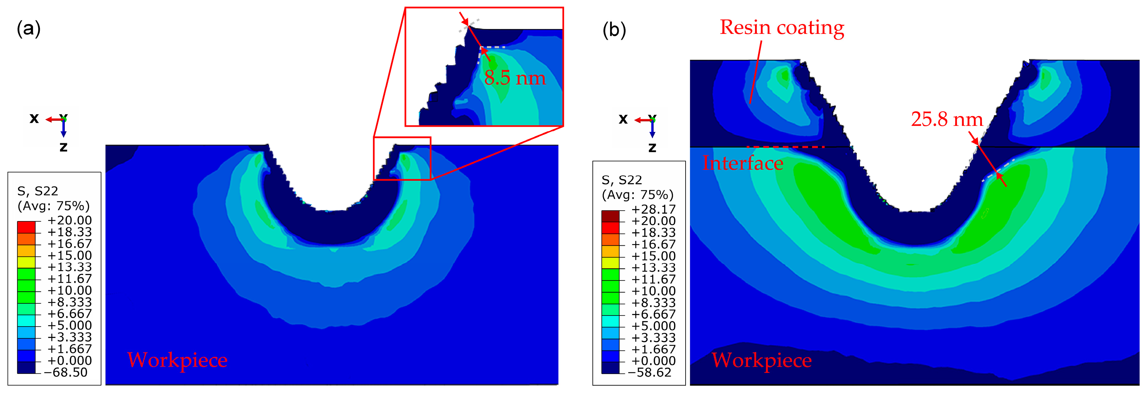
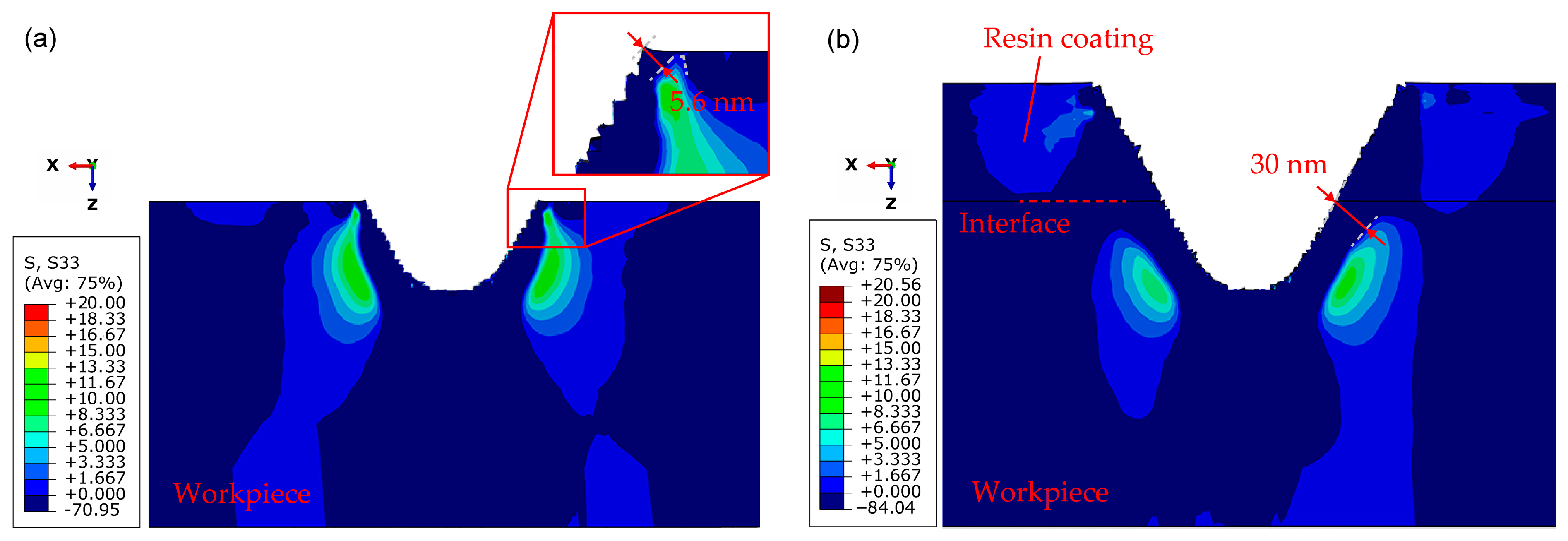
3.4. FEM Simulation of Stress Distribution

To clarify the reason that coating is effective in preventing initiation of cracks at the edge of grooves, the stress distribution of microgrooving process was investigated by finite element method (FEM) simulation using a commercially available software ABAQUS. Figure 11a shows the 3D simulation model of microgrooving process. The size of workpiece and coating were 500 × 800 × 220 nm and 500 × 800 × 80 nm, respectively, which were meshed by 106,400 and 159,600 eight-node linear brick elements (C3D8R). The cutting tool with an edge radius of 40 nm was meshed by quadratic tetrahedral elements (C3D10M) and was set as rigid body due to significantly high hardness of diamond tool compared to p-ZnSe. In the simulation configuration, as shown in Figure 11b, first the tool cut into the workpiece at a depth of cut of 30 nm. Then the tool fed 30 nm and cut the workpiece for the second time. The cutting speed was 0.2 m/s.
This simulation aimed at exploring the role of coating, thus the workpiece (p-ZnSe) was simplified as an isotropic material. The material properties of workpiece and coating in ABAQUS model are listed in Table 3. It should be noted that these parameters cannot correspond exactly to the real values. However, the simulation results can be considered as a guidance for understanding the effect of pre-coating on cutting of a soft-brittle material, because there is only one variable factor in this simulation, uncoated workpiece or coated workpiece. To model the adhesion of coating to workpiece, the surface interaction property between workpiece and coating was defined as a contact cohesive interface.
It has been widely accepted that the tensile stress is mainly responsible for the crack nucleation during cutting brittle materials. The tensile stresses along the cutting direction and the direction normal to the workpiece surface are responsible for the radial cracks and lateral cracks, respectively. Figure 12 shows a schematic diagram of crack generation in cutting groove on brittle materials. If the radial cracks and lateral cracks intersect with each other, the spalling of material is very likely to occur at the edge of the groove. Therefore, the tensile stresses along the cutting direction and the direction normal to the workpiece surface were examined after completing the simulation of the second cut. Although the simulated stress values in this study may be not quantitatively accurate, the results are adequate to achieve a qualitative comparison.
Figure 13a,b shows simulated distribution of the tensile stress along the cutting direction (σy) in uncoated workpiece and coated workpiece, respectively. It can be observed that a thin layer of material near the groove surface is under compressive stress, which is surrounded by a tensile stress field. This stress distribution is similar to that in an indentation test [32]. The pressure-induced densification and shear-induced plastic flow dominate the material in the small contact zone beneath the tool. After the tool passes, elastic recovery of the densified/deformed layer occurs, consequently the tensile stress tends to be enhanced along the boundary of the densified/deformed layer and the bulk, causing crack generation. In the uncoated workpiece, σy was concentrated closely to the edge of the groove and was featured by a sharp corner. However, in the coated workpiece, σy was distributed relatively farther from the edge of the groove and presented a smooth transition. That is, the compressive/tensile stress boundary near the edge of the groove was an arc without sharp edges and was farther away from the apex of the groove edge. As a result, radial cracks should be less likely to occur at the edge of the groove in the coated workpiece.
Figure 14a,b shows simulated distribution of the tensile stress along the direction normal to the workpiece surface (σz) in uncoated workpiece and coated workpiece, respectively. Similarly, in the uncoated workpiece, the σz was distributed very close to both the edge of the groove and the surface of the workpiece. The feature of the stress distribution pattern near the edge of the groove was likewise characterized as a sharp corner. However, in the coated workpiece, the σz was distributed relatively far from the edge of the groove and the surface of the workpiece. In addition, the feature of the stress distribution pattern near the edge of the groove presented a smooth transition. Therefore, lateral cracks should be less likely to occur at the edge of the groove in the coated workpiece. Based on the foregoing analysis, it can be concluded that the resin coating was able to make distribution of tensile stresses (both σy and σz) away from the edge of the groove and the workpiece surface, consequently suppressed brittle fractures at the edge of the groove.

4. Conclusions

Micro V-shaped grooves cutting experiments were conducted on polycrystalline zinc selenide. The effect of resin pre-coating of workpiece surface on the cutting behavior was investigated through experiments and FEM simulation. The mechanisms for surface defect formation were revealed. The major conclusions are summarized as follows:
(1)
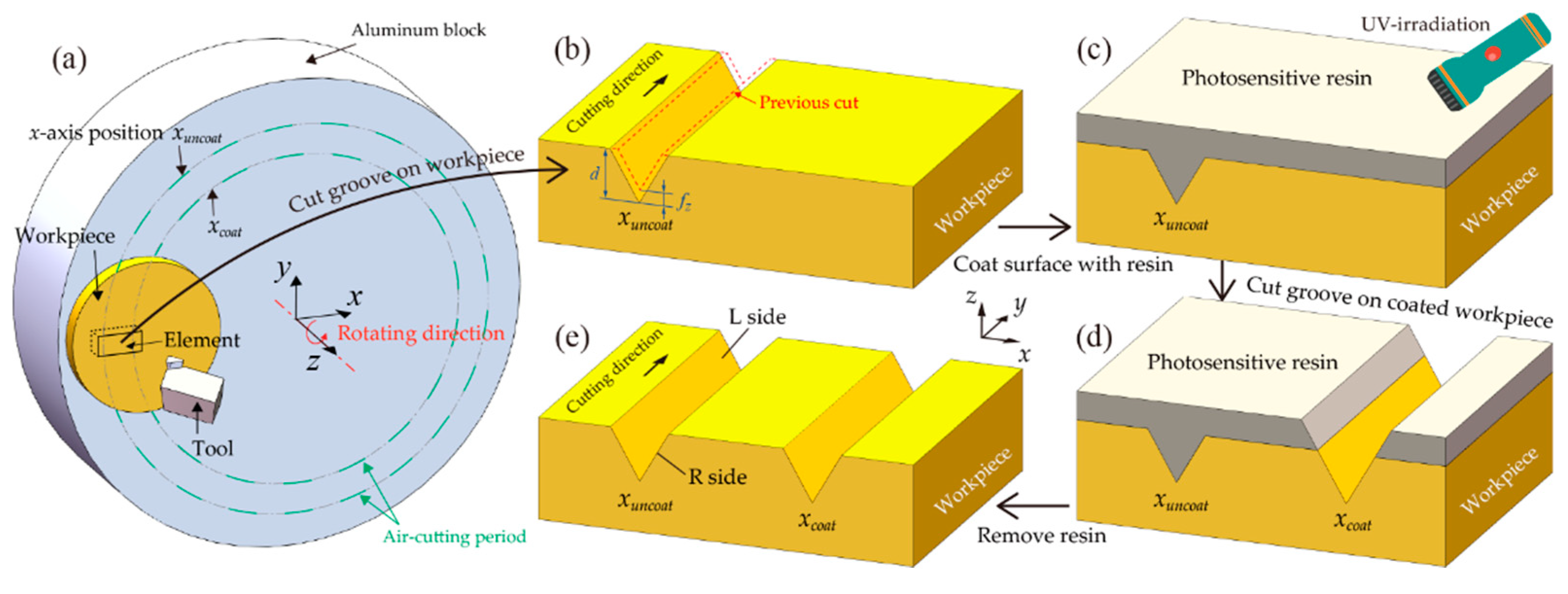
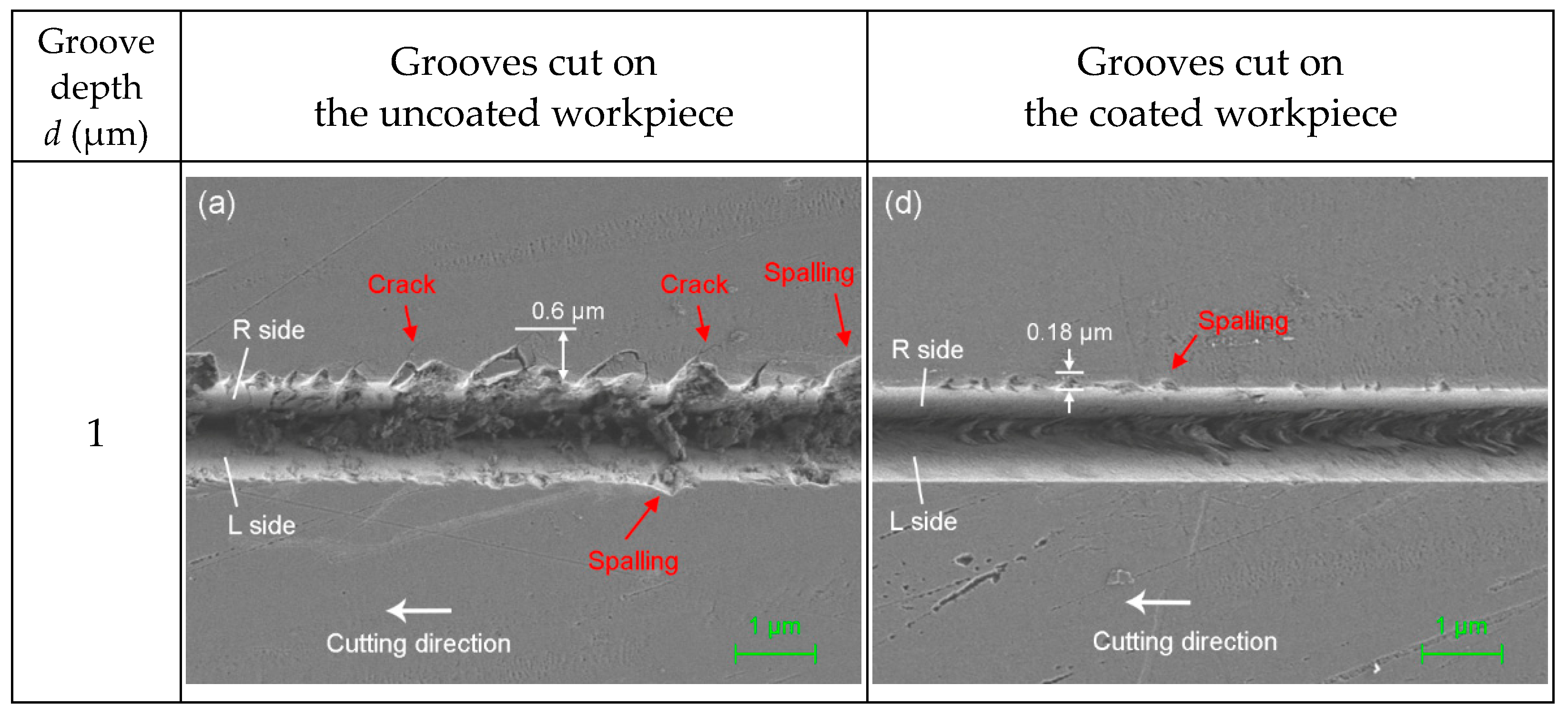
Application of a solidified coating layer of cured photosensitive resin on the workpiece surface before machining significantly suppressed brittle fractures at the edge of the groove, which solves the edge chipping problem in brittle materials grooving, although the side surfaces of the groove are unaffected.
(2)
When the tool feed rate is small (<20 nm/rev), submicron-pits were observed on the groove surface. Further increasing the feed rate, not only submicron-pits but also micron-craters were observed on the groove surface.
(3)
The two side surfaces of the V-shaped groove show distinctly different morphologies. The formation of defects is strongly dependent on the angle of groove surface with respect to cleavage plane of grain.
(4)
FEM simulation results demonstrated that the resin coating was able to make the tensile stresses along the cutting direction and the direction normal to the workpiece surface distributed away from the edge of the groove and the workpiece surface.
The results of this study demonstrate that workpiece pre-coating is an effective method to prevent crack formation at the groove edges when cutting micro V-shaped grooves on brittle polycrystalline materials. This finding provides a reference for surface integrity improvements in surface micro-structuring of such materials. As the coating material, photosensitive resin has been attempted and its effectiveness demonstrated. However, resin tightly adheres to the workpiece surface, which is difficult to completely remove from the surface of the grooves even after cleaning. In addition, the low fracture strain of cured resin may make the cutting process unstable. Therefore, other coating materials will be attempted in the future to achieve both good machinability and strong adhesion property with the workpiece.

Author Contributions

W.H.: Data curation, investigation, writing—original draft. J.Y.: Conceptualization, methodology, supervision, writing—review and editing. All authors have read and agreed to the published version of the manuscript.

Funding

This work has been partially supported by KLL Program Research Grant of Keio University.

Institutional Review Board Statement

Not applicable.

Informed Consent Statement

Not applicable.

Acknowledgments

Thanks are extended to Kawori Tanaka of Central Testing Center, Keio University for her assistance of SEM and EBSD observations.

Conflicts of Interest

The authors declare no conflict of interest.

References

  1. Liu, Q.; Liao, Z.; Axinte, D. Temperature effect on the material removal mechanism of soft-brittle crystals at nano/micron scale. Int. J. Mach. Tools Manuf. 2020, 159, 103620. [Google Scholar] [CrossRef]
  2. Yan, J.; Tamaki, J.I.; Syoji, K.; Kuriyagawa, T. Single-point diamond turning of CaF2 for nanometric surface. Int. J. Adv. Manuf. Technol. 2004, 24, 640–646. [Google Scholar] [CrossRef]
  3. Fang, F.Z.; Venkatesh, V.C.; Zhang, G.X. Diamond turning of soft semiconductors to obtain nanometric mirror surfaces. Int. J. Adv. Manuf. Technol. 2002, 19, 637–641. [Google Scholar] [CrossRef] [Green Version]
  4. Zhang, Z.; Yan, J.; Kuriyagawa, T. Manufacturing technologies toward extreme precision. Int. J. Extrem. Manuf. 2019, 1, 22001. [Google Scholar] [CrossRef] [Green Version]
  5. Mukaida, M.; Yan, J. Ductile machining of single-crystal silicon for microlens arrays by ultraprecision diamond turning using a slow tool servo. Int. J. Mach. Tools Manuf. 2017, 115, 2–14. [Google Scholar] [CrossRef]
  6. Zhang, L.; Zhou, L.; Zhou, W.; Zhang, S.; Yi, A.Y. Design, fabrication and testing of a compact large-field-of-view infrared compound eye imaging system by precision glass molding. Precis. Eng. 2020, 66, 87–98. [Google Scholar] [CrossRef]
  7. Zhang, S.; Zhou, Y.; Zhang, H.; Xiong, Z.; To, S. Advances in ultra-precision machining of micro-structured functional surfaces and their typical applications. Int. J. Mach. Tools Manuf. 2019, 142, 16–41. [Google Scholar] [CrossRef]
  8. Brinksmeier, E.; Karpuschewski, B.; Yan, J.; Schönemann, L. Manufacturing of multiscale structured surfaces. CIRP Ann. 2020, 69, 717–739. [Google Scholar] [CrossRef]
  9. Tong, Z.; Zhong, W.; To, S.; Zeng, W. Fast-tool-servo micro-grooving freeform surfaces with embedded metrology. CIRP Ann. 2020, 69, 505–508. [Google Scholar] [CrossRef]
  10. Guo, J.; Zhang, J.; Pan, Y.; Kang, R.; Namba, Y.; Shore, P.; Yue, X.; Wang, B.; Guo, D. A critical review on the chemical wear and wear suppression of diamond tools in diamond cutting of ferrous metals. Int. J. Extrem. Manuf. 2020, 2, 12001. [Google Scholar]
  11. Mukaida, M.; Yan, J. Fabrication of hexagonal microlens arrays on single-crystal silicon using the tool-servo driven segment turning method. Micromachines 2017, 8, 323. [Google Scholar] [CrossRef] [Green Version]
  12. Zhu, Z.; Tong, Z.; To, S.; Jiang, X. Tuned diamond turning of micro-structured surfaces on brittle materials for the improvement of machining efficiency. CIRP Ann. 2019, 68, 559–562. [Google Scholar] [CrossRef]
  13. Jasinevicius, R.G.; Duduch, J.G.; Cirino, G.A.; Pizani, P.S. Diamond turning of small Fresnel lens array in single crystal InSb. J. Micromech. Microeng. 2013, 23, 55025. [Google Scholar] [CrossRef]
  14. Yan, J.; Maekawa, K.; Tamaki, J.; Kuriyagawa, T. Micro grooving on single-crystal germanium for infrared Fresnel lenses. J. Micromech. Microeng. 2005, 15, 1925–1931. [Google Scholar] [CrossRef]
  15. Huang, W.; Yan, J. Surface formation mechanism in ultraprecision diamond turning of coarse-grained polycrystalline ZnSe. Int. J. Mach. Tools Manuf. 2020, 153, 103554. [Google Scholar] [CrossRef]
  16. Blake, P.N.; Scattergood, R.O. Ductile-regime machining of germanium and silicon. J. Am. Ceram. Soc. 1990, 73, 949–957. [Google Scholar] [CrossRef]
  17. Yan, J.; Oowada, T.; Zhou, T.; Kuriyagawa, T. Precision machining of microstructures on electroless-plated NiP surface for molding glass components. J. Mater. Process. Technol. 2009, 209, 4802–4808. [Google Scholar] [CrossRef]
  18. Guo, J.; Zhang, J.; Wang, H.; Liu, K.; Kumar, A.S. Surface quality characterisation of diamond cut V-groove structures made of rapidly solidified aluminium RSA-905. Precis. Eng. 2018, 53, 120–133. [Google Scholar] [CrossRef]
  19. Heidari, M.; Yan, J. Ultraprecision surface flattening of porous silicon by diamond turning. Precis. Eng. 2017, 49, 262–277. [Google Scholar] [CrossRef]
  20. Lee, Y.J.; Chong, J.Y.; Chaudhari, A.; Wang, H. Enhancing ductile-mode cutting of calcium fluoride single crystals with solidified coating. Int. J. Precis. Eng. Manuf. Green Technol. 2019, 7, 1019–1029. [Google Scholar] [CrossRef]
  21. Kalkhoran, S.N.A.; Vahdati, M.; Zhang, Z.; Yan, J. Influence of Wax Lubrication on Cutting Performance of Single-Crystal Silicon in Ultraprecision Microgrooving. Int. J. Precis. Eng. Manuf. Green Technol. 2020. [Google Scholar] [CrossRef]
  22. Huang, W.; Yan, J. Chip-free surface patterning of toxic brittle polycrystalline materials through micro/nanoscale burnishing. Int. J. Mach. Tools Manuf. 2021, 162, 103688. [Google Scholar] [CrossRef]
  23. Carr, J.W.; Feger, C. Ultraprecision machining of polymers. Precis. Eng. 1993, 15, 221–237. [Google Scholar] [CrossRef]
  24. Yan, J. Ultraprecision cutting of photoresist/gold composite microstructures. CIRP Ann. 2011, 60, 133–136. [Google Scholar] [CrossRef]
  25. Yan, J.; Syoji, K.; Kuriyagawa, T.; Suzuki, H. Ductile regime turning at large tool feed. J. Mater. Process. Technol. 2002, 121, 363–372. [Google Scholar] [CrossRef]
  26. Sun, H.; Adhyaksa, G.W.P.; Garnett, E.C. The Application of Electron Backscatter Diffraction on Halide Perovskite Materials. Adv. Energy Mater. 2020, 10, 2000364. [Google Scholar] [CrossRef]
  27. Jung, J.; Yoon, J.I.; Kim, J.G.; Latypov, M.I.; Kim, J.Y.; Kim, H.S. Continuum understanding of twin formation near grain boundaries of FCC metals with low stacking fault energy. Npj Comput. Mater. 2017, 3, 21. [Google Scholar] [CrossRef] [Green Version]
  28. Sun, Y.; Sun, Z.; Gao, S.; Cheng, H.; Liu, Q.; Piao, J.; Yao, T.; Wu, C.; Hu, S.; Wei, S.; et al. Fabrication of flexible and freestanding zinc chalcogenide single layers. Nat. Commun. 2012, 3, 1057. [Google Scholar] [CrossRef] [PubMed]
  29. Huang, W.; Yu, D.; Zhang, M.; Cao, Q.; Yao, J. Predictive cutting force model for ductile-regime machining of brittle materials. Int. J. Adv. Manuf. Technol. 2018, 98, 781–790. [Google Scholar] [CrossRef]
  30. Material Properties of ZnSe. Available online: https://www.pveducation.org/pvcdrom/materials/znse (accessed on 20 December 2020).
  31. Jiang, C.; Zhao, G. A Preliminary Study of 3D Printing on Rock Mechanics. Rock Mech. Rock Eng. 2015, 48, 1041–1050. [Google Scholar] [CrossRef]
  32. Lawn, B.; Wilshaw, R. Indentation fracture: Principles and applications. J. Mater. Sci. 1975, 10, 1049–1081. [Google Scholar] [CrossRef]
Figure 1. Machining models of (a) flat surface cutting using a round-nosed tool; (b) V-shaped groove cutting using a V-shaped tool.
Jmmp 05 00017 g001
Figure 2. (a) Experimental setup for off-axis diamond cutting of micro V-shaped grooves; (b) SEM image of the diamond tool with an extremely sharpened tool tip.
Jmmp 05 00017 g002
Figure 3. Schematic diagram of the experimental procedure: (a) Off-axis cutting; (b) cutting grooves on uncoated workpiece; (c) coating workpiece surface with photosensitive resin; (d) cutting grooves on coated workpiece; and (e) removing the photosensitive resin. The workpiece shown in Figure 3bd is a small-area extraction from Figure 3a. For simplicity, the grooves in Figure 3bd are approximated to be straight, as the curvature is extremely small in such a small area.
Jmmp 05 00017 g003
Figure 4. SEM images of the V-shaped groove before removing the resin coating (a) general view; (b) close-up view. (Cutting parameters: fz = 10 nm/rev, and d = 9 μm).
Jmmp 05 00017 g004
Figure 5. SEM images of the V-shaped grooves after removing the resin coating (all grooves were cut at fz = 10 nm/rev).
Jmmp 05 00017 g005aJmmp 05 00017 g005b
Figure 6. SEM images of V-shaped grooves cut at different feed rates: (a) 20 nm/rev; (b) 40 nm/rev; (c) 60 nm/rev.
Jmmp 05 00017 g006
Figure 7. Schematic diagram of double-groove cutting experiment.
Jmmp 05 00017 g007
Figure 8. (a) SEM image of a typical area in the double groove taken in Inlens Duo mode; (b) schematic drawings of the grain boundary plane which corresponds to the grain boundary in SEM image; (c) IPF map of the region outlined by red box in SEM image; (d) misorientation angle profile along Line PP’ indicated in IPF map. Schematic diagram of the spatial relationship between V-shaped groove and (e) grain A and (f) grain B.
Jmmp 05 00017 g008
Figure 9. SEM image of the same region as Figure 8a by HE-SE detector.
Jmmp 05 00017 g009
Figure 10. Schematic model for (a) formation of submicron-pits; (b) formation of micron-crater.
Jmmp 05 00017 g010
Figure 11. (a) 3D simulation model of microgrooving process; (b) schematic of simulation configuration showing two paths of cutting tool.
Jmmp 05 00017 g011
Figure 12. Schematic diagram of crack generation in cutting groove on brittle materials.
Jmmp 05 00017 g012
Figure 13. FEM-simulated tensile stress along cutting direction (y-axis direction) in: (a) Uncoated workpiece; (b) coated workpiece.
Jmmp 05 00017 g013
Figure 14. FEM-simulated tensile stress along the direction normal to the workpiece surface (z-axis direction) in: (a) Uncoated workpiece; (b) coated workpiece.
Jmmp 05 00017 g014
Table 1. Machining parameters for micro V-shaped grooves cutting experiment.
Exp. No.ConditionSpindle Rotation Rate S (rpm)Groove Depth d (μm)Feed Rate fz (nm/rev)
1–3Uncoated workpiece501, 6, 910
4–6Coated workpiece1, 6, 910
7–9Coated workpiece920, 40, 60
Table 2. Calculated angle between the most favorable cleavage plane and the surface of groove.
Grain No.Cleavage PlaneGroove SurfaceAngle (Deg.)
DirectionNormal Vector in SCSNormal Vector in CCS
A 1(1 0 −1)Left [ 0 , 3 / 2 , 1 / 2 ] [ 0.3523 , 0.8263 , 0.4394 ] 86.5
Right [ 0 , 3 / 2 , 1 / 2 ] [ 0.1562 , 0.8263 , 0.5411 ] 60.5
B 2Left [ 0 , 3 / 2 , 1 / 2 ] [ 0.8497 , 0.5044 , 0.1535 ] 44.8
Right [ 0 , 3 / 2 , 1 / 2 ] [ 0.1051 , 0.9252 , 0.3645 ] 79.4
1 Miller index of grain A is (1 0 5) [25 −8 −5]. 2 Miller index of grain B is (23 13 −16) [4 4 9].
Table 3. Material properties of p-ZnSe and resin in ABAQUS model [30,31].
Materialp-ZnSeResin
Young’s modulus E (GPa)70.32.7
Shear modulus G (GPa)28.92.98
Critical tensile strength σc (MPa)41.335.5
Critical shear strength τc (MPa)57.820.2
Poisson’s ratio ν0.280.2
Density ρ (g/cm3)5.2661.1
Publisher’s Note: MDPI stays neutral with regard to jurisdictional claims in published maps and institutional affiliations.

