Article

Vanadium Dioxide–Iridium Composite Development: Specific Near Infrared Surface Plasmon Resonance

by
Adrian Ionut Bercea
*,
Corinne Champeaux
,
Catalin Daniel Constantinescu
and
Frédéric Dumas-Bouchiat
*
Université de Limoges, CNRS, IRCER, UMR 7315, F-87000 Limoges, France
*
Authors to whom correspondence should be addressed.
J. Compos. Sci. 2021, 5(7), 193; https://0-doi-org.brum.beds.ac.uk/10.3390/jcs5070193
Submission received: 18 June 2021 / Revised: 9 July 2021 / Accepted: 14 July 2021 / Published: 20 July 2021
(This article belongs to the Special Issue Feature Papers in Journal of Composites Science in 2021)

Abstract

:
This work serves as a roadmap for the development of a Vanadium dioxide (VO2)–Iridium composite based on the self-assembly of closely packed colloidal polystyrene microspheres (P-spheres) coupled with a Pulsed Laser Deposition (PLD) process. The self-assembly of a monolayer of PS is performed on an Al2O3-c substrate, using an adapted Langmuir–Blodgett (LB) process. Then, on the substrate covered with P-spheres, a 50-nanometer Iridium layer is deposited by PLD. The Iridium deposition is followed by the removal of PS with acetone, revealing an array of triangular shaped metallic elements formed on the underlaying substrate. In a last deposition step, 50-, 100- and 200-nanometer thin films of VO2 are deposited by PLD on top of the substrates covered with the Iridium quasi-triangles, forming a composite. Adapting the size of the P-spheres leads to control of both the size of the Iridium micro-triangle and, consequently, the optical transmittance of the composite. Owing to their shape and size the Iridium micro-triangles exhibit localized surface plasmon resonance (LSPR) characterized by a selective absorption of light. Due to the temperature dependent properties of VO2, the LSPR properties of the composite can be changeable and tunable.

1. Introduction

Due to their ability to bring together and combine properties of different materials, composites find usage in a variety of applications. Composites are the future of materials and their field of applications, ranging from the development of hard–soft composite magnets [1] to the advances in light manipulation using composite nanostructures [2,3] or to nanocomposites based supercapacitors [4], is only expected to increase with time. Here, we propose the development of a composite based on the following two complementary materials: a noble metal (Iridium) that constitutes a sub-micro element of the composite and smart oxide matrix (Vanadium dioxide VO2) for infrared surface plasmon resonance-based applications. The Vanadium dioxide–Iridium composite development is made possible by using the self-assembly of closely packed colloidal polystyrene microspheres (P-spheres) on an Al2O3-c substrate and a Pulsed Laser Deposition (PLD) process. The PS serve as templates/masks for the Ir microtriangle deposition using PLD. In a second step, VO2 thin films are deposited on the substrate decorated with the Ir microtriangles, thus forming the composite. When the Iridium triangles are excited by electromagnetic radiation, the metallic elements show collective oscillations of their conduction electrons known as localized surface plasmon resonances (LSPR). The wavelength position of the LSPR peak depends on the size, shape and dielectric properties of the metal elements and is affected by the surrounding environment. The choice of vanadium dioxide as a covering matrix is based on its “smart” properties. With a notable metal-insulator transition (MIT) at a critical temperature of 68 °C, VO2 has become, in the last few decades, since the pioneer Morin’s work in 1959 [5], a material of great interest because of its promising strengths to investigate applications as new further thermochromic, electronic, thermal and optic switching devices [6,7,8]. Indeed, the VO2 MIT is characterized by rapid (10−9–10−12 ns) [9], huge and sharp changes in physical properties such as optical absorption, dielectric function and electrical and thermal conductivity [10]. However, obtaining a pure VO2 phase is very challenging due to its narrow range of thermodynamic stability among some seventeen vanadium oxides, explaining the diverse chemical or physical techniques studied to grow VO2 thin film [11,12,13,14]. Pulsed laser deposition is one of the most interesting processes to deposit pure VO2 thin films, by controlling several deposition parameters such as temperature, pressure and fluence [15,16]. Moreover, due to a very high melting temperature, i.e., 2466 °C, it is also challenging to deposit thin Iridium films [17,18]. Using a highly powerful nano-second pulsed laser (108–109 GW), the ablation of all the elements is possible, even for the most refractory. PLD is then also a convenient process to deposit Ir metallic films.
In the literature, VO2-based composites for plasmonic applications often involve gold or silver inclusions as the metal component [19,20,21]. VO2 deposition requires the substrate to be heated up to about 500 °C. This necessary temperature induces metal deformations, metallic melting and the metal de-wetting process, and consequently, gold or silver sketches or nanoparticles are affected, changing their shape and size, making it difficult to the understand and control the composite properties. In particular, the effects on the plasmonic characteristics of the composite of the dielectric environment are coupled with the contribution of the shape change of the nanoparticles. The high melting temperature of Iridium makes it an ideal candidate for isolating and understanding the contribution of such a complex dielectric environment (VO2) to the plasmonic properties of the composite. In this context, the aim of our work is to precisely quantify the influence of VO2 MIT characteristics onto the nanocomposite plasmonic behavior and to combine the metallic plasmonic properties with the dielectric tunability of VO2, resulting in a system that is able to tune the light transmittance in the InfraRed range.

2. Materials and Methods

The VO2–Ir composites are manufactured using a combination of the two processes (Langmuir–Blodgett colloidal lithography and Pulsed Laser Deposition) presented in Figure 1. First, polystyrene microspheres (P-spheres) are assembled in the form of a monolayer on a substrate, using a derivative-Langmuir–Blodgett colloidal lithography process (KSV Nima << Langmuir–Blodgett Deposition Through Medium, KN 2002 >>). The LB principle consists of the transfer of a one-molecule thick layer (Langmuir monolayer) spread at the air/sub-phase (in general water) interface onto a receiving substrate. On the basis of this classical process, the LB principle has been adapted for microsphere colloidal lithography. The role of the classical amphiphilic molecules is played by microspheres of polystyrene functionalized with a steric acid group, e.g., C18–triethoxy (octadecyl) silane [22]. Here, the colloidal lithography experiments are performed using P-spheres with diameters of 2 and 3 µm, commercially available at Microparticles GmbH® and Micro Partikeltechnologie GmbH®. The P-spheres are commercialized already functionalized with C18 and sold as a water suspension of 10 mL, 50 mg/mL. In a single colloidal lithography experiment, 7500 µL of ethanol are added to 2500 µL of P-spheres suspension and then the mixture is transferred on the surface of 230 mL of distilled water that acts as a sub-phase. The ethanol adjusts the surface tension of water and controls the interaction between the P-spheres, thereby enabling the formation of a P-spheres monolayer on the surface of the sub-phase. Then, the resulting P-spheres monolayer is further compressed to a surface tension of around 40 mN/m by using the barriers of the LB system and transferred onto an Al2O3-c substrate.
In a second experimental step, the Al2O3-c substrates decorated with P-spheres are covered by Iridium thin films using the PLD process. The 50-nanometer thin films of Iridium are deposited using a pulsed KrF laser (TUI ThinFilmStar100) working at a wavelength of 248 nm at 10 Hz and a fluence of 2–3 J/cm2. The deposition of Iridium is carried out in a vacuum (1 × 10⁻⁷ mbar) and at room temperature (~25 °C). After the Iridium deposition, the P-spheres are removed with acetone, revealing a periodic and organized array of microtriangles. The resulting Iridium sketch is further covered with a thin film of Vanadium dioxide deposited using the PLD system, with identical pulsed laser and fluence in a reactive oxygen environment at a pressure of 2.2 × 10⁻² mbar and a deposition temperature of 500 °C. Different composites are made using vanadium dioxide with three thicknesses of 50, 100 and 200 nm, respectively. After the second deposition process, a composite consisting of Iridium microtriangles embedded in Vanadium dioxide is achieved. The optical characteristics of the composites are determined by transmittance measurements performed using a Fourier Transform InfraRed Spectroscopy (FTIR) (ThermoFisher-Nicolet 6700) system for the 1.5 to 5.5 µm optical wavelength range. The structural properties of the VO2–Ir microtriangles composites have been investigated using X-ray diffraction (XRD) in θ-2θ geometry (Bruker diffractometer, model “D8 Advance”, CuKα x-ray source, λ = 0.154 nm) equipped with a focusing Kα1 mono filter and detector (LynxEye, model “A17-B60”). The ImageJ and OriginPro 2015 software are used for data processing.

3. Results and Discussions

In this article, experiments realized with 2 or 3 µm P-spheres give the same type of composites, the same behavior and similar results except for the geometrical considerations. The results obtained using 2 or 3 µm P-spheres will then be representative of the general composite characteristics and will be alternatively used.

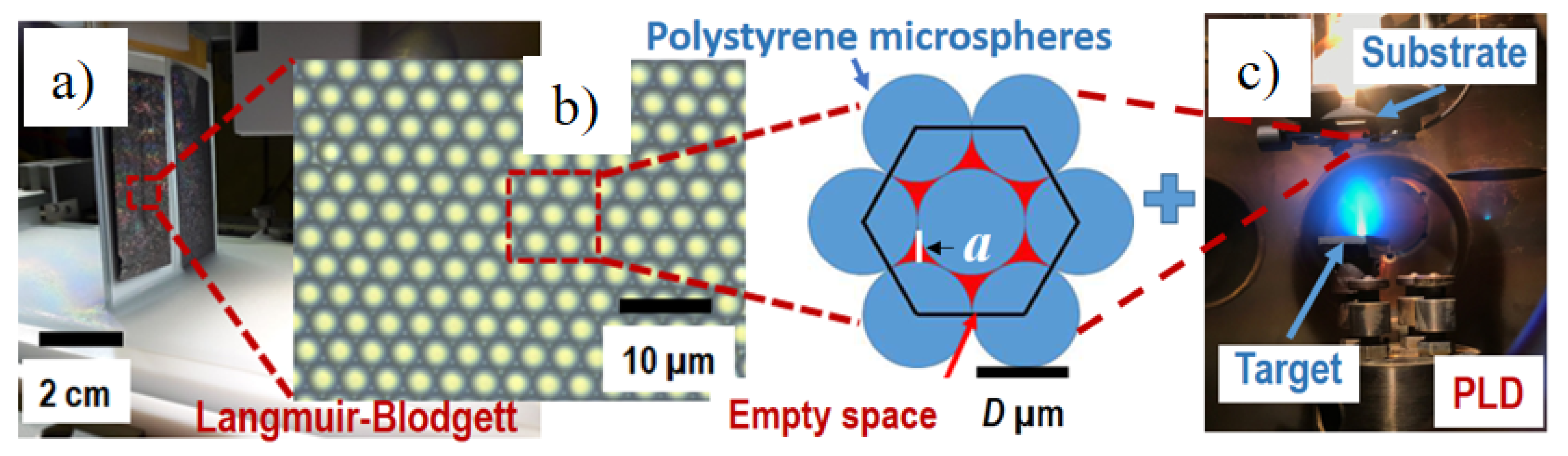
3.1. Colloidal Lithography: 2D Arrangement of the Polystyrene Microspheres (P-Spheres) and Optimization Processes

In Langmuir–Blodgett colloidal lithography, the most common close packed P-spheres arrangements resemble a 2D crystal with a hexagonal close packed structure. In practice, the formation of the monolayer of P-spheres with a perfect 2D crystal structure is controlled by the optimization of the Langmuir–Blodgett procedure itself coupled with the intrinsic characteristics (polydispersity, sphericity, etc.) of the P-spheres. Here, the P-spheres are commercially provided by Microparticles GmbH® and Micro Partikeltechnologie GmbH®. Thereby, all the improvements of the 2D structure are only made by the optimization of the process. In LB, the P-spheres monolayer formation is driven by the balance of the different forces, (attractive or repulsive). Forces such as Van der Waals interaction, electrostatic interaction, steric effect and capillary forces govern the interaction and arrangement in crystalline domains of P-spheres [23]. The capillary forces depend on the sphericity or on the “irregular contact line” between the individual P-spheres [24]. However, the Van der Waals interaction, electrostatic interaction and steric depend on the working temperature of the LB process [23]. This well-known phenomenon is clearly revealed in Figure 2. The quality of the arrangement of the P-spheres depends on the temperature. At 20 °C (Figure 2a), the P-spheres monolayer partially collapses, resulting in the deposition of additional P-spheres on top of the main monolayer. At 30 °C (Figure 2c), the P-sphere monolayer also partially collapses in a similar manner to Figure 2a. When the temperature is set to 25 °C (Figure 2b), the best arrangements are obtained and the number of additional P-spheres on top of the main monolayer reaches a minimum.
Besides the presence of an additional P-sphere on top of the main monolayer, the size of the individual crystalline domains is also of great interest. Ideally, all the P-spheres should arrange in a single crystallin domain on the substrate, but in practice the P-spheres monolayer is composed of multiple domains resembling a 2D poly crystalline entity. The quality of the P-spheres arrangement can be assessed through the generation of a Fast Fourier transform (FFT) [25]. The results of the FFT procedure are presented in inserts of Figure 2. A ring in a reciprocal space (after FFT calculation) is proof of the presence of a constant characteristic distance in all directions in the 2D space. This is the case for P-spheres arrangements at 20 °C (see Figure 2a). If specific directions are favorized (increasing the quality of the arrangements), then discrete points appear symmetrical to the center in the reciprocal space (see Figure 2b,c). The diameter or the distance between two points are inversely proportional to the characteristic length. The FFT calculation shows that the quality and size of the individual 2D crystalline domains increase versus the temperature. There is, however, a tradeoff between increasing the size of the individual 2D domains and the presence of additional P-spheres on top of the main monolayer. Considering these two aspects, domain size vs. additional P-spheres, 25 °C (see Figure 2) constitutes the optimal P-spheres deposition temperature for the presented system. In addition to the temperature, the substrate nature can modify the surface tension and affect the sphere organization. To emphasis this effect, experiments were conducted with two other substrates, a Borosilicate glass (BK7) and a silicon (Si) wafer, in the same deposition process. At the three substrate surfaces, P-spheres depositions present identical characteristics for the optimized temperature of 25 °C (data not shown here).

3.2. VO2–Ir Microtriangles Composite Development

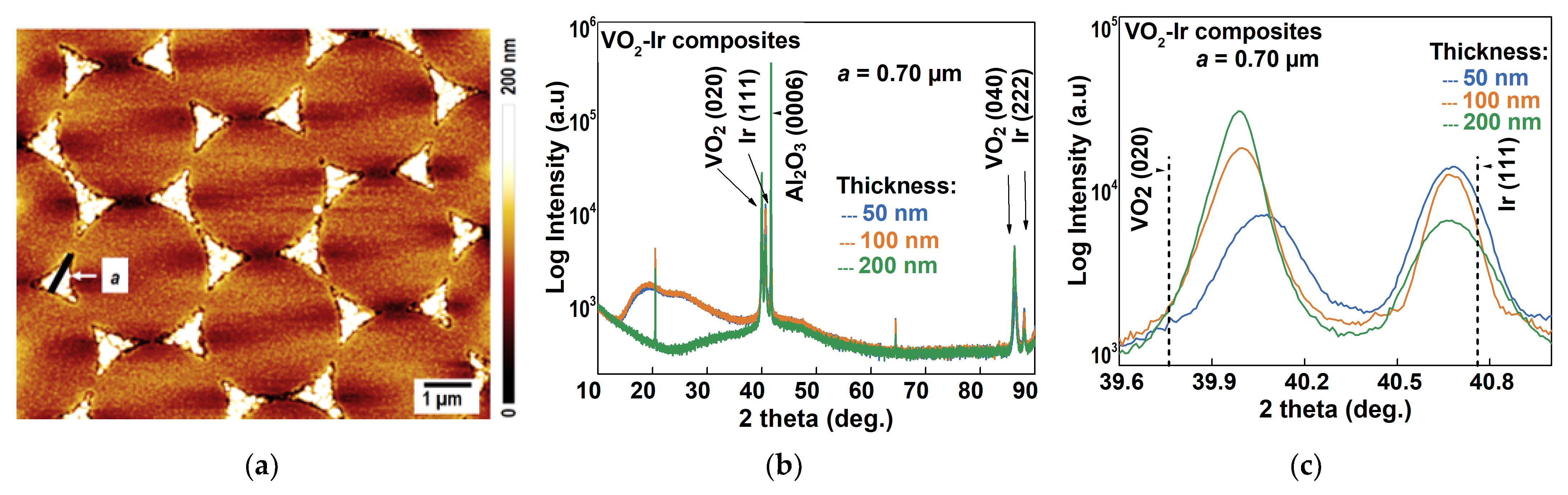
3.2.1. VO2–Ir Microtriangles Composite Development and Structural Characteristics

In the 2D hexagonal arrangement, the maximum coverage rate of the substrate, τsphere_covering, by the P-spheres, is defined by Equation (1).
τsphere_covering = Smichosphere/Stotal = Areadisk/Areahexagon = π/2√2 = 0.907
where Smichosphere is the projected surface occupied by microsphere on the substrate and Stotal is the total surface available on the substrate. Equation (1) shows that the τsphere_covering, for an ideal structure is equal to a constant 90.7% and is independent of the colloidal P-spheres D-diameter. Thus, a decrease or increase in the D-diameter will never affect τsphere_covering and the quantity of light transmission. This is an interesting specific characteristic of the process presented here. The theoretical remaining ≈9.3% of the substrate surface is exposed to the flux of ablated Iridium metal during the PLD process. Then, the P-spheres are removed with acetone. As expected, post optical measurements reveal that the Ir microtriangles are covering approximately 9 to 11% of the substrate surface. The specific quasi-triangular shape of the Ir microtriangles is linked to the 2D hexagonally close packed arrangement of the P-spheres. This quasi-triangular shape can be defined by a specific parameter “a”, (the perpendicular bisector of the triangles, see Figure 1 and Figure 3a), defined in Equation (2) as follows:
a = 2/3(√3 − 1 − (1/√3)) * D,
Thus, taking into account Equation (2), the quasi-triangular made using P-spheres of 3 µm in diameter (resp. 2 µm), have the relevant parameter “a” equal to 0.70 µm (resp. 0.45 µm).
When the composite is developed at 500 °C (VO2 is deposited on the Ir microtriangles covered Al2O3-c substrate), the specific parameter “a” size and the shape of the triangles remained unmodified. Due to a high melting temperature (2450 °C), Ir microtriangles are effectively preserved even after the VO2 deposition. The atomic force microscopy (AFM) image presents the composite consisting in 0.70 µm Ir microtriangles embedded in 200 nm VO2 (Figure 3a). The resulting materials can be considered as a composite in which the sub-micro role is taken by the Ir microtriangles.
The X-ray patterns recorded at room temperature and presented in Figure 3b,c show no influence of the Iridium microtriangles on the VO2 single phase and mono-orientation. In both cases, using the 0.70 µm, resp. 0.45 µm Ir microtriangles (not shown here), the main characteristics of the VO2 matrix, i.e., MIT, are preserved. VO2 has a monoclinic structure with a (020) orientation. The Ir has a (111) orientation and a face-centered cubic (fcc) structure. The shift of the Ir and VO2 peaks from their theoretical counterparts (the dotted lines 2θ = 39.76° for VO2) is linked to the lattice mismatch between them and the Al2O3-c substrate [26]. For example, the mismatch between VO2 (monoclinic) and the Al2O3-c substrate is estimated at ~13% [27]. This lattice mismatch induces compressive strain within the films, both in VO2 thin films and the VO2–Ir microtriangles composite, onto the Al2O3-c substrates. The strain alters the orbital occupancy near the Fermi energy level and leads to an increase in the insulator state’s band gap size that give rise to a higher MIT temperature. As the VO2 thickness increases, the peak position shifts closer to the theoretical one due to normal strain relaxation [28]. The Ir microtriangles are tensile strained in the out-of-plane direction onto the Al2O3-c substrate.

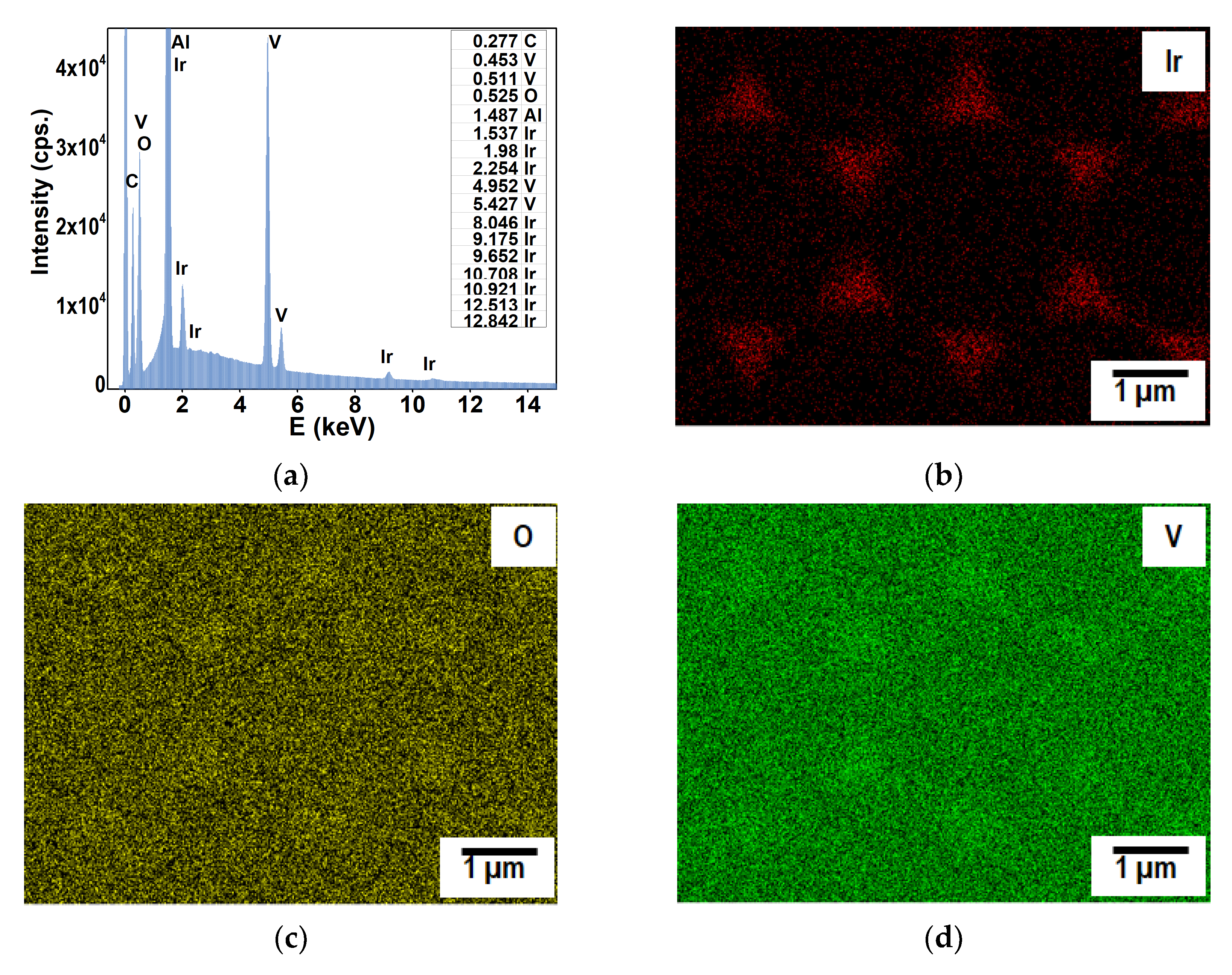
3.2.2. Compositional Characteristics of the VO2–Ir Microtriangles Composite

The chemical composition of the samples is assessed using Energy Dispersive X-ray Spectroscopy (EDS). In Figure 4a, EDS investigations show only the anticipated chemical elements’ (Ir, V, O and Al) presence in the samples. The Ir, V and O are associated with the composites and Al (plus O) comes from the substrate. The carbon peak is linked to a thin conductive coverage carbon layer for the EDS investigations.
Figure 4b–d shows the elemental maps (distribution) obtained by EDS for each chemical element of the composite. The particular element concentrations (Ir, V and O) are mapped across an area from Figure 3a. In Figure 4b, the presence of Ir microtriangles in the composite is seen as an increase red color intensity in the elemental map; Figure 4c,d reveals that V and O are evenly distributed on the surface of the composite. The uniform distribution of V and O proves that the Ir microtriangles are fully covered by a VO2 layer (confirmed by AFM in Figure 3a). Following the chemical composition analysis, the composite architecture is confirmed and the presence of VO2 validates the synthesis procedure and acts as a “blanket” on top of the Ir microtriangles.

3.3. Specific Optical Properties of the VO2–Ir Composite

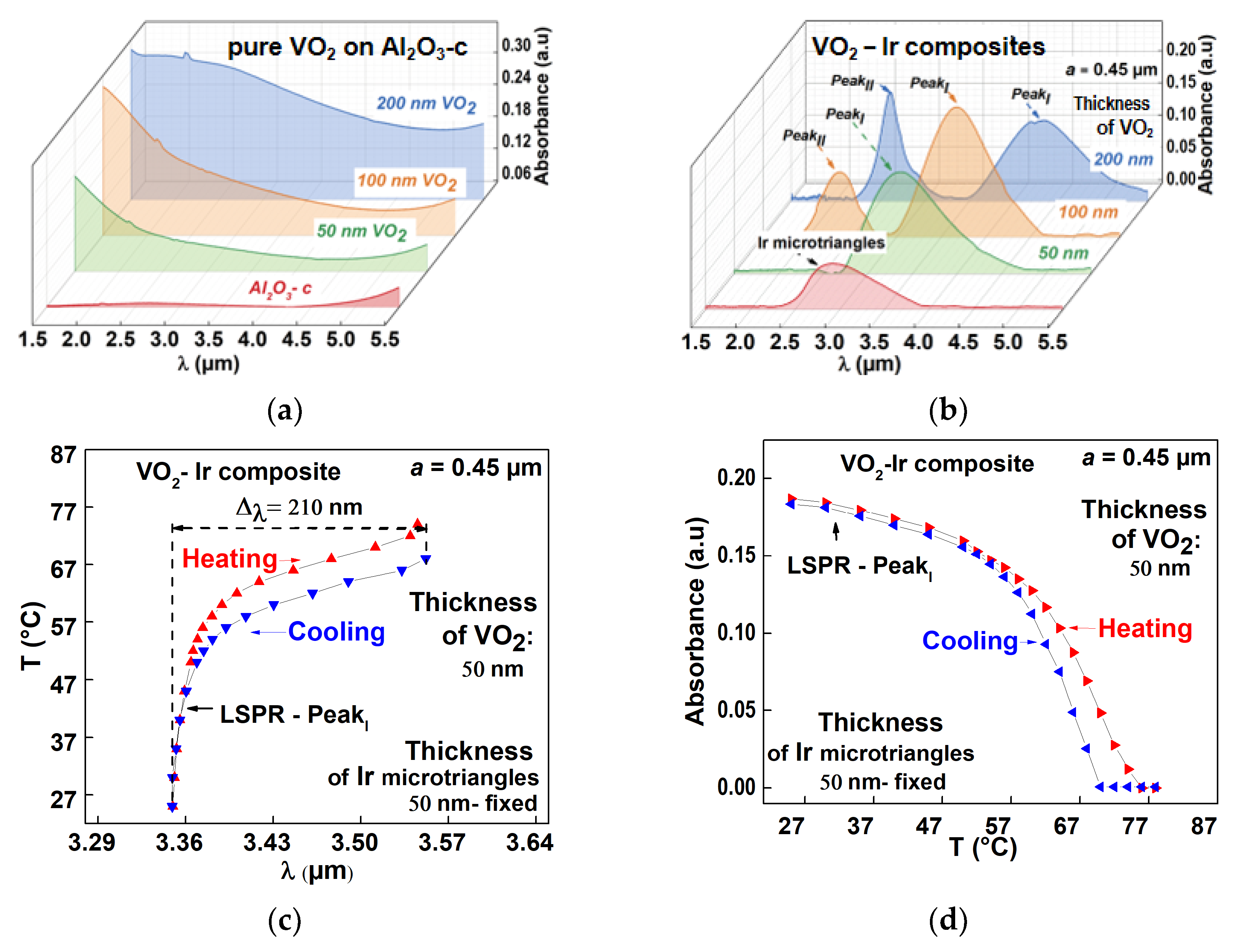
3.3.1. VO2–Ir Microtriangles Composite’s Optical Transmittance Characteristics

The optical properties in terms of the light transmittance of VO2 are dependent on the temperature. At room temperature, VO2 is transparent to near infrared light but as the measurement is performed at a temperature closer to the MIT temperature (i.e., around 68 °C) the light transmittance decreases and can reach a minimum depending on the thickness. Characteristics such as MIT temperature, transition hysteresis and transmission contrast depend on the intrinsic and extrinsic properties of the VO2 composite. The presence of Ir microtriangles can obviously affect the quality of the transition. Figure 5 makes a direct comparison between the optical characteristics of VO2–Ir composites and original VO2 samples. Except for the metallic sketch (presence of Ir microtriangles in the composites), all the other deposition parameters are the same. Figure 5a–c shows the temperature dependence of the light transmittance of the composites vs. VO2 samples. At room temperature, the transmittance is dependent on the thickness of VO2 and on the presence of Ir microtriangles. The light transmittance measured at 1.5 µm for the composites is approximatively 15% lower compared to the one of pristine VO2 samples (for a 200-nanometer thickness). This 15% transmittance difference fits well with the approximatively 9% coverage of Ir microtriangles on the substrate surface. When comparing the optical transmittance of the composites made with 0.45 µm vs. 0.70 µm Ir microtriangles (data are not presented here) no difference is pointed out, as is to be expected since the microtriangle-substrate coverage is equivalent. If the temperature increases, all the samples show similar optical transmittance characters to reach a thickness-dependent minimum above the MIT temperature. The hysteresis areas are approximatively constant, meaning that the matrices of VO2 are preserving their flexibility in temperature.
The difference between the extrema of the first derivatives (see Figure 5c,d) of the temperature-dependent optical transmittance shows that the average hysteresis width of the composites is close to 6 °C, equal to that of the VO2 thin films. The MIT temperature is approximatively 75 °C, when the thickness of the VO2 is 200 nm, which proves that the quality of the VO2 component of the composites is preserved. The slight shift of the MIT temperature (75 °C compared to the reference 68 °C) is a direct consequence of a weak strain inside the VO2 thin film, as discussed previously.

3.3.2. Plasmonic Properties of the VO2–Ir Microtriangles Composites

The dependence of the optical absorbance vs. wavelength for different VO2 thicknesses (50, 100 and 200 nm) is presented in Figure 6a. In the 1.5–5.5 µm range, the global absorbance value increases with the thickness. These curves are references useful to estimate the contribution of VO2 films on the absorbance spectra of the composites. These baselines are subtracted from the global absorbance spectra of the composite in order to extract the absorbance spectra of the zones with Ir microtriangles plotted in Figure 6b.
The composites exhibit several surface plasmon resonances that correspond to multiple absorbance peaks. The origin of these localized absorptions lies in the Ir microtriangles component and peak effects of the metallic architecture [29].
The absorbance spectra of the Ir microtriangles array, without matrix contribution, show an absorption peak in the infrared part of the electromagnetic spectrum (Figure 6b). This absorption peak is identified as the localized surface plasmon resonance properties of the Ir geometric architecture and is dependent on the dimension of each microtriangle. For Ir microtriangles with the typical dimension of a = 0.45 µm (resp. a = 0.7 µm), the LSPR maximum is localized at λLSPR = 2.95 µm (resp. λLSPR = 4.40 µm) and is strongly affected by the surroundings, as shown by the absorbance spectra of the composites measured as a function of thickness (Figure 6b). The absorbance spectra of the composites are measured as a function of thickness. The LSPR peaks of the composites shift to higher wavelengths with an increasing VO2 thickness (Figure 6b). This is due to the sensitivity and dependence of the triangles’ LSPRs to the dielectric environment [30].
Taking the benefit of the MIT transition of the VO2 matrix, the composites present modulable LSPR (in position and amplitude) (Figure 6c,d). As the temperature increases, the LSPR peaks of the composites will start to shift to a higher wavelength compared to their room temperature position. The LSPR peak shift is due to the temperature-dependent dielectric characteristics of VO2 that are transferred to the composites. For a 50-nanometer composite made, including 0.45 µm Ir microtriangles (Figure 6c), the LSPR position modulation (extracted using a Voigt function) is equal to 210 nm (3.34 µm to 3.55 µm). For the same composite, the LSPR amplitude temperature induced modulation varies between 0.18 to 0 (a.u.) (Figure 6d). Cooling the samples from 80° C to room temperature, induces “a return” of the LSPR peaks back to their original position and amplitude, also revealing the hysteresis of the composites. An active LSPR temperature modulation (position and amplitude) was obtained for all the composite’s configurations. The LSPR peak shifts and positions observed from different configurations of the composites are summarized in Table 1. The LSPR adaptability can be effective in the order of several hundreds of nanometers, up to 400 nm of magnitude, a very large scale with respect to the near infrared regime. The position of the LSPR peaks of the VO2–Ir composites is solely related to the influence of the VO2 matrix on the Ir microtriangles plasmonic properties. Ir microtriangles keep their own shape and size, which do not affect the LSPR compared to the system VO2–gold nanoparticles. By selecting the appropriate size of the Ir microtriangles and the thickness of the VO2 layer, the LSPR peaks can be tuned to the desired wavelength, making this VO2–Ir composite a promising candidate for the development of specific near infrared surface plasmon resonance-based applications.

4. Conclusions

Through the combination of Langmuir–Blodgett colloidal lithography and Pulsed Laser Deposition processes, the development of composites based on Vanadium dioxide and Iridium is achieved. The composites have similar characteristic in terms of structure and composition to that of their pure constituents. The similar optical transmittance of the composites and pure VO2 thin films proves that Vanadium dioxide preserves its integrity and intrinsic properties. The composites show LSPR properties in the infrared part of the electromagnetic spectrum. The position and amplitude of the LSPR peaks can be controlled and modulated through the size of the Iridium microtriangles and the thickness of the VO2. Furthermore, the LSPR position and amplitude of this smart composite can be actively tuned and modulated acting on temperature. A small change from 25 to 80 °C of the temperature composites can induce a maximum of 400-nanometer shift in the position of LSPR.

Author Contributions

Conceptualization, A.I.B., C.D.C. and F.D.-B.; formal analysis, A.I.B., C.D.C., C.C. and F.D.-B.; writing—original draft, A.I.B. and F.D.-B.; writing—review and editing, A.I.B., F.D.-B., C.C. and C.D.C. All authors have read and agreed to the published version of the manuscript.

Funding

This work benefited partially from government support managed by the French National Research Agency under the Investments for the future program with the reference ANR-10-LABX-0074-01 Sigma-LIM − LabEx ∑-lim (50% of Adrian BERCEA’s PhD thesis), laboratory of excellence launched by the French Ministry of Higher Education and Research between the XLIM Research Institute (https://www.xlim.fr) and IRCER (https://www.ircer.fr), pooling significant financial resources (https://www.unilim.fr/labex-sigma-lim).

Institutional Review Board Statement

Not applicable.

Informed Consent Statement

Not applicable.

Data Availability Statement

Not applicable.

Acknowledgments

This work benefited from technical support from CARMALIM platform regrouping instruments and investigation techniques of the University of Limoges, France.

Conflicts of Interest

The authors declare no conflict of interest.

References

  1. Ghidini, M.; Asti, G.; Pellicelli, R.; Pernechele, C.; Solzi, M. Hard–Soft composite magnets. J. Magn. Magn. Mater. 2007, 316, 159–165. [Google Scholar] [CrossRef]
  2. Wei, H.; Xu, H. Plasmonics in composite nanostructures. Mater. Today 2014, 17, 372–380. [Google Scholar] [CrossRef]
  3. Gaudin, M.; Carles, P.; Laborde, E.; Champeaux, C.; Dumas-Bouchiat, F. A dual nanosecond-pulsed laser setup for nanocomposite synthesis—Ag nanoparticles in Al2O3/VO2 matrix. J. Appl. Phys. 2019, 125, 054301. [Google Scholar] [CrossRef]
  4. Chen, Y.M.; Cai, J.H.; Huang, Y.S.; Lee, K.Y.; Tsai, D.S. Preparation and characterization of iridium dioxide–Carbon nanotube nanocomposites for supercapacitors. Nanotechnology 2011, 22, 115706. [Google Scholar] [CrossRef]
  5. Morin, F.J. Oxides Which Show a Metal-to-Insulator Transition at the Neel Temperature. Phys. Rev. Lett. 1959, 3, 34–36. [Google Scholar] [CrossRef]
  6. Dumas-Bouchiat, F.; Champeaux, C.; Catherinot, A.; Crunteanu, A.; Blondy, P. rf-microwave switches based on reversible semiconductor-metal transition of VO2 thin films synthesized by pulsed-laser deposition. Appl. Phys. Lett. 2007, 91, 223505. [Google Scholar] [CrossRef]
  7. Forero-Sandoval, I.Y.; Chan-Espinoza, J.A.; Ordonez-Miranda, J.; Alvarado-Gil, J.J.; Dumas-Bouchiat, F.; Champeaux, C.; Joulain, K.; Ezzahri, Y.; Drevillon, J.; Gomez-Heredia, C.L.; et al. VO2 Substrate Effect on the Thermal Rectification of a Far-Field Radiative Diode. Phys. Rev. Appl. 2020, 14, 034023. [Google Scholar] [CrossRef]
  8. Sadiq, M.N.; Roy, M.L.; Perennec, A.; Laurent, P.; Martin, N.; Passerieux, D.; Crunteanu, A.; Boyer, R.; Dumas-Bouchiat, F.; Martin, M.-B.; et al. Design and Characterisation of VO2 Based Switches for Ultra-Fast Reconfigurable Devices. In Proceedings of the 2019 IEEE MTT-S International Microwave Workshop Series on Advanced Materials and Processes for RF and THz Applications (IMWS-AMP), Bochum, Germany, 16–18 July 2019; pp. 172–174. [Google Scholar] [CrossRef]
  9. Stinson, H.T.; Sternbach, A.; Najera, O.; Jing, R.; Mcleod, A.S.; Slusar, T.V.; Mueller, A.; Anderegg, L.; Kim, H.T.; Rozenberg, M.; et al. Imaging the nanoscale phase separation in vanadium dioxide thin films at terahertz frequencies. Nat. Commun. 2018, 9, 3604. [Google Scholar] [CrossRef] [Green Version]
  10. Shao, Z.; Cao, X.; Luo, H.; Jin, P. Recent progress in the phase-transition mechanism and modulation of vanadium dioxide materials. NPG Asia Mater. 2018, 10, 581–605. [Google Scholar] [CrossRef] [Green Version]
  11. Kumi-Barimah, E.; Anagnostou, D.E.; Jose, G. Phase changeable vanadium dioxide (VO2) thin films grown from vanadium pentoxide (V2O5) using femtosecond pulsed laser deposition. AIP Adv. 2020, 10, 065225. [Google Scholar] [CrossRef]
  12. Liu, K.; Lee, S.; Yang, S.; Delaire, O.; Wu, J. Recent progresses on physics and applications of vanadium dioxide. Mater. Today 2018, 21, 875–896. [Google Scholar] [CrossRef] [Green Version]
  13. Guo, P.; Biegler, Z.; Back, T.; Sarangan, A. Vanadium dioxide phase change thin films produced by thermal oxidation of metallic vanadium. Thin Solid Films 2020, 707, 138117. [Google Scholar] [CrossRef]
  14. Nag, J.; Haglund, R.F., Jr. Synthesis of vanadium dioxide thin films and nanoparticles. J. Phys. Condens. Matter 2008, 20, 264016. [Google Scholar] [CrossRef]
  15. Garry, G.; Durand, O.; Lordereau, A. Structural, electrical and optical properties of pulsed laser deposited VO2 thin films on R- and C-sapphire planes. Thin Solid Films 2004, 453–454, 427–430. [Google Scholar] [CrossRef]
  16. Soltani, M.; Chaker, M.; Haddad, E.; Kruzelecky, R.V.; Nikanpour, D. Optical switching of vanadium dioxide thin films deposited by reactive pulsed laser deposition. J. Vac. Sci. Technol. A 2004, 22, 859–864. [Google Scholar] [CrossRef]
  17. Mattinen, M.; Hämäläinen, J.; Vehkamäki, M.; Heikkilä, M.J.; Mizohata, K.; Jalkanen, P.; Räisänen, J.; Ritala, M.; Leskelä, M. Atomic Layer Deposition of Iridium Thin Films Using Sequential Oxygen and Hydrogen Pulses. J. Phys. Chem. C 2016, 120, 15235–15243. [Google Scholar] [CrossRef]
  18. Galeazzi, M.; Chen, C.; Cohn, J.L.; Gundersen, J.O. Iridium thin films deposited via pulsed laser deposition for future applications as transition-edge sensors. Nucl. Instrum. Methods Phys. Res. 2004, 520, 293–295. [Google Scholar] [CrossRef]
  19. Ferrara, D.W.; Nag, J.; MacQuarrie, E.R.; Kaye, A.B.; Haglund, R.F. Plasmonic Probe of the Semiconductor to Metal Phase Transition in Vanadium Dioxide. Nano Lett. 2013, 13, 4169–4175. [Google Scholar] [CrossRef]
  20. Xu, G.; Chen, Y.; Tazawa, M.; Jin, P. Surface Plasmon Resonance of Silver Nanoparticles on Vanadium Dioxide. J. Phys. Chem. B 2006, 110, 2051–2056. [Google Scholar] [CrossRef]
  21. Takeya, H.; Frame, J.; Tanaka, T.; Urade, Y.; Fang, X.; Kubo, W. Bolometric photodetection using plasmon-assisted resistivity change in vanadium dioxide. Sci. Rep. 2018, 8, 12764. [Google Scholar] [CrossRef]
  22. Kallepalli, L.N.D.; Constantinescu, C.; Delaporte, P.; Utéza, O.; Grojo, D. Ultra-high ordered, centimeter scale preparation of microsphere Langmuir films. J. Colloid Interface Sci. 2015, 446, 237–243. [Google Scholar] [CrossRef]
  23. Lotito, V.; Zambelli, T. Approaches to self-assembly of colloidal monolayers: A guide for nanotechnologists. Adv. Colloid Interface Sci. 2017, 246, 217–274. [Google Scholar] [CrossRef]
  24. Van Dommelen, R.; Fanzio, P.; Sasso, L. Surface self-assembly of colloidal crystals for micro- and nano-patterning. Adv. Colloid Interface Sci. 2018, 251, 97–114. [Google Scholar] [CrossRef] [PubMed]
  25. Stavroulakis, P.; Boden, S.; Johnson, T.; Bagnall, D.M. Suppression of backscattered diffraction from sub-wavelength “moth-eye” arrays. Opt. Express 2013, 21, 1–11. [Google Scholar] [CrossRef] [PubMed] [Green Version]
  26. McGee, R.; Goswami, A.; Pal, S.; Schofield, K.; Bukhari, S.A.M.; Thundat, T. Sharpness and intensity modulation of the metal-insulator transition in ultrathin VO2 films by interfacial structure manipulation. Phys. Rev. Mater. 2018, 2, 034605. [Google Scholar] [CrossRef]
  27. Yang, M.; Yang, Y.; Hong, B.; Wang, L.; Luo, Z.; Li, X.; Kang, C.; Li, M.; Zong, H.; Gao, C. Surface-growth-mode-induced strain effects on the metal–insulator transition in epitaxial vanadium dioxide thin films. RSC Adv. 2015, 5, 80122–80128. [Google Scholar] [CrossRef]
  28. Fan, L.L.; Chen, S.; Luo, Z.L.; Liu, Q.H.; Wu, Y.F.; Song, L.; Ji, D.X.; Wang, P.; Chu, W.S.; Gao, C.; et al. Strain Dynamics of Ultrathin VO2 Film Grown on TiO2 (001) and the Associated Phase Transition Modulation. Nano Lett. 2014, 14, 4036–4043. [Google Scholar] [CrossRef]
  29. Liu, J.; He, H.; Xiao, D.; Yin, S.; Ji, W.; Jiang, S.; Luo, D.; Wang, B.; Liu, Y. Recent Advances of Plasmonic Nanoparticles and their Applications. Materials 2018, 11, 1833. [Google Scholar] [CrossRef] [Green Version]
  30. Jensen, T.R.; Malinsky, M.D.; Haynes, C.L.; Van Duyne, R.P. Nanosphere Lithography:  Tunable Localized Surface Plasmon Resonance Spectra of Silver Nanoparticles. J. Phys. Chem. B 2000, 104, 10549–10556. [Google Scholar] [CrossRef]
Figure 1. VO2–Ir microtriangles composites’ manufacturing pathway. (a) Photography of a perpendicular substrate covering by polystyrene spheres (P-spheres). (b) Schematic of spheres (P-spheres) compact arrangement. (c) Photography of a pulsed laser deposition process.
Jcs 05 00193 g001
Figure 2. Temperature dependence of the 2D arrangement of polystyrene microspheres (P-spheres) with a 3-micrometer diameter on an Al2O3-c substrate: (a) P-spheres deposited at 20 °C using Langmuir–Blodgett colloidal lithography (LB); (b) P-spheres deposited at 25 °C using LB; (c) P-spheres deposited at 30 °C using LB. The insert images in Figure 2 represent the Fast Fourier transform (FFT) of the underlaying optical images of the LB results.
Jcs 05 00193 g002
Figure 3. VO2–Ir microtriangles composite’s morphological and structural characteristics: (a) AFM image; (b) θ-2θ XRD patterns; (c) Zoom on a part of (b) XRD patterns from 39.6° to 41° θ-2θ XRD patterns of the composite. The thickness of the Iridium triangles within the composite is fixed to 50 nm, while the VO2 thickness is 50, 100 and 200 nm. The dotted lines in image (c) correspond to the theoretical position of VO2 and Iridium.
Jcs 05 00193 g003
Figure 4. Energy Dispersive X-ray Spectroscopy and Elemental mapping of a VO2–Ir composite. The thickness of VO2 200 nm and the “a” parameter of Ir microtriangles is equal to 0.70 µm (a) EDS elemental analyses of the composite; (b) Elemental map of Ir microtriangles; (c) Elemental map of Oxygen; (d) Elemental map of Vanadium.
Jcs 05 00193 g004
Figure 5. Optical characteristics of VO2–Ir microtriangles composites vs. VO2 thin films on Al2O3-c substrate: Temperature dependence of the light transmittance of (a) 50, 100 and 200 nm pure VO2 thin films; (b) composites made with 0.45 µm Ir microtriangles in 50, 100 and 200 nm VO2 matrix; (c) Temperature dependence of the first derivative of transmittance of VO2 thin films extracted from (a); (d) Temperature dependence of the first derivative of transmittance of composite made with 0.45 µm Ir microtriangles, extracted from (b).
Jcs 05 00193 g005aJcs 05 00193 g005b
Figure 6. Optical absorbance spectra (calculated as Absorbance = 2-log (Transmittance (%))) of composites vs. of VO2 thin films; (a) Optical absorbance spectra of VO2 thin films and Al2O3 substrate alone; (b) Optical absorbance spectra of composite and of the Ir microtriangles array; (c) Temperature evolution of the LSPR position of a 50-nanometer composite made with 0.45 µm Ir microtriangles; (d) Temperature evolution of the LSPR amplitude of a 50-nanometer composite made with 0.45 µm Ir triangles. The LSPR position/amplitude are extracted using a Voigt fit function of the temperature dependent absorbance spectra.
Jcs 05 00193 g006
Table 1. The position and active modulation values of the VO2–Ir microtriangles composite’s localized surface plasmon resonances.
Ir Microtriangles
a”—Characteristic Size
VO2–Ir Composite
Thickness of VO2 Matrix (nm)
LSPR PeakI
Position/Tunability
LSPR PeakII
Position/Tunability
0.45 µm503.34 µm/210 nm-
1003.68 µm/396 nm2.35 µm/150 nm
2004.26 µm/196 nm2.60 µm/100 nm
0.70 µm504.71 µm/123 nm-
100-3.43 µm/120 nm
200-3.91 µm/134 nm
Publisher’s Note: MDPI stays neutral with regard to jurisdictional claims in published maps and institutional affiliations.

