A Survey of ReRAM-Based Architectures for Processing-In-Memory and Neural Networks


Department of Computer Science and Engineering, IIT Hyderabad, Telangana 502285, India
Mach. Learn. Knowl. Extr. 2019, 1(1), 75-114; https://0-doi-org.brum.beds.ac.uk/10.3390/make1010005
Submission received: 15 March 2018
/
Revised: 16 April 2018
/
Accepted: 26 April 2018
/
Published: 30 April 2018
(This article belongs to the Section Network)
Abstract
:As data movement operations and power-budget become key bottlenecks in the design of computing systems, the interest in unconventional approaches such as processing-in-memory (PIM), machine learning (ML), and especially neural network (NN)-based accelerators has grown significantly. Resistive random access memory (ReRAM) is a promising technology for efficiently architecting PIM- and NN-based accelerators due to its capabilities to work as both: High-density/low-energy storage and in-memory computation/search engine. In this paper, we present a survey of techniques for designing ReRAM-based PIM and NN architectures. By classifying the techniques based on key parameters, we underscore their similarities and differences. This paper will be valuable for computer architects, chip designers and researchers in the area of machine learning.
1. Introduction
In recent years, the interest in machine learning and especially neural-network based techniques has grown significantly. Since conventional processing units such as CPUs and GPUs do not match the characteristics of machine learning (ML) algorithms, researchers have proposed novel hardware architectures for accelerating these algorithms [1]. On the processor front, the von-Neumann style compute-centric architectures are become increasingly constrained by data movement energy and memory bandwidth, since the data movement between the core and off-chip memory incurs 100× higher energy than a floating-point operation [2,3]. To address this issue, researchers have proposed “processing in/near memory” (also called near-data processing) whereby the computation logic is placed inside memory or the characteristic of memory itself is exploited for performing computations [4,5]. This approach avoids data movement completely and, thus, promises to break the memory wall.
For design of ML accelerators and processing-in-memory (PIM) solutions, emerging memories, such as resistive RAM (ReRAM) offer distinct advantages over conventional CMOS (complementary metal–oxide–semiconductor) based designs [6,7]. In the CMOS-based approach, modeling a neuron requires tens of transistors. In addition, SRAM (static random access memory) is a volatile memory with high leakage energy [8] and, since SRAM does not efficiently support a wide range of operations in memory, SRAM-based designs such as TrueNorth [1] use separate logic for performing computations. By comparison, ReRAM is a non-volatile memory with near-zero leakage energy and high density. The ReRAM state reflects the current passed through it in the history and this is very useful for modeling the synaptic weights of neurological synapses and implementing neural network (NN) architectures [9,10,11]. In addition, ReRAM supports operations such as analog matrix-vector multiplication (MVM), search and bitwise operations within memory which facilities energy-efficient accelerator design. For example, since the CONV (convolution) operation in convolutional neural networks (CNNs) involves MVM, and CONV layers account for more than 95% of computations in CNNs, ReRAM-based processing engine can boost the efficiency of CNNs significantly [12,13]. These factors have motivated researchers to implement a variety of ML/NN architectures on ReRAM, such as multi-layer perceptron [14,15], CNN [16,17,18], tensorized NN [19] and auto-associative memory [14].
Use of ReRAM for designing neuromorphic computing systems (NCSs), however, also presents challenges. For example, ReRAM has several reliability issues, such as limited write endurance, resistance drift, susceptibility to process variation (PV), etc. [20,21,22,23]. Analog operation exacerbates these challenges and also brings area/energy overheads of ADCs/DACs (analog-to-digital converters/digital-to-analog converters). Further, precise tuning of ReRAM requires frequent update of weights and large number of training iterations which incurs high overhead due to the high write energy and latency of ReRAM [24,25]. This presents challenges in achieving high throughput and accuracy. Addressing these challenges using (micro)architectural and system-level techniques is vital for ensuring adoption of ReRAM in state-of-the-art neuromorphic computing systems (NCSs). Several recent techniques seek to fulfill this need.
In this paper, we present a survey of ReRAM-based architectures for processing-in-memory and machine learning (especially neural networks) approaches. Figure 1 presents the overview of the paper. Section 2 provides the background and discusses the challenges in architecting ReRAM-based accelerators. It further provides a classification of the research works along several dimensions. Section 3 discusses ReRAM-based ANN (artificial neural network) architectures and management techniques and Section 4 reviews techniques for improving their reliability. ReRAM-based PIM techniques and spiking neural network (SNN) architectures are discussed in Section 5 and Section 6, respectively. Even though many of the works fall into multiple categories, we discuss them under single category only. Section 7 concludes this paper with a discussion of future challenges.
To achieve a balance between brevity and breadth, we limit the scope of this paper as follows. We include techniques implemented using ReRAM, although other emerging memories such as SOT-RAM (spin orbit torque RAM) and STT-RAM (spin transfer torque RAM) also provide PIM capabilities. Since different research projects use different evaluation platform and workloads, we focus on their qualitative insights and do not generally include quantitative results. We focus on (micro)architectural and system-level techniques and not device-level techniques. This paper is expected to be useful for researchers, system-architects and chip-designers.
2. Background and Overview
We now review some terms and concepts which are useful throughout this article. We refer the reader to previous work for a comprehensive background on non-volatile memories and their reliability issues [26,27,28], hardware architectures for machine learning [29], deep neural networks [30] spiking neural networks [1,31] and processing-in-memory [32].
2.1. Preliminaries
Machine learning architectures operate in two phases: training (learning) and testing (inference). In training phase, the relationship between the inputs and outputs of the system being modeled are learnt and, in the inference phase, the output is predicted for a given input. Neural network is an ML approach modeled after biological nerve system, which predicts the output by computing a non-linear function on the weighted sum of the inputs. There are two major flavors of NNs: ANNs and SNNs. ANNs are functional models of neurons, whereas SNNs mimic the brain operations more closely. A CNN has multiple convolutional (CONV), pooling and fully-connected (FC) layers in a multilayer NN design. A deep neural network (DNN) refers to an ANN with several hidden layers between the input and the output layers. In a binarized NN, both the feature maps and the weights are binary (+1 and −1) values.
Process variation refers to the deviation in parameters from their nominal values [33]. A hard fault refers to a situation where a cell is stuck at the value 0 or 1, which happens when the write endurance limit of a cell has been reached [34]. Resistance drift refers to change in the resistance of the cell over time and, hence, it can lead to a soft-error [28]. Sneak-paths are undesired paths for current-flow which exist in parallel to the desired path.
2.2. Using ReRAM as a Dot-Product Engine
Figure 2 shows the use of memristor for performing dot-product computation. Each bitline connects to each wordline through a ReRAM cell. Let R and G denote the resistance and conductance of a cell, where . If the cells in a column are programmed such that their conductance values are , , … . On applying the voltages , , … to these k rows, a current of current passes from the cell into bitline, as per Ohm’s law. Then, from Kirchoff’s law, the total current from the bitline is the sum of currents flowing through each column, as shown in Figure 2a. The total current (I) is the dot-product of input voltages at each row (V) and cell conductances (G) in a column, that is, . In terms of NN, the synaptic weights of neurons are encoded as conductances of the ReRAM cells. Then, the total current is the output of neuron in a CNN output filter. As shown in Figure 2b, the memristor crossbar array (MCA) achieves very high parallelism and can perform MVM in a single time step.
In addition to working as an MVM engine, ReRAM can also be used for implementing logical/bitwise operations, search operations, as we show later in this paper.
2.3. Challenges in Using ReRAM
The use of ReRAM also presents several challenges:
Challenges in Analog Domain: Operation in analog domain brings several challenges, e.g., noise, non-zero wire resistance, nonlinear I-V characteristics, I/O stage resistance, etc. In addition, storing intermediary analog outcomes and implementing max pooling in analog domain is challenging [35]. Further, on using analog circuitry, communication with the digital circuitry necessitates use of ADCs/DACs, however, these degrade signal precision and incur area/energy overheads. For example, ADC/DAC can take 85% [36] to 98% [18] of the total area/power of an neuromorphic computing system (NCS). Compared to this, digital signal transfer allows better control and high-frequency operation.
Reliability Challenges of ReRAM: The high defect rate and PV leads to reliability issues [21,37]. For example, due to “single-bit failure”, a cell may get stuck at high or low conductance value, called stuck-at-one or stuck-at-zero (SA1/SA0), respectively. Especially for large NCSs, a ReRAM implementation leads to heavy wire congestion and poor reliability of read/write operations due to voltage-drop and PV [38]. With increasing device failure rate, the accuracy of NN reduces drastically. To mitigate this issue, redundancy-based techniques can be used, however, they incur complexity and area overheads.
Challenges in Achieving High Accuracy and Performance: Compared to SRAM, ReRAM has high write energy/latency which increases the overall power consumption [39,40]. ReRAM limitations, e.g., series line resistance and sneak-path, further reduce the performance [41]. Further, during NN training, precise tuning of ReRAM requires frequent update of weights and large number of training iterations for convergence [24]. This leads to high number of writes and large energy consumption. The non-ideal characteristics of ReRAM, e.g., PV and abrupt behavior during SET operation further increase the overhead of ReRAM tuning [36]. Although the errors due to ReRAM faults or the analog-operation can be minimized by increased training, it leads to latency/energy penalty and aggravates ReRAM endurance issues [42]. In addition, retraining may not be sufficient in case of high fault rate [21].
2.4. Classification of Research Works
Table 1 presents a classification of research works on several parameters, e.g., NN architecture and ML phase. Table 1 also highlights several optimization strategies/goals and shows the works which compare ReRAM-based architectures with other approaches such as execution on FPGA (field programmable gate array) and GPU (graphics processing unit).
3. ReRAM-Based ANN Architectures
In this section, we discuss techniques for mapping a NN to ReRAM crossbar (Section 3.1), architectures for enabling NN inference (Section 3.2), architectures for enabling NN training (Section 3.3), MCA (memristor crossbar array) aware pruning strategies (Section 3.4) and reconfigurable designs (Section 3.5). We then review techniques for reducing overhead of analog operation (Section 3.6) and designing hybrid analog–digital or purely-digital systems (Section 3.7).
3.1. Mapping NN to ReRAM
Table 2 summarizes salient features of mapping schemes. We now review several of these schemes.
Hu et al. [73] developed an algorithm for transforming arbitrary matrix values into memristor conductances for minimizing inaccuracies in MVM while accounting for memristor crossbar array (MCA) circuit limitations. Figure 3 shows the overall flow of their technique. They used a MATLAB solver for crossbar simulation which is orders of magnitude faster than SPICE (simulation program with integrated circuit emphasis) simulator. They first linearly mapped a matrix to an ideal MCA which has zero wire resistance, zero I/O stage resistance, zero noise and perfectly linear I-V variation. Then, the algorithm simulates actual current and voltages on the realistic MCA by tuning the conductance values to match the current in every cross-point device in an ideal MCA (refer to “transformation” step in Figure 3). Pre-computed Jacobian matrix is used to accelerate the simulation and, thus, their method achieves high overall speed, e.g., an arbitrary matrix can be converted to a crossbar in few seconds. After this, close-loop tuning is used for programming memristors to the target conductance values (refer to “programming” step in Figure 3). Their technique allows arbitrarily changing the device resistance value and provides high resolution. Finally, input signals are applied to the MCA, and the MCA output is mapped to output signal (refer to “processing” step in Figure 3). The limitation of their approach is that they compute the mapping on an external processor and not on-chip. Their technique provides orders of magnitude higher performance-energy efficiency product than an ASIC implementation and also achieves high accuracy for an NN application.
Li et al. [62] presented a ReRAM-based inexact functional unit (iFU) which implements a three-layer NN that: (1) performs MVM of weights and inputs; and (2) computes sigmoid activation function. Of these, they mapped MVM to MCA and implement the sigmoid function using a sigmoidal neuron design [62]. By using multiple iFUs, high performance is achieved. DACs and ADCs are used for converting signals between digital and analog domain. For every task, iFUs are trained by adjusting the synaptic weights. Then, these weights are mapped to conductance states of ReRAM devices in the MCA using program-and-verify operations. Figure 4 shows the overall flow of their technique. Several complex functions that require thousands of cycles in a CPU can be performed in few cycles using their iFU. Their technique improves energy efficiency compared to CPU, FPGA and GPU.
Taha et al. [57] evaluated the design of an analog and a digital memristor-based neural core and compared them with an SRAM-based digital core, GPU and CPU. Figure 5 shows their proposed neural core architecture. With increasing size of crossbar, read energy also rises due to extra sneak paths. To address this, they used a tiled MCA design where only one row of tiles is accessed at a time. This restricts the leakage current present in an operation to that of a 4 × 4 crossbar. Thus, the dynamic energy consumption is reduced in comparison to that of an untiled MCA. Both digital and analog cores use tiled designs. In the digital core, SRAM arrays are substituted by the tiled MCAs. As for the analog core design, the tiled design allows all the tiles to be read concurrently with much lower latency than that in the digital core. It also allows elimination of multiple components used in digital core, e.g., memory array decoder, MAC (multiply-accumulate), etc. Use of diodes prevents alternate current paths. As for the write operation in the analog core, only a single row is written at a time during training, similar to the case of digital core. To reduce the complexity of ADCs/DACs, the precision of signals is assumed to be limited (4-bit). Results show that the designs can be ordered by increasing area and energy as: analog memristor core, digital memristor core, SRAM core, GPU and CPU. Specifically, their NN-based designs achieve magnitude-order higher energy and area efficiency compared to CPU and GPU.
Huang et al. [19] presented a 3D CMOS-ReRAM based accelerator for TNNs (tensor neural networks). As shown in Figure 6, their design has three layers: two-layers of ReRAM crossbar and one-layer of CMOS circuitry. The first ReRAM-crossbar layer works as a buffer for storing the weights and is used for configuring the crossbar resistance values in the second layer. The tensor cores are 3D matrices and its 2D slices are stored on Layer 1. The second layer of MCA executes operations such as vector addition and MVM. This layer receives tensor cores from the first layer over through-silicon-via (TSV) for performing parallel MVM. The third layer orchestrates the working of overall TNN. It generates tensor-core indices for initiating tensor-train matrix multiplication. This layer also performs the non-linear mapping.
For mapping a TNN on their design, first the NN compression is done using layer-wise training process. Then, the optimal NN design (e.g., layer-count and activation function) is found by exploring parameters such as bit-width, compression ratio, accuracy, etc. After this, architectural optimization of Layers 1 and 2 is performed to reduce read latency and energy. The TNN is mapped to their design in a folded manner by leveraging the sequential operation of every layer on the NN. The crossbars in Layer 2 perform parallel multiplication and their output is sent to the scalar core for accumulation. The output of scalar core is sent to the sigmoid function for activation in a pipelined manner. The activation matrix is used for the processing of next layer. Thus, the entire TNN inference can be mapped to their proposed design. Their technique achieves high amount of compression by using sparse representation of dense data in high-dimensional space. Their design achieves better performance and energy efficiency compared to ASIC (application-specific integrated circuit), CPU and GPU implementations.
Ni et al. [61] presented a technique for mapping binarized CNN on a sneak-path-free digital MCA. In binarized CNN, both the feature maps and weights are stored as binary values (+1 and −1). Hence, CONV can be achieved simply by binary dot-product instead of MVM. Every binary-CONV layer performs CONV on binary feature maps from previous layer and binary weights. The output of binary-CONV is processed by normalization layer and max-pooling layer. The output is fed to the binarization layer which provides binary non-linear activations based on the input sign.
They map all binary CNN operations such as CONV, batch normalization, pooling and activation on the digital MCA using unsigned bitwise operations. The works, which use two crossbars [12,74] to store negative and positive weights, require a subtract operation for every complementary bitline output. To avoid the need of subtract operation, they proposed converting signed binary CONV to unsigned binary XNOR, as shown in Table 3. It is clear that, by transforming +1/−1 values into 1/0 values (respectively), a multiplication operation can be transformed into XNOR operation. Since , they map A and as wordline inputs and W and as ReRAM conductances. This strategy requires only one inverter for every input.
Further, since the order of binarization and pooling has no impact on the overall output, the batch normalization and binarization can be combined. In addition, based on batch-normalization computations, a threshold is chosen to compare with the binary CONV output. For pooling, a single-output crossbar can be used and the comparator threshold can be suitably set to see whether any binarization result in the pooling region is 1. Compared to a non-binary CMOS implementation, their design achieves higher energy efficiency and performance with only minor loss in accuracy.
3.2. Architectures for NN Inference
Shafiee et al. [16] presented a CNN accelerator which uses MCAs for dot-product computations. Figure 7 shows their overall architecture. Since CONV and classifier layers perform dot-product, their technique is implemented for those layers. LRN (local response normalization) layers cannot be implemented using crossbars. The system has multiple tiles each designed with MCA which store synaptic weights and perform in-situ analog dot-product computations on them. Since a crossbar cannot be efficiently reprogrammed at runtime, one crossbar is assigned for processing a group of neurons in any CNN layer. Different CNN layers are pipelined which reduces the buffering requirement, increases throughput and allows using higher amount of chip resources for dot-product computations.
Since ADC/DAC contribute a large fraction of total overhead, they proposed strategies to reduce them. Each ADC is shared by multiple MCAs. Weights are stored as 16 b fixed-point values which suffices for many ML applications. A 16 b number is represented using 16 consecutive voltage levels, each recording 0/1 bit of the 16 b number. Product is computed as 16 sequential operations which requires only 1-bit DAC. A 16-bit synaptic weight is stored in w-bits cells of a single row (e.g., w = 2). Their partial products are merged using shifts and adds. When the weights in a column are collectively large, they are stored in inverted form which ensures that the MSB (most significant bit) of sum of products is always 1. This reduces the size of ADC by one bit. Due to (nearly) exponential relationship between the resolution and cost of ADC and the large contribution of ADC in overall power consumption, this optimization has large impact on overall efficiency. For representing negative weight values, crossbar inputs are provided as 2’s complement and the most significant bit is used as the sign bit. Their accelerator provides large improvement in throughput and energy compared to other near-data accelerators.
The limitation of their pipelined design is that it improves throughput and energy efficiency only when many inputs (e.g., images) can be successively fed to the accelerator. However, since images are analyzed in batches where images in the next batch are analyzed using updated weights, their deep pipeline suffers from bubbles and stalls [46]. Further, the digital circuitry such as shared data bus and eDRAM (embedded DRAM) buffer consumes large area, especially due to the wide ports in the eDRAM buffer.
Tang et al. [17] presented an area and energy-efficient memristor-based tiled architecture for accelerating DNNs, which is illustrated in Figure 8. Every tile has an MCA-based PE (processing engine) array, an eDRAM buffer, a register buffer and multiple DACs. The input feature maps of CNN are stored in the eDRAM buffer and is cached in the register buffer. The register buffer provides data for the CONV in current step and buffers the input data for the subsequent-step. The analog output signals from DACs are transmitted across horizontal PEs. The output of PE array and the partial sums of outputs are also saved in the eDRAM buffer and they are communicated across vertical PEs in digital domain. Every PE has an ADC, a logic block (including a shift unit and an accumulate unit) and two S&H (sample and hold) units. The ADC converts analog signals from the crossbar to digital signals for subsequent MAC operations. The accumulate unit performs accumulation operation: (1) between results of neighboring columns of crossbar; and (2) in CONV between neighboring PEs in the same column of the PE array. One S&H unit holds temporal analog data and another unit holds reused data between horizontal PEs. By using DACs in only one column of the PE array and not in all the PE arrays, their design reduces the number of DACs.
To map a CNN layer to a tile, multiple 3D CONV kernels of a layer are organized into an unfolded weight matrix. Since the low (e.g., 4-bit) resolution of a ReRAM cell is insufficient for storing a high-precision (e.g., 16 bits) weight, a 16-bit weight is stored in four neighboring elements in a single row and the 3D CONV kernel is stored in four neighboring columns. Their dataflow leverages three types of data reuse which allows reducing the port-width of eDRAM buffer. First, the crossbar performs MAC operations and the partial sums of CONV outputs are reused between vertical PEs. Second, analog signals are reused between horizontal PEs. Third, the register buffer allows input reuse.
They further noted that, in ReRAM-based NCSs, the resolution of ADC and DAC are related as . Here, “Rows” shows the number of ReRAM rows and shows the resolution of a ReRAM cell. Thus, the resolution of ADC needs to be high which exacerbates ADC power consumption. They propose reducing ADC resolution by leveraging the error-tolerance of DNNs and narrow values of weights/inputs/outputs in widely-used DNNs. Based on this, the input and weight values can be truncated and, thus, a tradeoff can be achieved between the overall precision and energy efficiency. Compared to other ReRAM-based NCS [16], their design reduces area and power consumption with negligible loss in accuracy.
3.3. Architectures for NN Training
Since NN training involves weight update and intricate data dependencies, most works only support interference, and assume that weights are updated only in the beginning. By comparison, some works present techniques for implementing NN training also in ReRAM. We now discuss some of these works.
Song et al. [46] presented a ReRAM-based pipelined design for accelerating both training and testing of CNNs. They divide MCAs into two types: memory and morphable. The morphable MCAs can perform both computation and data-storage and memory MCAs can only store data, such as results from morphable MCAs. Both forward and backward computations have data dependencies. The result of forward computations are stored in memory MCAs which are used in backward computations for generating errors and partial derivatives. Figure 9 shows their design for training a three-layer CNN. In the logical cycle T, input d enters morphable MCA (A1) which executes MVM. The results are written to the memory MCA (d). Continuing in this manner, the results of forward computation are saved in d. Backward computation starts in T, where errors (l shows the layer) and partial derivatives (W) are generated. First, the error for the third layer () is calculated in T and stored in a memory MCA. In T, two calculations happen concurrently which depend on : (1) partial derivative (∇W) is calculated by previous results in d and ; and (2) error () of the second layer is calculated from . Based on ∇W, weights in A3 and A32 are updated. Continuing in this way, ∇W is calculated in T.
Their design exploits both intra- and inter-layer parallelism. To exploit intra-layer parallelism, they note that, since the input to MCA in each cycle is large, mapping all the kernels to a single MCA leads to inefficient design. Hence, they map them to multiple MCAs and, then, collect and add their outputs. The number of duplicate copies of MCAs storing the same weight shows the granularity of parallelism and by choosing a right value of this, a trade-off between hardware overhead and throughput can be achieved. They further noted that, during training, the inputs processed before a weight-update (called a “batch”) do not have any dependency. Since batch size is much larger than one (e.g., 64), they propose a pipelined training architecture where inputs inside a batch can be processed in pipelined manner but the input of next batch can enter the pipeline only when the previous batch has been fully processed. To avoid the need of DACs, instead of voltage-level based input, they utilize a weighted spike-coding approach and its higher latency is tolerated by the pipelined design of different layers. To avoid the need of ADCs, they use “integration and fire” scheme which integrates analog currents and stores the generated output spikes in a counter. Compared to GPU implementation, their design achieves large improvement in performance and energy efficiency.
Cheng et al. [24] presented an architecture along with peripheral circuitry for enabling NN training in ReRAM. Their design provides support for back-propagation and weight-update and leverages peripheral circuitry for inference operation. The sense amplifier implements analog-to-digital conversion, ReLU and max functions and precision control. In deep reinforcement learning, max function may be performed on more than four (e.g., 18) values and, hence, they add more registers and multiplexors to implement this. Their design includes circuits for preprocessing and final-output difference. They further noted that for addressing the write-variability problem, some works iteratively RESET, read and initialize ReRAM which incurs large energy overhead. They presented a variability-free tuning strategy which reduces the frequency of reads/writes to ReRAM by avoiding unnecessary initialization, read and RESET operations. Furthermore, in ReRAM, SET/RESET operations happen abruptly/gradually, respectively, and, hence, they proposed a gradual-write strategy for avoiding error-prone SET operations. A synaptic weight is represented by two conductance values in ReRAM termed as positive/negative ReRAM, respectively. They performed only RESET operation in positive/negative ReRAM for reducing/increasing the weight, respectively. They show that for supervised learning and deep reinforcement learning, their design provides higher energy efficiency than an ASIC and a GPU implementation, respectively.
3.4. MCA-Aware Pruning Strategy
Ankit et al. [67] noted that pruning techniques lead to a network with irregular connections, as shown in Figure 10b,c. The resulting network may not match to the crossbar design and, hence, it may lead to inefficient hardware implementation. They proposed a technique for transforming DNNs for allowing efficient implementation on MCAs. Their technique prunes at the granularity of the MCA and not synapse, which helps in retaining the gains of algorithmic pruning and network sparsity in memristive NCSs. Their technique is applicable to FC layers, which show no data reuse and have most of the synapses of the network.
They propose a “Size-Constrained Iterative Clustering” (SCIC) algorithm transforms the connectivity structure of the DNN into multiple high-utilization clusters. SCIC is based on “spectral clustering”, a graph clustering algorithm which produces a group of disjoint graph nodes with the goal of maximizing intra-cluster associativity and minimizing inter-cluster associativity. These goals seek to produce clusters which can be mapped to MCAs with high utilization while also achieving high throughput. The SCIC algorithm seeks to minimize the number of unclustered synapses. It iteratively executes spectral clustering on the current connectivity matrix, until there is no more reduction in unclustered synapses. In every iteration, clusters mapping to MCAs with high utilization are selected and remaining clusters are merged with the present connectivity matrix. In each training iteration of backpropagation algorithm, first pruning is performed and, then, SCIC is applied. Upcoming training iterations recover the accuracy loss due to pruning. Thus, by removing ineffectual connections and unclustered synapses, their technique achieves a network which is maximally clustered and optimally pruned. Figure 10a summarizes the flow-diagram of their technique.
Figure 10b–d shows the connectivity matrix of a DNN before pruning, after conventional pruning and after employing their technique. Evidently, the irregular sparsity resulting from conventional pruning prohibits direct mapping to MCAs, whereas their technique creates smaller clusters which can be mapped to MCAs. They evaluated their technique on MLP (multi-layer perceptron) based SNNs and observe large savings in area and energy. Their technique allows mapping a DNN to MCAs of different sizes. They also showed that performing clustering after the training process cannot maintain the gains of sparsity in hardware implementation.
3.5. Reconfigurable Architectures
Zidan et al. [41] proposed a “field programmable crossbar array” (FPCA) which combines memory, analog and digital computing in a single core. This core can be dynamically reconfigured for handling various applications. For example, as shown in Figure 11, for three different applications (A, B and C), the cores/tiles that work as analog/digital-computing unit or memory unit can be altered. The parallelism of MCA is leveraged for performing compute and storage operations. Further, the resources are allocated in a manner to best match the computing requirements of the application. Their design consists of multiple “memory cores” (M-cores). Every M-core is a single crossbar which can perform computations using/inside local memory. Every M-core has multiple identical tiles that can be reconfigured to work as storage or digital/analog computing element. Thus, either an entire core or a tile can be assigned to a task, which allows multi-granularity reconfiguration to adapt to application needs. In addition, processing for an application can happen in a domain (digital or analog) which is optimal for it.
They noted that nearly all arithmetic operations such as matrix/trigonometric computations, multiply/divide/add, etc. are based on a tree-reduction circuit. They further noted that an arithmetic compressor works by counting the number of ONEs which can be easily achieved using the crossbar design. Figure 12a shows a single column of a crossbar where all rows are biased with a reading voltage (). The output current is shown as . Since and , we have , where shows the number of ones in the column. Further, by biasing only selected rows, masked tree-reduction can also be realized, as shown in Figure 12b. This reduces the overhead of implementing division/multiplication operations. This reduction can also be extended to multiple columns, as shown in Figure 12c.
Several tree reduction operations, including masked tree-reduction, can be concurrently performed on the same MCA. Thus, M-cores allow parallel in-memory processing. Using the arithmetic compressor, multiple arithmetic operations are performed concurrently in the M-core. For example, for vector addition, the number of ONEs in a column are written back to the M-core for the next iteration. This iterative procedure stops when then vector addition reduces to addition of two operands. Along similar lines, scalar/vector-vector/matrix-matrix multiplication can also be implemented. Thus, any arithmetic operation, except incrementing or two-operand addition, can be implemented using this approach.
They further proposed mapping NN architectures on binary ReRAM devices. In their design, the weights are encoded in N-bit binary format and then stored in N-devices instead of just one analog device, as shown in the Figure 13. Here, N-columns are equivalent to one analog column. Use of quantized weights allows reducing the value of N. The output of each column shows the sum of product of input current and binary weights of the column. After digitizing this and performing binary-scaling, the output of N columns are added to obtain equivalent analog dot-product. Compared to analog devices, use of binary devices allows storing the weights with higher accuracy and also achieving high performance and energy efficiency. They further discussed strategies to integrate FPCA at system-level. Their proposed design provides higher performance at lower power budgets compared to CPU, GPU and TrueNorth.
Zha et al. [56,70] presented a design which allows better programmability across memory–compute boundary for achieving in-memory computing. Their design has 2D array of tiles each containing an MCA and some connection nodes. The connection node has multiplexors, buffers, RAM cells for configuration, a flip-flop and a sense amplifier. Their design can reconfigure mat(s) in four possible modes, as shown in Figure 14. First, a mat can be configured to implement “TCAM function” (ternary content addressable memory) which is beneficial for search-based workloads. Second, in compute (logic) mode, their design allows arbitrary combinational logic or sequential logic (by using flip-flops), whereas other works use MCA for MVM only. Boolean inputs of a logic gate are applied to connection nodes and are converted into digital outputs. These outputs are sent to neighboring tiles as inputs and thus, direct data-flow computation can be performed based on the configuration.
Third, in interconnect mode, a mat can be utilized for both global and local routing which provides same function as switch/connection blocks in FPGA. Fourth, in memory mode, one mat works as a memory array and column address decoder. Three neighboring mats are configured as read/write column select logic and row address decoder, respectively. Based on the write enable signal, the direction of connection nodes is changed to achieve read/write operations.
Compared to a CMOS peripheral circuitry, their design reduces the overhead of connecting bulky CMOS circuitry with dense MCA. In addition, reconfigurability of row and column address decoders allows flexible adjustment of aspect ratio of memory block to gain desired performance and capacity. Their design allows partitioning the resources between compute, storage and interconnection for achieving best performance for each application. In FPGA, the size and location of memory blocks cannot be altered after they are manufactured, whereas their design allows this for efficiently exploiting data locality. Compared to FPGA, their design provides better performance at lower area; and these benefits are not merely because of substituting SRAM with ReRAM. In addition, compared to CPU, their design provides large speedup and energy savings.
3.6. Reducing Overhead of Analog Implementation
Table 4 summarizes the strategies for reducing overhead of analog domain operation. We now discuss several of these works.
Li et al. [58] presented a technique to avoid the need of using ADCs/DACs based on the idea that the memristor-based NCS can directly learn the relationship between the binary arrays representing digital I/O data. For instance, in an NCS with 2, 8 and 2 nodes in input/hidden/output layers (respectively), instead of converting digital signals to analog to provide input to NCS, their technique directly feeds digital signals to 16 input ports and, based on them, computes 16 digital outputs. Thus, their technique allows direct interfacing between memristor-based NCS and the digital system, as shown in Figure 15. Unlike in original NCS with ADCs/DACs, in their design, each port is independent and can be separately optimized. Specifically, by reducing the error rate of ports representing MSBs of a binary number, overall accuracy can be improved. For this, they modify the loss function of the training algorithm and assign larger/smaller weights to MSBs/LSBs (least significant bit), respectively. Due to this, an error in MSB leads to much higher penalty than the error in LSB and, hence, training process places higher effort on reducing MSB error for improving final accuracy. Although their technique increases the number of I/O ports and crossbar size greatly, overall area is still reduced due to avoidance of ADCs/DACs and high density of crossbar. In addition, since the outputs of their design are continuous analog signals, they use analog comparators (acting as 1-bit ADCs) for converting them into discrete binary digital signals. Compared with conventional architecture that uses ADCs/DACs, their technique reduces area and energy consumption while maintaining same accuracy on average.
Xia et al. [18] presented a technique to reduce the overhead of DACs/ADCs in ReRAM NCSs. They noted that, in different CONV layers of a CNN, on normalizing the output values by the maximum value in that layer, most of these values become zero; most of the remaining values are small; and only a small fraction of values are large. Hence, they first normalized the data, and then quantized intermediary data to 1-bit value. This can be directly used as the analog input for ReRAM crossbar and, hence, avoids the need of DACs. Since commonly-used functions such as ReLU and sigmoid increase monotonically, the neuron function can be merged into sense amplifier by using a corresponding reference. The threshold for quantization is searched for each layer separately using a greedy algorithm. In addition, since quantization after max pooling is equivalent to quantization before pooling using same threshold, they propose performing quantization before pooling, which reduces max pooling to an OR function of 1-bit inputs.
However, ADCs may still be required for merging ReRAM output signals with other results, for example, when the precision provided by a single crossbar is insufficient and, hence, multiple crossbars are required. To avoid the need of ADC in such cases, they used two ReRAM cells in a column to store the highest and the lowest bits of a given weight and use different bias voltages in the input ports to select one from them and achieve “shift and add” function. They also proposed solutions for the cases when merging is required because of the need of storing positive and negative weights in two crossbars and when weight matrix needs to be stored in multiple crossbars due to the CNN size exceeding that of ReRAM crossbar. Their technique brings large reduction in area and energy with negligible impact on classification accuracy.
Li et al. [35] notes that, in conventional training methods for MCA based NNs, first the parameters of memristors need to be found and then the MCA needs to be tuned to the target state. However, this process incurs latency/area/energy overhead and may also introduce errors. They proposed a mixed-signal framework for accelerating NN training. In “stochastic gradient descent algorithm” used for NN training, many multiplications are performed which are difficult to be realized in analog domain. To address this issue, they proposed approximating the error computations by ignoring values with small magnitude, such that the impact on the overall result is minimal. Further, they divide the weight update calculations into sign computation and numerical computation. Sign computation finds the direction of weight update and it can be realized through a zero-crossing detector and an analog comparator, as shown in Figure 16. The calculations between signs are realized in digital domain, which is beneficial also because the digital data can be cached more easily than the analog data. To avoid analog numerical computations, their technique automatically adjusts convergence rate and, if the convergence rate falls below a threshold, the training process is stopped. Further, convergence rate is multiplied with a random value between 0 and 1 to emulate fluctuation of values. To avoid caching the delta values and then importing them in the network, they use a copy crossbar which allows directly computing these values. Compared to a CPU implementation, their design achieves magnitude order higher performance and energy efficiency with only minor reduction in accuracy.
3.7. Analog–Digital Hybrid and Digital-Only Designs
Table 5 summarizes the domain of operation of different designs. We now discuss some of these works.
Liu et al. [14] designed an NN accelerator using on-chip MCAs, which is shown in Figure 17a. They used a hybrid signal representation where analog domain is used for computations in the MCAs and signal transfers between MCAs, whereas control signals remain in digital format for simplifying synchronization and communication between CPU and their accelerator. MCAs execute analog neuromorphic calculations. MCAs are organized in a centralized mesh topology to lower the cost of interconnection. MCAs are arranged in a hierarchical group structure and communication happens at both intra- and inter-group level. MCAs are connected using a mixed-signal interconnection network which helps in data migration and task mapping on MCAs. The analog datapath has input buffers and data multiplexors for connecting any input port to any output port, as shown in Figure 17b. They presented topology and routing strategies for both MLP and auto-associative memory (AAM) implementations of NN. Their accelerator boosts the performance and energy efficiency compared to the baseline CPU, a digital-only neural-processing unit design and a design where MCAs are connected using a digital-interconnection network.
Ni et al. [36] noted that, on using analog values, the error rate of intermediate states is much higher than that of terminal (ON/OFF) states, as shown in Figure 18. To remove unreliable intermediate values, they proposed a completely digital ReRAM crossbar design where only binary values are used and thus, ADC/DAC are not required. By comparing the column output voltage with the reference threshold at sense amplifier, the analog value is digitized. To reduce the information loss due to digitization, they increased the quantization level by using multiple thresholds. The thresholds are carefully selected so that most information can be preserved after digitization.
Further, they decomposed multiplication operation into three sub-operations which can be implemented on a binary crossbar (where N shows the number of bits). First, they divided MVM into multiple vector inner-product operations each of which are executed in parallel on one crossbar. If s denotes the output of inner-product, then the output of column j in ReRAM crossbar is given by if and 0 if . For example, if , then the output is equal to 11100000 (assuming ).
Second, the inner-product of first step is ascertained by the position where the bit value changes from 0 to 1. As such, to obtain the result index, XOR operation is performed on every neighboring pair of bits. For instance, if , then, after XOR operation, 11100000 changes to 001000000. Third, output of second step is taken and inner-product result (s) is produced in the binary format. For example, if , the binary value 00000011 is produced and, hence, a value of 1 is stored in Row 3. Thus, their MVM has binary input and binary output which obviates the need of ADCs/DACs. They show that compared to a CMOS-based ASIC, their implementation achieves lower area, energy and latency.
4. Improving Reliability of ReRAM-Based ANN Architectures
Table 6 shows the techniques that address various vulnerabilities and their key ideas. We now review the techniques for mitigating hard faults (Section 4.1) and resistance drift (Section 4.2).
4.1. Addressing Hard Faults
Chen et al. [47] proposed a fault-aware training scheme for ReRAM based NNs. Their technique first finds an optimal mapping of weights to memristors based on the weighted bipartite-matching algorithm. Since variation profile differs across memristors and large weights may get clustered due to sparse weight matrix of NN, in this mapping, large weight may get mapped to a ReRAM with high variation. To address this challenge, they noted that, due to the self-healing capability of NNs, loss in accuracy due to removal of some weights is automatically compensated during training by changing the neighboring weights. Hence, they trained NN based on the distribution of stuck-at-faults and resistance variation in crossbar and lowered the magnitude of weight mapped to a memristor with large variation/fault-rate, as shown in Figure 19. Their technique removes nearly all the loss in NN accuracy due to faults/variations in ReRAM.
Xia et al. [20] noted that hard faults in ReRAM due to manufacturing and limited endurance lead to poor accuracy in training of a ReRAM-based NN. Their technique detects faulty cells after a fixed number of iterations and tolerates the faults in subsequent training iteration by leveraging fault tolerance feature of NN. Figure 20 shows their fault-detection scheme. Here, first stuck-at-0 faults and then, stuck-at-1 faults are detected by seeing whether the value in the ReRAM can be updated properly. Since stuck-at-0/1 faults can happen only in cells with high/low resistance (respectively), only these cells are chosen for fault-detection, which reduces the latency of fault-detection operation.
Figure 21 illustrates their procedure for training. They note that small weights make little contribution to the accuracy, but reduce ReRAM lifetime significantly. Hence, in back-propagation phase, their technique flushes weights smaller than a threshold to zero, which is termed as “threshold-training” in Figure 21. This strategy boosts ReRAM lifetime while bringing only small increase in the number of training iterations. Further, since pruning schemes lead to a large fraction of weights becoming zero, they used this sparse-nature of NNs to tolerate stuck-at-0 faults. For this, rows/columns of the weight matrix are reordered to map zero weights to cells having stuck-at-0 faults. This is shown as “remapping” in Figure 21 and it requires on-line fault detection. For performing remapping, they employed genetic algorithm for iteratively optimizing the order of neurons in each layer. Their fault-tolerance technique improves accuracy significantly for both low-endurance cells and cells with high endurance but a large fraction of initial faults.
Liu et al. [37] presented a technique for tolerating stuck-at-faults in ReRAM-based NCSs. Figure 22 shows the overall design flow of their technique. They quantified the impact of every weight on final accuracy through network training. This “weight significance” can also be found by modeling defects in a well-tuned network and then comparing the actual and the ideal accuracy values. Based on this, they divided the weights into crucial and non-crucial and observe that faults in non-crucial weights has near-zero impact on the final accuracy. Then, a retraining scheme is used for recovering the accuracy loss due to faults. In this scheme, the ReRAM cells which are stuck at a particular conductance levels (and hence not adjustable) are identified and, then, the remaining weights are re-tuned for recovering the accuracy. For this, two steps are used. First, in place of giving random values to weight matrices, pre-trained weight matrix is used for initializing and accelerating re-training. Depending on the defect map, values of defective cells are initialized. Second, during weight-update through back-propagation, the weight of the defective cells are not updated. In the case of high fault-rate, however, retraining may not recover the accuracy loss. For such cases, they proposed using redundant columns which are used for remapping only the crucial weights, as shown in Figure 22. By remapping a small fraction of most crucial weights, large improvement in accuracy is achieved. Overall, even under high defect rates, their technique restores accuracy to a defect-free ReRAM design.
Huangfu et al. [21] presented a mapping algorithm and redundancy schemes to alleviate the impact of ReRAM faults on accuracy. In ReRAM-based NCSs, the weight matrix is realized by a positive and a negative MCA, as shown in Figure 23a. A naive method allocates positive and negative values of the matrix in respective MCAs [38]. However, this method presents challenges in storing zero values and inability in storing values in case of faults. They proposed a mapping algorithm which explores the full mapping space. This algorithm initializes all robust (fault-free) devices to default values. Then, for each value in the target matrix, all robust devices that can represent this target value are adjusted one-at-a-time, until the combination of all devices cannot become more closer to the target value.
For the case of high-fault rates, they further used two redundancy schemes. The first scheme uses multiple redundant MCAs of the same size as the original MCA, as shown in Figure 23b. Then, their mapping algorithm is applied collectively on original MCA and redundant MCAs which allows finding even better mapping results. With increasing number of redundant MCAs, error-protection strength increases at the cost of increased overhead. In second scheme, independent redundant columns are used which have much lower number of rows than the original MCA, as shown in Figure 23c. They noted that two redundant devices in the positive and negative redundant columns can completely cancel the negative effect of one faulty device. For instance, if a device in negative MCA gets stuck at low resistance, to remove its impact, first the corresponding device on the positive MCA can be set to low resistance and, then, a pair of robust devices can be added to bring the mapping space to same as the ideal case. Since both positive/negative MCAs may have faults, the number of redundant devices need to be doubled. Based on this, the number of devices in each redundant column is found. Then, their mapping algorithm is applied collectively on original MCAs and redundant columns. Due to presence of faults, muxes are required for selecting inputs to MCA in redundant columns. For this, ReRAM devices in columns of original MCA are evenly divided into multiple parts, called “cuts”. While the first scheme maintains the same MCA structure and requires no extra control logic, the second scheme requires smaller number of ADCs/DACs and redundant devices than the first scheme and incurs lower energy overhead. Both the redundancy schemes bring large improvement in accuracy, although the improvement of first scheme is slightly higher.
4.2. Addressing Resistance Drift
Li et al. [75] noted that a memristor gradually drifts from its original programmed state, e.g., a voltage of 0.1 V leads to 2% deviation from the original state in 1 s. Due to this, the precision of an MCA-based system decreases gradually. This effect can be compensated by tuning the memristor to a specific state, however, since memristor tuning takes much more latency than a regular operation (s vs. 50 ns), frequent calibration incurs large overhead. Moreover, the rate of decay of precision varies over time even for a single system. They presented an inline calibration scheme for improving system efficiency under drift. Their technique first measures system error using an “interrupt-and-benchmark (InB)” operation which interrupts the normal operation, performs processing of the benchmark and finds the error. InB is performed repeatedly at different time instances and these time stamps and observed error values are recorded. Then, an -degree polynomial is fitted to the data to find the function showing the relationship between time and computation error. Based on this, the error at the time of next InB operation is predicted and if it is less than the maximum tolerable error, the calibration is skipped, but if it is larger, calibration is assumed to be required. Hence, using the polynomial function, the time instance at which the predicted error would have reached maximum tolerable error is estimated and, then, calibration is performed at this time instance. Since InB operations harm performance, they also propose an adaptive technique for adjusting the time period between successive InB operations. Their technique increases the number of normal (useful) operations between successive calibration operations with negligible impact on performance.
5. ReRAM-Based PIM Techniques
This section reviews techniques for implementing arithmetic and logical operations (Section 5.1), search operations (Section 5.2) and graph-processing operations (Section 5.3) in ReRAM. Table 7 provides a classification of these techniques. Finally, several ReRAM-based approximate computing approaches are discussed (Section 5.4).
5.1. Arithmetic and Logical Operations
Li et al. [54] noted that the compute-centric architecture (Figure 24a) leads to large data transfer between core and memory, whereas the PIM approach (Figure 24b) can reduce the data movement significantly. They presented a technique for performing bulk bitwise operations (OR, AND, XOR, and NOT) in ReRAM. Conventionally, for reading a cell, the resistance of a cell is compared against a reference resistance value to ascertain the stored value as 0 or 1, as shown in Figure 24c. Their technique activates two rows simultaneously and thus, the resistance on the bitline becomes the parallel connection of those cells. For computing AND/OR operations, only the reference resistance needs to be changed, for example, for computing OR operation, the reference resistance should be changed to R, as shown in Figure 24d. For XOR operation, one operand is read in a capacitor and another operand is read in the latch. The output of two add-on transistors provides XOR outcome. For inversion (NOT) operation, the differential value from the latch itself can be taken as the result. By using a multiplexor, a normal read or AND/OR/XOR/NOT operation can be selected. The circuit can be extended to compute OR operation on multiple rows, but AND operation on multiple rows are not supported. By comparison, DRAM-based PIM techniques support two-row operations only.
Their technique requires changes to sense amplifier, e.g., local wordlines and device driver. Thus, by merely changing the read-circuit, their technique computes bitwise operations on multiple memory rows. The output can be written to the I/O bus or another memory row. Since their technique performs row-level operations only, the software need to allocate data in PIM-aware manner. Their technique can perform operations at intra-subarray, inter-subarray or inter-bank levels. Their technique achieves higher energy efficiency and performance compared to general-purpose processor and DRAM-based PIM techniques.
Lebdeh et al. [76] presented a design for implementing stateful XNOR/XOR gate in MCA. Their design uses two “bipolar memristors (BMs)” for storing input and one “unipolar memristor (UM)” for storing the output. For cascading the gates, the value of UM is buffered in a BM. They use “threshold switching memristors” and leverage the ability of memristors to provide different values of reset (OFF) and set (ON) threshold voltages. The ratio of OFF to ON resistance should be high. Both OFF and ON resistance values of unipolar and bipolar memristors need to be equivalent. Their design needs only two steps which allows using XNOR as the basic logic gate. In the first step, output UM and BM are initialized to and , respectively. In the second step, the input memristors are supplied with the execution voltages, whose magnitude is given by . The output of XNOR for different input combinations is shown in Table 8, which confirms the functionality of their XNOR gate. While the XNOR is computed in only two steps, using an additional step and a computing memristor, their design also allows logic cascading of gates. Their design reduces area (number of memristors), latency (number of steps) and energy consumption. Their PIM-based design provides higher performance than voltage input/output memristive circuits. The limitation of their design is that it needs both bipolar and unipolar memristors and uses multiple voltage levels.
Chi et al. [43] proposed a PIM architecture for ReRAM-based main memory for accelerating NN computations. They divided a ReRAM bank into three types of subarrays: memory (Mem), buffer and full function (FF). Mem subarrays only store data whereas FF subarrays can either store data or perform NN computations, as shown in Figure 25. Buffer subarrays buffer the data for FF subarrays without requiring involvement of CPU. FF subarrays benefit from high bandwidth of in-memory data movement and ability to work in parallel to CPU. They noted that an SA performs similar function as an ADC and same is also true for write drivers and DACs. Hence, with only small modifications, they reused write drivers and SAs to perform the function of DAC and ADC, respectively. This sharing of periphery between computation and memory lowers the area overhead.
To switch the FF subarrays from memory to compute mode, data stored in them are moved to memory subarrays. Then, weights of the mapped NNs are written to the FF subarrays and the periphery is reconfigured. Opposite process happens on change from compute to memory mode. Since NN applications can tolerate low precision of inputs and weights, they assumed 3-bit and 4-bit precision of input voltage and synaptic weights, respectively, which implies 8 voltage and 16 resistance levels, respectively. The output precision required is 6-bit and dynamic fixed point format is used. They used a composing scheme whereby two 3-bit inputs are composed into one 6-bit input and two 4-bit cells are used for representing one 8-bit weight. To implement FC layers, they separate synaptic weight matrix in two matrices for storing positive and negative weights and store them in two MCAs. MVM is implemented in ReRAM arrays. They also discussed implementation of convolution and max/mean pooling layers. Depending on the size of NN (e.g., small, medium or large), the mapping of NN to ReRAM is optimized during compilation. Their design can support large-sized CNNs and MLPs and provides large improvement in performance and energy efficiency on ML workloads.
Imani et al. [63] implemented exact/inexact addition/multiplication operation using PIM capability of MCAs. They used a crossbar memory which is logically partitioned into memory and compute blocks, as shown in Figure 26a. These blocks connect with each other using reconfigurable interconnects that inherently support shift operations. Thus, data shifting can be done while copying it from one block to another without any additional delay. In addition, unlike bit-wise shifting, entire data can be shifted at once. Their adder is based on the 3:2 CSA (carry save adder) design, as shown in Figure 26c. It uses N 1-bit adders that produce two outputs each. The adders do not propagate any carry bit and, hence, can execute in parallel. Using their memory unit which supports shifts, they achieve CSA-like behavior. Finally, the two numbers are serially added. To add multiple numbers, they used a Wallace-tree-like design [77], which reduces delay by propagating the carry only at the last stage, although this design increases energy consumption and memory writes. The latency of their reduction adder is independent of the size of operands, e.g., multiplication takes same time irrespective of the value of N.
The multiplication involves three steps. First, partial-product of multiplication is generated, as shown in Figure 26b. Second, these N partial products are added to get two numbers. Third, these two numbers are added to obtain the final product, as shown in Figure 26d. The partial-product is generated by ANDing each bit of multiplier (M1) with the multiplicand (M2). To achieve this, M2 is read bit-wise using sense-amplifier and if it is 1, M1 is copied, but if it is 0, no action is taken which avoids write operation and saves energy. Their blocked architecture allows performing shifting of partial products (for add operation) along with copy operation which avoids their latency overhead. two consecutive NOT operations are equal to the copy operation.
They further noted that the third stage of multiplication above has high latency which becomes a bottleneck. Hence, for approximable applications, they proposed an inexact multiplier design based on the fact that, in 1-bit addition of (A, B, ), the sum (S) is the complement of the generated carry () except for two out of eight combinations of inputs, which are (0,0,0) and (1,1,1) when shown as a (A, B, ) combination (refer Table 9). Based on this, they evaluate precisely and then approximate S. This scheme reduces latency of bit addition from to cycles. To further exercise tradeoff, parts of the product can be computed in exact/inexact manner. Their design improves performance and energy efficiency with acceptable quality loss.
5.2. Data Search Operations
Imani et al. [64] proposed a resistive CAM (content addressable memory) design which leverages analog features of non-volatile lookup-table (NVLUT) for implementing nearest-element search in GPU applications. They note that GPU applications show high amount of data similarity and locality. For example, fast Fourier transform and multimedia applications have repeated building blocks. Based on this, most basic operations can be performed using an approximate look-up table. Through offline profiling, their technique identifies frequently occurring inputs and stores them, along with their outputs in the NVLUT, as shown in Figure 27. At runtime, the stored value which is most similar to the input value is searched and the corresponding output is returned which avoids the need of actual evaluation on the GPU core.
NVLUT uses inverse CAMs which can search for the row whose value is nearest to the input. They noted that use of Hamming distance as the similarity metric does not provide high accuracy since it does not account for the contribution of each bit-index. A CAM for searching the exact nearest value incurs high overhead. Instead, their technique changes the weight of every bit-index in the CAM and accounts for these weights during the search operation. For different bit index values, access transistors of different size are used. This allows assigning weight to each bit index during the search operation for finding the row with nearest value. The limitation of their technique is that it works only for approximable applications which have small number of inputs/outputs such that they can fit inside the table.
By increasing the size of NVLUT, output accuracy can be improved at the cost of higher energy overhead. However, increasing NVLUT size beyond a threshold does not improve the efficiency and, hence, they proposed an adaptive approach. If the distance between the input value and stored value exceeds a threshold (shown as in Figure 27), the input is assigned to the GPU core for accurate execution, otherwise, it is assigned to NVLUT. By changing this threshold, a tradeoff between performance and accuracy can be exercised. Compared to GPU-only execution, their technique improves performance and saves energy with small loss in quality. A limitation of their technique is the requirement of offline profiling.
Imani et al. [59] proposed a memory design which provides capabilities for normal storage, data searching for nearest neighbor and AND/OR/XOR bitwise operations. The proposed memristor-based memory is integrated on top of DRAM using 3D-stacking. Write- and read-intensive data are kept in DRAM and ReRAM memory, respectively, which alleviates limited write-endurance issue of ReRAM. In addition, read-intensive data are generally used for in-memory processing and example of this include reference data for ML workloads, synaptic weights in NN, etc. Each bank of proposed memory has multiple crossbar memories which can be used in CAM or memory mode for search operation or bit-wise operation, respectively.
To search for a given target data, the most similar data points in all banks are simultaneously examined. For this, Hamming distance is computed using analog properties of memristor. A CAM has N blocks each with M-bit data and each row corresponds to the matchline, as shown in Figure 28. Any mismatch on the CAM cells begins to discharge the matchline. With increasing mismatches, discharge-rate increases, e.g., a CAM with 2-bit mismatch discharges faster than a CAM with 1-bit mismatch. The SA detects this by measuring the discharge current in each cycle. A challenge in this approach is that the discharge-rate saturates after a point, e.g., 5-bit and 6-bit mismatch lead to similar discharge-rate. To address this issue, they divide the bitlines into multiple blocks. For each row, a parallel counter accumulates distance values for each row. Finally, M rows with the smallest distance are selected by a priority checker block. Their design searches in “block-serial, row-parallel” manner which takes constant time. Each CAM requires only one SA, counter and comparator, which reduces area overhead compared to a digital implementation.
For bitwise operations, extra bitwise SAs are used. If both bits are “1” or “0” due to high/low resistance (respectively), bitline discharge current is very small () and large () respectively. If only one of the bits is “0”, bitline offers a middle range of current (). Based on these current differences, a voltage-based SA identifies the result of a bitwise operation. For this, three sense resistance values are used: RMEM, ROR and RAND. For normal read operation, RMEM with low resistance is used for detecting any discharge current upon a row-activation. To perform AND operation, RAND with large sense resistance is used for detecting discharge current of . For OR operation, ROR is used for finding when the discharge current exceeds . XOR is performed based on the results of OR and AND. AND/OR operations can also be performed on multiple rows, whereas the XOR operation is performed for two rows in the same crossbar memory. Their design achieves orders of magnitude improvement in performance and energy efficiency for search and bitwise operations.
Imani et al. [72] presented an NVM-based query accelerator, termed “NVQuery” which can perform many query functions in memory such as aggregation (MIN, MAX, Average, Count), prediction (Exist, Search condition, Top), bit-wise operations and exact and nearest-distance search queries. As shown in Figure 29, the crossbar memory is designed as a CAM which works based on analog features of NVM. In their design, the crossbar memory can work as memory, LUT (for allowing exact search) and nearest distance search. The memory has N banks each consisting of k memory blocks. Each block provides result of the query and the results of all the blocks are finally processed to get the result from the entire dataset. Based on the exact search, the total count of hits can also be computed. To perform nearest distance search, the bit-by-bit search is performed to scan a bit with same index in multiple words. The data-item that remains selected for the highest number of iterations is chosen as the nearest data. Using this functionality, aggregation functions can also be implemented. For example, to compute MIN function, the number having smallest distance from least possible value (e.g., zero for unsigned number) is searched. This is shown as L in Figure 29 and for unsigned numbers, . For performing TOP k (i.e., searching k values closest to the input data), nearest distance search is performed for k iterations. After every iteration, the selected word is deactivated and the nearest distance search is repeated on the remaining words. This provides k nearest values ordered by proximity to the input. Thus, MIN/MAX and TOP k can be computed in single and k cycles, respectively.
Further, by searching for the exact and closest values, bit/value-wise comparison can also be performed. To perform bit-wise operations such as AND/OR/XOR and addition/average, the crossbar is set in memory mode and the output is read from the sense amplifiers. They also discussed the hardware extensions required for implementing their technique, e.g., to facilitate nearest-distance search, a bitline driving scheme is used to give weights to the indices of the bits. Compared to CPUs and query accelerators, their design provides large improvements in performance and energy efficiency.
Sun et al. [71] noted that in a 2D database, each row stores a tuple (e.g., record) of attributes and each of the attribute is stored in a column, as shown in Figure 30. For simple queries, the row-oriented and column-oriented organizations can fetch right amount of data to reduce cache misses. However, these organizations are ineffective for queries seeking data from a particular column in a particular row. For example, in a row-based organization, multiple rows are consecutively stored, e.g., Tuple = {P, Q, R, S, T, U, V, W} is stored in Row 1 and so on. A query such as “select P from Table where P < 20” inquires for attribute P. As shown in Figure 30, P and P are in different cache blocks, and hence, they do not get loaded together which leads to a cache miss.
Sun et al. [71] remarked that the bi-polar nature of ReRAM cell and the crossbar design of ReRAM array allow reading data using both row-oriented and column-oriented approaches. Hence, a ReRAM crossbar-based memory can be highly effective in database applications for reducing cache misses. Since computations of SQL (structured query language) queries can be also be considered as matrix operations, a ReRAM-based PIM approach can allow efficiently processing SQL queries. They presented a ReRAM-based PIM architecture for implementing SQL queries. Their technique supports dot-products of ReRAM cells storing identical attribute in different tuples and different attributes in the same tuple. They mapped data to ReRAM such that a tuple is stored in a ReRAM row and attributes of a tuple are stored in columns of a row, as shown in Figure 31.
Their technique supports three query operations: restriction (selecting rows that fulfill a criterion), projection (selecting specific columns in a row) and aggregation (summarizing specific properties of multiple columns in a group of rows, e.g., adding the values). As for restrictions, their technique supports: +, -, *, >, <, = ,≤, ≥, AND, OR, NOT, XOR, NAND and NOR. The addition/subtraction/multiplication with constants are performed as row-wise dot-product computation as shown in Figure 32a. To multiply two attributes, they are transferred to CPU to perform the multiplication. To perform comparison operations, an analog comparator is used at the row-output port to avoid ADCs. To process the output by equality or Boolean functions, an ADC is used at row-output for converting the result to digital domain. The digital signal can be buffered and, then, subsequent operations can be performed using digital circuitry.
To perform projection operation, row-wise dot-product computation is performed when specific columns are to be selected, as shown in Figure 32b. The column to be read is supplied with an input signal of 1 and the remaining columns are supplied with 0 signal. For aggregation, only “sum” operation is supported using column-wise computation, as illustrated in Figure 32c. Of the tuples selected in restriction step, certain attributes of these tuples are accumulated for performing sum operation. The output of every column shows the result of sum operation for those attributes. At a time, only row-wise or column-wise computations can be performed and, hence, the same ADC can be used for row-ports and column-ports. By virtue of reducing data-transfer, their technique improves energy efficiency over conventional CPU-based approach by orders of magnitude.
5.3. Graph-Processing Operations
Song et al. [53] noted that graph processing workloads are bottlenecked by memory-bandwidth since they access memory randomly during neighborhood traversal. Since adjacent vertices are not stored in nearby locations, the spatial locality is small and, hence, a cache block is not fully utilized. This increases the data movements and wastage of energy. Even though all graph algorithms perform MVMs, the sparsity of the graph leads to inefficient MVM. Hence, most works do not store graphs in matrix form, but in compressed sparse matrix form. However, due to this, the memory access latency far-exceeds the computation latency. They note that iterative algorithms in graph-computations can tolerate errors. In addition, algorithms working on integers and probability computations such as PageRank are also tolerant to errors. Hence, they propose ReRAM-based analog operation for performing MVMs in graph-computations. The energy efficiency and PIM capability of ReRAM saves energy despite sparsity of computations.
However, use of ReRAM presents challenges of properly representing the data, mapping graph algorithms and minimizing data movements. To address these, their design uses ReRAM as both memory and graph processor. The graph data are stored in compressed form in memory ReRAM. The graph processor (ReRAM crossbar) performs MVMs on the sparse matrix. For enabling processing of an entire large graph and coordinating the data block, they proposed a “streaming-apply execution model”, which is shown in Figure 33. In the beginning, all data are loaded into memory ReRAM. The graph data processed together in all GPs (graph processing engines) constitute a subgraph. The subgraphs are originally stored in memory ReRAM in sparse format. The vertices and edges are stored as vector and coordinate-list, respectively. The old vertex value for vertex read and new vertex value for vertex update (write) are stored in two different vectors, termed Source and Destination, respectively. After processing of the sub-graphs in an iteration, the Destination is copied to the Source to allow reading new vertices in the next iteration. The subgraphs are processed in the GPs.
Their execution model allows deciding the order of processing of subgraphs and subgraph-regions processed by any GP. Their design requires preprocessing of sparse graph data in coordinate list format for facilitating loading of edge data in GPs. In a subgraph, data in a set of rows are loaded and operated sequentially by all the GPs. The number of rows processed consecutively is decided by the size of crossbars. By controlling the crossbar size, a tradeoff between utilization and parallelism/performance/overhead can be achieved. Figure 34a shows an 8 × 8 adjacency matrix, where the shaded/blank squares indicate presence/absence of an edge between two vertices, respectively. Here, although the entire graph could be concurrently processed, only 39% cells are utilized and remaining cells get wasted. On reducing the crossbar dimension to 4 × 4 or 2 × 2 (Figure 34b,c), the utilization increases to 52% and 78%, respectively. This is because unused squares need not be mapped to ReRAM.
The auxiliary operations are handled by the peripheral logic for supporting data movement. They also proposed techniques for mapping different graph algorithms to the crossbar architecture. Their design provides higher performance than a CPU-based graph processing tool and achieves similar performance as a GPU-based tool on excluding the data transfer overhead.
5.4. Approximate Computing Approaches
Table 10 summarizes several approximate-computing based techniques. We now review them.
An associative processor is an in-memory computing engine for parallel processing. A “memristive associative processor (MAP)” uses a resistive CAM to perform any function by applying its truth table to the resistive CAM. Yantir et al. [65] proposed two approximate-computing techniques [78] for improving the efficiency of MAPs: bit-trimming and memristance-scaling. In associative computing, an arithmetic operation is done by processing the bits starting from LSB to MSB. Hence, the overhead of an operation depends on the number of bits, instead of the vector size. Based on this, by skipping lower K bits, the number of cycles can be reduced for only minor loss in accuracy. Reduction in cycles leads to reduction in write/compare operations which also saves energy. In addition, by changing the value of K, a balance between accuracy loss and efficiency gain can be achieved.
They further noted that, in memristors, the logic-0 and logic-1 values are represented by the maximum (R = 100 K) and minimum (R = 100 ) memresistance values. However, tuning the memristor precisely to these values incurs large latency and energy overhead. For example, as memresistance approaches R, the energy consumed increases sharply, whereas the rate of change in memresistance is reduced. Hence, a large amount of energy is spent in this region. To reduce this overhead, the memresistance scaling scheme tunes the memristor in a sub-range of the maximum and minimum memresistance values. This is achieved by scaling both write latency and write voltage, which also reduces write energy.
Although the associative processor operates on digital data, the compare operation happens in analog manner and the SAs convert the analog output into digital value. Hence, memresistance scaling makes comparison operations into approximate operations. However, in presence of PV, the error rate can become high, especially when the errors happen in MSBs. To mitigate this issue, the aggressiveness of scaling is kept higher in LSBs than in MSBs. Their memristive associative processor architecture offers higher performance and energy efficiency than CPU, GPU and ASIC implementations with acceptable quality loss.
6. ReRAM-Based SNN Architectures
We now discuss ReRAM-based accelerators for SNN.
Ankit et al. [15] noted that larger crossbars facilitate flexible mapping of SNN and lower peripheral circuitry, however, they also show poor accuracy due to non-ideal behavior, e.g., PV, sneak-path and parasitic voltage drops. They proposed a reconfigurable design made of MCAs which realizes energy benefits of MCAs and also addresses challenges due to its size. In their architecture, each reconfigurable core has multiple neuro-cells which themselves have macro processing engines (MPEs) designed with multiple connected MCAs, as shown in Figure 35. Each of these allow mapping unique type of reconfigurability in SNN design. For example, the cores allow mapping SNNs of different layer-counts, the neuro-cells allow mapping SNNs with different inter/intra-layer connections, e.g., MLPs and CNNs and MPEs map neurons with varying fan-in. The synapses of neurons computed in an MPE are contained in MCAs and this is achieved by mapping their connectivity matrix on MCAs. Since the MCA size required for reliable operation is much smaller than the fan-in of a typical NN, the connectivity matrix is partitioned and mapped to multiple MCAs. Neuron-computations are performed by time-multiplexing MCA outputs on the neuron.
By virtue of performing both storage and multiplication, MCA saves energy of data-transfer. In addition, MPE reconfigurability allows optimized mapping, for example, an MCA size providing most reliable operation for a given MCA technology can be chosen. This lowers peripheral energy of each MCA and is especially useful for matrices with sparse connectivity generally found in CNNs. Inside a neurocell, a “zero-check logic” is used which avoids transfer of trivial (e.g., all-zero) spike-packets. Further, at the core level, event-driven characteristics of SNN is used to avoid useless broadcasts to neurocells by utilizing zero-check logic. Compared to a digital CMOS design, their designs achieve much higher throughput and energy efficiency for MLPs and deep CNNs.
Wang et al. [44] presented a ReRAM based design of an SNN and discussed two training approaches. In first approach, unsupervised STDP (spike-timing-dependent plasticity) is used for feature-extraction and, then, the supervised classifier is used for completing the classification. They proposed a five-layer NN design with a two-layer SNN and a three-layer ANN, as shown in Figure 36a. The two-layer SNN is trained by STDP in which weights are updated based on the relative spiking time of pre- and post-synaptic neurons. With increasing distance between pre- and post-synaptic weights, the learning rate is reduced. When no weight changes or all weights reach 0/1, learning process is completed. Spike trains from SNN are converted into spiking count vectors and are fed to ANN. The ANN is used as a classifier for processing the features extracted by SNN. CMOS analog neurons are used for LIF (leaky integrate-and-fire) neuron and ReRAM crossbar is used for performing vector addition in SNN and MVM in ANN. On comparing the five layer (two-layer SNN + three-layer ANN) design with a three-layer ANN design, the former design achieves lower accuracy in recognition and, thus, STDP method has limited efficacy. However, SNN consumes lower energy than ANN since it works with lower voltages (0.1 V vs. 0.9 V). This is because input voltage of SNN can be binary since it transforms numeric information into time-domain. Hence, unlike ANN, it does not need to hold a large voltage range for representing different input states. Binary coding in SNN also avoids the need of ADC/DAC which further reduces energy consumption.
In the second training approach, termed as “neuron sampling” (Figure 36b), an equivalent ANN is trained using gradient-based scheme. Then, ANN is transferred to SNN which is mapped to ReRAM. This approach provides higher accuracy in recognition. In addition, the SNN design is robust towards input fluctuation and PV. To implement SNN using ReRAM, they also discussed an MCA working as a network synapse, an analog spiking neuron design and a mapping scheme for configuring ReRAM-based SNN. Since SNN has higher area/energy efficiency than ANN, they further proposed improving the accuracy by integrating multiple SNNs.
Narayanan et al. [45] noted that, in design of SNNs, sparsity of spike rate allows reducing A/D conversion overheads, however, handling of neuron potential requires higher storage cost. They presented an efficient MCA-based SNN design. In their design, a chip has multiple tiles organized in a mesh network, as shown in Figure 37a. Layers of an SNN are distributed on these tiles. Every tile has SRAM buffers, neuron units, synaptic units and a router. The synaptic-unit has multiple MCAs and ADCs (Figure 37b), whereas neuron-unit has adders and thresholding logic (Figure 37c). A neuron with many inputs can be mapped to multiple crossbars or even synaptic units. A single CONV layer is executed in two phases: an odd and an even phase. In the odd phase, inputs from the buffers are applied to the crossbars. Every phase is at least 100 ns, which allows time for a crossbar read and capturing the bitline outputs. Massive parallelism in analog domain is leveraged for estimating the impact of every incoming spike on the potential of multiple neurons (i.e., increment).
In the even phase, first, the output of first bitline is converted to digital signal using ADC. Then, the results of different bitlines are aggregated and the potential increment of a neuron is routed to the home of that neuron. In DNNs, this may require traveling multiple hops. In neuron’s home, increment is added to neuron’s potential and leak to obtain the new potential. Then, the new potential of neuron is thresholded, and the final potential is stored in SRAM buffer. The spike generated is sent to the next layer where it is accessed in the upcoming odd phase. Multiple crossbars work concurrently on different layers of NN to form an effective pipeline architecture. Compared to the 22-stage pipelined ANN design [16], their design uses only a two-stage pipeline for processing every neuron in a layer. In addition, due to the network sparsity, their design uses low-width ADC which improves area efficiency and allows allocating higher area for storage and neuron updates. The parallelism enabled by crossbars allows their design to achieve high throughput and energy efficiency and exceed that offered by TrueNorth architecture.
7. Conclusions and Future Outlook
Addressing the challenges faced by modern computing industry requires fundamental breakthroughs in memory and compute architectures. While PIM approach and ML techniques are promising, their infeasibility/inefficiency on conventional memories and processors limits their potential. In this paper, we present a survey of techniques for designing NN accelerators and enabling PIM using ReRAM. We organize the works in several categories to highlight their similarities and differences. We also highlight the key ideas of different works to gain insights. We conclude this paper with a discussion of future challenges.
Most existing ReRAM architectures have focused on accelerating a limited range of computations/algorithms, such as bitwise operations, MVM, etc. Further, the vulnerabilities of ReRAM, such as PV, hard fault, resistance drift, etc. pose a serious threat to the accuracy of these computations. In addition, tolerating these errors is feasible only in error-resilient applications which comprise only a fraction of the total applications. Since these “low-hanging fruits” are expected to vanish soon, system architects have to now extend the benefits of ReRAM architectures to entire spectrum of applications. In addition, advanced manufacturing processes will now be even more crucial to reduce the ReRAM vulnerabilities; for example, an increase in ReRAM write endurance or reduction in ReRAM write latency/energy can make it highly attractive for power-constrained systems [79,80], such as mobile processors. Similarly, techniques to reduce the number of write operations such as cache bypassing [81] and data-compression [82] will be very effective in dealing with the write-agnostic nature of ReRAM.
Compared to ANNs, much little progress has been made towards implementing SNNs on ReRAM. Similarly, training acceleration has received less attention than inference acceleration, although training phase is more computationally demanding than the inference phase. Going forward, more progress in these areas is definitely required. Further, comparative evaluation of ReRAM-based PIM architectures with PIM architectures based on other memories such as domain wall memory [83], phase change memory [84] and DRAM [85] is also required.
System-level exploration of ReRAM-based architectures requires real ReRAM prototypes as well as accurate modeling tools/simulators. Given the emerging nature of ReRAM, its prototypes may not be available in large capacity or at mass scale. In addition, due to lack of open-source modeling tools, researchers derive ReRAM parameters using in-house tools or estimation based on other works. This, however, may provide incorrect estimates and also prohibits reproduction of results. Evidently, development of open-source tools for exploring the design-space of ReRAM-based NN and improvement in economic feasibility of ReRAM will allow wide-scale adoption of ReRAM and integration into real systems.
Funding
This research was funded by Science and Engineering Research Board (SERB), India, award number ECR/2017/000622 and a grant from Intel.
Conflicts of Interest
The authors declare no conflict of interest. The funding sponsors had no role in the design of the study; in the collection, analyses, or interpretation of data; in the writing of the manuscript, and in the decision to publish the results.
Abbreviations
The following abbreviations are used in this manuscript:
| ADC | analog-to-digital converter |
| BLAS | basic linear algebra subprograms |
| CAM/TCAM | (ternary) content addressable memory |
| CONV | convolution |
| CNN/DNN/SNN/TNN | convolutional/deep/spiking/tensor neural network |
| Xbar | crossbar |
| DAC | digital-to-analog converter |
| FFT | fast Fourier transform |
| FC | fully connected |
| IBUF/OBUF | input/output buffer |
| LSB/MSB | least/most significant bit |
| LRN | local response normalization |
| LUT | lookup table |
| MVM | matrix-vector multiplication |
| MCA | memristor crossbar array |
| MAC | multiply-accumulate |
| NCS | neuromorphic computing system |
| NVM | non-volatile memory |
| PE | processing engine |
| PV | process variation |
| ReLU | rectified linear unit |
| S&H | sample and hold |
| SA | sense amplifier |
| STDP | spike timing dependent plasticity |
References
- Merolla, P.A.; Arthur, J.V.; Alvarez-Icaza, R.; Cassidy, A.S.; Sawada, J.; Akopyan, F.; Jackson, B.L.; Imam, N.; Guo, C.; Nakamura, Y.; et al. A million spiking-neuron integrated circuit with a scalable communication network and interface. Science 2014, 345, 668–673. [Google Scholar] [CrossRef] [PubMed]
- Pandiyan, D.; Wu, C.J. Quantifying the energy cost of data movement for emerging smart phone workloads on mobile platforms. In Proceedings of the IEEE International Symposium on Workload Characterization (IISWC), Raleigh, NC, USA, 26–28 October 2014; pp. 171–180. [Google Scholar]
- Mittal, S.; Vetter, J. A Survey of CPU-GPU Heterogeneous Computing Techniques. ACM Comput. Surv. 2015, 47, 1–35. [Google Scholar] [CrossRef]
- Chang, Y.F.; Zhou, F.; Fowler, B.W.; Chen, Y.C.; Hsieh, C.C.; Guckert, L.; Swartzlander, E.E.; Lee, J.C. Memcomputing (Memristor + Computing) in Intrinsic SiOx-Based Resistive Switching Memory: Arithmetic Operations for Logic Applications. IEEE Trans. Electr. Devices 2017, 64, 2977–2983. [Google Scholar] [CrossRef]
- Zhou, F.; Guckert, L.; Chang, Y.F.; Swartzlander, E.E., Jr.; Lee, J. Bidirectional voltage biased implication operations using SiOx based unipolar memristors. Appl. Phys. Lett. 2015, 107, 183501. [Google Scholar] [CrossRef]
- Chang, K.C.; Chang, T.C.; Tsai, T.M.; Zhang, R.; Hung, Y.C.; Syu, Y.E.; Chang, Y.F.; Chen, M.C.; Chu, T.J.; Chen, H.L.; et al. Physical and chemical mechanisms in oxide-based resistance random access memory. Nanoscale Res. Lett. 2015, 10, 120. [Google Scholar] [CrossRef] [PubMed]
- Vetter, J.S.; Mittal, S. Opportunities for Nonvolatile Memory Systems in Extreme-Scale High Performance Computing. Comput. Sci. Eng. Spec. Issue 2015, 17, 73–82. [Google Scholar] [CrossRef]
- Mittal, S. A Survey of Architectural Techniques For Improving Cache Power Efficiency. Elsevier Sustain. Comput. Inform. Syst. 2014, 4, 33–43. [Google Scholar] [CrossRef]
- Kim, S.; Kim, H.; Hwang, S.; Kim, M.H.; Chang, Y.F.; Park, B.G. Analog Synaptic Behavior of a Silicon Nitride Memristor. ACS Appl. Mater. Interfaces 2017, 9, 40420–40427. [Google Scholar] [CrossRef] [PubMed]
- Hsieh, C.C.; Roy, A.; Chang, Y.F.; Shahrjerdi, D.; Banerjee, S.K. A sub-1-volt analog metal oxide memristive-based synaptic device with large conductance change for energy-efficient spike-based computing systems. Appl. Phys. Lett. 2016, 109, 223501. [Google Scholar] [CrossRef]
- Chang, Y.F.; Fowler, B.; Chen, Y.C.; Zhou, F.; Pan, C.H.; Chang, T.C.; Lee, J.C. Demonstration of synaptic behaviors and resistive switching characterizations by proton exchange reactions in silicon oxide. Sci. Rep. 2016, 6, 21268. [Google Scholar] [CrossRef] [PubMed]
- Yu, S.; Li, Z.; Chen, P.Y.; Wu, H.; Gao, B.; Wang, D.; Wu, W.; Qian, H. Binary neural network with 16 Mb RRAM macro chip for classification and online training. In Proceedings of the IEEE International Electron Devices Meeting (IEDM), San Francisco, CA, USA, 3–7 December 2016. [Google Scholar]
- Gao, L.; Chen, P.Y.; Yu, S. Demonstration of convolution kernel operation on resistive cross-point array. IEEE Electr. Device Lett. 2016, 37, 870–873. [Google Scholar] [CrossRef]
- Liu, X.; Mao, M.; Liu, B.; Li, H.; Chen, Y.; Li, B.; Wang, Y.; Jiang, H.; Barnell, M.; Wu, Q.; et al. RENO: A high-efficient reconfigurable neuromorphic computing accelerator design. In Proceedings of the Design Automation Conference, San Francisco, CA, USA, 7–11 June 2015; pp. 1–6. [Google Scholar]
- Ankit, A.; Sengupta, A.; Panda, P.; Roy, K. RESPARC: A Reconfigurable and Energy-Efficient Architecture with Memristive Crossbars for Deep Spiking Neural Networks. In Proceedings of the Design Automation Conference, Austin, TX, USA, 18–22 June 2017; p. 27. [Google Scholar]
- Shafiee, A.; Nag, A.; Muralimanohar, N.; Balasubramonian, R.; Strachan, J.P.; Hu, M.; Williams, R.S.; Srikumar, V. ISAAC: A convolutional neural network accelerator with in-situ analog arithmetic in crossbars. In Proceedings of the International Symposium on Computer Architecture, Seoul, Korea, 18–22 June 2016; pp. 14–26. [Google Scholar]
- Tang, S.; Yin, S.; Zheng, S.; Ouyang, P.; Tu, F.; Yao, L.; Wu, J.; Cheng, W.; Liu, L.; Wei, S. AEPE: An area and power efficient RRAM crossbar-based accelerator for deep CNNs. In Proceedings of the Non-Volatile Memory Systems and Applications Symposium (NVMSA), Hsinchu, Taiwan, 16–18 August 2017; pp. 1–6. [Google Scholar]
- Xia, L.; Tang, T.; Huangfu, W.; Cheng, M.; Yin, X.; Li, B.; Wang, Y.; Yang, H. Switched by input: Power efficient structure for RRAM-based convolutional neural network. In Proceedings of the Design Automation Conference ACM, Austin, TX, USA, 5–9 June 2016; p. 125. [Google Scholar]
- Huang, H.; Ni, L.; Wang, K.; Wang, Y.; Yu, H. A Highly-parallel and Energy-efficient 3D Multi-layer CMOS-RRAM Accelerator for Tensorized Neural Network. IEEE Trans. Nanotechnol. 2017. [Google Scholar] [CrossRef]
- Xia, L.; Liu, M.; Ning, X.; Chakrabarty, K.; Wang, Y. Fault-Tolerant Training with On-Line Fault Detection for RRAM-Based Neural Computing Systems. In Proceedings of the Design Automation Conference, Austin, TX, USA, 18–22 June 2017; p. 33. [Google Scholar]
- Huangfu, W.; Xia, L.; Cheng, M.; Yin, X.; Tang, T.; Li, B.; Chakrabarty, K.; Xie, Y.; Wang, Y.; Yang, H. Computation-oriented fault-tolerance schemes for RRAM computing systems. In Proceedings of the Asia and South Pacific Design Automation Conference (ASP-DAC), Chiba, Japan, 16–19 January 2017; pp. 794–799. [Google Scholar]
- Hsieh, C.C.; Chang, Y.F.; Jeon, Y.; Roy, A.; Shahrjerdi, D.; Banerjee, S.K. Short-Term Relaxation in HfO x/CeO x Resistive Random Access Memory With Selector. IEEE Electr. Device Lett. 2017, 38, 871–874. [Google Scholar] [CrossRef]
- Chang, Y.F.; Fowler, B.; Chen, Y.C.; Chen, Y.T.; Wang, Y.; Xue, F.; Zhou, F.; Lee, J.C. Intrinsic SiOx-based unipolar resistive switching memory. I. Oxide stoichiometry effects on reversible switching and program window optimization. J. Appl. Phys. 2014, 116, 043708. [Google Scholar] [CrossRef]
- Cheng, M.; Xia, L.; Zhu, Z.; Cai, Y.; Xie, Y.; Wang, Y.; Yang, H. TIME: A Training-in-memory Architecture for Memristor-based Deep Neural Networks. In Proceedings of the Design Automation Conference, Austin, TX, USA, 18–22 June 2017; pp. 1–6. [Google Scholar]
- Mittal, S.; Vetter, J.S. AYUSH: A Technique for Extending Lifetime of SRAM-NVM Hybrid Caches. IEEE Comput. Archit. Lett. 2015, 14, 115–118. [Google Scholar] [CrossRef]
- Mittal, S.; Vetter, J.S.; Li, D. A Survey Of Architectural Approaches for Managing Embedded DRAM and Non-volatile On-chip Caches. IEEE Trans. Parallel Distrib. Syst. 2014, 26, 1524–1537. [Google Scholar] [CrossRef]
- Mittal, S.; Vetter, J. A Survey of Software Techniques for Using Non-Volatile Memories for Storage and Main Memory Systems. IEEE Trans. Parallel Distrib. Syst. 2016, 27, 1537–1550. [Google Scholar] [CrossRef]
- Mittal, S. A Survey of Soft-Error Mitigation Techniques for Non-Volatile Memories. Computers 2017, 6, 8. [Google Scholar] [CrossRef]
- Sze, V.; Chen, Y.H.; Yang, T.J.; Emer, J. Efficient processing of deep neural networks: A tutorial and survey. arXiv, 2017; arXiv:1703.09039. [Google Scholar]
- Nielsen, M. Neural Networks and Deep Learning. Available online: http://neuralnetworksanddeeplearning.com/ (accessed on 16 April 2018).
- Ghosh-Dastidar, S.; Adeli, H. Spiking neural networks. Int. J. Neural Syst. 2009, 19, 295–308. [Google Scholar] [CrossRef] [PubMed]
- Balasubramonian, R.; Chang, J.; Manning, T.; Moreno, J.H.; Murphy, R.; Nair, R.; Swanson, S. Near-data processing: Insights from a MICRO-46 workshop. IEEE Micro 2014, 34, 36–42. [Google Scholar] [CrossRef]
- Mittal, S. A Survey Of Architectural Techniques for Managing Process Variation. ACM Comput. Surv. 2016, 48, 1–29. [Google Scholar] [CrossRef]
- Mittal, S.; Vetter, J. A Survey of Techniques for Modeling and Improving Reliability of Computing Systems. IEEE Trans. Parallel Distrib. Syst. 2015, 27, 1226–1238. [Google Scholar] [CrossRef]
- Li, B.; Wang, Y.; Wang, Y.; Chen, Y.; Yang, H. Training itself: Mixed-signal training acceleration for memristor-based neural network. In Proceedings of the IEEE Asia and South Pacific Design Automation Conference (ASP-DAC), Singapure, 20–23 January 2014; pp. 361–366. [Google Scholar]
- Ni, L.; Wang, Y.; Yu, H.; Yang, W.; Weng, C.; Zhao, J. An energy-efficient matrix multiplication accelerator by distributed in-memory computing on binary RRAM crossbar. In Proceedings of the Asia and South Pacific Design Automation Conference (ASP-DAC), Macau, China, 25–28 January 2016; pp. 280–285. [Google Scholar]
- Liu, C.; Hu, M.; Strachan, J.P.; Li, H.H. Rescuing memristor-based neuromorphic design with high defects. In Proceedings of the 54th Annual Design Automation Conference 2017 ACM, Austin, TX, USA, 18–22 June 2017; p. 87. [Google Scholar]
- Gu, P.; Li, B.; Tang, T.; Yu, S.; Cao, Y.; Wang, Y.; Yang, H. Technological exploration of rram crossbar array for matrix-vector multiplication. In Proceedings of the Asia and South Pacific Design Automation Conference (ASP-DAC), Chiba, Japan, 19–22 January 2015; pp. 106–111. [Google Scholar]
- Mittal, S.; Wang, R.; Vetter, J. DESTINY: A Comprehensive Tool with 3D and Multi-level Cell Memory Modeling Capability. J. Low Power Electron. Appli. 2017, 7, 23. [Google Scholar] [CrossRef]
- Mittal, S.; Vetter, J.S. EqualChance: Addressing Intra-set Write Variation to Increase Lifetime of Non-volatile Caches. In Proceedings of the USENIX Workshop on Interactions of NVM/Flash with Operating Systems and Workloads (INFLOW), Broomfield, CO, USA, 5 October 2014. [Google Scholar]
- Zidan, M.; Jeong, Y.; Shin, J.H.; Du, C.; Zhang, Z.; Lu, W. Field-programmable crossbar array (FPCA) for reconfigurable computing. IEEE Trans. Multi-Scale Comput. Syst. 2017. [Google Scholar] [CrossRef]
- Mittal, S.; Vetter, J.S. EqualWrites: Reducing Intra-set Write Variations for Enhancing Lifetime of Non-volatile Caches. IEEE Trans. VLSI Syst. 2016, 24, 103–114. [Google Scholar] [CrossRef]
- Chi, P.; Li, S.; Xu, C.; Zhang, T.; Zhao, J.; Liu, Y.; Wang, Y.; Xie, Y. PRIME: A novel processing-in-memory architecture for neural network computation in reram-based main memory. In Proceedings of the International Symposium on Computer Architecture, Seoul, Korea, 18–22 June 2016; pp. 27–39. [Google Scholar]
- Wang, Y.; Tang, T.; Xia, L.; Li, B.; Gu, P.; Yang, H.; Li, H.; Xie, Y. Energy efficient RRAM spiking neural network for real time classification. In Proceedings of the Great Lakes Symposium on VLSI, Pittsburgh, PA, USA, 20–22 May 2015; pp. 189–194. [Google Scholar]
- Narayanan, S.; Shafiee, A.; Balasubramonian, R. INXS: Bridging the Throughput and Energy Gap for Spiking Neural Networks. In Proceedings of the International Joint Conference on Neural Networks, Anchorage, AK, USA, 14–19 May 2017. [Google Scholar]
- Song, L.; Qian, X.; Li, H.; Chen, Y. PipeLayer: A pipelined ReRAM-based accelerator for deep learning. In Proceedings of the International Symposium on High Performance Computer Architecture (HPCA), Austin, TX, USA, 4–8 February 2017; pp. 541–552. [Google Scholar]
- Chen, L.; Li, J.; Chen, Y.; Deng, Q.; Shen, J.; Liang, X.; Jiang, L. Accelerator-friendly neural-network training: Learning variations and defects in RRAM crossbar. In Proceedings of the Design, Automation & Test in Europe (DATE), Lausanne, Switzerland, 27–31 March 2017; pp. 19–24. [Google Scholar]
- Xie, L.; Du Nguyen, H.; Yu, J.; Kaichouhi, A.; Taouil, M.; AlFailakawi, M.; Hamdioui, S. Scouting Logic: A Novel Memristor-Based Logic Design for Resistive Computing. In Proceedings of the IEEE Computer Society Annual Symposium on VLSI (ISVLSI), Bochum, Germany, 3–5 July 2017; pp. 176–181. [Google Scholar]
- Du Nguyen, H.A.; Xie, L.; Taouil, M.; Nane, R.; Hamdioui, S.; Bertels, K. On the Implementation of Computation-in-Memory Parallel Adder. IEEE Trans. Very Large Scale Integr. Syst. 2017, 25, 2206–2219. [Google Scholar] [CrossRef]
- Kadetotad, D.; Xu, Z.; Mohanty, A.; Chen, P.Y.; Lin, B.; Ye, J.; Vrudhula, S.; Yu, S.; Cao, Y.; Seo, J.S. Parallel architecture with resistive crosspoint array for dictionary learning acceleration. IEEE J. Emerg. Sel. Top. Circuits Syst. 2015, 5, 194–204. [Google Scholar] [CrossRef]
- Cai, R.; Ren, A.; Wang, Y.; Yuan, B. Memristor-Based Discrete Fourier Transform for Improving Performance and Energy Efficiency. In Proceedings of the IEEE Computer Society Annual Symposium on VLSI (ISVLSI), Pittsburgh, PA, USA, 11–13 July 2016; pp. 643–648. [Google Scholar]
- Yavits, L.; Kaplan, R.; Ginosar, R. In-Data vs. Near-Data Processing: The Case for Processing in Resistive CAM. Technical Report; Technion – Israel Institute of Technology: Haifa, Israel, 2017. [Google Scholar]
- Song, L.; Zhuo, Y.; Qian, X.; Li, H.; Chen, Y. GraphR: Accelerating Graph Processing Using ReRAM. arXiv, 2017; arXiv:1708.06248. [Google Scholar]
- Li, S.; Xu, C.; Zou, Q.; Zhao, J.; Lu, Y.; Xie, Y. Pinatubo: A processing-in-memory architecture for bulk bitwise operations in emerging non-volatile memories. In Proceedings of the Design Automation Conference (DAC), Austin, TX, USA, 5–9 June 2016; pp. 1–6. [Google Scholar]
- Hasan, R.; Taha, T.M.; Yakopcic, C.; Mountain, D.J. High throughput neural network based embedded streaming multicore processors. In Proceedings of the International Conference on Rebooting Computing (ICRC), San Diego, CA, USA, 17–19 October 2016; pp. 1–8. [Google Scholar]
- Zha, Y.; Li, J. IMEC: A Fully Morphable In-Memory Computing Fabric Enabled by Resistive Crossbar. IEEE Comput. Architect. Lett. 2017, 16, 123–126. [Google Scholar] [CrossRef]
- Taha, T.M.; Hasan, R.; Yakopcic, C.; McLean, M.R. Exploring the design space of specialized multicore neural processors. In Proceedings of the IEEE International Joint Conference on Neural Networks (IJCNN), Dallas, TX, USA, 4–9 August 2013; pp. 1–8. [Google Scholar]
- Li, B.; Xia, L.; Gu, P.; Wang, Y.; Yang, H. Merging the Interface: Power, Area and Accuracy Co-optimization for RRAM Crossbar-based Mixed-Signal Computing System. In Proceedings of the Design Automation Conference, San Francisco, CA, USA, 7–11 June 2015; pp. 1–6. [Google Scholar]
- Imani, M.; Kim, Y.; Rosing, T. MPIM: Multi-purpose in-memory processing using configurable resistive memory. In Proceedings of the Asia and South Pacific Design Automation Conference (ASP-DAC), Chiba, Japan, 16–19 January 2017; pp. 757–763. [Google Scholar]
- Liu, X.; Mao, M.; Li, H.; Chen, Y.; Jiang, H.; Yang, J.J.; Wu, Q.; Barnell, M. A heterogeneous computing system with memristor-based neuromorphic accelerators. In Proceedings of the IEEE High Performance Extreme Computing Conference (HPEC), Waltham, MA, USA, 9–11 September 2014; pp. 1–6. [Google Scholar]
- Ni, L.; Liu, Z.; Song, W.; Yang, J.J.; Yu, H.; Wang, K.; Wang, Y. An energy-efficient and high-throughput bitwise CNN on sneak-path-free digital ReRAM crossbar. In Proceedings of the International Symposium on Low Power Electronics and Design (ISLPED), Taipei, Taiwan, 24–26 July 2017; pp. 1–6. [Google Scholar]
- Li, B.; Gu, P.; Shan, Y.; Wang, Y.; Chen, Y.; Yang, H. RRAM-based Analog Approximate Computing. IEEE Trans. Comput. Aided Des. Integr. Circuits Syst. 2015, 34, 1905–1917. [Google Scholar] [CrossRef]
- Imani, M.; Gupta, S.; Rosing, T. Ultra-Efficient Processing In-Memory for Data Intensive Applications. In Proceedings of the Design Automation Conference, Austin, Tx, USA, 18–22 June 2017; p. 6. [Google Scholar]
- Imani, M.; Peroni, D.; Rosing, T. NVALT: Non-Volatile Approximate Lookup Table for GPU Acceleration. IEEE Embed. Syst. Lett. 2017, 10, 14–17. [Google Scholar] [CrossRef]
- Yantir, H.E.; Eltawil, A.M.; Kurdahi, F.J. Approximate Memristive In-memory Computing. ACM TECS 2017, 16, 129. [Google Scholar] [CrossRef]
- Woods, W.; Teuscher, C. Approximate vector matrix multiplication implementations for neuromorphic applications using memristive crossbars. In Proceedings of the IEEE International Symposium on Nanoscale Architectures (NANOARCH), Newport, RI, USA, 25–26 July 2017; pp. 103–108. [Google Scholar]
- Ankit, A.; Sengupta, A.; Roy, K. TraNNsformer: Neural Network Transformation for Memristive Crossbar based Neuromorphic System Design. arXiv, 2017; arXiv:1708.07949. [Google Scholar]
- Bhattacharjee, D.; Merchant, F.; Chattopadhyay, A. Enabling in-memory computation of binary BLAS using ReRAM crossbar arrays. In Proceedings of the International Conference on Very Large Scale Integration (VLSI-SoC), Tallinn, Estonia, 26–28 September 2016; pp. 1–6. [Google Scholar]
- Liu, B.; Li, H.; Chen, Y.; Li, X.; Wu, Q.; Huang, T. Vortex: Variation-aware training for memristor X-bar. In Proceedings of the Design Automation Conference (DAC), San Francisco, CA, USA, 7–11 June 2015; pp. 1–6. [Google Scholar]
- Zha, Y.; Li, J. Reconfigurable in-memory computing with resistive memory crossbar. In Proceedings of the IEEE International Conference on Computer-Aided Design (ICCAD), Austin, TX, USA, 7–10 November 2016; pp. 1–8. [Google Scholar]
- Sun, Y.; Wang, Y.; Yang, H. Energy-efficient SQL query exploiting RRAM-based process-in-memory structure. In Proceedings of the Non-Volatile Memory Systems and Applications Symposium (NVMSA), Hsinchu, Taiwan, 16–18 August 2017; pp. 1–6. [Google Scholar]
- Imani, M.; Gupta, S.; Arredondo, A.; Rosing, T. Efficient query processing in crossbar memory. In Proceedings of the IEEE International Symposium on Low Power Electronics and Design (ISLPED), Taipei, Taiwan, 24–26 July 2017; pp. 1–6. [Google Scholar]
- Hu, M.; Strachan, J.P.; Li, Z.; Grafals, E.M.; Davila, N.; Graves, C.; Lam, S.; Ge, N.; Yang, J.J.; Williams, R.S. Dot-product engine for neuromorphic computing: programming 1T1M crossbar to accelerate matrix-vector multiplication. In Proceedings of the Design Automation Conference (DAC), Austin, TX, USA, 5–9 June 2016; pp. 1–6. [Google Scholar]
- Tang, T.; Xia, L.; Li, B.; Wang, Y.; Yang, H. Binary convolutional neural network on RRAM. In Proceedings of the Asia and South Pacific Design Automation Conference (ASP-DAC), Chiba, Japan, 16–19 January 2017; pp. 782–787. [Google Scholar]
- Li, B.; Wang, Y.; Chen, Y.; Li, H.H.; Yang, H. ICE: inline calibration for memristor crossbar-based computing engine. In Proceedings of the Conference on Design, Automation & Test in Europe. European Design and Automation Association, Dresden, Germany, 24–28 March 2014; p. 184. [Google Scholar]
- Lebdeh, M.A.; Abunahla, H.; Mohammad, B.; Al-Qutayri, M. An Efficient Heterogeneous Memristive xnor for In-Memory Computing. IEEE Trans. Circuits Syst. I Regul. Pap. 2017, 64, 2427–2437. [Google Scholar] [CrossRef]
- Wallace, C.S. A suggestion for a fast multiplier. IEEE Trans. Electron. Comput. 1964, 13, 14–17. [Google Scholar] [CrossRef]
- Mittal, S. A Survey Of Techniques for Approximate Computing. ACM Comput. Surv. 2016, 48, 1–33. [Google Scholar] [CrossRef]
- Chen, Y.C.; Lin, C.Y.; Huang, H.C.; Kim, S.; Fowler, B.; Chang, Y.F.; Wu, X.; Xu, G.; Chang, T.C.; Lee, J.C. Internal filament modulation in low-dielectric gap design for built-in selector-less resistive switching memory application. J. Phys. D Appl. Phys. 2018, 51, 055108. [Google Scholar] [CrossRef]
- Kim, S.; Chang, Y.F.; Kim, M.H.; Bang, S.; Kim, T.H.; Chen, Y.C.; Lee, J.H.; Park, B.G. Ultralow power switching in a silicon-rich SiN y/SiN x double-layer resistive memory device. Phys. Chem. Chem. Phys. 2017, 19, 18988–18995. [Google Scholar] [CrossRef] [PubMed]
- Mittal, S. A Survey Of Cache Bypassing Techniques. J. Low Power Electron. Applic. 2016, 6, 1. [Google Scholar] [CrossRef]
- Mittal, S.; Vetter, J. A Survey Of Architectural Approaches for Data Compression in Cache and Main Memory Systems. IEEE Trans. Parallel Distrib. Syst. 2015, 27, 1524–1536. [Google Scholar] [CrossRef]
- Mittal, S. A Survey of Techniques for Architecting Processor Components using Domain Wall Memory. ACM J. Emerg. Technol. Comput. Syst. 2016, 13, 29. [Google Scholar] [CrossRef]
- Mittal, S. A Survey of Power Management Techniques for Phase Change Memory. Int. J. Comput. Aided Eng. Tech. 2016, 8, 424–444. [Google Scholar] [CrossRef]
- Mittal, S.; Vetter, J. A Survey Of Techniques for Architecting DRAM Caches. IEEE Trans. Parallel Distrib. Syst. 2015, 27, 1852–1863. [Google Scholar] [CrossRef]
Figure 1.
Organization of the paper.

Figure 2.
(a) Performing an analog sum-of-products operation using a bitline; (b) using an MCA for MVM (figure adapted from [16]).
Figure 2.
(a) Performing an analog sum-of-products operation using a bitline; (b) using an MCA for MVM (figure adapted from [16]).

Figure 3.
The overall flow of dot-product engine (figure adapted from [73]).
Figure 3.
The overall flow of dot-product engine (figure adapted from [73]).

Figure 4.
Iterative tuning strategy for mapping a function to MCA (figure adapted from [62]).
Figure 4.
Iterative tuning strategy for mapping a function to MCA (figure adapted from [62]).

Figure 5.
Digital neural core design (figure adapted from [57]). The analog core design [57] differs slightly from this design.

Figure 6.
3D CMOS-ReRAM accelerator for TNN (figure adapted from [19]).
Figure 6.
3D CMOS-ReRAM accelerator for TNN (figure adapted from [19]).

Figure 7.
MCA-based analog architecture proposed by Shafiee et al. (figure adapted from [16]).
Figure 7.
MCA-based analog architecture proposed by Shafiee et al. (figure adapted from [16]).

Figure 8.
The architecture of the technique of Tang et al. (figure adapted from [17]).
Figure 8.
The architecture of the technique of Tang et al. (figure adapted from [17]).

Figure 9.
Forward and backward computations in the technique of Song et al. (figure adapted from [46]).
Figure 9.
Forward and backward computations in the technique of Song et al. (figure adapted from [46]).

Figure 10.
(a) Overall diagram of the technique of Ankit et al. [67], where is a threshold; and (b) an illustration of the impact of network pruning and the technique of Ankit et al. on a DNN connectivity matrix (here, 1/0 shows presence/absence of connection and not the actual weight) (figure adapted from [67]).

Figure 11.
Field-programmable crossbar array architecture (figure adapted from [41]).
Figure 11.
Field-programmable crossbar array architecture (figure adapted from [41]).

Figure 12.
Masked and unmasked tree reduction in single and multiple columns (figure adapted from [41]).
Figure 12.
Masked and unmasked tree reduction in single and multiple columns (figure adapted from [41]).

Figure 13.
(a) Analog; and (b) binary-coded crossbar design (figure adapted from [41]).
Figure 13.
(a) Analog; and (b) binary-coded crossbar design (figure adapted from [41]).

Figure 14.
Different modes in the reconfigurable architecture proposed by Zha et al. [56,70] (figure adapted from [56]).

Figure 15.
A comparison of: (a) conventional design with ADCs/DACs; and (b) the design proposed by Li et al. for avoiding ADCs/DACs (figure adapted from [58]).
Figure 15.
A comparison of: (a) conventional design with ADCs/DACs; and (b) the design proposed by Li et al. for avoiding ADCs/DACs (figure adapted from [58]).

Figure 16.
Sign computation circuit used by Li et al. (figure adapted from [35]).
Figure 16.
Sign computation circuit used by Li et al. (figure adapted from [35]).

Figure 17.
(a) The hybrid-signal MCA-based architecture of Liu et al. [14]; and (b) hybrid-signal router design (figure adapted from [14]).

Figure 18.
Error rate in programming for various target resistance values of ReRAM (figure adapted from [36]).
Figure 18.
Error rate in programming for various target resistance values of ReRAM (figure adapted from [36]).

Figure 19.
Illustration of change in weight during retraining of the network (figure adapted from [47]).
Figure 19.
Illustration of change in weight during retraining of the network (figure adapted from [47]).

Figure 20.
Checking for Stuck-at-0/1 fault (figure adapted from [20]).
Figure 20.
Checking for Stuck-at-0/1 fault (figure adapted from [20]).

Figure 21.
The fault-resilient training strategy of Xia et al. (figure adapted from [20]).
Figure 21.
The fault-resilient training strategy of Xia et al. (figure adapted from [20]).

Figure 22.
The overall flow of the technique of Liu et al. (figure adapted from [37]).
Figure 22.
The overall flow of the technique of Liu et al. (figure adapted from [37]).

Figure 23.
Mapping a matrix to MCA and two redundancy schemes (figure adapted from [21]).
Figure 23.
Mapping a matrix to MCA and two redundancy schemes (figure adapted from [21]).

Figure 24.
(a) The compute-centric approach leads to high amount of data transfer; (b) the PIM approach performs N-row bitwise operations in NVM in a single step; and (c,d) modifying reference resistance in SA to read the value and perform OR operation, respectively (figure adapted from [54]).
Figure 24.
(a) The compute-centric approach leads to high amount of data transfer; (b) the PIM approach performs N-row bitwise operations in NVM in a single step; and (c,d) modifying reference resistance in SA to read the value and perform OR operation, respectively (figure adapted from [54]).

Figure 25.
Operating FF subarrays in: (a) computation mode; and (b) memory mode (figure adapted from [43]).
Figure 25.
Operating FF subarrays in: (a) computation mode; and (b) memory mode (figure adapted from [43]).

Figure 26.
(a) Overall design proposed by Imani et al. [63], consisting of multiple data and processing blocks; (b) partial product generator; (c); fast adder tree composed of CSAs and configurable interconnects; and (d) final product generation for rippling the carry bits of tree structure (figure adapted from [63]).

Figure 27.
NVLUT architecture (figure adapted from [64]).
Figure 27.
NVLUT architecture (figure adapted from [64]).

Figure 28.
Circuit for searching nearest-neighbor (figure adapted from [59]).
Figure 28.
Circuit for searching nearest-neighbor (figure adapted from [59]).

Figure 29.
(a) NVQuery architecture; and (b) configuration settings [72]. G and L represent the greatest and lowest values, respectively. Empty cells in the table indicate that those inputs/settings are not applicable (figure adapted from [72]).

Figure 30.
An illustration of the cache miss issue with query “select P from Table such that P < 20” (figure adapted from [71]).
Figure 30.
An illustration of the cache miss issue with query “select P from Table such that P < 20” (figure adapted from [71]).

Figure 31.
PIM approach for SQL queries [71]: (a) mapping of the table in ReRAM; (b) row-wise PIM; and (c) column-wise PIM (figure adapted from [71]).

Figure 32.
Implementation of: (a) restriction; (b) projection; and (c) aggregation operation in ReRAM crossbar (figure adapted from [71]).
Figure 32.
Implementation of: (a) restriction; (b) projection; and (c) aggregation operation in ReRAM crossbar (figure adapted from [71]).

Figure 33.
Streaming-apply execution architecture (src = source, dest = destination) (figure adapted from [53]).
Figure 33.
Streaming-apply execution architecture (src = source, dest = destination) (figure adapted from [53]).

Figure 34.
Processing of adjacency Matrix with: (a) 8 × 8; (b) 4 × 4; and (c) 2 × 2 ReRAM Crossbars (figure adapted from [53]).
Figure 34.
Processing of adjacency Matrix with: (a) 8 × 8; (b) 4 × 4; and (c) 2 × 2 ReRAM Crossbars (figure adapted from [53]).

Figure 35.
A reconfigurable core consisting of multiple neurocells, each composed of multiple MPEs (figure adapted from [15]).
Figure 35.
A reconfigurable core consisting of multiple neurocells, each composed of multiple MPEs (figure adapted from [15]).

Figure 36.
(a) Two-layer STDP based SNN (for unsupervised feature extraction) and three-layer ANN (for supervised classification); and (b) transferring ANN to SNN using neural sampling scheme (figure adapted from [44]).
Figure 36.
(a) Two-layer STDP based SNN (for unsupervised feature extraction) and three-layer ANN (for supervised classification); and (b) transferring ANN to SNN using neural sampling scheme (figure adapted from [44]).

Figure 37.
The technique of Narayanan et al. [45]: (a) pipeline diagram; (b) tiled architecture and organization of each tile; (c) north synaptic unit; and (d) neuron unit (S+A = shift and add)) (figure adapted from [45]).


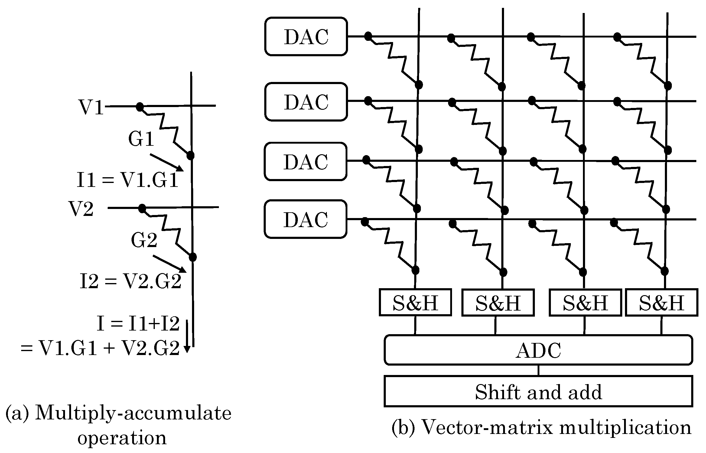
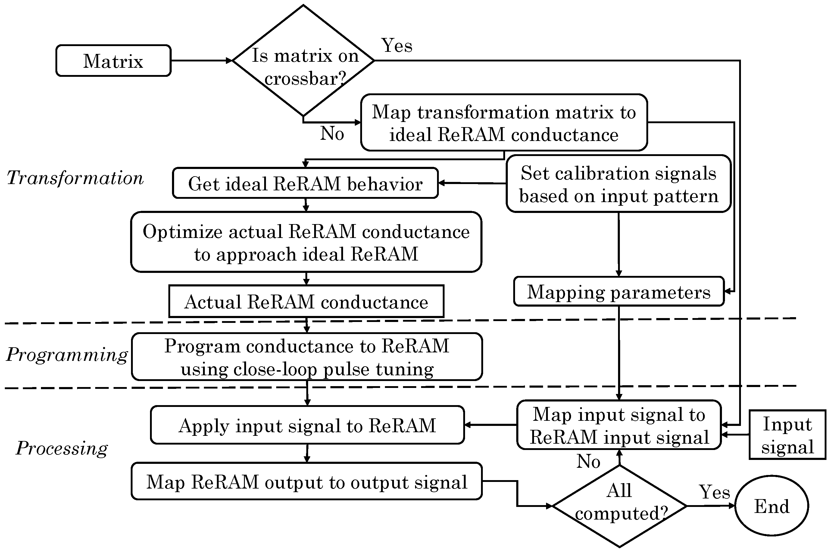
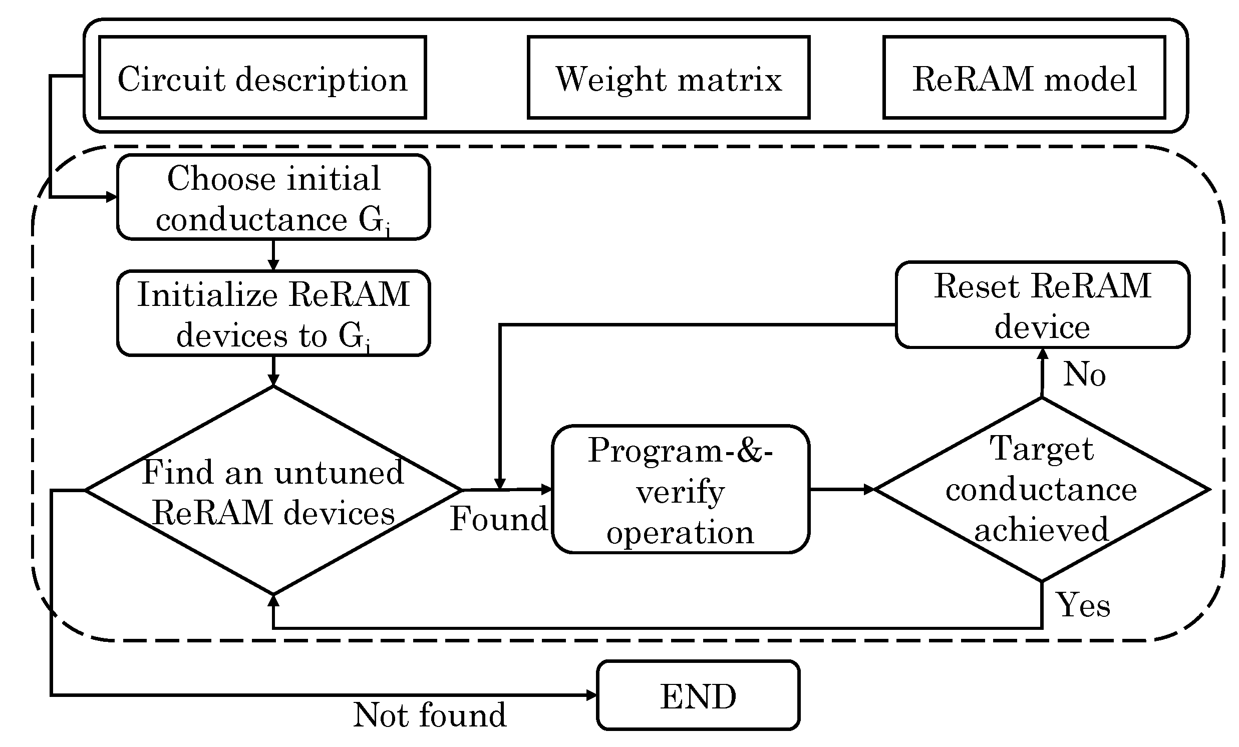
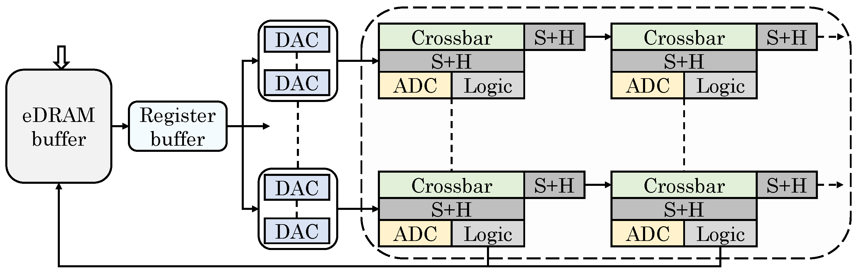
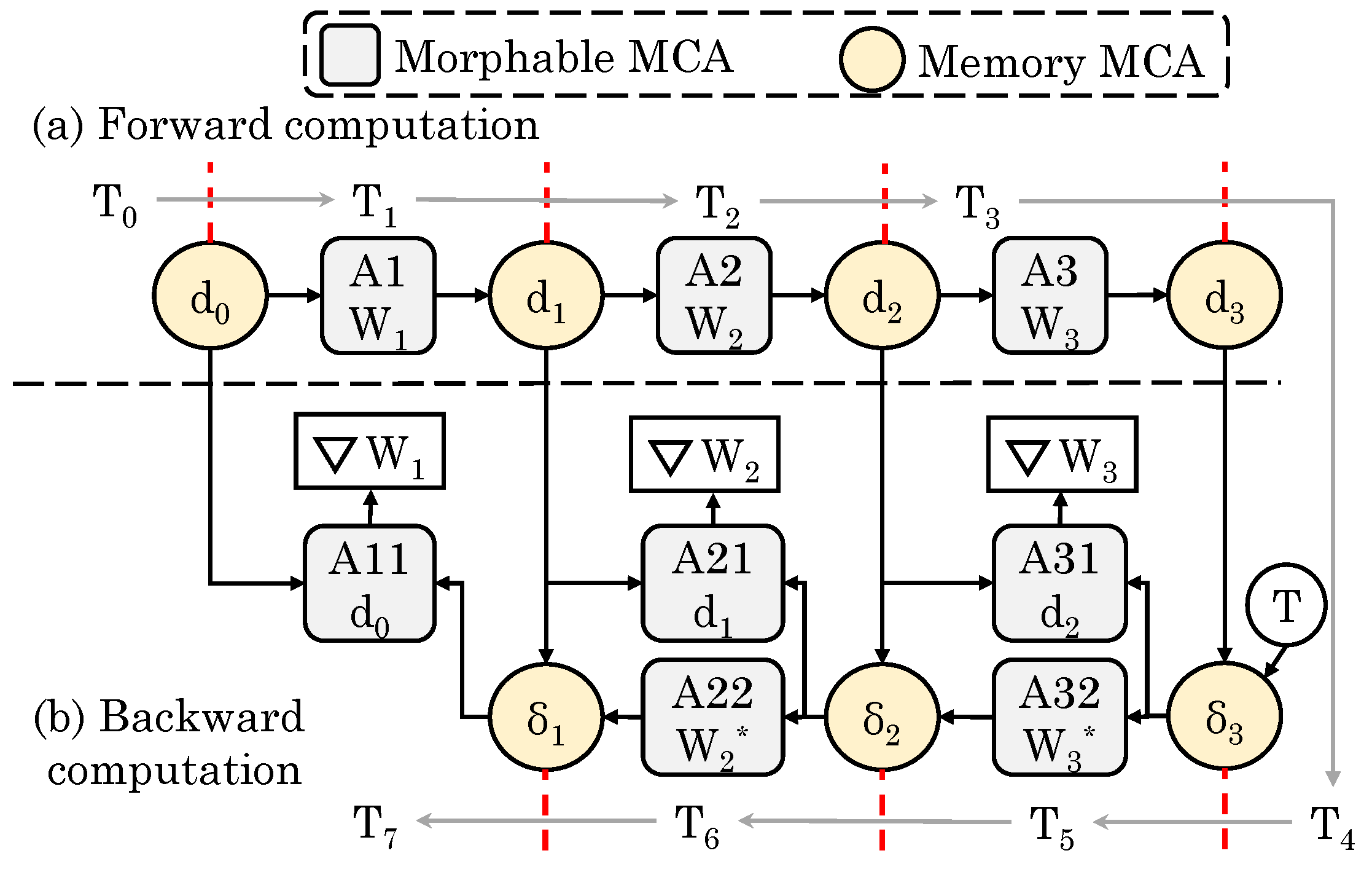
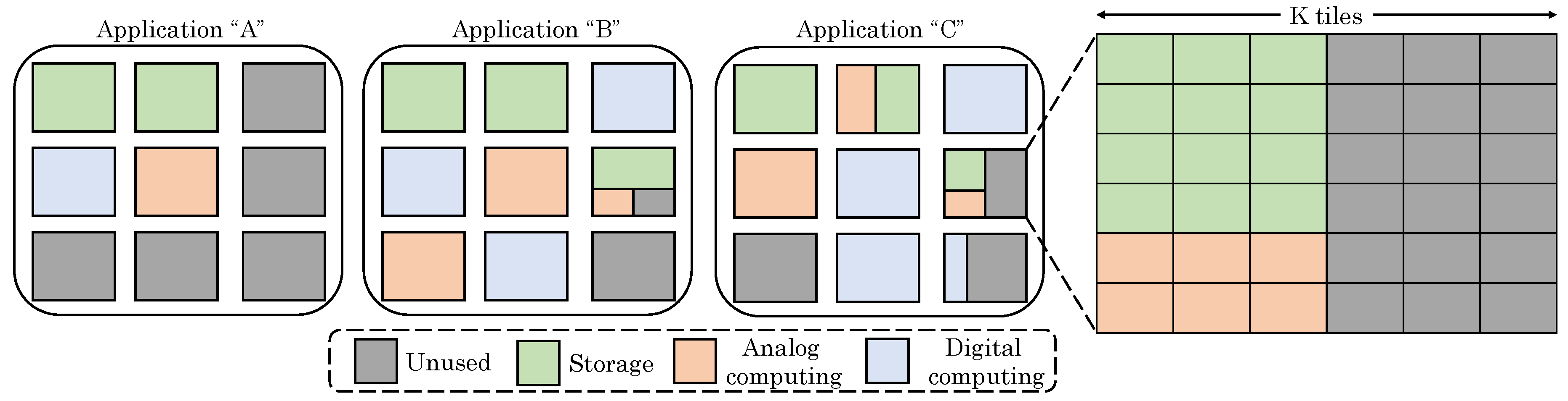
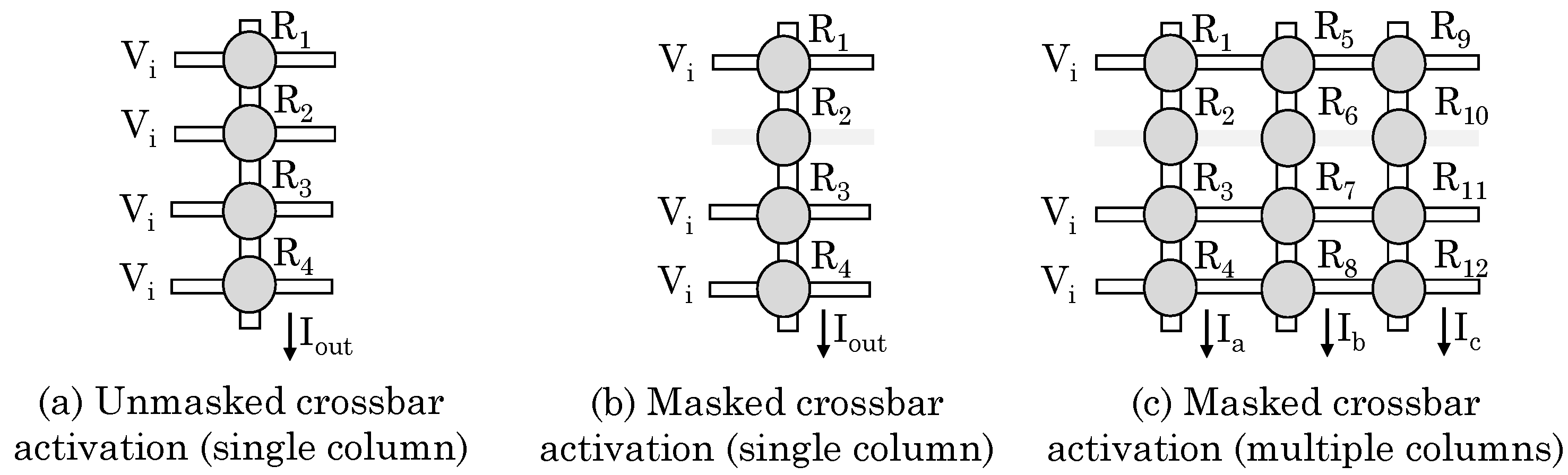
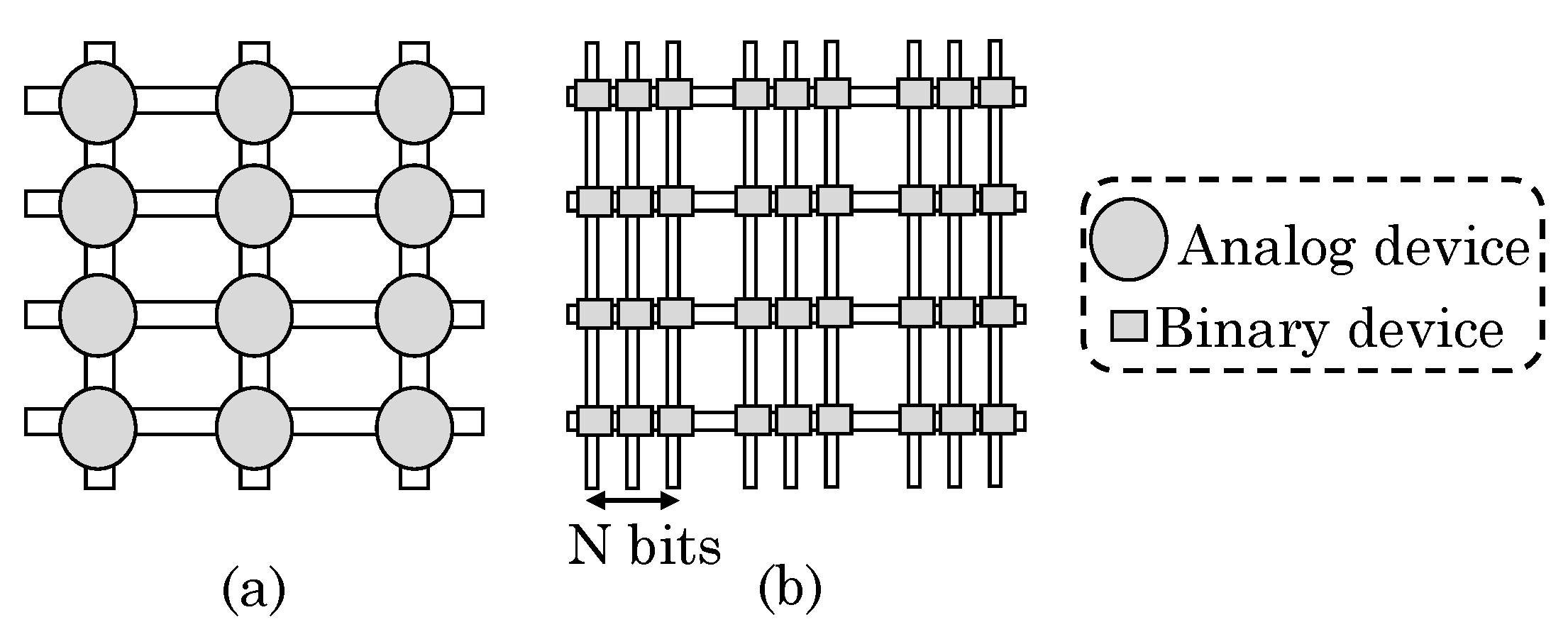
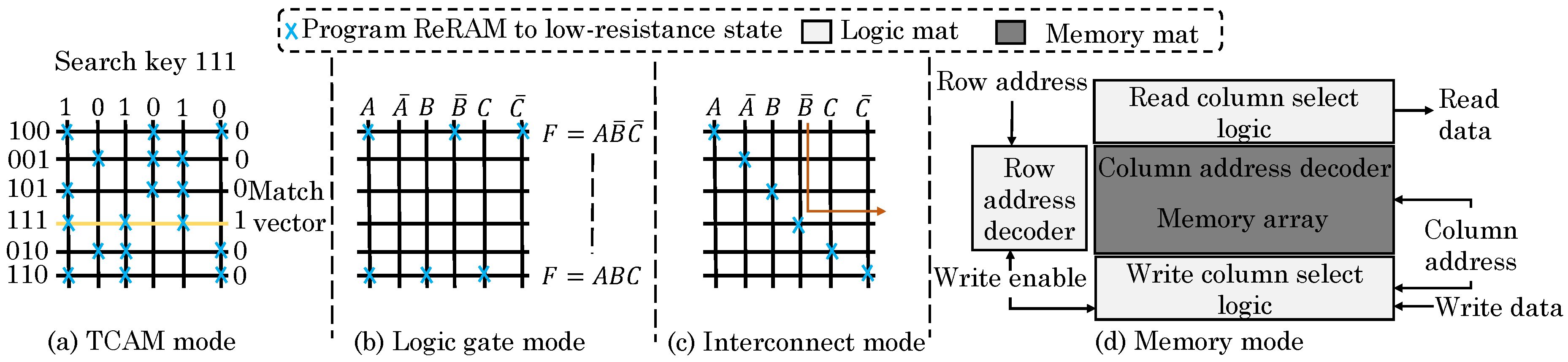
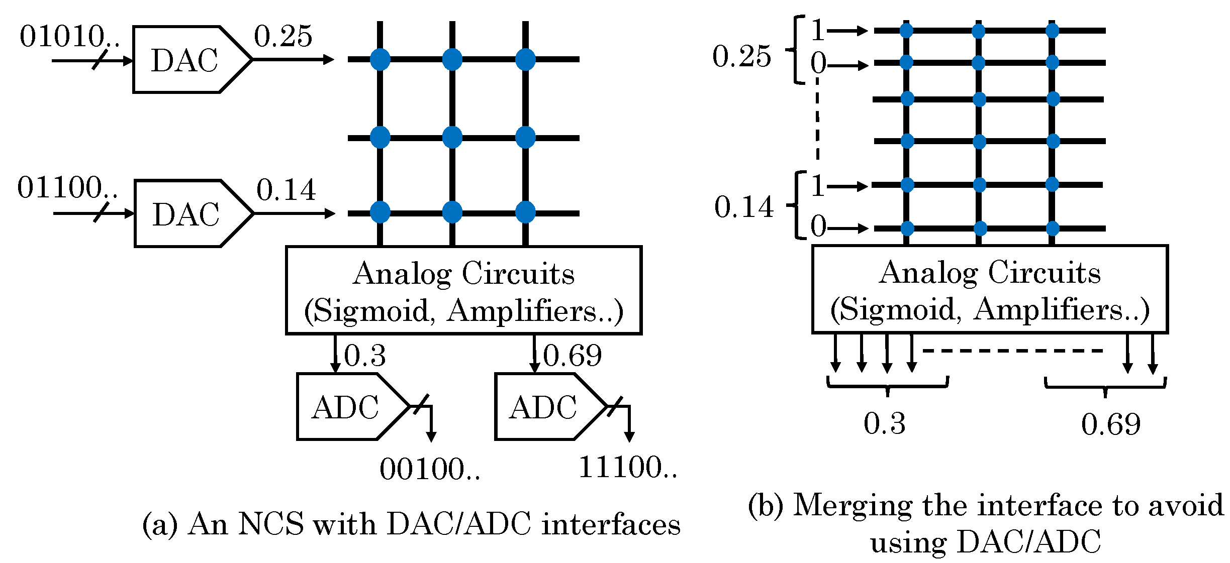
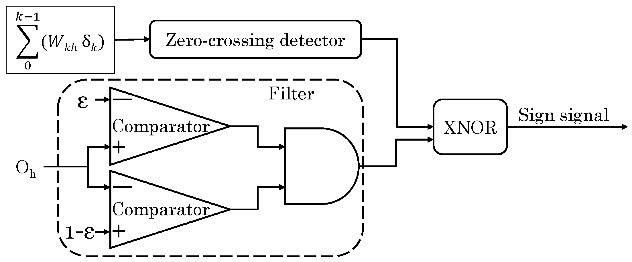
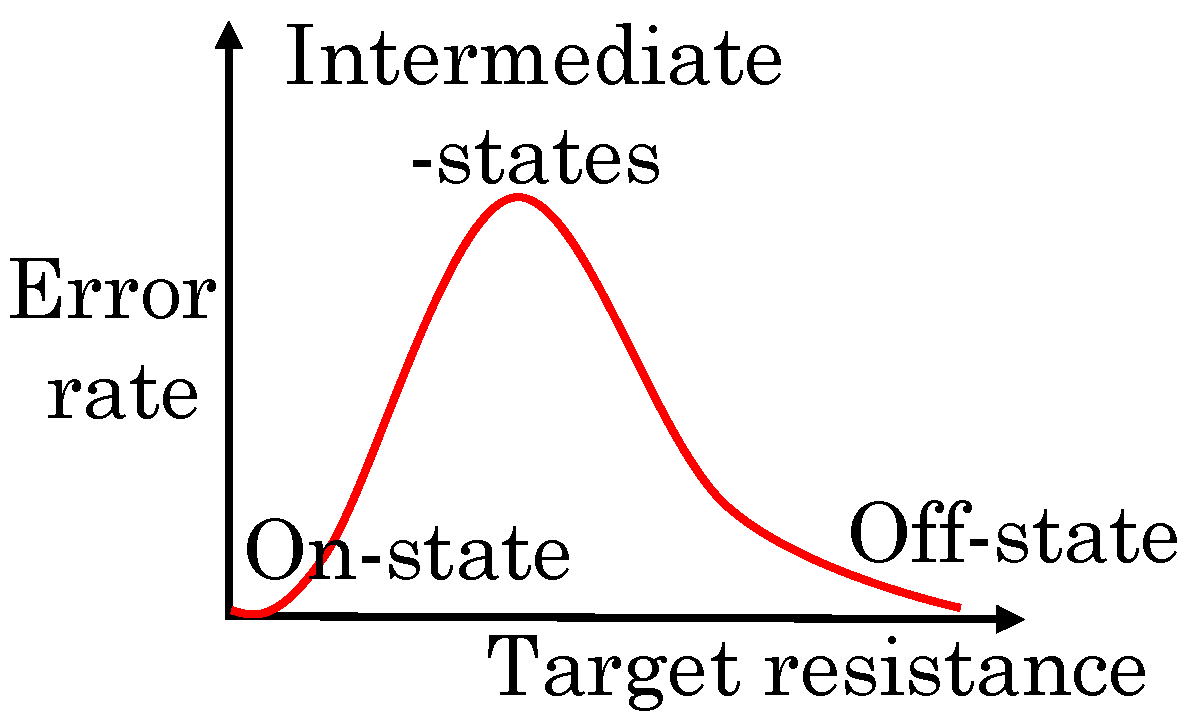
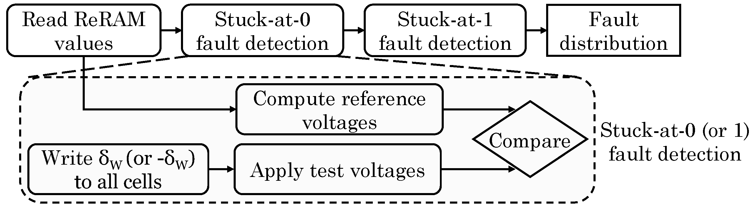
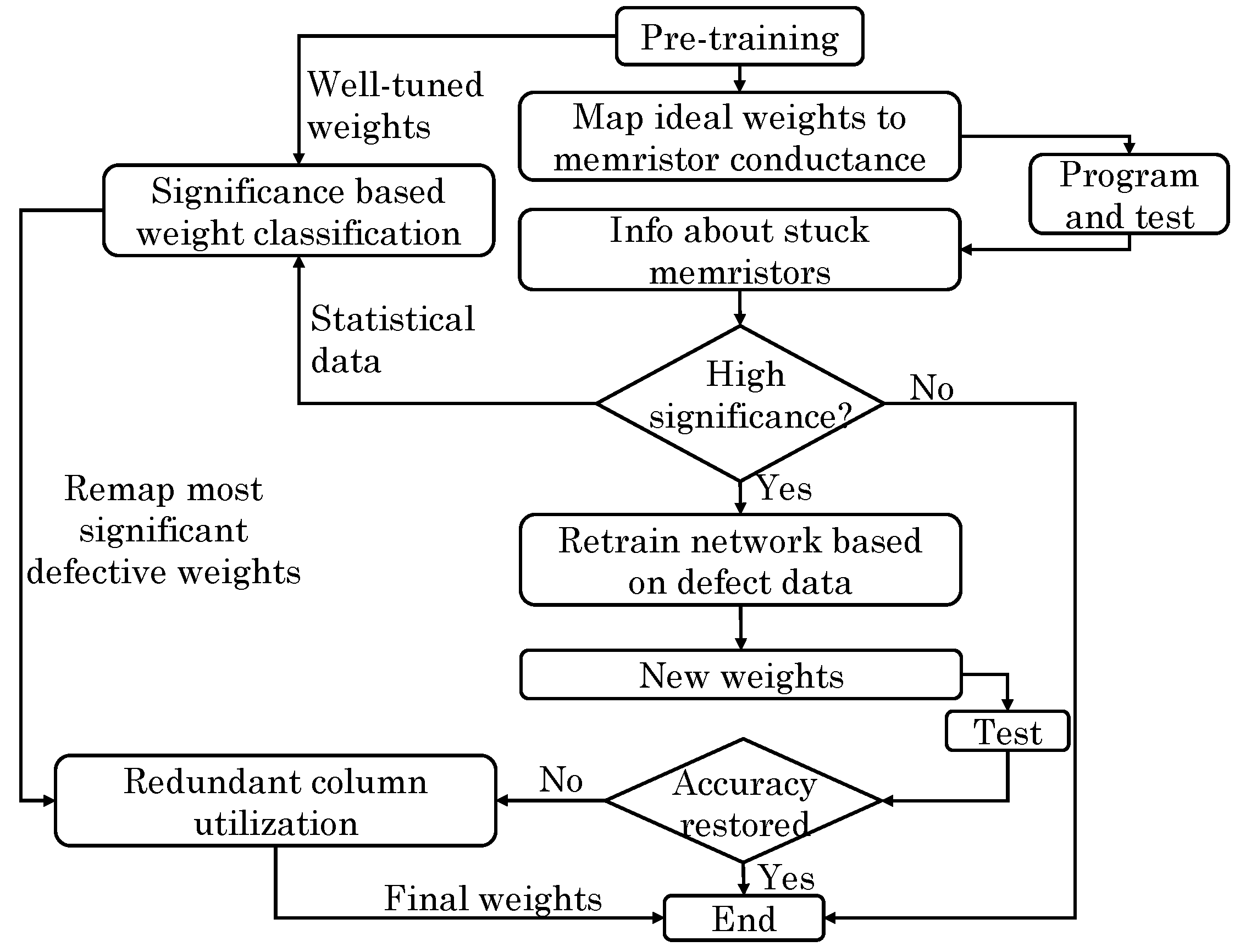
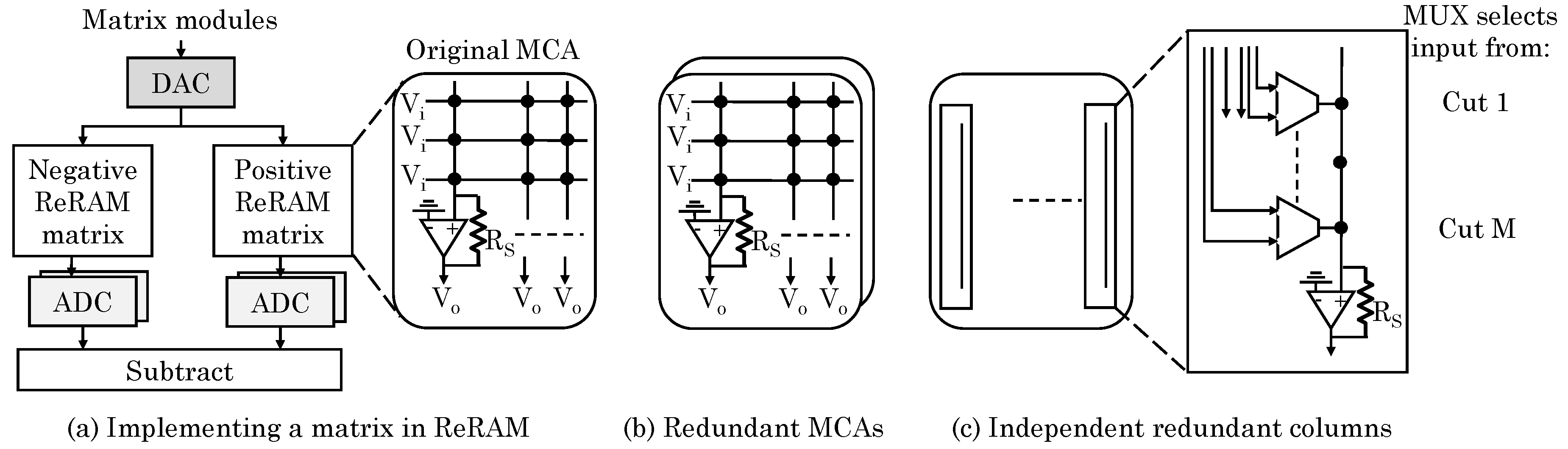
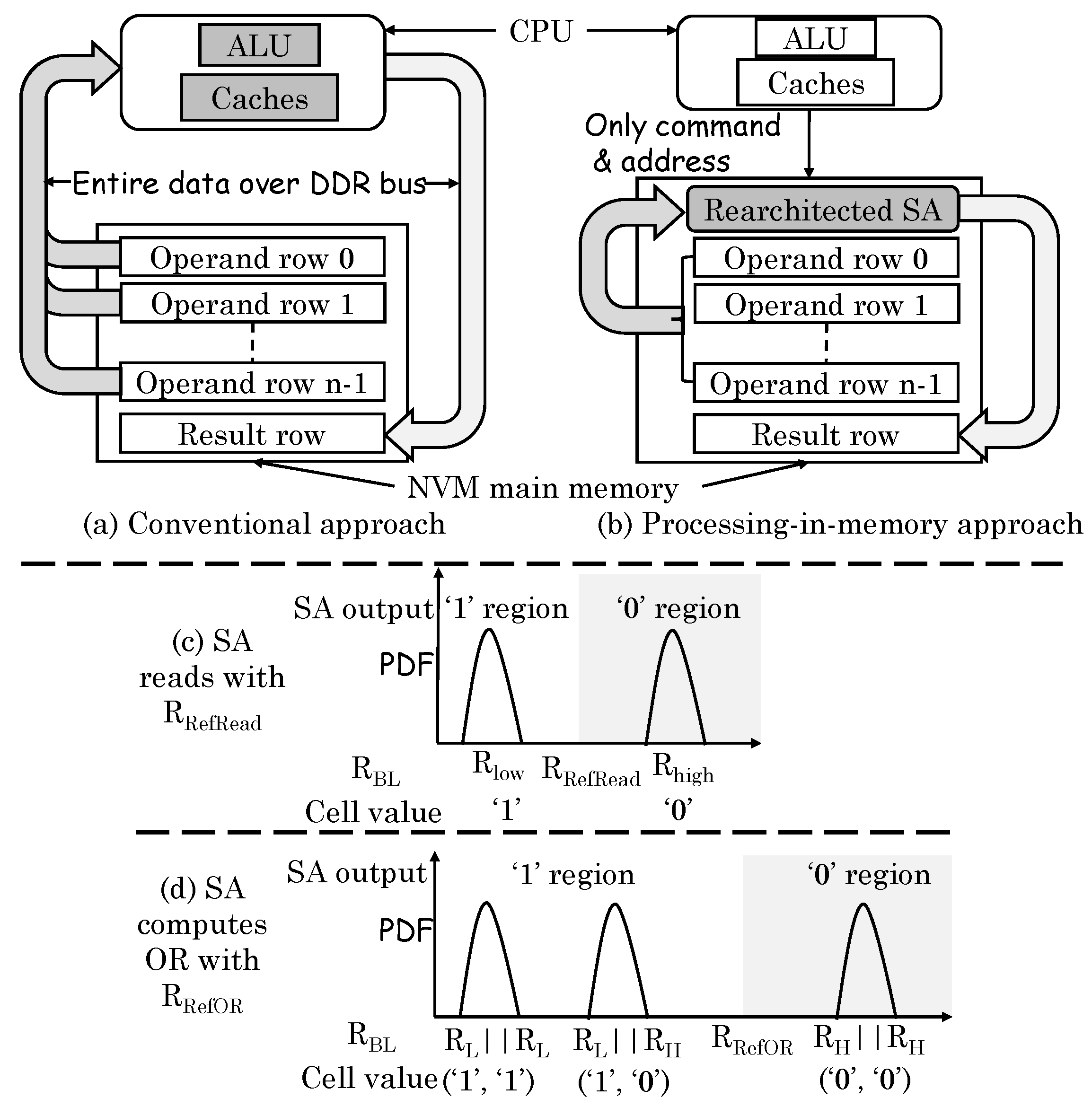
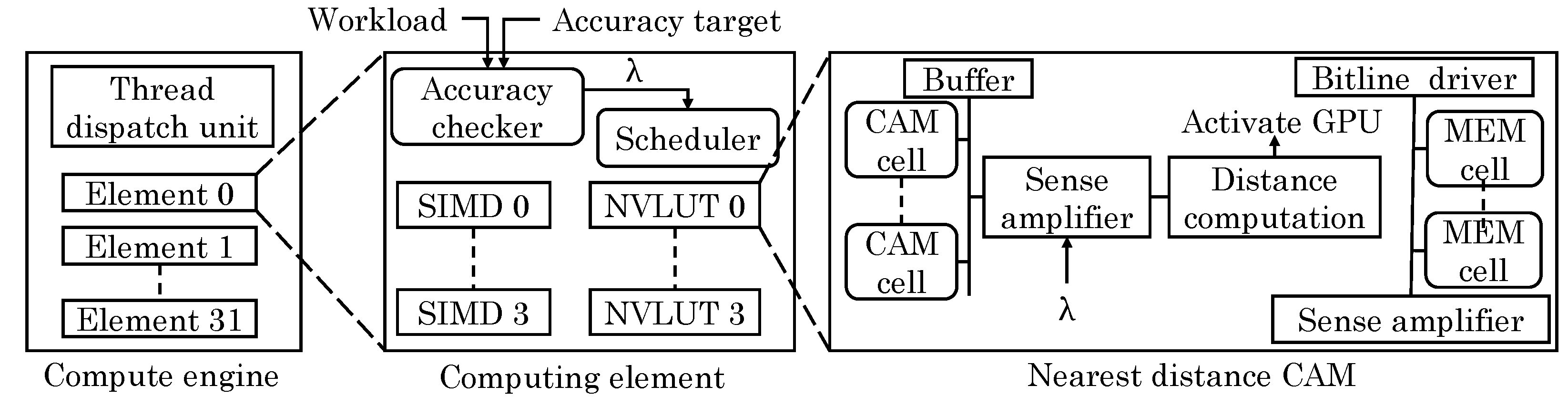
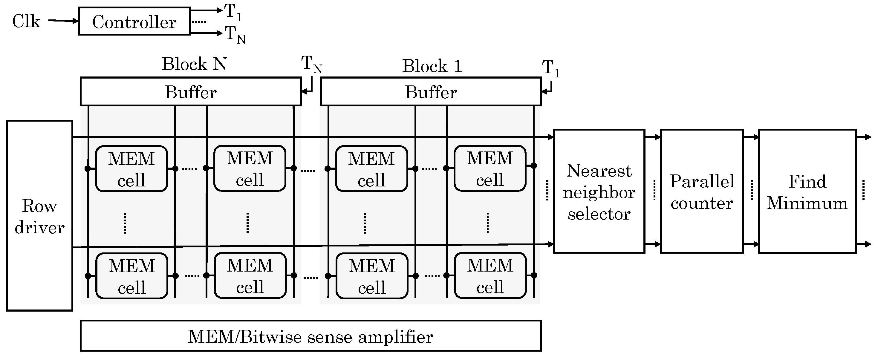
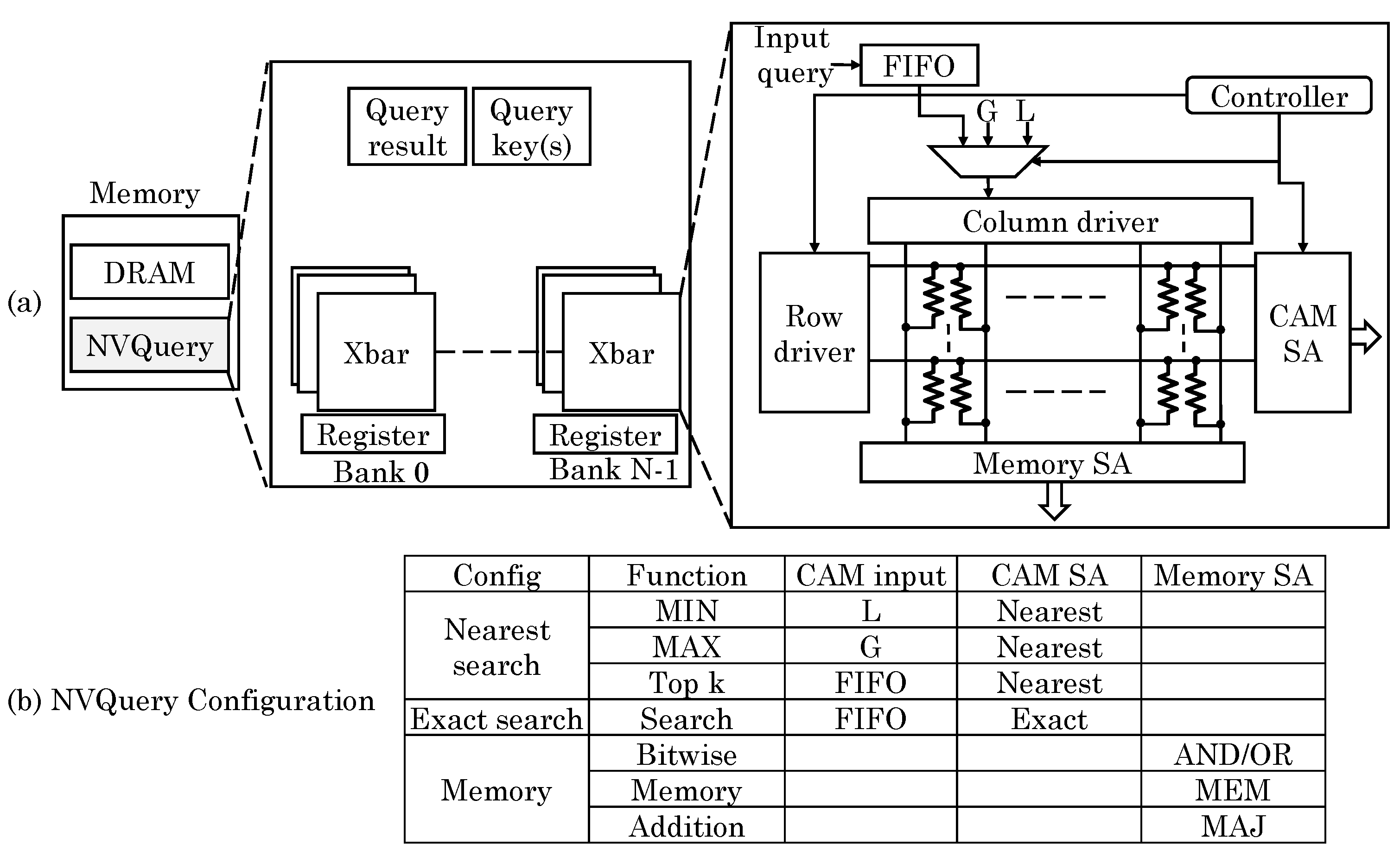
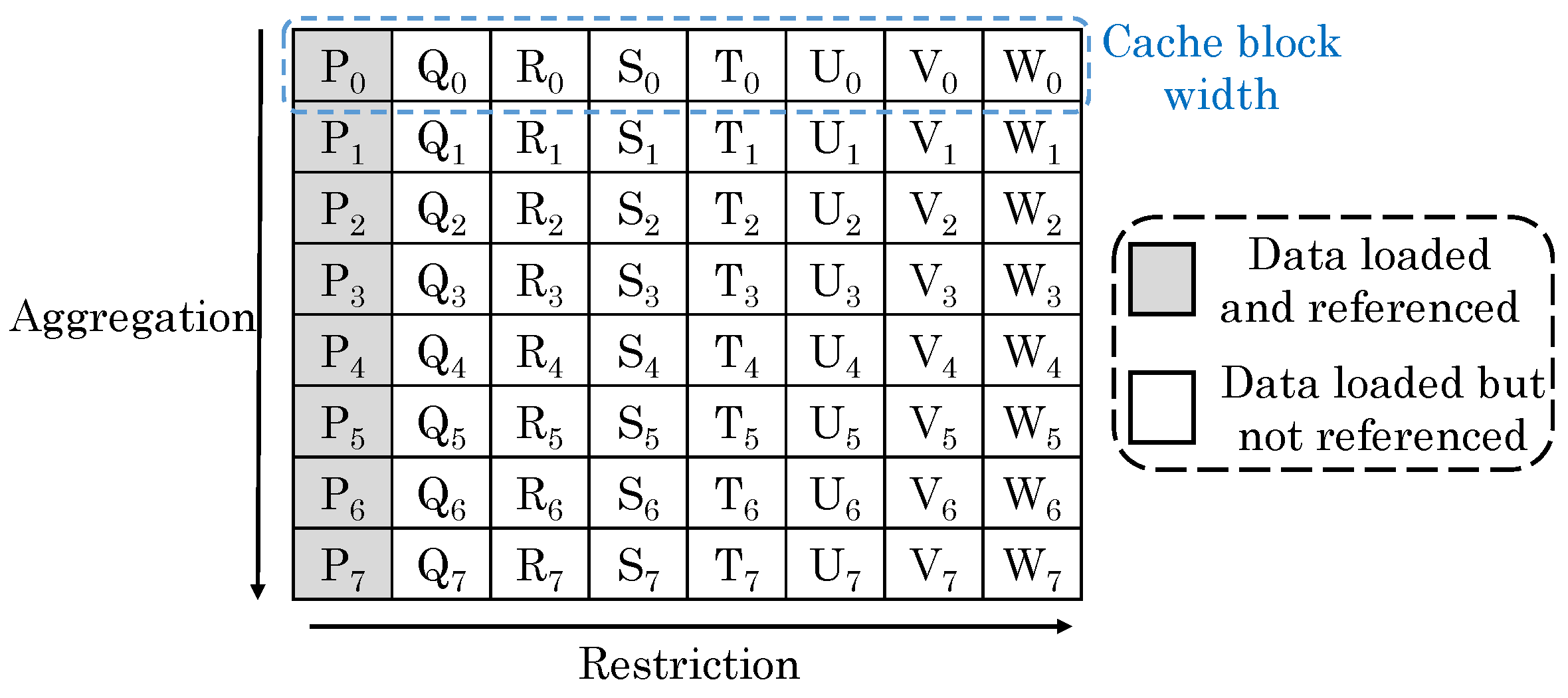
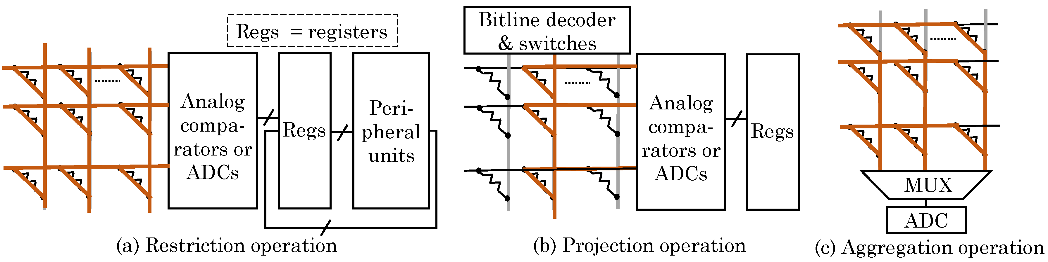
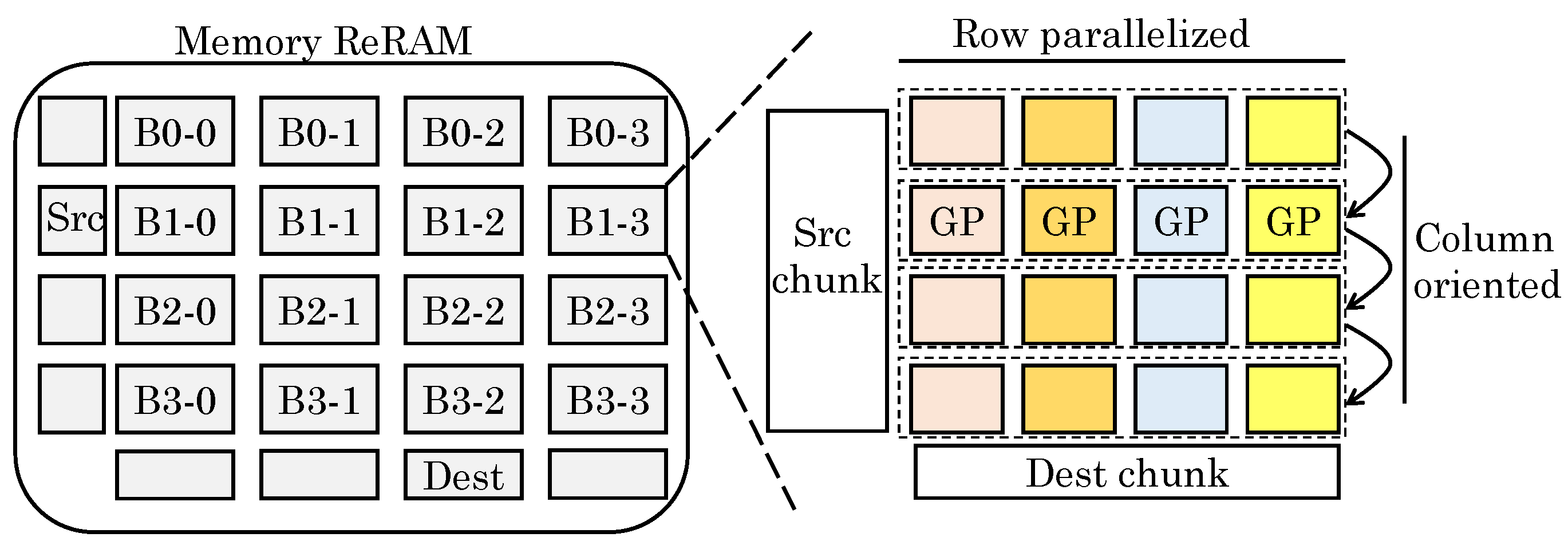
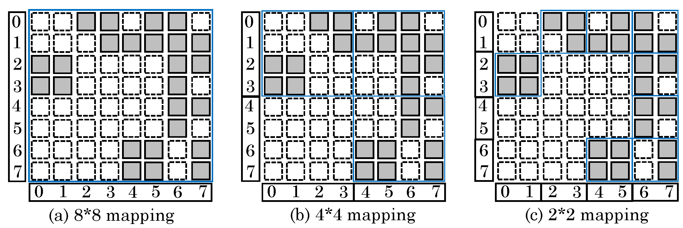
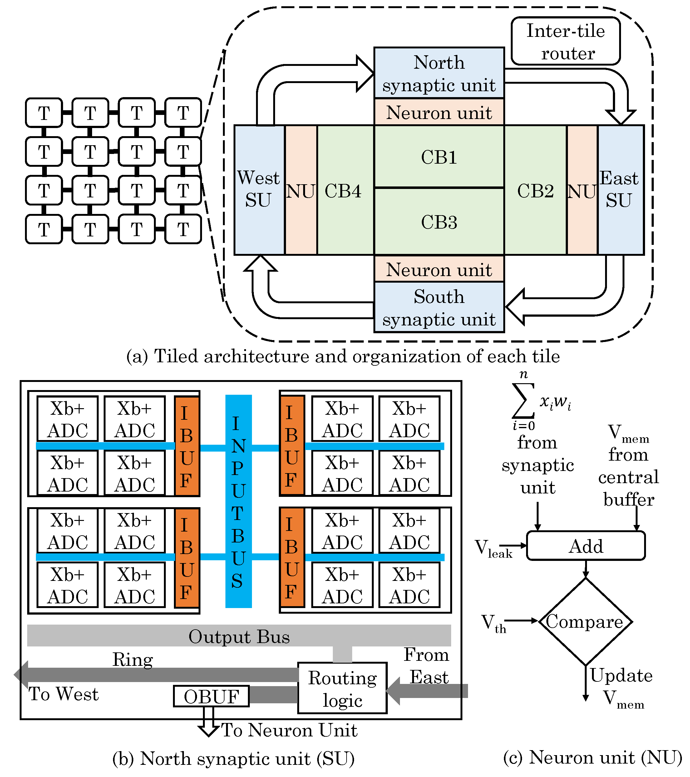
Table 1.
Classification based on NN architecture, optimization objective and comparative evaluation.
Table 1.
Classification based on NN architecture, optimization objective and comparative evaluation.
| Strategy | Reference |
|---|---|
| NN architecture | |
| Spiking NN | [15,44,45] |
| Artificial NN | nearly all others |
| Machine learning phase | |
| Training | [24,35,44,46,47] |
| Inference | nearly all |
| Optimization objective/approach | |
| Energy saving | [14,16,17,18,19,24,35,36,41,45,46,48,49,50,51,52,53,54,55,56,57,58,59,60,61] |
| Approximate computing | [20,35,43,62,63,64,65,66] |
| Pipelining | [16,17,19,46] |
| Pruning NN or exploiting NN sparsity | [19,20,67] |
| Binary architectures | binary NNs [41,61], performing binary BLAS operations [68] |
| Avoiding transfer of all-zero data packets | [15] |
| Storing multiple copies of data for achieving parallelism | [46] |
| Using eDRAM buffer to exploit data reuse | [16,17] |
| Algorithm | genetic algorithm [20], greedy algorithm [18,69], simulated, annealing [70], weighted bipartite-matching algorithm [47], graph clustering [67] |
| Comparison of ReRAM-based design with | |
| FPGA execution | [52,56,62,70] |
| GPU execution | [19,24,41,46,52,53,57,59,61,62] |
| CPU execution | [14,19,41,49,53,54,57,62,65,71,72] |
| ASIC design | [19,36,65,73] |
| SRAM-based design | [55,57] |
| DRAM-based design | [54] |
| Query-accelerator | [72] |
| TrueNorth | [41] |
| Design features | |
| Hybrid CMOS-ReRAM design | [19,68] |
| 3D design | [19,41] |
Table 2.
Strategies for mapping NN to ReRAM.
| Strategy | Reference |
|---|---|
| Storing positive and negative weights in different MCAs | [12,18,21,38,43,74] |
| Using only non-negative weights | [50] |
| Using multiple ReRAMs to overcome the precision limitation of ReRAM | [17,18] |
| Using tiled designs to avoid using large MCAs and/or to achieve fine-grain reconfigurability | [15,16,17,41,46,56,57,70] |
| Mapping largest weights to variation/fault-free MCAs to minimize errors | [69] |
| Assigning larger weights to MSB and smaller weights to LSB | [58] |
| Distinguishing between critical and non-critical weights | [37] |
| Avoiding costly SET operations in ReRAM | [24] |
Table 3.
Converting signed bitwise CONV to unsigned bitwise XNOR.
| a | w | (Multiplication) | A | W | (XNOR) |
|---|---|---|---|---|---|
| 1 | 1 | 1 | 1 | 1 | 1 |
| 1 | −1 | −1 | 1 | 0 | 0 |
| −1 | 1 | −1 | 0 | 1 | 0 |
| −1 | −1 | 1 | 0 | 0 | 1 |
Table 4.
Strategies for reducing overhead of analog implementation.
| Strategy | Reference |
|---|---|
| Avoiding/reducing the A/D converters | [17,44,46] |
| Reduce resolution (width) of converters | [16,17,57] |
| Using analog comparators to avoid using ADCs | [35,58,61,71] |
Table 5.
Domain of operation of different designs.
| Strategy | Reference |
|---|---|
| Digital-only design | [61] |
| Analog–digital hybrid design | [14,35] |
| Operating a tile in analog or digital domain | [41] |
| Analog design | nearly all others |
Table 6.
Reliability improvement techniques.
| Strategy | Reference |
|---|---|
| Issue addressed | |
| Process variation | [15,24,44,47,61,65] |
| Hard faults | [20,37,47,47] |
| Resistance drift | [75] |
| Signal distortion due to analog domain | [14] |
| Solution approach | |
| Redundancy scheme | [21,37] |
| Mapping zero weights to SA0 cells | [20] |
Table 7.
PIM approaches.
| Strategy | Reference |
|---|---|
| Bitwise/logical operations | [48,54,59,76] |
| Addition/MVM | [16,49,50,52,53,63] |
| Search operations | [52,59,64,65,71,72] |
Table 8.
XNOR truth table (adapted from [76]).
Table 8.
XNOR truth table (adapted from [76]).
| 0 | |||
| − | |||
| 0 |
Table 9.
Result of one-bit addition.
| Input | Output | |||
|---|---|---|---|---|
| 0 | 0 | 0 | 0 | 0 |
| 0 | 0 | 1 | 0 | 1 |
| 0 | 1 | 0 | 0 | 1 |
| 0 | 1 | 1 | 1 | 0 |
| 1 | 0 | 0 | 0 | 1 |
| 1 | 0 | 1 | 1 | 0 |
| 1 | 1 | 0 | 1 | 0 |
| 1 | 1 | 1 | 1 | 1 |
Table 10.
Approximate computing approaches.
| Strategy | Reference |
|---|---|
| Approximating mathematical functions | [62,63,66] |
| Approximating search operations | [64] |
| Precision-scaling or pruning | [17,20,35,65] |
| Quantization | [18,41] |
| Fixed-point operations | [16,43] |
| Performing more aggressive memresistance scaling in LSBs than in MSBs | [65] |
| Approximate storage | [43] |
| Additional retraining iterations to reduce the errors | [58,67] |
© 2018 by the author. Licensee MDPI, Basel, Switzerland. This article is an open access article distributed under the terms and conditions of the Creative Commons Attribution (CC BY) license (http://creativecommons.org/licenses/by/4.0/).
Share and Cite
MDPI and ACS Style
Mittal, S. A Survey of ReRAM-Based Architectures for Processing-In-Memory and Neural Networks. Mach. Learn. Knowl. Extr. 2019, 1, 75-114. https://0-doi-org.brum.beds.ac.uk/10.3390/make1010005
AMA Style
Mittal S. A Survey of ReRAM-Based Architectures for Processing-In-Memory and Neural Networks. Machine Learning and Knowledge Extraction. 2019; 1(1):75-114. https://0-doi-org.brum.beds.ac.uk/10.3390/make1010005
Chicago/Turabian StyleMittal, Sparsh. 2019. "A Survey of ReRAM-Based Architectures for Processing-In-Memory and Neural Networks" Machine Learning and Knowledge Extraction 1, no. 1: 75-114. https://0-doi-org.brum.beds.ac.uk/10.3390/make1010005