Study of a Synchronization System for Distributed Inverters Conceived for FPGA Devices


1
Department of Engineering and Architecture, University of Parma, Parco Area delle Scienze, 181/A, 43124 Parma, Italy
2
Department of Industrial Engineering, Alma Mater Studiorum University of Bologna, Viale del Risorgimento 2, 40136 Bologna, Italy
*
Authors to whom correspondence should be addressed.
Appl. Syst. Innov. 2021, 4(1), 5; https://0-doi-org.brum.beds.ac.uk/10.3390/asi4010005
Submission received: 1 December 2020
/
Revised: 7 January 2021
/
Accepted: 12 January 2021
/
Published: 15 January 2021
(This article belongs to the Special Issue Smart Grids and Contemporary Electricity Markets)
Abstract
:In a multiple parallel-connected inverters system, limiting the circulating current phenomenon is mandatory since it may influence efficiency and reliability. In this paper, a new control method aimed at this purpose and conceived to be implemented on a Field Programmable Gate Array (FPGA) device is presented. Each of the inverters, connected in parallel, is conceived to be equipped with an FPGA that controls the Pulse-Width Modulation (PWM) waveform without intercommunication with the others. The hardware implemented is the same for every inverter; therefore, the addition of a new module does not require redesign, enhancing system modularity. The system has been simulated in a Simulink environment. To study its behavior and to improve the control method, simulations with two parallel-connected inverters have been firstly conducted, then additional simulations have been performed with increasing complexity to demonstrate the quality of the algorithm. The results prove the ability of the method proposed to limit the circulating currents to negligible values.
1. Introduction
In recent years, smart grids have become a very important topic and are extensively debated in the literature [1]. A smart grid is a network that can efficaciously monitor and manage the transport of electricity produced by generators to meet the varying electricity demands of end-users [2,3]. To add intelligence to a smart grid, the network must integrate signal processing blocks and communication logic. Conventionally, methods such as the use of parallel capacitors, tap-changing transformers and SVC (Static Var Compensator) are adopted [4]. These power controls generally lack precision and do not work in real time; to overcome these limitations, different solutions relying on FPGA (Field Programmable Gate Array)-implemented algorithms can be exploited [5]. In the last few years, the application of FPGA devices has increased exponentially in a wide variety of fields, such as: digital signal processing [6,7,8,9,10], data processing [11,12], bioinformatics [13,14] and power electronics [15,16,17]. Among the applications based on FPGAs that recently have been applied to the smart grid field, MPC (Model Predictive Control) has particular importance [18,19,20]. An MPC is a control strategy that allows predicting the output of a discrete-time model, combining the input data and the current state of the model to choose the optimal control action. Implementing the complicated and challenging algorithms on FPGA devices can help to minimize the real-time response. Moreover, exploiting FPGAs in this context can lead to a strong advantage in terms of flexibility, reliability and costs [1,20]. In [20], an example of FPGA application is presented and, specifically, the strategy of voltage control in a smart grid is proposed.
The FPGAs are also used in converters and, in particular, in inverter-based applications, such as switching control, voltage balance and fault detection [16]. An inverter is a DC/AC converter that transforms a DC input voltage into a symmetrical AC output voltage. The field of inverter applications has been widely investigated: solutions where inverters are connected in parallel to form a microgrid (a kind of small-scale grid that contains distributed generators of various natures) have been proposed in the literature [21,22,23]. The parallel connection of inverters improves redundancy and then reliability, but it is very sensitive and complicated because each module must have the same output voltage as the others. Not respecting this requirement leads to crosscurrent or circulating current between the inverters with the effect of reducing power efficiency and system reliability. The circulating current behavior in multiparallel connected inverters has been widely discussed in [24,25,26,27]. In [24], the authors studied the effect of this current in a system with two inverters and in a more general case of N inverters. In both cases, they reported that the phenomenon exists if there is a difference in the output voltage phase or frequency. The authors also concluded that the circulating current is independent of the load, that is, a current superimposed on the normal current and, finally, that can cause power exchange among the inverters connected (in the case of a no load or low-load condition). In [25], an active rejection control based on a Reduced-order Extended State Observer (RESO) is reported. The scheme proposed reduces the mutual currents with a less model-dependent control design.
In [28], the authors studied the circulating current phenomenon, mentioning control methods such as droop control, master–slave control, instantaneous current sharing control and parallelism control. The droop-control method allows one to regulate the frequency and the amplitude of the inverter output voltage by adjusting the active and reactive-power flow through a linear dependence. In particular, the frequency can be used to control the active-power flow, while the amplitude of the output voltage to control the reactive-power flow [21]. In [29], the authors discussed a different approach of the droop control for parallel-connected inverters based on active and reactive currents: handling active and reactive current instead of active and reactive power has the advantage that, in case of short circuiting, the control of active and reactive currents avoids the risk of an infinite current due to any non-zero active or reactive powers. Another example of application can be found in [30], in which the authors use a dynamic phasor-based model and a SOGI-FLL (Second-Order Generalized Integrator Frequency-Locked-Loop) to implement a droop-controlled parallel-connected inverter system. The master–slave control is composed of a master inverter that operates in a voltage-controlled mode while all the other inverters, the slaves, operate in a current-controlled mode. In [31], a master–slave application with a wireless communication and current sharing control among the inverters is described: it is a centralized technique in which all the inverters share information about the current shared among them. In [32], the parallelism control is applied to a UPS-based system. In [33], the authors analyzed a method to suppress the cross-circulating current based on virtual impedance. In [34], the authors presented a new wireless load-sharing control method that is designed to improve the performances of the parallel-connected inverters. They also defined the circulating current and proposed an adaptive droop-control method. Another type of control is presented and discussed in [35]; the authors realized a system controlled by local hardware managers and a central application manager connected with an optical fiber.
Some approaches based on FPGA devices have also been studied: in [36], a controller developed on DSP (Digital Signal Processor) and FPGA for paralleling multiple inverters is presented. The controller is shared among the units and a synchronization scheme exploiting UPP (Universal Parallel Port) protocol is introduced to eliminate the synchronization delay. Moreover, in [37], an FPGA innovative control is proposed. The presented approach does not require communication among units, and it is applied to a system with only two parallel inverters.
In this paper, a new approach to solve the several inverters parallelism problems and minimize the circulating current is presented. A new control method has been studied with the main purpose of controlling the system without any type of communication among the inverters and without introducing other structures such as a PID controller, as is typically described in literature [21,34,35]. For this purpose, the advantages of FPGA devices have been exploited: while conventional controllers operate sequentially, FPGAs are parallel processing devices, allowing the execution of complicated tasks in reduced time. Moreover, the FPGA hardware structure is not fixed, but can be reprogrammed by the user, adapting it to the application. In this scenario, FPGAs only control their own inverter and do not care about the operation mode of the other inverters (that can be operative or not) connected to the network. The proposed control method exploits high FPGA clock frequency to react to the circulating current as fast as possible. This feature allows for limitation of the circulating current peaks to prevent the damage of the devices. Moreover, the absence of communication between the inverters reduces the system complexity and costs, avoiding the realization of a dedicated communication line and protocol. The proposed control method permits one to realize scalable systems where modules, each one including an FPGA and an inverter, can be simply connected or disconnected to the system.
The system has been developed and simulated with a model-based design approach compliant with automatic code generation. Exploiting these techniques allows one to reduce the time-to-market and, above all, guarantees greater portability of the system since the design process is vendor-independent and, in the exporting phase, it is possible to select different types of FPGAs.
2. Materials and Methods
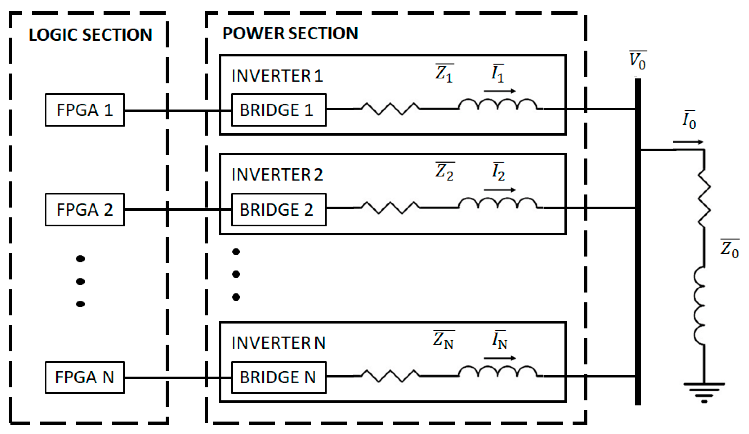
The system proposed is composed by N inverters connected in parallel as shown in Figure 1. The power section is based on the equivalent model presented in [38]. , and are the output currents of the inverters, , and are the impedances of the units, is the load impedance and is the load voltage. Each inverter module has its control logic (FPGA) and a BRIDGE module to convert the FPGA signal (0–3.3 V) to the output voltage (±300 V).
The parallel connection of singular units could generate a circulating current that flows towards the inverters, due to the attempt to impose different voltages on the same output. To limit this current, a suitable control method, to be implemented on every single FPGA module, is proposed, to synchronize the inverter outputs. Comparators, implemented on the FPGAs, are introduced to detect if the module output current assumes values out of a predetermined range. If this situation occurs, an FPGA reset signal brings back to the ordinary operation by modifying the Pulse-Width Modulation (PWM) signal controlling the BRIDGE. The method just described implies the absence of intercommunication between the inverters differently from what has been seen in the literature, allowing the design of a scalable and easier system.
Initially, to prove the validity of the approach, a simple structure with two inverters connected in parallel has been considered.
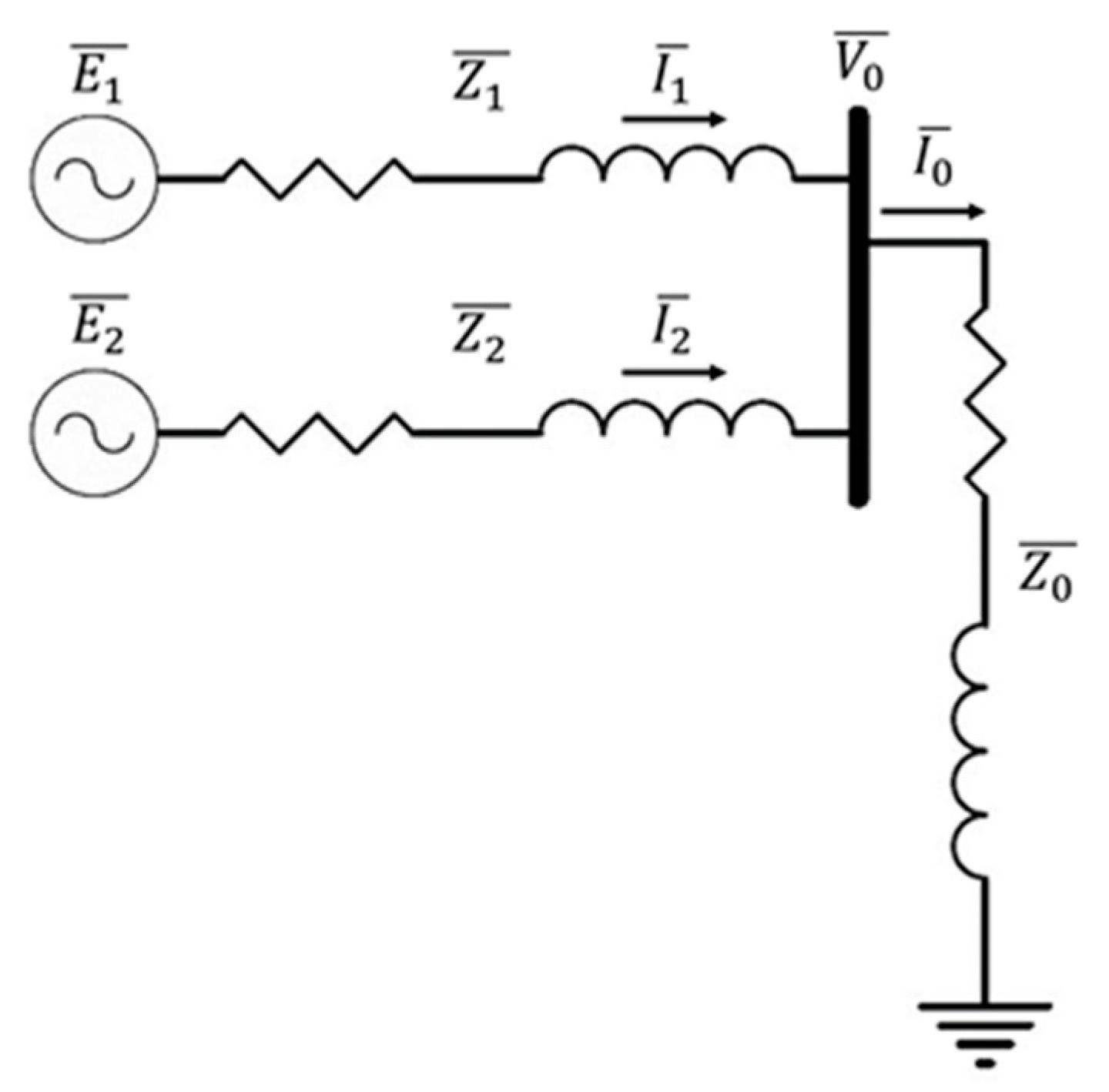
The schematic of this structure is depicted in Figure 2. and are, respectively, the output voltages of the first inverter and the second inverter. As described in Figure 1, and are the impedances of the modules, is the load impedance, is the load current and the load voltage. The simulated system includes 10 kW inverters, a 600 V DC-link and a PWM at frequency of 50 kHz. A unit line impedance with an inductive part of 250 nH and a resistive part of 1 mΩ has been considered, together with an inductive load of a 1 mH in series with a resistance of 1 mΩ. In this paper, a Simulink model conceived to be exported via a Hardware Description Language (HDL) coder to a vendor-independent code has been designed. A 100 MHz system clock frequency, usually implemented on medium-level FPGA boards (e.g., Xilinx Artix-7 XC7A100T FPGA), has been considered. After the simulation of the system composed of two inverters, a second set of simulations has been considered, extending the approach to a greater number of parallel-connected inverters. MATLAB and Simulink with Simscape and Stateflow add-ons have been used to simulate the system behavior and to develop the new control idea. MATLAB is a powerful tool that allows multidomain simulation, thanks to a vast variety of available tools. Simulink is a MATLAB-based graphical programming environment that is widely used for model-based design. In this work, Simulink has been utilized with Simscape, a MATLAB add-on employed to create models of physical systems. Specifically, Simscape Electrical provides component libraries for modelling and simulating electronic, mechatronics and electrical power systems. Stateflow is another important tool that is able to design and simulate Finite State Machine (FSM) and logical flowchart. All the MATLAB functions, Simulink models and Stateflow charts used in this work are compatible with HDL Coder (Hardware Description Language Coder), which allows for converting models in synthesizable VHDL and Verilog code automatically on an FPGA.
In order to understand how the system reacts to anomalies in Pulse-Width Modulation (PWM) signals, the two parallel-connected inverters system without any control logic has been firstly simulated with varying PWM frequencies, phases and duty cycles. Then, the new control method, based on the Finite State Machine (FSM) algorithm, has been applied, controlling the current of each module of the network, starting from a steady-state condition, with the FPGAs that manage a smart reset logic to automatically start the PWM signals on the basis of measured circulating current. The extension of the developed algorithm to the N-inverter case has been then introduced to test the generalization capability.
2.1. Circulating Current Phenomenon
The circulating current has been defined as the difference between the output current of each inverter and the average current (that is the sum of the outputs current divided by the number of inverters) [24]:
where I1 and I2 are the output currents of the first and the second inverter, Iavg is the average output current, IH1 and IH2 are the circulating currents seen by the first inverter and by the second inverter, respectively. All the currents are expressed in Ampère.
The discussion so far can be generalized in the case of N inverters. Similar to what has been performed previously, the current seen by each inverter can be calculated as:
where k is the number of the inverter considered, Ek is the output voltage of the k-th inverter and V0 the load voltage, both expressed in Volt. Zk is the load impedance in Ohm. The average output current, then, is defined as:
where Ij is the output current of the j-th inverter and N is the number of inverters.
Finally, the circulating current seen by an inverter in a system with N parallel-connected inverters can be calculated as the difference of its own output current and the average current:
where k is the inverter number, N is the total number of inverters and is the circulating current seen by the k-th inverter expressed in Ampère.
2.2. Designed System
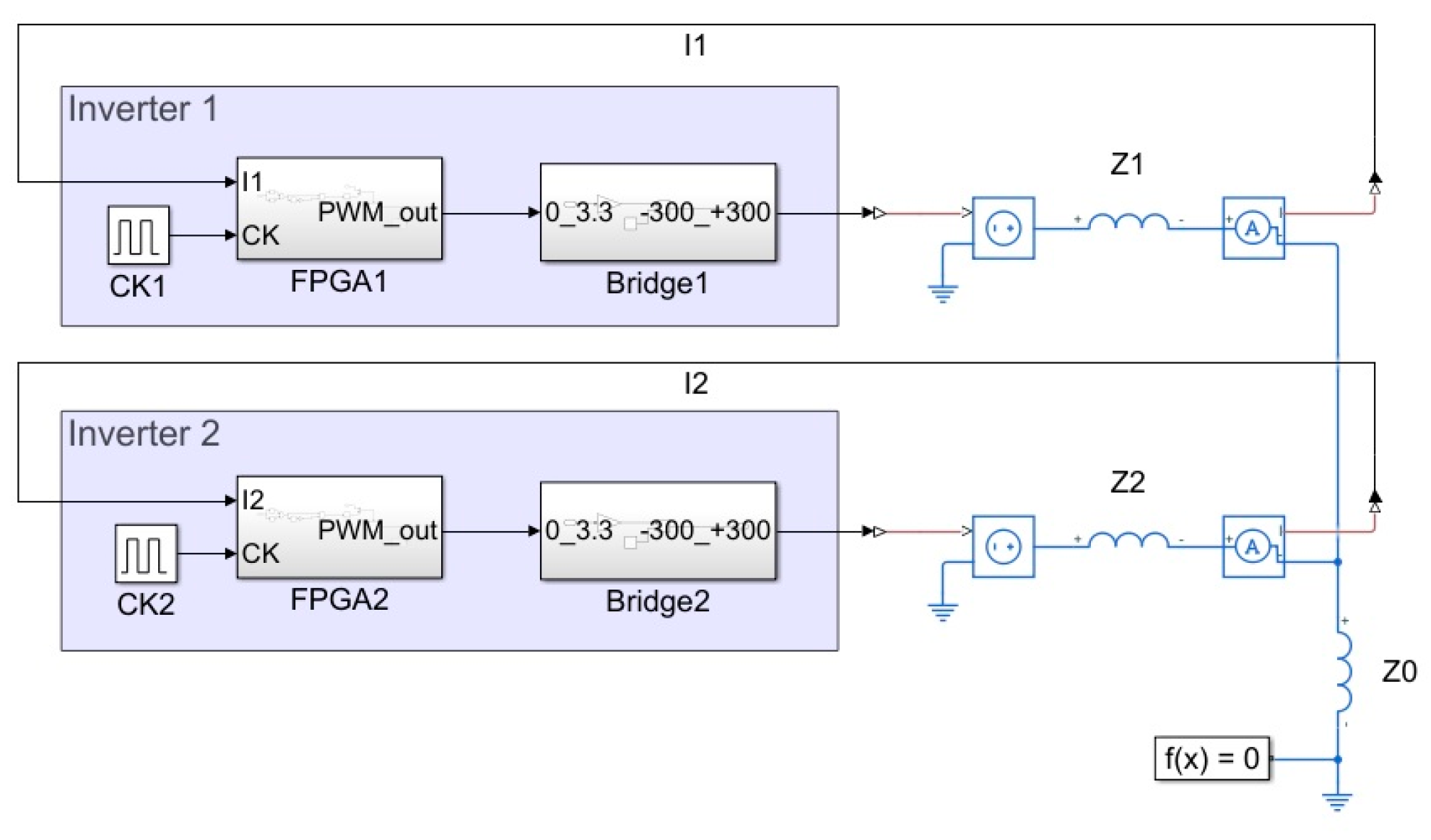
The system described before has been simulated in Simulink. Figure 3 is an example of a model-based system designed for N = 2.
In this case, the impedance lines, Z1 and Z2, are equal with a resistive part of 1 mΩ and an inductive part of 250 nH. They represent the non-ideality of the cables used to connect the inverters to the load, while Z0 is the load impedance composed of a resistive part of 1 mΩ and an inductive part of 1 mH. The subsystems, FPGA1 and FPGA2, contain the core of the simulation model: the FSM that controls the PWM and its reset logical rules. The subsystems, BRIDGE1 and BRIDGE2, are the modules dedicated to converting the FPGA signal (0–3.3 V) to the output voltage (±300 V). Indeed, the inverter module is composed of a logical section (FPGA device), with a power supply of 3.3 V, and a power section that provides the ±300 V output voltage. A load current operating point of 10 A has been imposed, that means a current of 5 A in each module for the two-inverters system.
To take into account crystal oscillator tolerance or possible non-perfect synchronization in the switch on of the inverters, which could lead to the generation of circulating currents, different phase and frequency clocks have been considered. As an example, in the two parallel-connected inverters system depicted in Figure 3, the clock of the first inverter was imposed to 100 MHz, while in the second inverter a clock frequency 0.1% greater and a 5 ns clock phase delay were forced. Crystal oscillator datasheets that are generally used in FPGA applications are reported in [39,40]. The frequency variation estimated is around 10 ppm and 100 ppm. Hence, to demonstrate the validity of the approach and to take into account the ageing of the crystal oscillator, a tolerance of 1000 ppm (corresponding to 0.1%) has been considered.
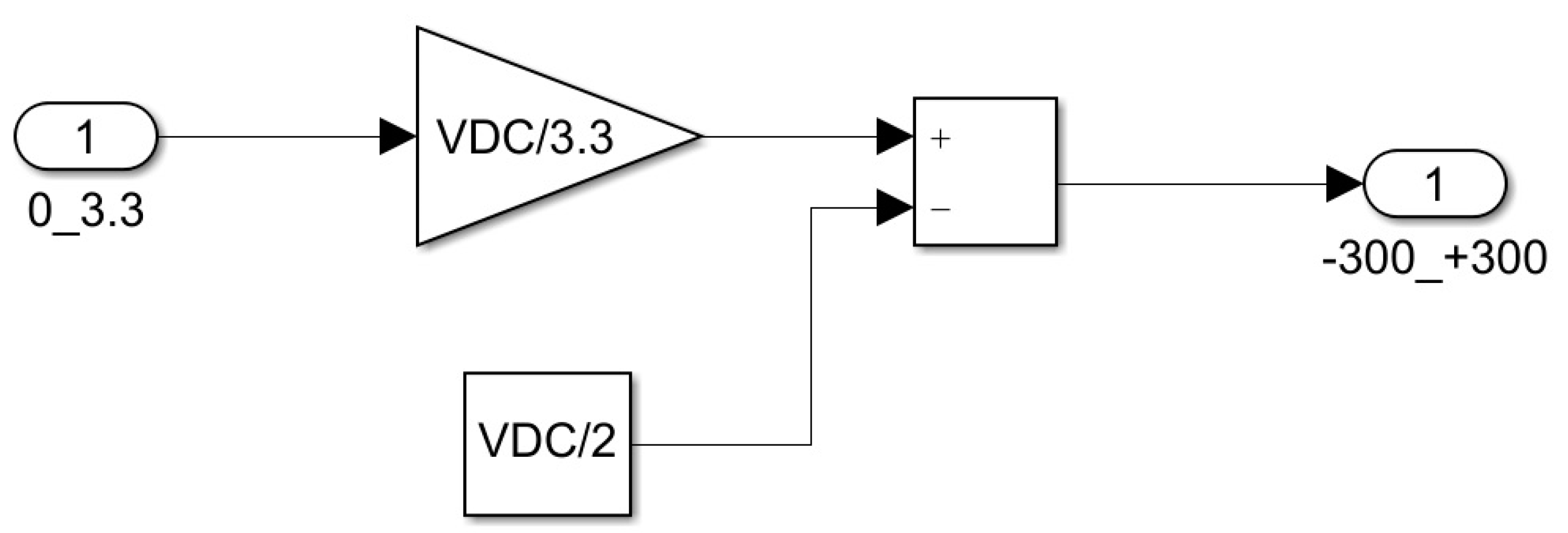
In Figure 4, the subsystems BRIDGE is presented. All the subsystems deployed in the main model-based schematic with the same function are perfectly identical.
The subsystem BRIDGE aims to convert the FPGA-output control signals into power system signals. In this paper, the internal architecture of the inverter has not been studied because the effort has been concentrated on its control regardless of its internal structure. The Simulink model represents the BRIDGE inverter controlled by a 0–3.3 V signal. The low-pass filter, employed to convert the square wave into the output sine wave, which is normally required after the inverter, has not been considered, since it does not affect the simulation results. VDC is the constant DC-link equal to 600 V. The conversion is achieved with the simple Equation (6):
where Vout is the output voltage of the BRIDGE and VDC is the voltage of the system DC-link, both expressed in Volt.
The FPGA subsystem includes the model-based design of the proposed new control method that is described in detail in the following paragraph.
2.3. The Proposed Control Method
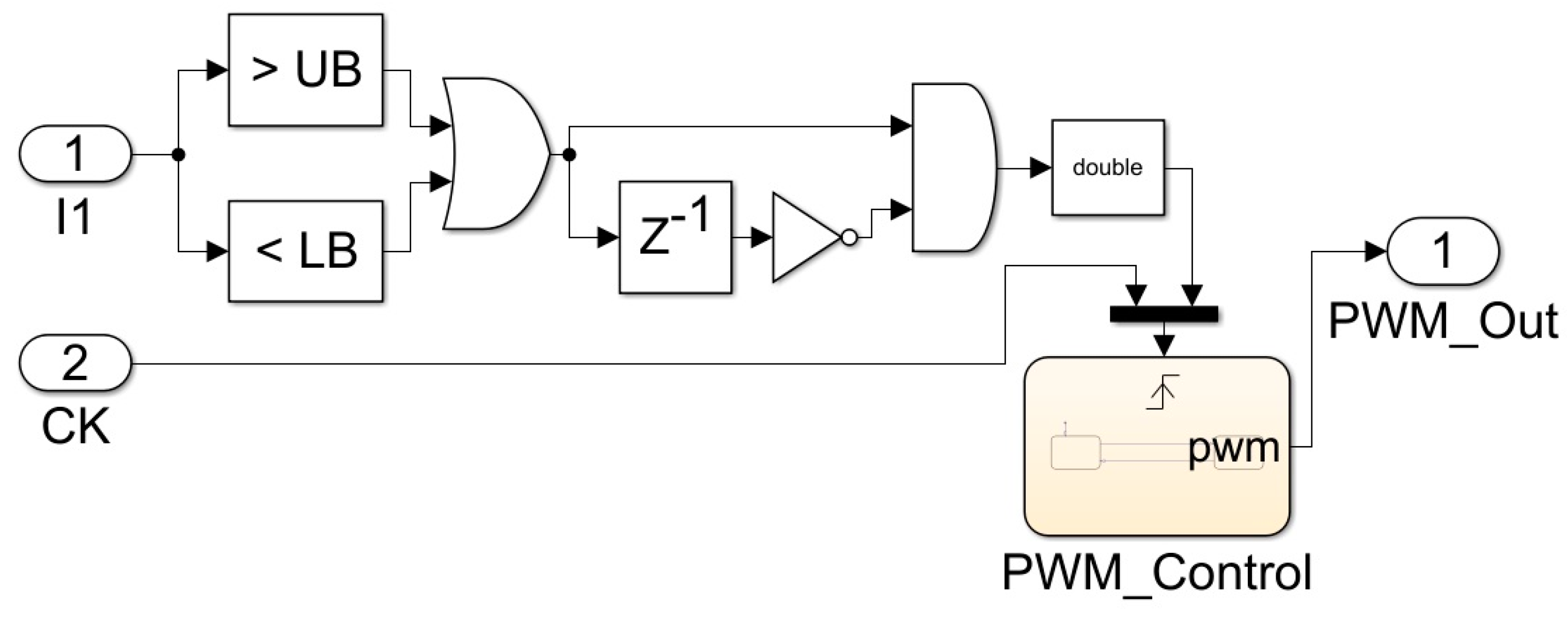
In Figure 5, the subsystem FPGA is represented. As shown in Figure 3, the measured output current has been used to control the PWM generation. For this purpose, two comparators have been instantiated on the FPGA subsystem.
When the output current oversteps the limits imposed by the comparators, the proposed control method sends a reset signal to synchronize the FSM that generates the PWM. The comparators must set up in order to limit the current in the Upper Bound (UB) and Lower Bound (LB). The lower bound is calculated as the minimum value of the load current (I0) divided by the number of the inverters (N). The upper bound is calculated as the lower bound plus the difference of the maximum and minimum load current divided by the number of inverters, as shown in (7) and (8).
The minimum current value (min(I0)) is the value of the initial simulation conditions: in this case it is 10 A. Meanwhile, the maximum current value (max(I0)) can be expressed as the value of the initial conditions plus the current excursion on the load.
These bounds are fixed to respect the normal behavior of the load current. In the setting of the comparators, their precision has been considered, estimating it as 10 mA. UB and LB have been rounded to the second decimal place to respect the precision of the comparators: the UB has been rounded down and the LB has been rounded up to consider a margin in respect to the maximum and minimum values. Due to the approximation, an increase in the PWM frequency can be seen because lower excursion of the current means higher oscillating frequency.
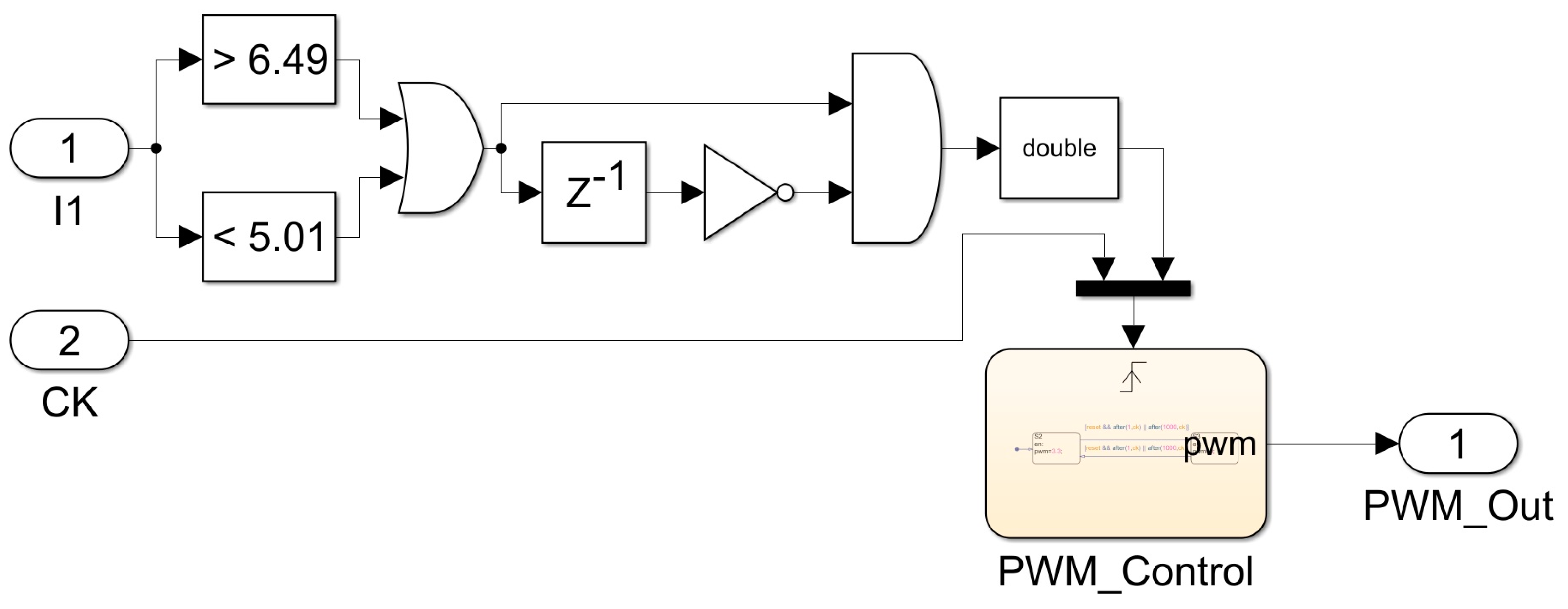
To better understand this control, a two parallel-connected inverters system has been simulated with a current operating point of 10 A on the load, which means an output current of 5 A for each inverter. In normal behavior, the load current starts from 10 A and increases until 13 A, and then returns to 10 A, forming a triangle waveform (because of the input square wave) respecting the PWM period. Specifically, when the PWM is in the high logical state, the current increases, and when the PWM is in the low logical state, the current decreases. This means that each inverter has an increase of 1.5 A from the initial operating point and the comparators should be set up at 5.01 A for the lower bound and at 6.49 A for the upper bound.
In Table 1, the configurations of the comparators for a number of parallel inverters ranging from 2 to 6 are reported.
In Figure 6, the proposed control method is shown, and the model-based design, with the value of UB and LB related to the case of a system with two parallel-connected inverters (5.01 A and 6.49 A, respectively), is described.
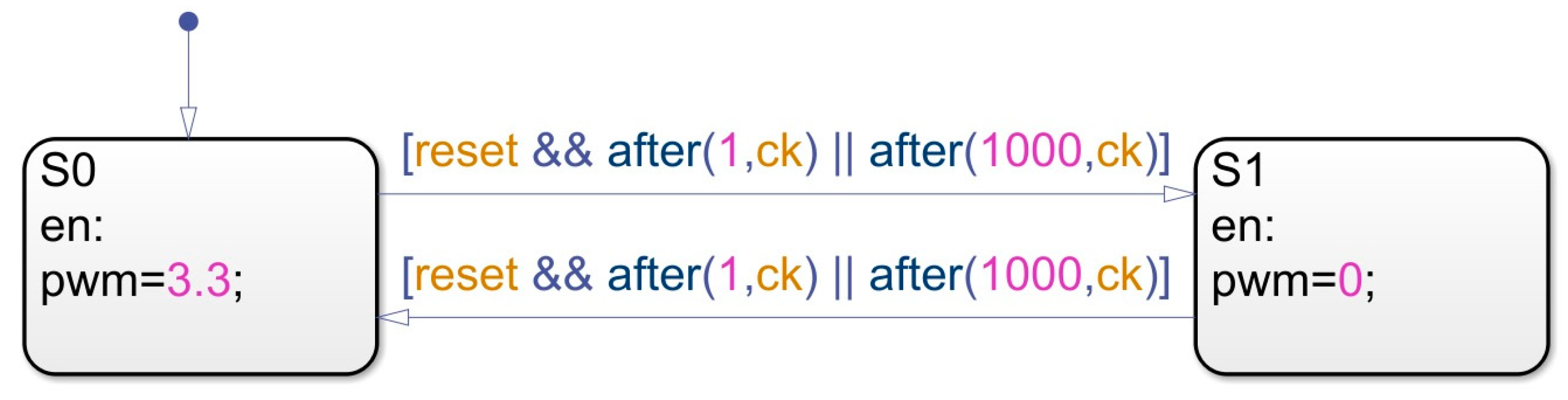
The FSM shown in Figure 7 has been used to generate the output PWM signal in the FPGA subsystem. In each inverter, the same FSM has been instanced. As shown in Figure 1, the designed inverter module is composed of the FPGA (low-power and logical part) which, through our algorithm, controls the power part (the BRIDGE). The algorithm is instanced in the FPGA, supplied with a voltage of 3.3 V, therefore, the two states correspond to the high logical level of 3.3 V in state S0 and to the low logical level 0 V in state S1. The transitions are governed by the external reset (bounds above mentioned) or by a fixed time, i.e., 10 μs (1000 clock rising edges), the PWM goes from the high logical level to the low logical level and vice versa, so the PWM with a frequency of 50 kHz is generated. Summarizing, a transition is executed if the FSM receives a reset signal or if 1000 clock cycles have passed.
The FSM default transition has been settled to the state S0, so the PWM starts always from the high logical level. The transitions with the reset signal are allowed only after one clock rising edge to prevent oscillations in the PWM change of state.
It is worth stressing that the proposed control method does not require an intercommunication line among the inverters; indeed, every inverter is equipped with an FPGA device with the described logic that controls only its own inverter.
3. Results and Discussion
To evaluate the control method, simulations of the model described in Simulink have been carried out. Firstly, the system with two inverters was tested; subsequently the algorithm has been revised to be used also on systems with a number N of inverters. In every simulation, circulating current, inverters output currents and PWM signals have been analyzed.
Table 2 shows the configuration for each inverter module used in the tests and, specifically, the clock frequency and the clock delay with respect the first inverter. As mentioned before, the frequency and the phase delay of the clock signals are not identical in every FPGA. The clock frequency of the first inverter has been taken as the reference, while the phase delay of the other inverters has been settled randomly with a delay between 1 ns and 5 ns.
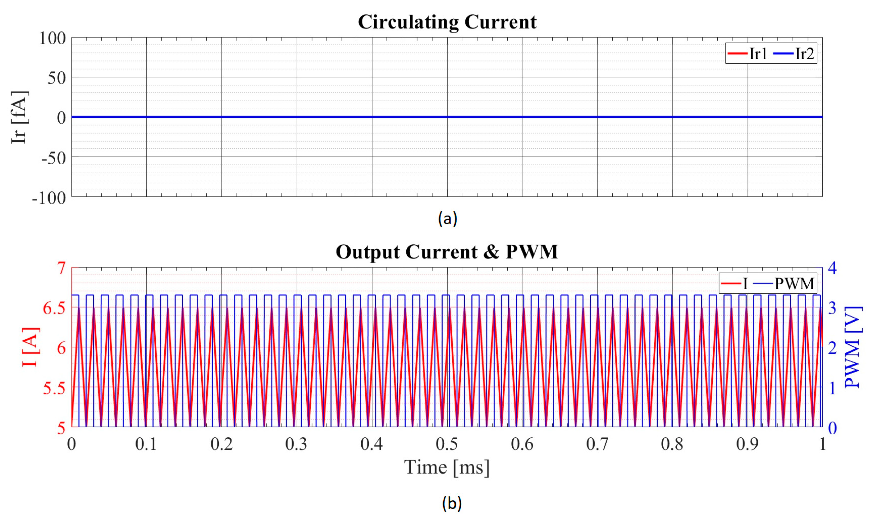
In Figure 8, the results of the simulations conducted with two parallel-connected inverters are reported: the trend over time of the circulating current, the PWM and the output current for each inverter are shown.
The graph reported in Figure 8a shows that the circulating current seen by the first inverter and the circulating current seen by the second inverter are equal to zero, confirming the quality of the proposed algorithm. Moreover, the PWM (drawn in blue) and the output current (drawn in red) are shown in Figure 8b. The PWM frequency is 50.668 kHz, a little higher with respect to the target frequency of 50 kHz due to the approximation and sensitivity of the comparators. The output currents are identical: they oscillate from 5.01 A to 6.49 A with a triangle waveform.
The configurations of the inverters used in the tests are the same shown in Table 2: the clock of the FPGA that controls the first inverter has been set up to 100 MHz with an initial current operating point of 5 A. The clock of the second has been set 0.1% higher than the first, precisely at 100.1 MHz with a phase delay of 5 ns. The initial current operating point has been set at 5 A for the second inverter; so on the load, the initial current operating point was at 10 A. The comparator settings are those reported in Table 1.
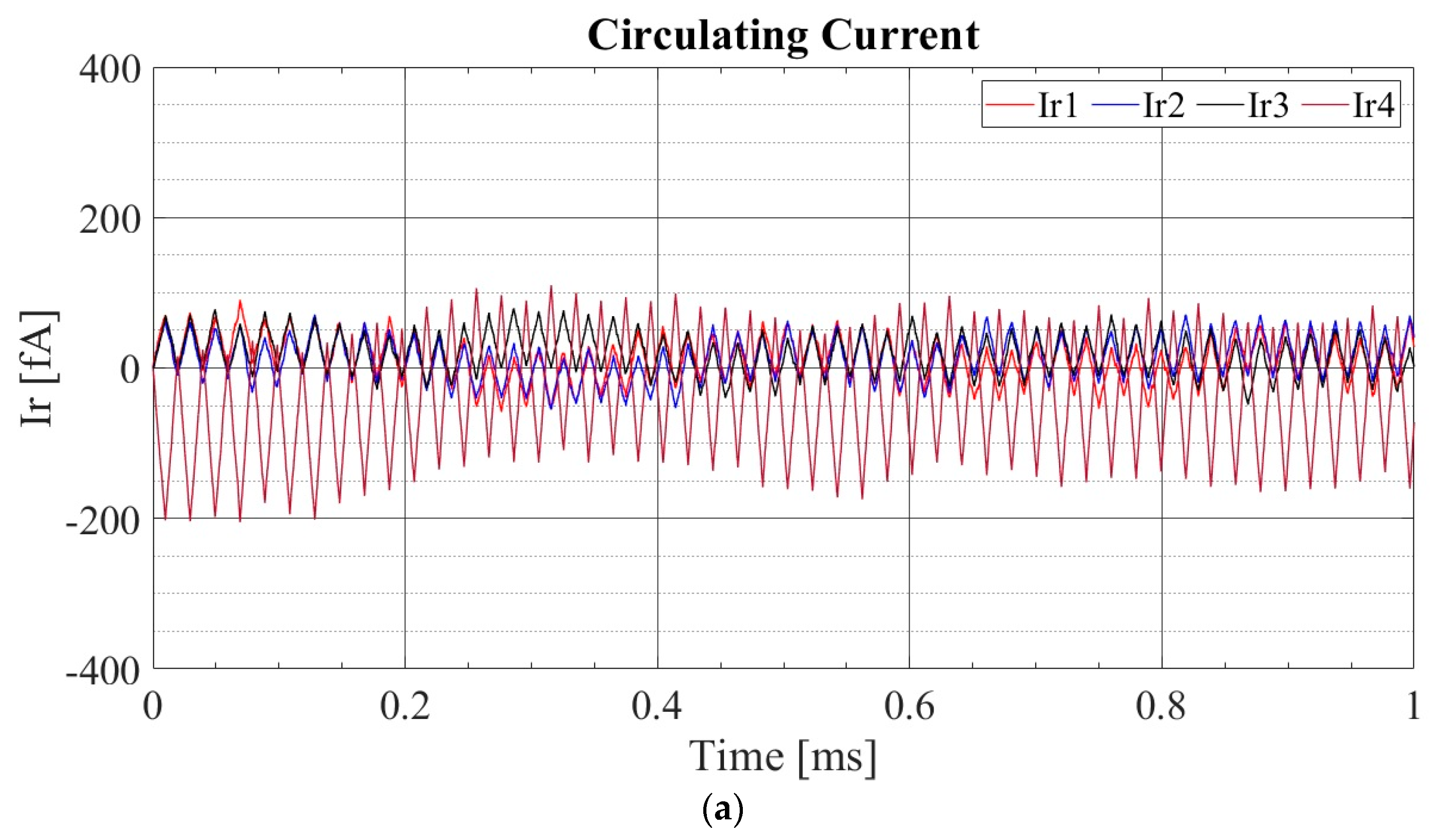
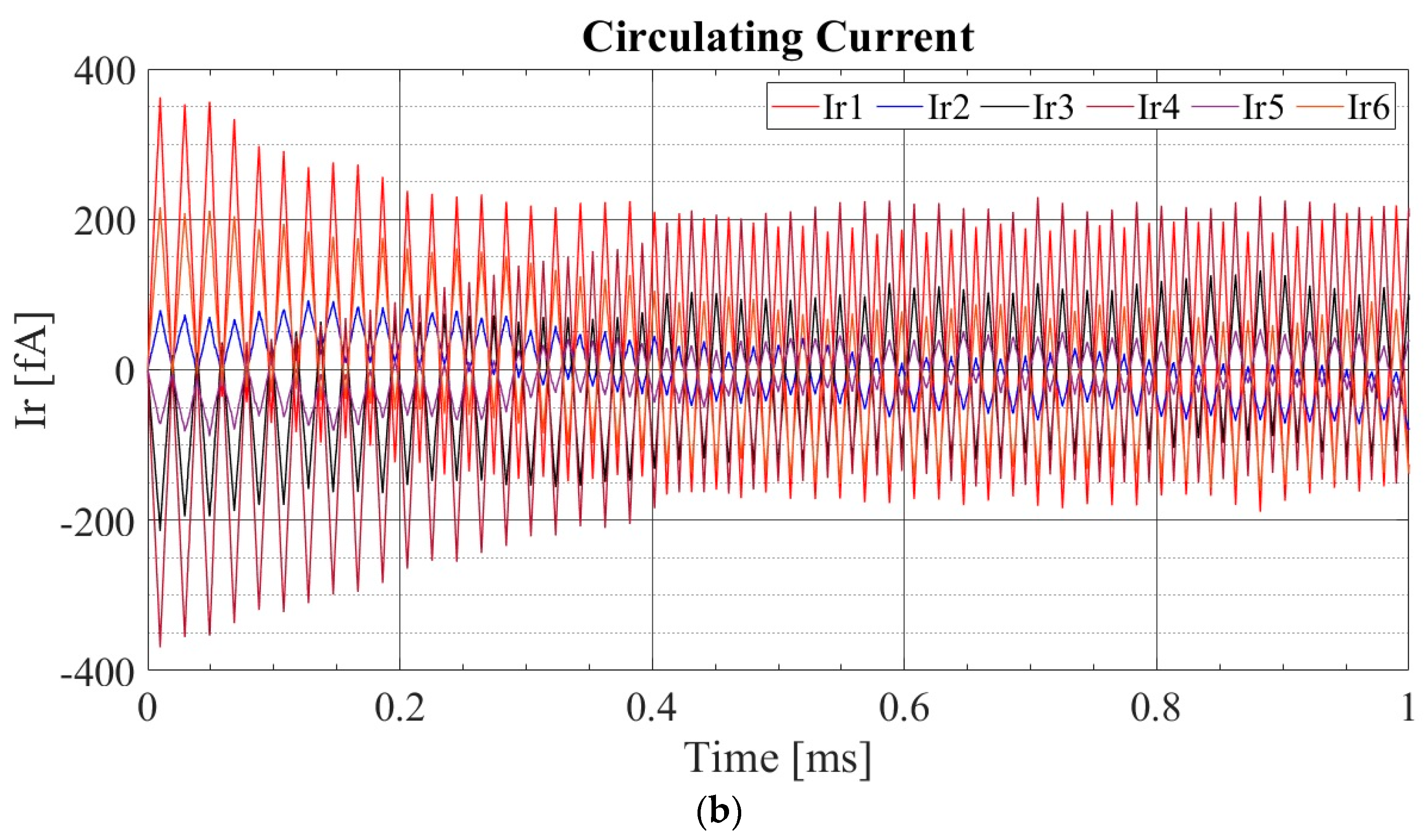
Subsequent tests are aimed at verifying whether the proposed method was applicable to a more general solution with N inverters. In Figure 9, circulating currents are reported with four and six inverters, respectively. In the case of the four inverters, Figure 9a, the initial condition of the load current has been set to 10 A, as described for the previous case. This current is equally distributed among the inverters (each inverter has an initial output current of 2.5 A). The amplitude of the circulating current is reduced to a few tens of femtoampere (fA) and the output current of each inverter is now reduced due to the greater number of inverters. The PWM frequency was considered 51.365 kHz, slightly greater than the setpoint (50 kHz). This error is caused by the precision of the comparators (estimated to 10 mA) as described before.
The waveforms represented in Figure 9b show the behavior of the circulating current in a system with six parallel-connected inverters. The circulating current remains in the range of the fA with a higher peak of 362 fA and a lower peak of −369 fA. The frequency of the PWM signal has been measured around 51.017 kHz for each simulation. As in the case of the two parallel inverters, the inverters’ parameters are those shown in Table 2 with comparators settings (UB and LB) shown in Table 1. Other configurations have been simulated and, in Table 3, results are reported. In particular, PWM frequency, the mean RMS value of the circulating current and the percent variation of the PWM frequency with respect to the target frequency for every system simulated, are shown.
A maximum frequency variation of 3.44% has been observed, obtained in the simulation with five parallel-connected inverters. Different results in frequency variations can be explained, considering that the comparators are configured by calculating the maximum and the minimum current values by dividing the total load current by the total number of parallel-connected inverters. In some cases, LB and UB (Equations (7) and (8)) must be approximated according to the values shown in Table 1 due to the precision of the comparators. These approximations can negatively affect the control accuracy by generating small differences in the PWM frequency.
Moreover, in Table 3, the residual circulating current after the application of the control is shown. The proposed control method is optimal in a two parallel-connected inverters system, as Figure 8 shows. The circulating current in that situation is equal to zero. Focusing on the other simulations, the circulating currents are not linearly dependent on the number of inverters connected to the system. There is no decrease in the circulating current due to a greater number of inverters, as shown in [26]. The reason is that the proposed control method reduces the circulating current by generating the PWM with the reset signals provided by the comparators. As explained in the previous paragraph, the approximations of Equations (7) and (8) can be strong, as in the four and six inverters case (higher circulating current), or weak, as in the case with three or five parallel-connected inverters (lower circulating current).
4. Conclusions
In this paper, a new control method for parallel-connected inverter systems has been presented and discussed.
The proposed method has been designed in a model-based fashion and simulated in a Simulink environment. The model is designed to be implemented on an FPGA, through a HDL coder—this technique allows one to reduce time to market and improve flexibility.
Each FPGA controls its inverter, a transmission line modelled as an impedance and the load, and the same circuit is instantiated on all system devices, enhancing modularity and scalability. Since a little phase delay or difference in the clock causes delays in the control response that generates the circulating current, a non-ideal clock for the FPGAs has been considered, and, in particular, a displacement from the nominal frequency of 0.1% has been simulated.
The simulations performed with a different number of inverters in parallel (up to six) demonstrate the ability of the control designed to reduce the circulating current and so reduce the risk of inverter damage. These results have been obtained without the necessity of any communication among the inverters that cooperate autonomously, each providing the same output current, unlike other authors that achieved the system control or the load sharing using communications lines or wireless communication among the inverters [34,35]. It has been demonstrated that the circulating current can be negligible in a system equipped with this control method, especially in a system with two parallel-connected inverters where the circulating current is equal to zero. Furthermore, when system control in a steady-state condition has been achieved with a modular and redundant structure, then, new inverters can be added without intervening on other parts of the system.
Author Contributions
Conceptualization, V.B., I.D.M.; methodology, V.B. and I.D.M.; validation, L.S., V.B.; formal analysis, L.S. and V.B.; investigation, L.S. and V.B.; data curation, L.S. and V.B.; writing—original draft preparation, L.S. and V.B. and I.D.M.; writing—review and editing, L.S. and V.B. and I.D.M.; visualization, L.S. and V.B. and I.D.M.; supervision, V.B. and I.D.M.; project administration, I.D.M.; funding acquisition, I.D.M. All authors have read and agreed to the published version of the manuscript.
Funding
This research received no external funding.
Institutional Review Board Statement
Not applicable.
Informed Consent Statement
Not applicable.
Data Availability Statement
Data available on request from the authors.
Conflicts of Interest
The authors declare no conflict of interest.
References
- Sharma, A.; Mathew, M.; Mitra, I.; Anwer, N. Approaches Leading to Different Definitions of Smart Grid: A Review. In Proceedings of the 2008 1st IEEE International Conference on Power Energy, Environment & Intelligent Control PEEIC2018, Uttar Pradesh, India, 13–14 April 2018; pp. 600–606. [Google Scholar] [CrossRef]
- IEA. Technology RoadmapSmart Grids; IEA: Paris, France, 2011; ISBN 9789813235342. Available online: https://www.iea.org/reports/technology-roadmap-smart-grids (accessed on 30 December 2020).
- Al-Badi, A.H.; Ahshan, R.; Hosseinzadeh, N.; Ghorbani, R.; Hossain, E. Survey of Smart Grid Concepts and Technological Demonstrations Worldwide Emphasizing on the Oman Perspective. Appl. Syst. Innov. 2020, 3, 5. [Google Scholar] [CrossRef] [Green Version]
- Watanabe, E.H.; de Araújo Lima, F.K.; da Silva Dias, R.F.; Aredes, M.; Barbosa, P.G.; Lima Barcelos, S.L.S.; Santos, G. Flexible AC Transmission Systems. In Power Electronics Handbook; Rashid, M.H., Ed.; Elsevier: Amsterdam, The Netherlands, 2018; pp. 885–909. [Google Scholar] [CrossRef]
- Atalik, T.; Deniz, M.; Koc, E.; Gercek, C.Ö.; Gultekin, B.; Ermis, M.; Cadirci, I. Multi-DSP and -FPGA-Based Fully Digital Control System for Cascaded Multilevel Converters Used in FACTS Applications. IEEE Trans. Ind. Inform. 2012, 8, 511–527. [Google Scholar] [CrossRef]
- Bhaskar, P.C.; Uplane, M.D. FPGA Based Digital FIR Multilevel Filtering for ECG Denoising. In Proceedings of the 2015 International Conference on Information Processing (ICIP), Pune, India, 16–19 December 2015; pp. 733–738. [Google Scholar] [CrossRef]
- Yuan, H.; Bi, M.; Chen, Z. FPGA Realization of Reactive Power Measurement System Based on FFT. In Proceedings of the 2012 7th IEEE Conference on Industrial Electronics and Applications (ICIEA), Singapore, 18–20 July 2012; pp. 2018–2022. [Google Scholar] [CrossRef]
- Bassoli, M.; Bianchi, V.; De Munari, I. A Model-Based Design Floating-Point Accumulator. Sensors 2020, 20, 1362. [Google Scholar] [CrossRef] [Green Version]
- Bianchi, V.; Bassoli, M.; De Munari, I. Comparison of FPGA and Microcontroller Implementations of an Innovative Method for Error Magnitude Evaluation in Reed–Solomon Codes. Electronics 2020, 9, 89. [Google Scholar] [CrossRef] [Green Version]
- Bianchi, V.; De Munari, I. A Modular Vedic Multiplier Architecture for Model-Based Design and Deployment on FPGA Platforms. Microprocess. Microsyst. 2020, 76, 103106. [Google Scholar] [CrossRef]
- Sivanandam, S.N.; Paulraj, M.P. Introduction to Artificial Neural Networks; Vikas Publishing: Uttar Pradesh, India, 2003; p. 236. ISBN 978-8125914259. [Google Scholar]
- Shawahna, A.; Sait, S.M.; El-Maleh, A. FPGA-Based Accelerators of Deep Learning Networks for Learning and Classification: A Review. IEEE Access 2019, 7, 7823–7859. [Google Scholar] [CrossRef]
- Sanaullah, A.; Yang, C.; Alexeev, Y.; Yoshii, K.; Herbordt, M.C. Real-Time Data Analysis for Medical Diagnosis Using FPGA-Accelerated Neural Networks. BMC Bioinform. 2018, 19, 19–31. [Google Scholar] [CrossRef] [Green Version]
- Chrysos, G.; Sotiriades, E.; Rousopoulos, C.; Dollas, A.; Papadopoulos, A.; Kirmitzoglou, I.; Promponas, V.; Theocharides, T.; Petihakis, G.; Lagnel, J.; et al. Opportunities from the Use of FPGAs as Platforms for Bioinformatics Algorithms. In Proceedings of the 2012 IEEE 12th International Conference on Bioinformatics & Bioengineering (BIBE), Larnaca, Cyprus, 11–13 November 2012; pp. 559–565. [Google Scholar] [CrossRef]
- Vetter, T.; Schulz, M. FPGA to Control Power Electronics. Power Electron. Eur. 2014, 6, 19–21. [Google Scholar]
- Sahu, N.; Londhe, N.D.; Kshirsagar, G.B. FPGA Applications in Inverter and Converter Circuits: A Review on Technology, Benefits and Challenges. In Proceedings of the 2017 International Conference on Innovations in Information, Embedded and Communication Systems (ICIIECS), Coimbatore, India, 17–18 March 2017; pp. 1–5. [Google Scholar] [CrossRef]
- Bianchi, V.; Savi, F.; De Munari, I.; Barater, D.; Buticchi, G.; Franceschini, G. Minimization of Network Induced Jitter Impact on FPGA-Based Control Systems for Power Electronics through Forward Error Correction. Electronics 2020, 9, 281. [Google Scholar] [CrossRef] [Green Version]
- Stellato, B.; Goulart, P.J. Real-Time FPGA Implementation of Direct MPC for Power Electronics. In Proceedings of the 2016 IEEE 55th Conference on Decision and Control (CDC), Las Vegas, NV, USA, 12–14 December 2016; pp. 1471–1476. [Google Scholar] [CrossRef]
- Borreggine, S.; Monopoli, V.G.; Rizzello, G.; Naso, D.; Cupertino, F.; Consoletti, R. A Review on Model Predictive Control and Its Applications in Power Electronics. In Proceedings of the 2019 AEIT International Conference of Electrical and Electronic Technologies for Automotive (AEIT AUTOMOTIVE), Torino, Italy, 2–4 July 2019; pp. 1–6. [Google Scholar] [CrossRef]
- Li, M.; Gao, W.; Xu, F.; Jiao, R. The Strategy of the Voltage Control in Smart Grid Based on Modern Control Method and FPGA. In Proceedings of the 2015 34th Chinese Control Conference (CCC), Hangzhou, China, 28–30 July 2015; pp. 8964–8968. [Google Scholar] [CrossRef]
- Guerrero, J.M.; Vásquez, J.C.; Matas, J.; Castilla, M.; García de Vicuna, L. Control Strategy for Flexible Microgrid Based on Parallel Line-Interactive UPS Systems. IEEE Trans. Ind. Electron. 2009, 56, 726–736. [Google Scholar] [CrossRef]
- Cai, H.; Zhao, R.; Yang, H. Study on Ideal Operation Status of Parallel Inverters. IEEE Trans. Power Electron. 2008, 23, 2964–2969. [Google Scholar] [CrossRef]
- Arbab-Zavar, B.; Palacios-Garcia, E.J.; Vasquez, J.C.; Guerrero, J.M. Smart Inverters for Microgrid Applications: A Review. Energies 2019, 12, 840. [Google Scholar] [CrossRef] [Green Version]
- Roslan, M.A.; Ahmad, M.S.; Isa, M.A.M.; Rahman, N.H.A. Circulating Current in Parallel Connected Inverter System. In Proceedings of the 2016 IEEE International Conference on Power and Energy (PECon), Melaka, Malaysia, 28–29 November 2016; pp. 172–177. [Google Scholar] [CrossRef]
- Saleem, M.; Ko, B.-S.; Kim, S.-H.; Kim, S.; Chowdhry, B.; Kim, R.-Y. Active Disturbance Rejection Control Scheme for Reducing Mutual Current and Harmonics in Multi-Parallel Grid-Connected Inverters. Energies 2019, 12, 4363. [Google Scholar] [CrossRef] [Green Version]
- Lu, M.; Wang, X.; Loh, P.C.; Blaabjerg, F. Resonance Interaction of Multiparallel Grid-Connected Inverters With LCL Filter. IEEE Trans. Power Electron. 2017, 32, 894–899. [Google Scholar] [CrossRef]
- Cavazzana, F.; Caldognetto, T.; Mattavelli, P.; Corradin, M.; Toigo, I. Analysis of Current Control Interaction of Multiple Parallel Grid-Connected Inverters. IEEE Trans. Sustain. Energy 2018, 9, 1740–1749. [Google Scholar] [CrossRef]
- Nalawade, R.P.; Joshi, P.M. Study of Circulating Current Phenomena in Multiple Parallel Inverters Operating in Microgrid. Int. J. Electr. Electron. Data Commun. 2015, 3, 9–14. [Google Scholar]
- De Brabandere, K.; Bolsens, B.; Van den Keybus, J.; Woyte, A.; Driesen, J.; Belmans, R. A Voltage and Frequency Droop Control Method for Parallel Inverters. IEEE Trans. Power Electron. 2007, 22, 1107–1115. [Google Scholar] [CrossRef]
- Kim, B.J.; Kum, H.J.; Park, J.M.; Won, C.Y. Analysis, Design and Implementation of Droop-Controlled Parallel-Inverters Using Dynamic Phasor Model and SOGI-FLL in Microgrid Applications. Energies 2018, 11, 1683. [Google Scholar] [CrossRef] [Green Version]
- Li, D.; Man Ho, C.N. Master-Slave Control of Parallel-Operated Interfacing Inverters Based on Wireless Digital Communication. In Proceedings of the 2018 IEEE Energy Conversion Congress and Exposition (ECCE), Portland, OR, USA, 23–27 September 2018; pp. 1466–1472. [Google Scholar] [CrossRef]
- Lazzarin, T.B.; Bauer, G.A.T.; Barbi, I. A Control Strategy for Parallel Operation of Single-Phase Voltage Source Inverters: Analysis, Design and Experimental Results. IEEE Trans. Ind. Electron. 2013, 60, 2194–2204. [Google Scholar] [CrossRef]
- Wei, B.; Guerrero, J.M.; Guo, X. Cross-Circulating Current Suppression Method for Parallel Three-Phase Two-Level Inverters. In Proceedings of the 2015 IEEE 5th International Conference on Consumer Electronics—Berlin (ICCE-Berlin), Berlin, Germany, 6–9 September 2015; pp. 423–427. [Google Scholar] [CrossRef] [Green Version]
- Guerrero, J.M.; García de Vicuña, L.; Matas, J.; Miret, J.; Castilla, M. A Wireless Load Sharing Controller to Improve Dynamic Performance of Parallel-Connected UPS Inverters. In Proceedings of the IEEE 34th Annual Conference on Power Electronics Specialist, 2003. PESC ‘03, Acapulco, Mexico, 15–19 June 2003; pp. 1408–1413. [Google Scholar] [CrossRef]
- Xiao, F.; Chen, W.; Liu, J.; Wang, H. Parallel Connected Three Phase Inverters Based on Modular Design and Distributed Control. In Proceedings of the 2014 International Power Electronics Conference (IPEC-Hiroshima 2014—ECCE ASIA), Hiroshima, Japan, 18–21 May 2014; pp. 72–77. [Google Scholar] [CrossRef]
- Niu, J.; Chen, R.; Zhang, Z.; Gui, H.; Wang, F.; Tolbert, L.M.; Blalock, B.J.; Costinett, D.J.; Choi, B.B. Design of a Single Controller for Multiple Paralleled Inverters. In Proceedings of the 2019 IEEE Applied Power Electronics Conference and Exposition (APEC), Anaheim, CA, USA, 17–21 March 2019; pp. 2524–2530. [Google Scholar] [CrossRef]
- Liao, Y.-H.; Chen, H.C. Simplified PWM With Switching Constraint Method to Prevent Circulating Currents for Paralleled Bidirectional AC/DC Converters in Grid-Tied System Using Graphic Analysis. IEEE Trans. Ind. Electron. 2015, 62, 4573–4586. [Google Scholar] [CrossRef]
- Soldati, A.; Undre, V.; Concari, C.; Alsayid, B.A.; Dradi, M.H. Parallel Operation of Voltage Source Converters without Filter Inductors: Control of the Circulating Current. In Proceedings of the 2020 2nd IEEE International Conference on Industrial Electronics for Sustainable Energy Systems (IESES), Cagliari, Italy, 1–3 September 2020; pp. 125–130. [Google Scholar] [CrossRef]
- Silicon Labs Ultra Series TM Crystal Oscillator Si541 Data Sheet; Silicon Labs: Austin, TX, USA, 2018.
- Silicon Labs Si 530/531 Crystal Oscillator Data Sheet; Silicon Labs: Austin, TX, USA, 2018.
Figure 1.
Schematic of a general parallel-connected inverter system.

Figure 2.
Schematic of a two parallel-connected inverters system.

Figure 3.
Simulink model of the system with two inverters.

Figure 4.
Simulink model of the subsystem “BRIDGE”.

Figure 5.
Simulink model of the subsystem FPGA.

Figure 6.
Subsystem Field Programmable Gate Array (FPGA) in a system with two inverters.

Figure 7.
FSM generating the output PWM signal in the FPGA subsystem.

Figure 8.
Simulations with two parallel-connected inverters: (a) circulating current seen by the two inverters; the zero value obtained shows the validity of the algorithm; (b) PWM waveform and output current.
Figure 8.
Simulations with two parallel-connected inverters: (a) circulating current seen by the two inverters; the zero value obtained shows the validity of the algorithm; (b) PWM waveform and output current.

Figure 9.
Simulated circulating current: (a) system with four parallel-connected inverters; (b) system with six parallel-connected inverters.
Figure 9.
Simulated circulating current: (a) system with four parallel-connected inverters; (b) system with six parallel-connected inverters.


Table 1.
Comparator configurations.
| Number of Parallel Inverters | |||||
|---|---|---|---|---|---|
| 2 | 3 | 4 | 5 | 6 | |
| LB [A] | 5.01 | 3.34 | 2.51 | 2.01 | 1.67 |
| UB [A] | 6.49 | 4.33 | 3.24 | 2.59 | 2.16 |
Table 2.
Inverters configurations.
| fclk [MHz] | δ [ns] | |
|---|---|---|
| Inverter 1 | 100 | 0 |
| Inverter 2 | 100.1 | 5 |
| Inverter 3 | 100.1 | 3 |
| Inverter 4 | 100.1 | 2 |
| Inverter 5 | 100.1 | 1 |
| Inverter 6 | 100.1 | 1 |
Note: δ represents the clock delay with respect the first inverter.
Table 3.
Inverters’ configurations.
| Number of Inverters in the System | fPWM [kHz] | IrRMS [fA] | Frequency Variation [%] |
|---|---|---|---|
| 2 | 50.668 | 0 | 1.38 |
| 3 | 50.500 | 15.910 | 1.00 |
| 4 | 51.365 | 46.502 | 2.73 |
| 5 | 51.720 | 16.956 | 3.44 |
| 6 | 51.017 | 78.200 | 2.03 |
Publisher’s Note: MDPI stays neutral with regard to jurisdictional claims in published maps and institutional affiliations. |
© 2021 by the authors. Licensee MDPI, Basel, Switzerland. This article is an open access article distributed under the terms and conditions of the Creative Commons Attribution (CC BY) license (http://creativecommons.org/licenses/by/4.0/).
Share and Cite
MDPI and ACS Style
Saccenti, L.; Bianchi, V.; De Munari, I. Study of a Synchronization System for Distributed Inverters Conceived for FPGA Devices. Appl. Syst. Innov. 2021, 4, 5. https://0-doi-org.brum.beds.ac.uk/10.3390/asi4010005
AMA Style
Saccenti L, Bianchi V, De Munari I. Study of a Synchronization System for Distributed Inverters Conceived for FPGA Devices. Applied System Innovation. 2021; 4(1):5. https://0-doi-org.brum.beds.ac.uk/10.3390/asi4010005
Chicago/Turabian StyleSaccenti, Leonardo, Valentina Bianchi, and Ilaria De Munari. 2021. "Study of a Synchronization System for Distributed Inverters Conceived for FPGA Devices" Applied System Innovation 4, no. 1: 5. https://0-doi-org.brum.beds.ac.uk/10.3390/asi4010005