10 kV SiC MOSFET Evaluation for Dielectric Barrier Discharge Transformerless Power Supply


Laplace Laboratory, Université de Toulouse, CNRS, INPT, UPS, 2 rue Charles Camichel, F-31071 Toulouse, France
*
Author to whom correspondence should be addressed.
Plasma 2020, 3(3), 103-116; https://0-doi-org.brum.beds.ac.uk/10.3390/plasma3030009
Submission received: 20 March 2020
/
Revised: 14 August 2020
/
Accepted: 16 August 2020
/
Published: 18 August 2020
Abstract
:At low pressure, cold plasmas are used for a wide range of applications such as coating, flow control, or microelectronics. Currently, this industry requires expensive vacuum systems which consume energy and time, and therefore it is very appealing to develop similar processes at atmospheric pressure. Under this condition, dielectric barrier discharge (DBD) is one of the best ways to obtain a cold plasma. The dielectric barriers naturally limit the current, and then the plasma temperature. Unfortunately, at atmospheric pressure the discharge ignition between the electrodes requires high voltage, which is generally obtained through a step-up transformer. The parasitic elements of this device exclude a smart control for the discharge. In order to overcome this default, we analyze the performance of a transformerless power supply developed with a recently released single-chip high-voltage semiconductor. The circuit uses only two high-voltage switches synthesized by means of the 10 kV SiC MOSFET (Metal Oxide Semiconductor Field Effect Transistor). The design and implementation of the electric converter are presented and validated with experiments carried out on UV excimer DBD lamps. Then, the performances of the 10 kV SiC switches are analyzed and the relevance of this device for DBD applications is discussed.
1. Introduction
From an electrical point of view, cold plasmas are complex loads to control: for ignition, high voltages are required, and once established at atmospheric pressure, the plasma can easily go into an arc regime (thermal plasma). In dielectric barrier discharge (DBD) [1] setups, at least one dielectric is placed between the two electrodes that supply the power to the gas. When current flows through the plasma, it also charges the dielectric covering. The dielectric voltages increase, and thus the gas voltage decreases. Through this limiting mechanism, the capacitive character of the dielectric barriers limits the current, and therefore prevents transition into the arc regime. This property makes the DBD particularly appealing for various applications that require low temperatures plasmas such as UV excimer lamps [2], thin film deposition, surface treatment [3], flows control [4] and disinfection [5]. Our developments are geared toward a DBD UV lamp, an especially easy to use DBD reactor, for which performance is easy to measure with a simple photodetector; nevertheless, the approach proposed, in this paper, is not restricted to this specific DBD application.
The capacitive character of the DBDs requires supplying these setups using an alternative source. Early DBD experiments used sinusoidal voltage sources in frequencies ranging from tens of hertz to tens of megahertz [1], and later pulsed voltage sources [2] and voltage-mode resonant converters [5,6]. All these solutions suffer from a reduced ability to predict and control the injected power. Considering the DBD electrical lamp model (see Section 2), it has been established that DBD electrical power is better controlled by its current than its voltage [7,8]. Additionally, the UV emission of the bulbs is directly proportional to the current flowing through the gas.
Furthermore, to ignite the discharge at atmospheric pressure, the applied voltage usually reaches several kilovolts. This high alternating voltage is traditionally obtained via amplification using a step-up transformer. Unfortunately, the parasitic elements of the transformer (leakage inductance, inter-turn and inter-winding parasitic capacitance) limit the power transfer:
Parasitic capacitance has very low values (generally some 10 pF), commonly, in the same order of magnitude as those of the DBD. Being parallel to the DBD, it diverts a significant part of the transferred current [9]. This capacitance avoids controlling the current injected in the discharge. Moreover, it slows down the voltage rise and delays the ignition of the discharge. For example, at 10 kHz, discharges occur each 50 µs (twice in a period). In this case, the plasma ignition is delayed by 10 µs, which is 20% of the operating period [10]. Therefore, the main problem of the parasitic capacitance concerns the functioning of the discharge, indeed, during this uncontrolled OFF time, the excited species created by the previous discharge disappear. In some processes, this reduction of the memory effect changes the behavior of the discharge [3].
Because of the high-voltage transformer, the transferred power and the discharge behavior are far from being optimally controlled. This incited us to investigate supply structures where the transformer could be eliminated. In this domain, many investigations have been conducted over the decades. Basically, resonant circuit properties were able to boost the voltage. Recent works have proposed resonant voltage sources [11,12], in which a low-voltage inverter, using common semiconductor switches, was connected to an L-C resonant circuit. Another solution was to supply the DBD directly with a high-voltage inverter. This circuit could use high-voltage gas switches [13] or semiconductor switches. This last solution is currently used in many applications such as plasma synthetic jet actuators [14], DBD plasma jet for medical application [15,16], or coating application [17]. Nowadays, researchers commonly use commercial pulsers (DEI or BEHLKE) made with high-voltage switch assemblies [18]. In these devices, numerous semiconductors are connected in series in order to sustain the high voltage. Some devices also arrange component strings in parallel, in order to increase the maximum current. In all cases, considering controlled switches, all the transistors must be switched rigorously synchronously and the voltage balance between each transistor must be controlled accurately. Until very recently, the series connection was the only solution to sustain high voltage, because a single transistor was unable to hold a voltage higher than 2 kV. Recently, large gap semiconductor research has resulting in the design of SiC DMOSFETs which are able to sustain 10 kV. Their rated voltage level makes them suitable for a wide range of DBD applications. In this paper, we present our evaluation of this technology in the context of a transformerless DBD power supply. To our knowledge, in this scope, only theoretical developments [19] have been proposed to date, because high-voltage semiconductors have only been available for a few years. The semiconductor devices are 10kV SiC power DMOSFETs, designed by the CREE Company, which are not yet on the market but are similar to those used in [20]. On this basis, an innovative transformerless pulsed-current source topology is proposed in Section 2, where the switches are directly connected to the DBD high voltage. This power supply directly controls the energy injected into the discharge during each period; the theoretical approach of this solution was the subject of a previous (2017) publication [21]. In the current paper, we propose a complete sizing of the power supply and we justify the choice of each component, notably the 10kV SiC MOSFETs [21] and diodes, as presented in Section 3. The experimental setup, performance analysis, notably through a power balance, and results are discussed in Section 3 and Section 4.
2. Materials and Methods
In this section, we present the proposed transformerless topology: its operating principle, the sizing equations, derived from the analytical equations of the electrical constraints, the selection of high voltage semiconductors and the test bench for experimental investigations.
2.1. DBD Load Properties and Modeling
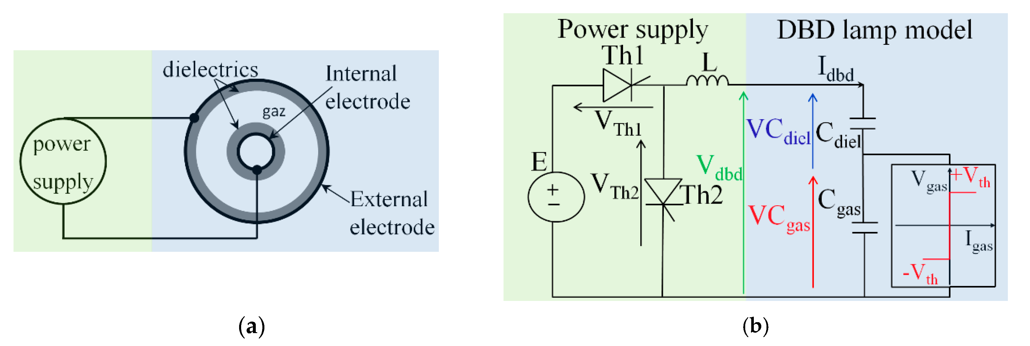
In a power-supply design approach, modeling of the DBD load is developed below [22,23,24]. The DBD used for the experiments is a cylindrical configuration excimer UV lamp [2], with two coaxial tubes of quartz (see Figure 1a) containing a gas mixture (Xe-Cl) and metal electrodes placed (metallic mesh) on the outer walls.
As long as the discharge is not initiated, the voltage is applied to the dielectric and the gas. The capacitance of the two dielectrics in series is defined by Cdiel and the capacitance of the gas by Cgas. Generally, Cgas << Cdiel. In the OFF state, the DBD is equivalent to the series Ceq capacitance, approximately equal to Cgas. When the discharge is in the ON state, we consider that the gas voltage does not change and remains at the breakdown level, ±Vth (the sign depends on the direction of the current). This assumption is valid when the discharge is a Townsend or glow discharge. It concerns a macroscopic point of view and does not take local phenomena into account, but it is largely sufficient to consider the electrical non-linearity of the plasma. As shown in Figure 1b, the discharge is modeled by a (Vgas, Igas) dipole, that reflects the breakdown mechanism; this dipole is parallel to the gas capacitance Cgas.
2.2. Operating Principle of the Transformerless Topology
Here, an analytical study of the converter is conducted, in order to present its operating principle. Taking the electrical characteristics of the gas into consideration, to control the power injected into the gas, the Idbd current flowing through the DBD must be controlled. Because of the capacitive behavior of the device, this current must have an average value of zero. An inductor is placed in series with the DBD and the direction of the current is controlled with the states of the switches. The inductance forms a resonant tank with the DBD and directly controls the current injected into the discharge. On the basis of the switches’ electrical constraints (voltage and current waveforms) described in the following part, the static and dynamic characteristics of both semiconductors can be shown to be those of thyristors. There are no thyristors on the market in the range of the target frequencies (tens of kHz), therefore, this function is synthesized by combining a MOSFET and a diode in series (see Figure 2b) [25].
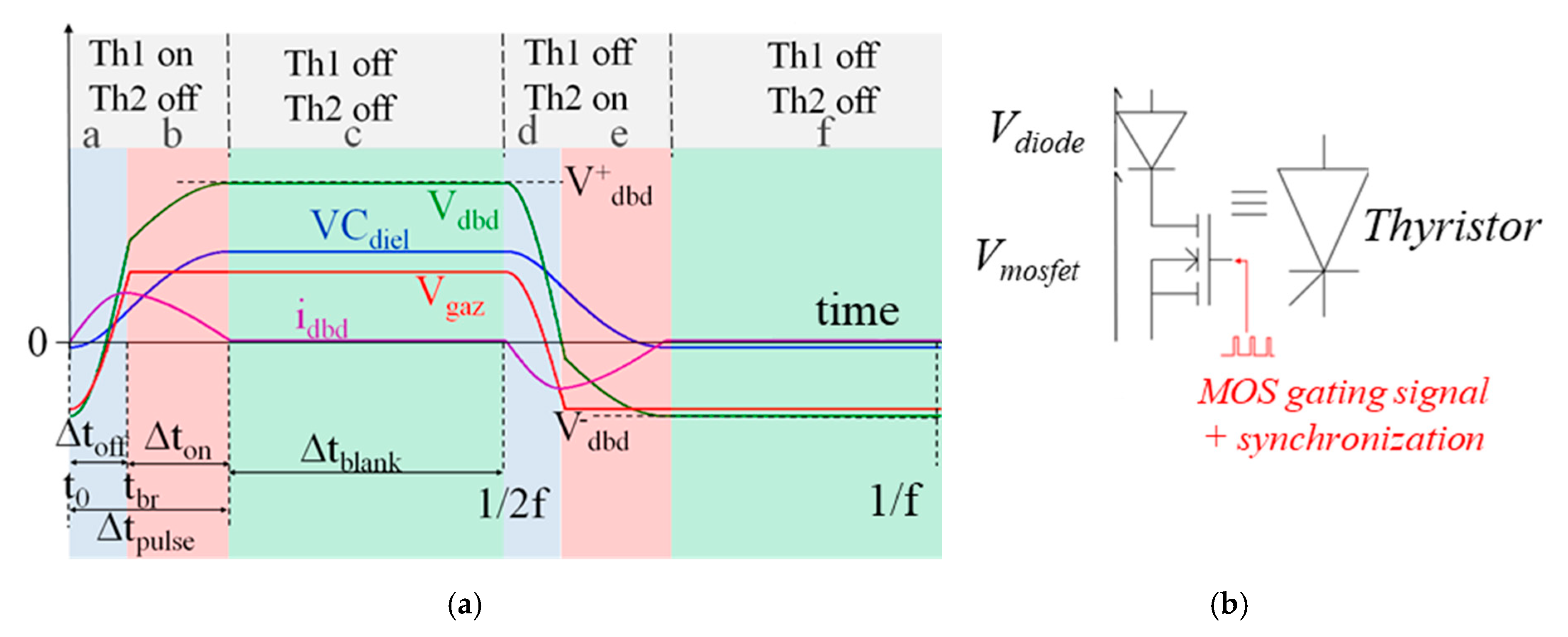
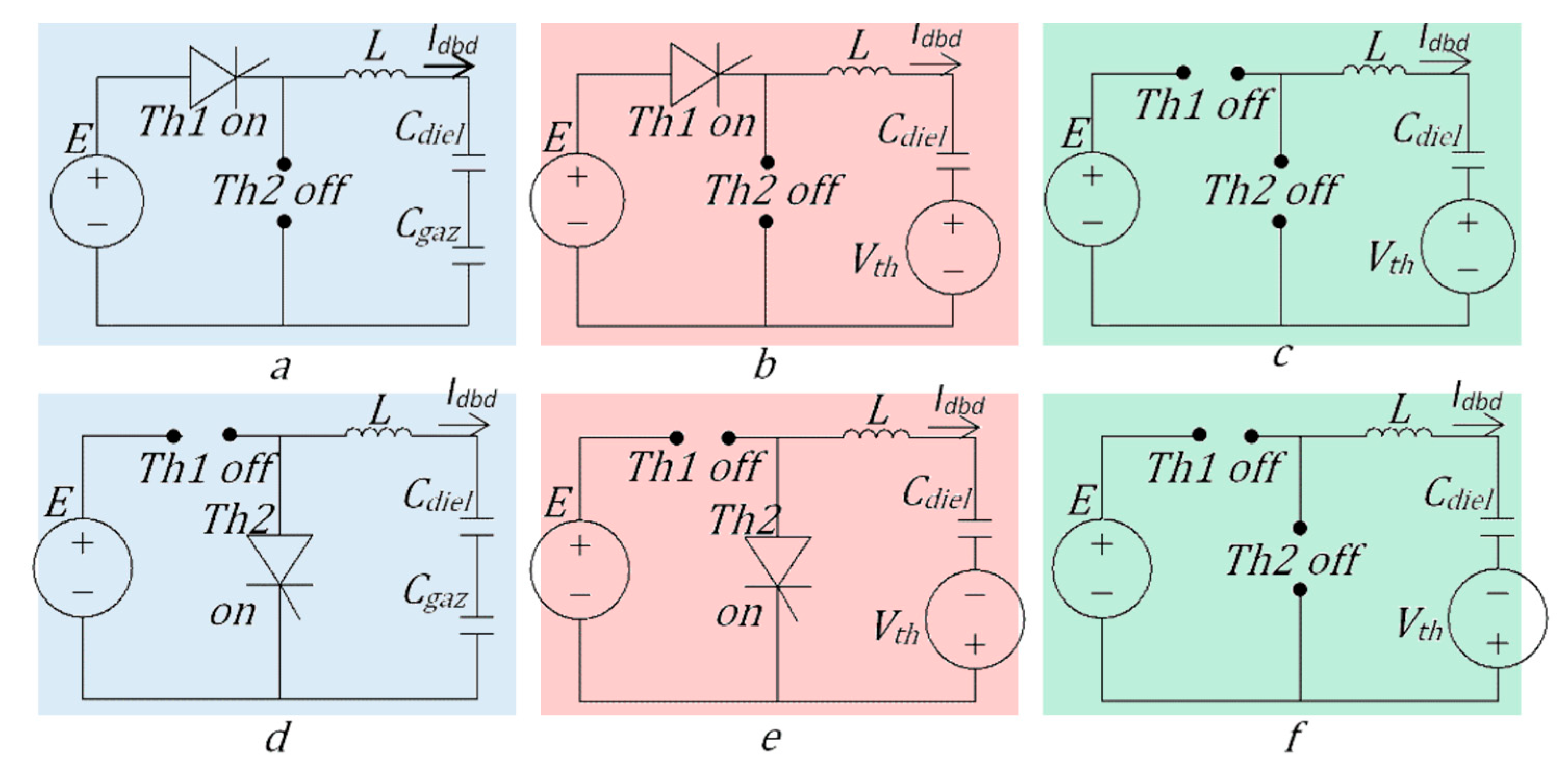
The steady-state operation of the converter presented in Figure 2a can be divided into six stages, based on, on the one hand, the state of the switches, and on the other hand, the state of the gas. The equivalent circuit of each stage is shown in Figure 3.
By initiating Th1 (Th2 remaining blocked), a resonant loop is activated; the voltage and current quantities of the discharge are governed by the resonant circuit, LCgas, Figure 3a, during a time interval, ∆toff. As the DBD is initially negatively charged, Vdbd and Vgas increase until the discharge is ignited with a positive current (when Vgas reaches Vth the breakdown level). From this time, during time interval ∆ton, the Vgas voltage remains constant at +Vth, while the Vdbd voltage and the Idbd current are governed by the LCdiel circuit, Figure 3b, until the Idbd current drops to zero. This event causes Th1’s diode to turn OFF. The discharge extinguishes (Sequence (c)) and its voltage does not change until Th2 is initiated.
Subsequently, Th2 is initiated (Th1 remains blocked). The DC power source is not electrically connected to the DBD, but the electrical charges stored on the dielectric are used to ignite a new discharge with a negative current. The DBD and the inductor are short circuited and their waveforms are governed by the same resonant circuit, LCgas when the discharge is OFF, Figure 3d, and LCdiel when it is ON, Figure 3e. The waveforms of Vgas and Idbd are symmetrical with respect to those obtained in the first half period. Because of the half bridge configuration, Vdbd voltage is not symmetrical.
2.3. Semiconductor Selection: Analytic Study of the Operation and Sizing Equations
The aim of this section is to find out the values of voltage and current stresses of MOSFETs and diodes used for Th1 and Th2. As can be seen on Figure 1b:
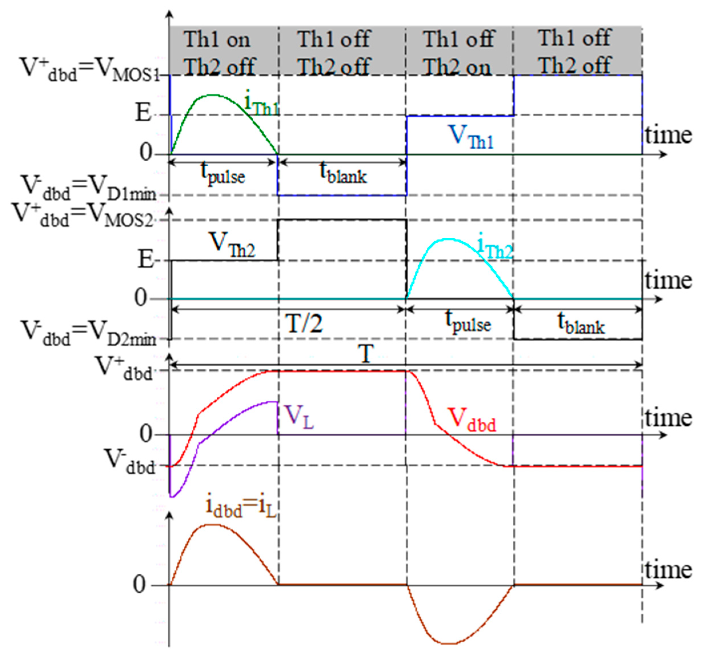
Figure 4 presents the main waveforms related to the electrical stresses in the semiconductors; these are obtained using a circuit simulator [26]. When Th1 is closed, the voltage across its terminals is zero; the voltage across Th2 is equal to the power supply voltage E. The inductance current is in the form of a pulse and the DBD voltage increases. Immediately after the zero crossing of the current in the inductor, several events happen. The thyristor Th1 is blocked and the DBD voltage no longer changes, remaining at its positive value V+dbd. Then, the inductor voltage VL is zero because no current flows through it, hence, the DBD voltage is seen by Th2. According to the Equation (1), Th1 supports (E − V+dbd); this negative voltage is denoted V−dbd and is held by the diode D1 of Th1, until the end of the half period.
When Th2 is closed (Th1 remains opened), the DBD is no longer connected to the voltage source. In this case, the E source imposes its voltage to Th1, while there is current flowing through Th2. Now, the DBD voltage decreases. Following the cancelation of the current in the inductor, the blocking voltage of the thyristor Th2 and the DBD voltage remain at V−dbd. The thyristor Th1, then, supports the voltage (E − V−dbd). This positive voltage is V+dbd and is supported by the MOSFET (MOS1) of Th1. To resume, each MOSFET supports a maximum voltage equal to V+dbd and each diode a negative voltage equal to V−dbd. The current through the semiconductors is equal to the current of the DBD. In our case, it is not a limiting parameter.
The converter’s operation is studied from the model shown in Figure 1b, using the state plan analysis [27] method, considering steady state conditions. This analysis enables the transient current-voltage characteristic of a resonant circuit to be plotted. Therefore, joint evolutions of the normalized values of the voltage and the DBD’s current are studied. Durations and peak voltages and currents, for operating stages (a) and (b) presented in the previous section, are calculated using trigonometric analysis; using the symmetry of the waveforms, this information allows one to describe the whole period. Calculations are detailed in [21] and results are summarized in Table 1 below:
We can also deduce the maximum current:
The duration of the current pulse injected into the DBD is denoted ∆tpulse. It defines the minimal duration of the half switching period of the MOSFETs as:
∆tpulse mainly depends on the inductance, L, and the capacitance of the DBD. Therefore, knowing the DBD’s capacitance enables the inductance, L, to be sized with respect to Equation (3), using the formula given in Table 1b. A second advantage of this topology is that the magnitude of the discharge current pulse is also controlled by the value of the inductance. Moreover, the MOSFET’s switching frequency can directly control the power transferred to the discharge (Equation (4)).
2.4. High-Voltage Switch Opportunities
The proposed topology offers the opportunity to implement zero current switching (ZCS) conditions of the MOSFETs at turn OFF, as well as at turn ON. When sizing the inductance L, the pulse duration ∆tpulse is chosen, and therefore defines the moment when the diode spontaneously turns OFF. Then, the turn-OFF control order of the MOSFET is sent 1 µs after ∆tpulse (and always before T/2). With this condition, we are sure that the MOSFET is turned off when there is zero current (ZCS operation). This minimizes the switching losses and requires the discontinuous mode translated by Equation (3).
As seen in previous lines, MOSFETs have to withstand V+dbd, while the diodes must hold V−dbd. Preliminary SiC power DMOSFETs from company CREE with a 10 kV maximum drain to source voltage are used [28]. Series connected low-voltage MOSFETs [29] have been considered as well, but this solution, which is not presented in this paper, requires static and dynamic voltages balancing. For the diodes, preliminary SiC diodes from CREE, holding up to 10 kV, are used. To limit the parasitic effects that alter the operation described in the previous section, diodes with low parasitic capacitance are favored.
High-voltage switch control, with high-voltage transistors, and especially for Th1 MOSFET in our topology, is very important to isolate the control boards from the power. The DE0 [30] FPGA board which controls the supply’s operation is connected to the driver cards via optical fibers.
2.5. Experimental Setup and Measurement
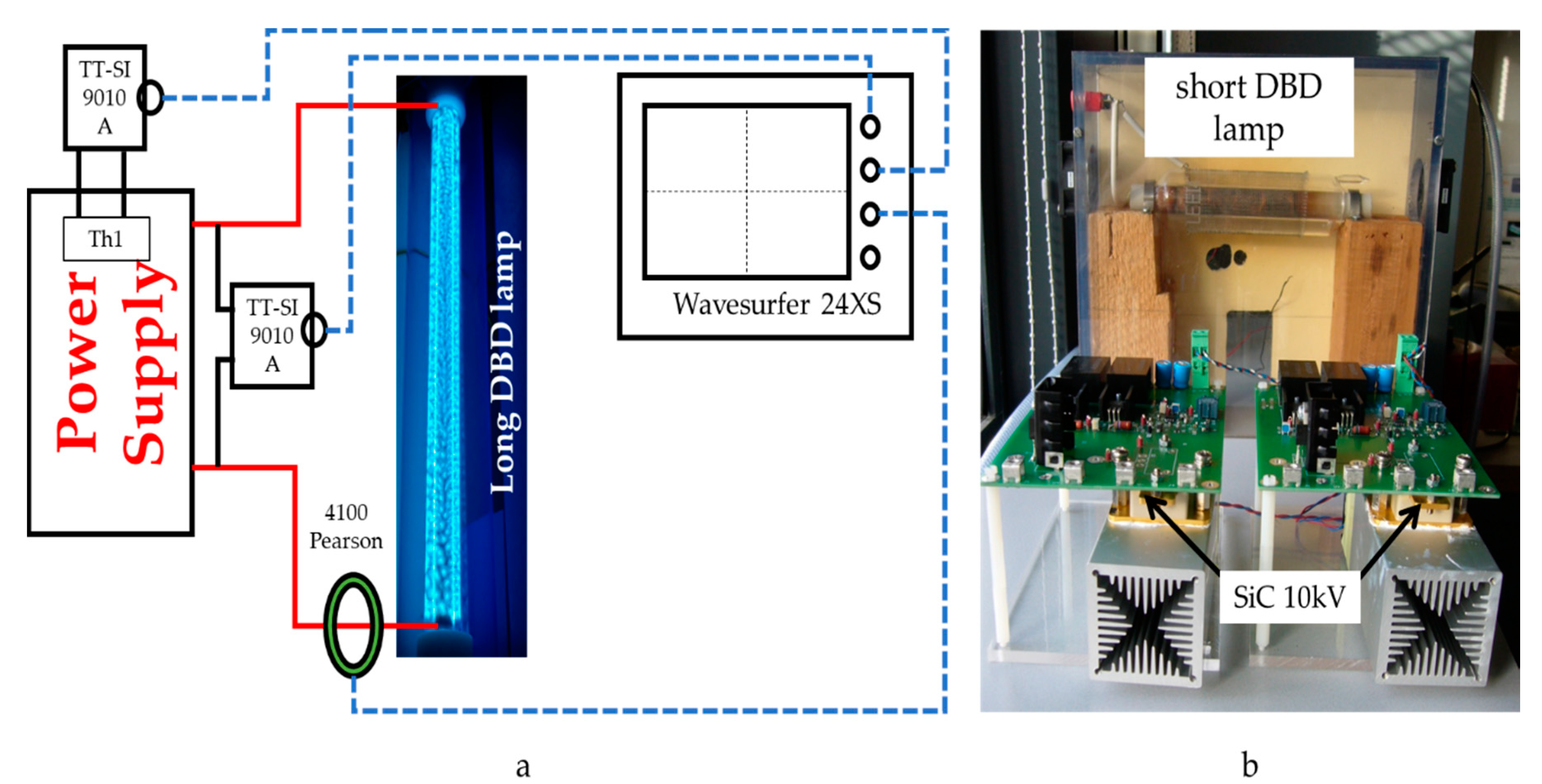
Here, the experimental validation of the converter is achieved by using a DBD lamp with an outer diameter of 45 mm, an inner diameter of 20 mm, and length of 60 cm tubes have a 2 mm thickness. This lamp is filled with an Xe-Cl mixture and the gas breakdown voltage is Vth = 1310 V. This breakdown voltage is not the voltage applied across the terminals of the bulb, it is only the voltage across the gas gap. The applied voltage sums this gas voltage and the dielectrics voltages. To calculate Vth, we use measurements of the electric signals applied to the DBD (VDBD and IDBD) and the electrical model of the DBD presented in Figure 1. The electrical parameters of the bulb are summarized in Table 2. Measurements and calculations of these data are taken as per the approach set out in [23,24]. In the Discussion Section 4 we compare the performance of the whole system, using this long lamp and a short one (with same tubes diameters), as presented in Figure 5b.
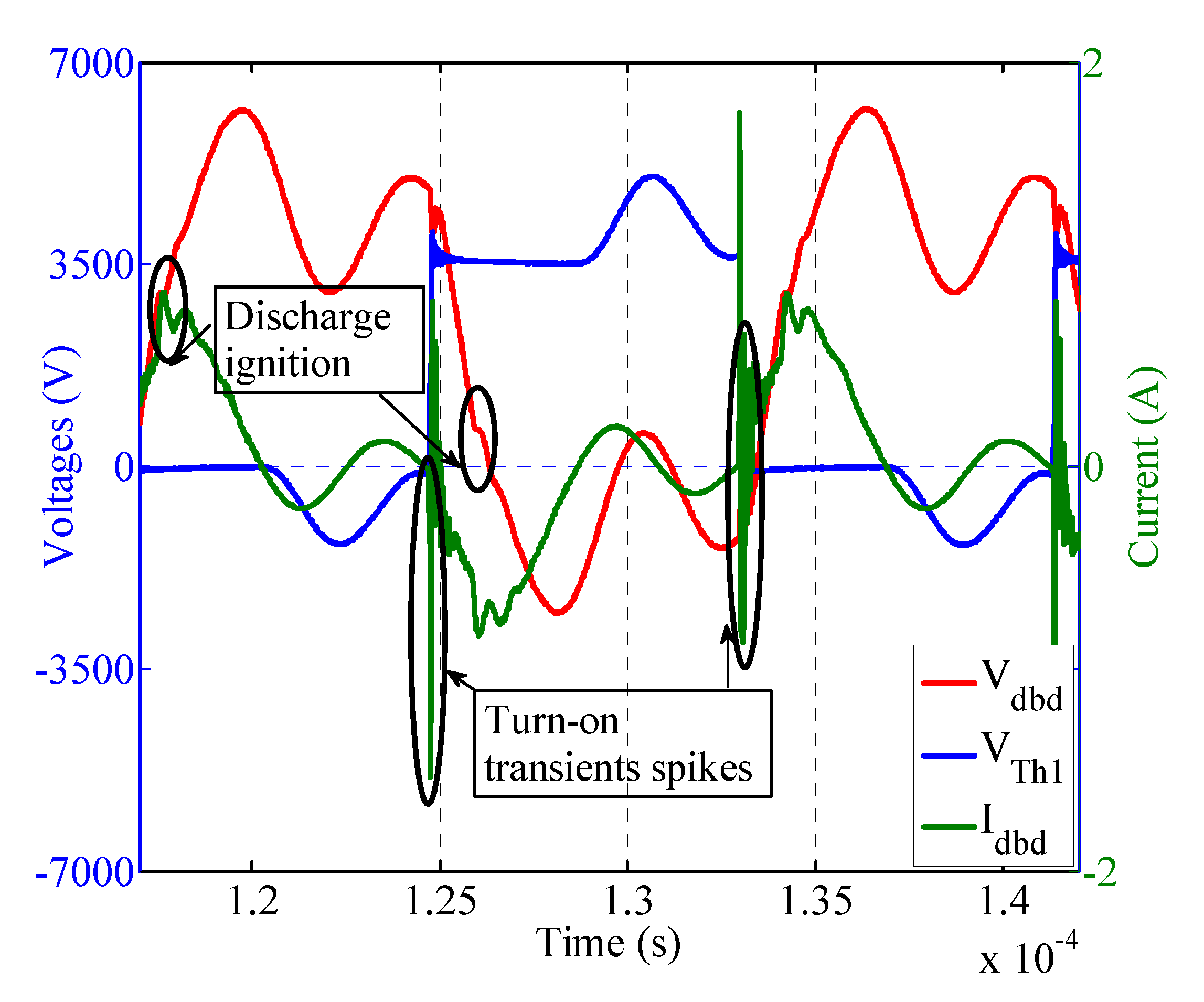
As shown in Figure 5, voltages are measured using high-voltage differential probes, TESTEC TT-SI 9010A (Frankfurt, Germany), with a bandwidth of 70 MHz (parasitic capacitance: approximately 12 pF). The discharge current is measured using a 4100 Pearson (Palo Alto, CA, USA) probe with a bandwidth of 20 MHz. Electrical waveforms are observed and recorded using a LECROY Wavesurfer 24XS oscilloscope (Thousand Oaks, CA, USA). The E voltage source is a 10 kV DC power supply Technix SFRDO-F-2000 (Créteil, France). As seen in Figure 6, transient current spikes appear when the switches turn ON. These spikes can stress the E source and, in order to protect it, a classical LC filter is inserted between the E source and the switch Th1. Its purpose is to forbid the current spikes to circulate through the E source, and to force them to flow through the C capacitor instead.
3. Results
3.1. Electrical Waveforms
The prototype uses the topology of the converter in Figure 1b. The inductance value is 4 mH and the ZCS condition is satisfied up to the maximum frequency of 70 kHz. As seen on the current (green curve) in Figure 6, when the plasma is ignited, there is a sudden current inrush Idbd and a slight drop in Vdbd. Synthesized thyristors have a positive voltage of 5030 V (voltage at the MOSFET terminals) and a negative voltage of −1350V (voltage held by the diodes).
When the discharge turns OFF, oscillations can be noted. They are discussed hereafter.
3.2. Influence of the Parasitic Capacitance of the SiC MOSFET
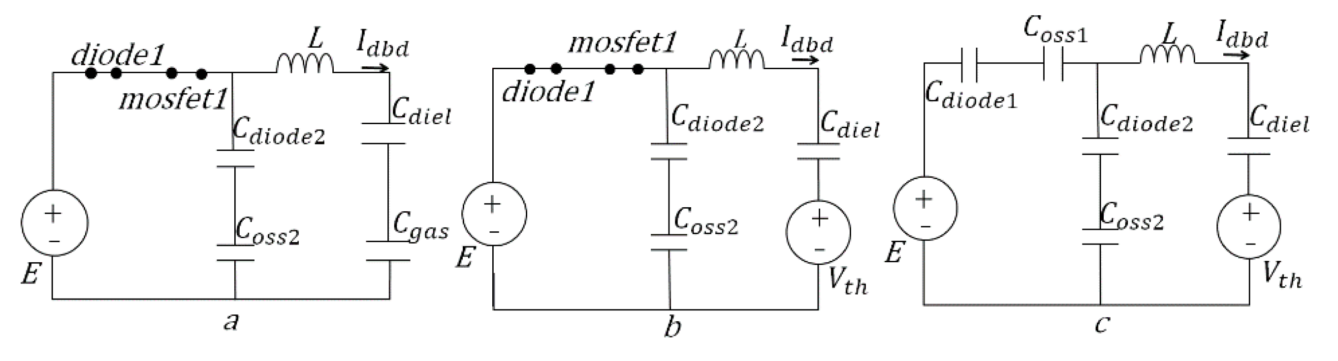
In the following part of this document, the influence of the semiconductors’ parasitic capacitance is considered. The equivalent circuit for each stage (Figure 3) must be modified, as shown in Figure 7. The positive current pulse is equivalent to circuits (a) and (b). Th1 is turned ON (MOSFET1 is closed) and diode1 is conducting; MOSFET2 and diode2 are OFF. Current flows from the DC power supply to the DBD. The DC high voltage (HV) source imposes the voltage across semiconductors capacitances. Therefore, during DBD conduction, the capacitances of MOSFET2 and diode2, seeing a DC voltage, cannot shunt the discharge current.
In a second phase, the DBD current goes to zero, the discharge turns OFF, diode1 blocks spontaneously and (after a short delay to guarantee ZCS turn OFF) MOSFET1 is switched OFF. At this time, the MOSFET2 and diode2 voltages are freed; all switches are OFF and a charge transfer takes place between Cdiode1, Cdiode2, Coss1, Coss2 and Ceq (Figure 7c). As shown in Figure 6, when the DC HV supply does not impose the voltage on the open thyristor, oscillations appear. They cause over-voltage across the semiconductors.
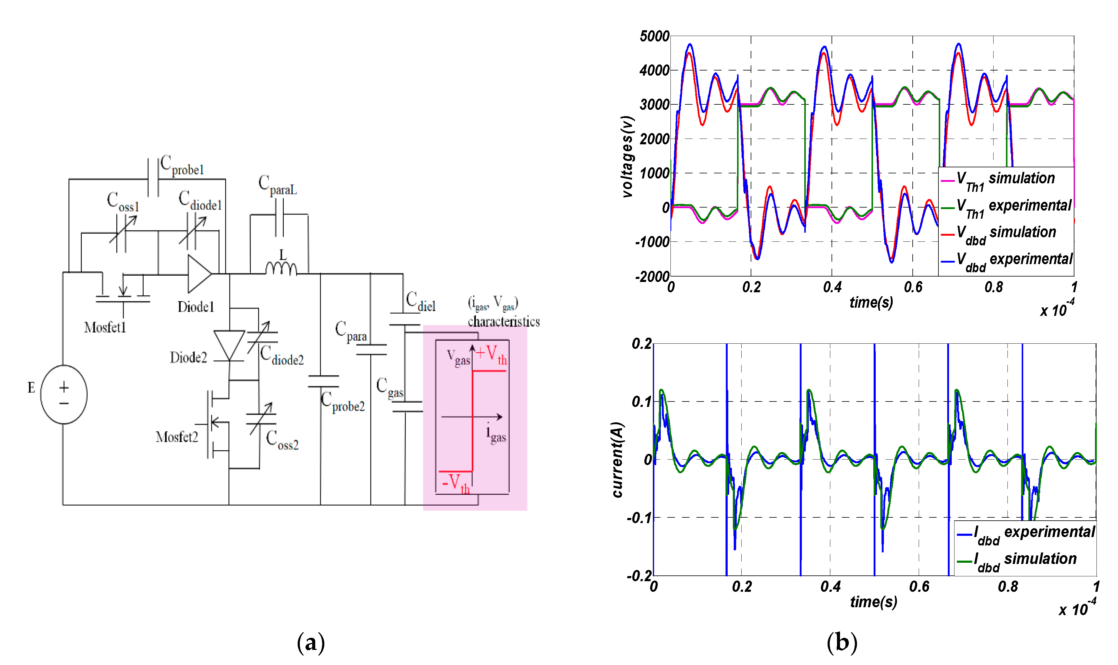
A comparison between the experimental measurements and simulation results, using PLECS [26] (PLEXIM, Zürich, Switzerland), is given in Figure 8. The parasitic capacitances are identified as follows: The inductance is characterized by an impedance bridge. The nonlinear parasitic capacitance, Coss for the MOSFETs and diodes are taken from CREE data sheets and arranged in tables indexed by semiconductor voltage. Cpara is the parasitic capacitance of the high-voltage connection to the DBD apparatus with respect to the ground; it is experimentally measured when the discharge is OFF.
As seen in Figure 8b, experimental and simulated waveforms match, with a very good level of accuracy. Oscillations have the same frequency; in addition, DBD and switch voltages are very similar. Owing to a very simple electrical model of the discharge, a small difference remains at the idbd current when the discharge is ignited. We now consider that this model accurately depicts the actual device. If the capacitance of the semiconductors is removed from the simulation, no oscillation occurs (data not shown). Therefore, the semiconductors are definitely responsible for this oscillation. In this topology, if the half period is close to the discharge current conduction (meaning that ∆Tblank as seen in Figure 2. is almost null), oscillation is minimized. Therefore, an accurate modification of the switching frequency could be a solution for reducing the oscillations associated with the semiconductor parasitic capacitance.
3.3. Power Balance
In order to prevent any risk of destruction to the high-voltage MOSFETs, and due to the oscillations presented above, the voltage applied by the HV DC supply E is limited to 4 kV. The converter performances are estimated and are presented in Figure 9. The power injected into the DBD device is measured with a traditional Q-V plot [22] (the energy transferred during one operating cycle is computed as the surface delimited by the Q-V plot). Power dissipation in the MOSFET is measured using a thermal method [31] and loss estimation is also provided using the simulation model. Obviously, the loss levels in the 10 kV MOSFETs seriously limit the efficiency of this converter.
In Figure 9, the power injected into the DBD and the power lost in the two MOSFETs are plotted as a function of the E voltage at f = 60 kHz operating frequency. This figure shows that power delivered to the DBD can rise up to 400 W. The DC high-voltage power supply (E on the previously presented circuits) cannot provide voltages beyond 3.6 kV, indeed, our power supply is limited in current. It indirectly implies a limitation on the power. In the condition presented in Figure 8, this limitation is reached at 3.6 kV. For another DBD, the current limitation can be reached for higher or lower voltage. An efficiency of 60% is obtained at this point and it seems that it would be higher if the E voltage could be increased. Below E = Vdbd = 2.6 kV, the discharge is never ignited, therefore, all the power is dissipated in the MOSFETs. The voltage across the switches is measured just before turn ON and the switching losses are calculated, with the energy stored in the COSS, using the capacitance value that is given by the constructor (232 pF), via the following formula: Switching losses = f.COSS.V2MOSFET.
These calculated losses are very close to the measured total ones, and thus represent a very high percentage of the total losses. These loss levels are particularly consistent with the results obtained in previous works, with the same semiconductor devices [20,28] (although probably from an older generation).
4. Discussion
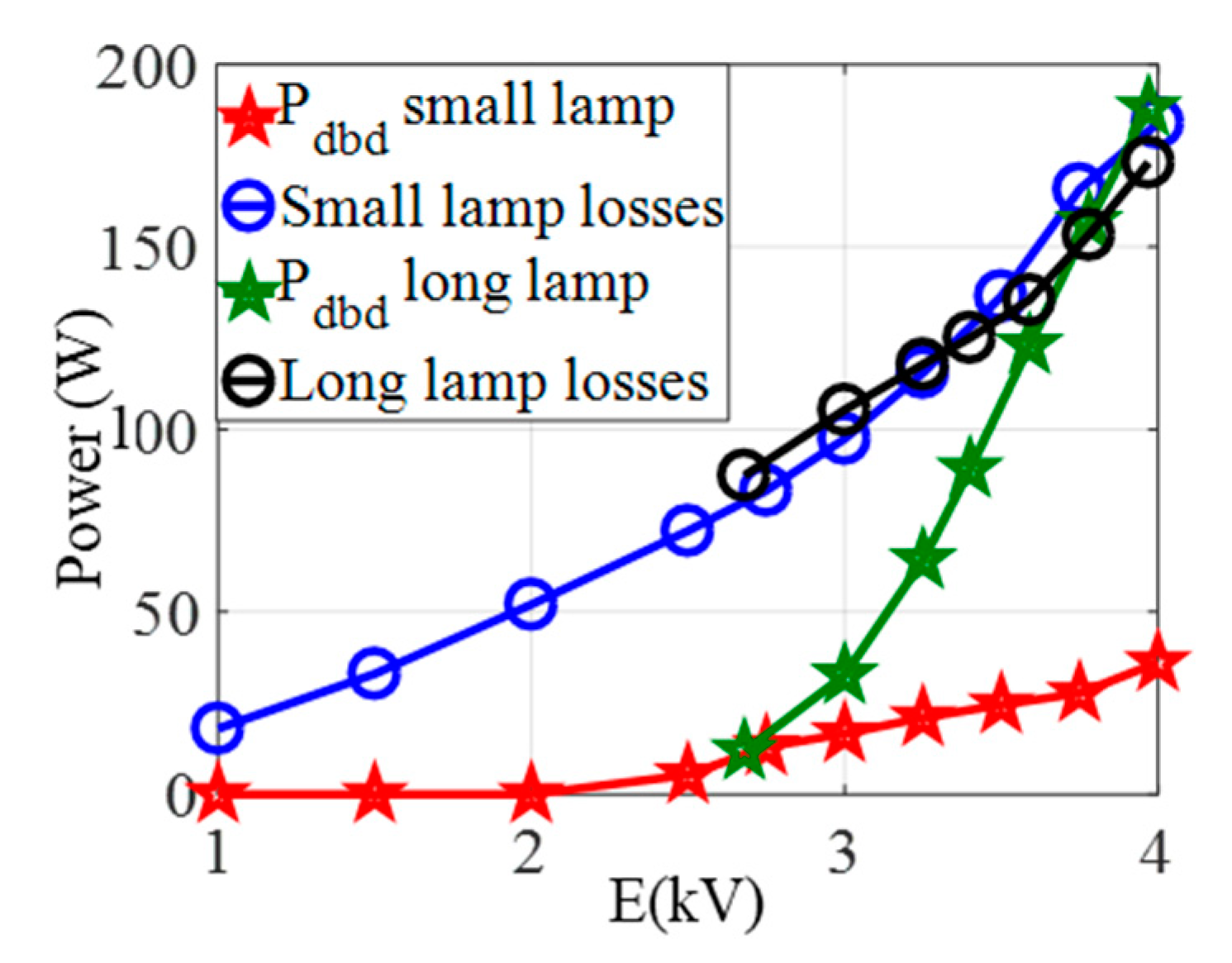
To point out the dependence between the losses and the current transferred to the lamp, we compare the performances obtained with the original bulb (60 cm) and with a shorter (15 cm) lamp, the latter can be seen in Figure 5b and it has the same diameter and the same material as those studied in the first part of this paper. Therefore, the breakdown voltage is not changed, and only the equivalent capacitance of the lamp Cgas and Cdiel are modified. The surface in contact with the discharge being lower, current and power transferred to the lamp are lower. In Figure 10, we show the comparison between the small and the long lamp, concerning the transferred power and MOSFETs’ losses.
As expected, power transferred to the small lamp is lower than that transferred to the long lamp. Interestingly, losses in the power supply present the same value for the both lamps. Consequently, for the same breakdown voltage, current transferred to the discharge does not change losses in the power supply. It is consistent with the observation that the majority of losses is MOSFETs’ turn-ON losses, due to the dissipation of the energy stored in Coss. For a given switch, they depend only on V+dbd, the voltage applied across the switch at turn ON, which rises with the applied voltage E.
Therefore, these switches should be used with a high power DBD. We can conclude that this topology is fitted for a DBD with a small gap (to have relatively low breakdown voltage Vth) and a large area. Here, we work with the lamp having the largest area for a cylindrical configuration, available in our laboratory.
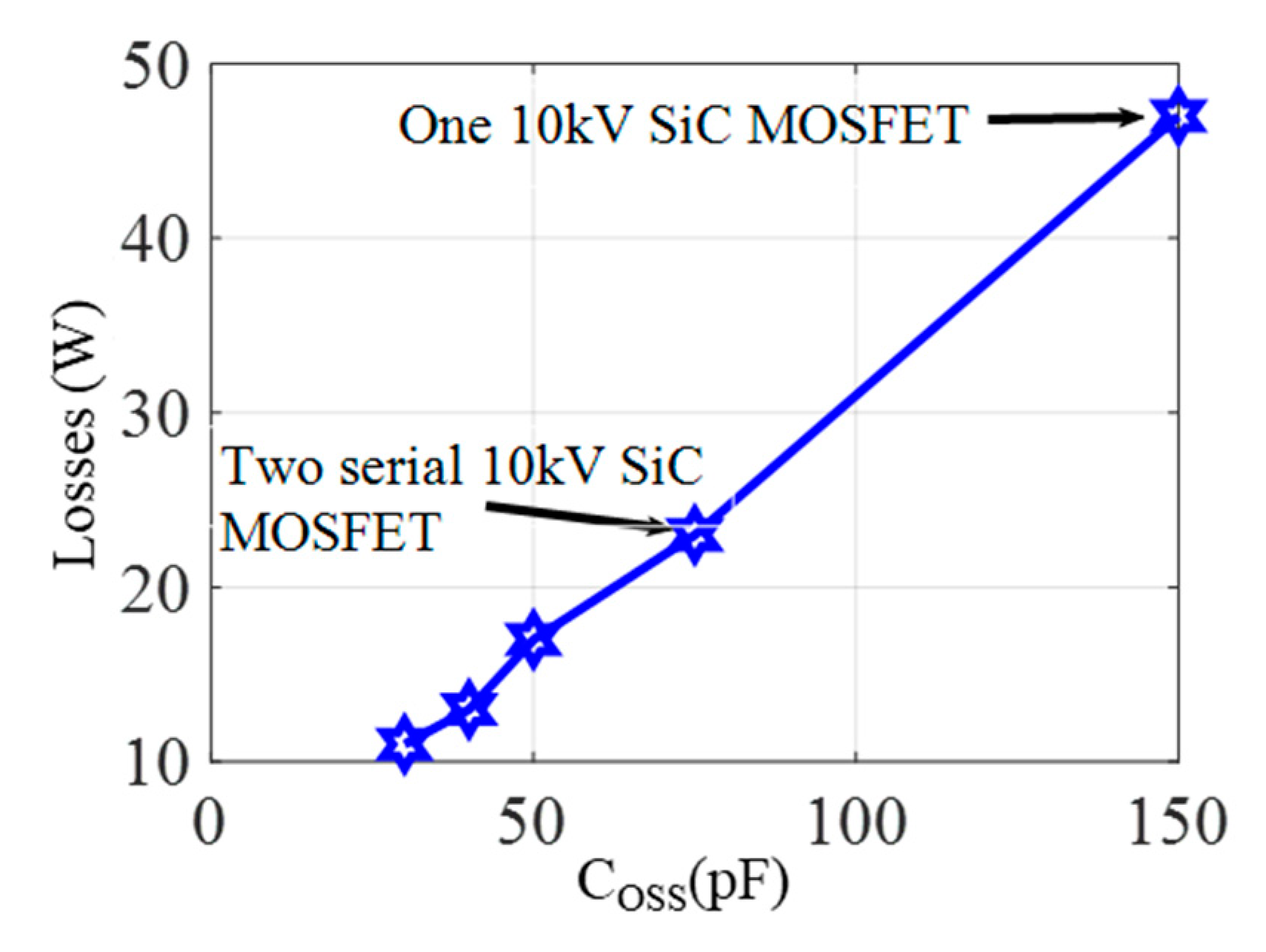
To understand and to try to limit this very high percentage of losses due to the MOSFETs’ Coss, a simulation of the whole system (static converter + DBD device) is performed. It shows that the conduction losses are negligible (less than 1 W). The results of this simulation are consistent with the experiment presented above. As shown in Figure 11, the MOSFET losses directly depend on the intrinsic capacitance of these semiconductors. In addition, according to the selected topology, these turn-ON losses are also proportional to the switching frequency, PturnON = k.f.Coss.E2. In the study previously presented in [27], we showed that all the parasitic capacitances (inductance, voltage probes, diodes, and MOSFET) modified the theoretical value of the transferred power, and that taking advantage of the latter to improve the performances was a possible option. Nevertheless, this was a marginal optimization and power balance point of view needed to be considered. Our present experimental results demonstrate that only the intrinsic capacitance of the MOSFET directly affects the efficiency. The other parasitic capacitances only change the voltage waveform as the frequency and the amplitude of the oscillations, when the discharge turn OFF.
The losses pointed out in Figure 10 are inherent to our application. Firstly, the E value cannot be drastically reduced, as sufficient voltage is required to ignite the DBD. Secondly, the frequency range is generally selected according to the dynamics of the chemical and physical mechanisms that take place in the plasma.
Currently, our lamp can receive several thousand Watts. The geometry (and therefore the relatively low capacitance) of our lamp requires a relatively low discharge current (#100 mA). SiC MOSFET used in this study is designed for relatively high current (10 A), whereas the peak current on the presented waveforms do not exceed 1 A, and high-power applications. For classical use of this SIC MOSFET, the turn-ON losses are acceptable. A MOSFET with the same voltage range but with a lower current rating would be more suitable for our case. Indeed, decreasing the current range requires decreasing the MOSFET chip area, and therefore the COSS capacitance. Consequently, turn-ON losses caused by the energy stored in the COSS intrinsic capacitance would be reduced.
In order to improve the efficiency of the system, many directions have been taken. The topology can be modified in order to obtain the zero voltage switching (ZVS) condition, therefore, canceling turn-ON losses. The value of the Coss intrinsic capacitance must be reduced. Several solutions are possible for this purpose. The first one is do design a 10 kV MOSFET with a lower Coss, as explained above. This kind of component is unfortunately currently unavailable, and we can assume that the high-voltage/low-current applications (as DBD) are not numerous enough to envisage an industrial development of such a device. A more realistic possibility is to connect MOSFETs in series, as it is done in a commercial switch [18]. Figure 11 shows the calculated losses with one 10 kV SiC MOSFET and also losses with two 10 kV SiC MOSFET in series. However, in a series connection, the voltage is distributed between the whole components set. MOSFETs with a lower voltage rating and a lower Coss could be used [27]. It is important to note that this solution implies an efficient voltage balance of the MOSFETs.
5. Conclusions
The transformerless topology, presented in this paper, has shown to be able to ignite a DBD lamp and to efficiently control the power transferred to the bulb. This first point demonstrates the feasibility of using the available 10 kV SiC MOSFETs to supply a DBD UV lamp, with the usual power level (generally achieved with a transformer in the power chain). The main advantage of this converter is its transformerless operation, with a reduced number of switches (only two). Moreover, with the presented topology, thanks to the inductance directly connected to the DBD, the parasitic capacitance does not directly affect the OFF time and so the behavior of the discharge.
Nevertheless, this topology raises the issue of MOSFET’s intrinsic capacitance. Firstly, this capacitance can cause oscillations, and then overvoltage at the switches terminals when the discharge extinguishes. Secondly, intrinsic capacitance Coss, due to the energy stored there before turn ON, causes significant losses in the MOSFETs.
These losses are a drawback when using the 10 kV SiC MOSFETs presented in this study. However, several solutions can be implemented to use this semiconductor. Firstly, series connection of those 10 kV SiC MOSFETs dividing the equivalent Coss, and thus reducing the losses, have shown to be advantageous for the improvement of the system’s efficiency. Moreover, this solution allows the system to sustain a higher voltage. Secondly, the selected SiC MOSFETs can profitably be considered, provided the power transmitted to the DBD is sufficiently high. It implies generally to consider a DBD with a large surface.
Generally speaking, concerning applications of DBD, the single-chip SiC MOSFET technology which was used in the proposed topology is rather restricted to the niche market of high power DBD, until there is a lower current rating (and lower intrinsic capacitance) transistor available.
Author Contributions
Validation, simulation, experimentation mainly realized by M.A.D. and A.B.; methodology, writing mainly by H.P. All authors have read and agreed to the published version of the manuscript.
Funding
This research received no external funding.
Acknowledgments
Part of this study is in the framework of French-Colombian cooperation, with the support of the ECOS program (ECOS Nord, COLCIENCIAS-ICETEX).
Conflicts of Interest
The authors declare no conflict of interest.
References
- Kogelschatz, U. Dielectric-Barrier Discharges: Their History, Discharge Physics, and Industrial Applications. Plasma Chem. Plasma Process. 2003, 23, 1–46. [Google Scholar] [CrossRef]
- Lomaev, M.I.; Skakun, V.; Sosnin, E.A.; Tarasenko, V.F.; Shitts, D.; Erofeev, M.V. Excilamps: Efficient sources of spontaneous UV and VUV radiation. Uspekhi Fiz. Nauk. 2003, 173, 201. [Google Scholar] [CrossRef]
- Massines, F.; Sarra-Bournet, C.; Fanelli, F.; Naudé, N.; Gherardi, N. Atmospheric Pressure Low Temperature Direct Plasma Technology: Status and Challenges for Thin Film Deposition. Plasma Process. Polym. 2012, 9, 1041–1073. [Google Scholar] [CrossRef]
- Corke, T.; Post, M.L.; Orlov, D.M. Single dielectric barrier discharge plasma enhanced aerodynamics: Physics, modeling and applications. Exp. Fluids 2008, 46, 1–26. [Google Scholar] [CrossRef]
- Ordìz, C.; Alonso, J.M.; Costa, M.A.D.; Ribas, J.; Calleja, A.J. Development of a high-voltage closed-loop power supply for ozone generation. In Proceedings of the 2008 Twenty-Third Annual IEEE Applied Power Electronics Conference and Exposition, Austin, TX, USA, 24–28 February 2008. [Google Scholar] [CrossRef]
- Meisser, M.; Kling, R.; Heering, W. Universal resonant topology for high frequency pulsed operation of Dielectric Barrier Discharge light sources. In Proceedings of the 2011 Twenty-Sixth Annual IEEE Applied Power Electronics Conference and Exposition (APEC), New York, NY, USA, 6–11 March 2011; pp. 1180–1187. [Google Scholar]
- Diez, R.; Piquet, H.; Cousineau, M.; Bhosle, S. Current-Mode Power Converter for Radiation Control in DBD Excimer Lamps. IEEE Trans. Ind. Electron. 2011, 59, 1912–1919. [Google Scholar] [CrossRef] [Green Version]
- Diez, R.; Piquet, H.; Florez, D.; Bonnin, X. Current-Mode Approach in Power Supplies for DBD Excilamps: Review of 4 Topologies. IEEE Trans. Plasma Sci. 2014, 43, 452–460. [Google Scholar] [CrossRef] [Green Version]
- Bonnin, X.; Piquet, H.; Diez, R.; Florez, D. Designing the high voltage transformer of power supplies for DBD: Windings arrangment to reduce the parasitic capacitive effects. In Proceedings of the 15th European Conference on Power Electronics and Applications (EPE), Lille, France, 2–6 September 2013; pp. 1–9. [Google Scholar]
- Bonnin, X.; Piquet, H.; Naudé, N.; Bouzidi, M.C.; Gherardi, N.; Blaquière, J.-M. Design of a current converter to maximize the power into homogeneous dielectric barrier discharge (DBD) devices. Eur. Phys. J. Appl. Phys. 2013, 64, 10901. [Google Scholar] [CrossRef] [Green Version]
- Meisser, M.; Rainer, K.; Wolfgang, H. Transformerless high voltage pulse generators for bipolar drive of Dielectric Barrier Discharges. In Proceedings of the PCIM 2011, Nuremberg, Germany, 17–19 May 2011. [Google Scholar]
- Bonnin, X.; Brandelero, J.; Videau, N.; Piquet, H.; Meynard, T. A High Voltage High Frequency Resonant Inverter for Supplying DBD Devices with Short Discharge Current Pulses. IEEE Trans. Power Electron. 2013, 29, 4261–4269. [Google Scholar] [CrossRef] [Green Version]
- Gas Discharge Closing Switches; Springer Science and Business Media LLC: Berlin/Heidelberg, Germany, 1990.
- Cheng, X.; Huang, B.; Zhang, C.; Kong, F.; Luo, Z.; Shao, T. A Nanosecond Pulsed Generator With Fast-Solid-State Switch for Synchronous Discharge in Plasma Synthetic Jet Actuators. IEEE Trans. Plasma Sci. 2019, 47, 1901–1908. [Google Scholar] [CrossRef]
- Lu, X.; Laroussi, M. Dynamics of an atmospheric pressure plasma plume generated by submicrosecond voltage pulses. J. Appl. Phys. 2006, 100, 63302. [Google Scholar] [CrossRef] [Green Version]
- Judée, F.; Wattieaux, G.; Yousfi, M.; Merbahi, N. Analysis of Ar plasma jets induced by single and double dielectric barrier discharges at atmospheric pressure. J. Appl. Phys. 2016, 120, 114901. [Google Scholar] [CrossRef]
- Laurent, M.; Desjardins, E.; Meichelboeck, M.; Belinger, A.; Naudé, N.; Stafford, L.; Gherardi, N.; Laroche, G. Influence of a square pulse voltage on argon-ethyl lactate discharges and their plasma-deposited coatings using time-resolved spectroscopy and surface characterization. Phys. Plasmas 2018, 25, 103504. [Google Scholar] [CrossRef]
- Behlke, F. MOSFET-Type High-Voltage Switch with Extremely Short Switching Time. German Patent DE3630775A1, 9 October 1986. [Google Scholar]
- El-Deib, A.; Dawson, F.; Zissis, G. Transformer-Less current controlled driver for a dielectric barrier discharge lamp using HV silicon carbide (SiC) switching devices. IEEE Energy Convers. Congr. Expo. 2011. [Google Scholar] [CrossRef]
- Wang, J.; Zhao, T.; Li, J.; Huang, A.Q.; Callanan, R.; Husna, F.; Agarwal, A. Characterization, Modeling, and Application of 10-kV SiC MOSFET, Electron Devices. IEEE Trans. 2008, 55, 1798–1806. [Google Scholar] [CrossRef]
- Diop, M.A.; Belinger, A.; Piquet, H. DBD transformerless power supplies: Impact of parasitic capacitances on power transfer. J. Phys. Conf. Ser. 2017, 825, 012004. [Google Scholar] [CrossRef]
- Mirzaee, H.; De, A.; Tripathi, A.; Bhattacharya, S. Design Comparison of High-Power Medium-Voltage Converters Based on a 6.5-kV Si-IGBT/Si-PiN Diode, a 6.5-kV Si-IGBT/SiC-JBS Diode, and a 10-kV SiC-MOSFET/SiC-JBS Diode. IEEE Trans. Ind. Appl. 2014, 50, 2728–2740. [Google Scholar] [CrossRef]
- Manley, T.C. The Electric Characteristics of the Ozonator Discharge. Trans. Electrochem. Soc. 1943, 84, 83. [Google Scholar] [CrossRef]
- Díez, R.; Salanne, J.-P.; Bhosle, S.; Piquet, H.; Zissis, G. Predictive model of a DBD lamp for power supply design and method for the automatic identification of its parameters. Eur. Phys. J. Appl. Phys. 2007, 37, 307–313. [Google Scholar] [CrossRef]
- Cousineau, M.; Diez, R.; Piquet, H.; Durrieu, O. Synthesized High-Frequency Thyristor for Dielectric Barrier Discharge Excimer Lamps. IEEE Trans. Ind. Electron. 2011, 59, 1920–1928. [Google Scholar] [CrossRef] [Green Version]
- PLECS. Simulation Platform for Power Electronic Systems. Available online: http://www.plexim.com/plecs (accessed on 17 July 2020).
- Chéron, Y. Soft Commutation; Chapman & Hall: London, UK, 1992. [Google Scholar]
- Pala, V.; Brunt, E.V.; Cheng, L.; O’Loughlin, M.; Richmond, J.; Burk, A.; Allen, S.T.; Grider, D.; Palmour, J.W.; Scozzie, C.J. 10 kV and 15 kV silicon carbide power MOSFETs for next-generation energy conversion and transmission systems. In 2014 IEEE Energy Conversion Congress and Exposition (ECCE), Pittsburgh, PA, USA, 14–18 September 2014; Institute of Electrical and Electronics Engineers (IEEE): New York, NY, USA, 2014; pp. 449–454. [Google Scholar]
- Hess, H.L.; Baker, R.J. Transformerless Capacitive Coupling of Gate Signals for Series Operation of Power MOS Device. IEEE Trans. Power Electron. 2000, 15, 923–930. [Google Scholar] [CrossRef]
- ALTERA DE0 Nano User Manual. Available online: https://www.terasic.com.tw/attachment/archive/941/DE0-Nano-SoC_User_manual.pdf (accessed on 17 July 2020).
- Viswanathan, K.; Oruganti, R. Evaluation of Power Losses in a Boost PFC Unit by Temperature Measurements. IEEE Trans. Ind. Appl. 2007, 43, 1320–1328. [Google Scholar] [CrossRef]
Figure 1.
(a) Lamp model—blue background, and (b) proposed current-controlled source to supply the dielectric barrier discharge (DBD)—green background.
Figure 1.
(a) Lamp model—blue background, and (b) proposed current-controlled source to supply the dielectric barrier discharge (DBD)—green background.

Figure 2.
(a) Theoretical Idbd, current and Vdbd, Vdiel, and Vgas voltages; (b) Synthesized thyristors.
Figure 2.
(a) Theoretical Idbd, current and Vdbd, Vdiel, and Vgas voltages; (b) Synthesized thyristors.

Figure 3.
The six operating stages—to be observed on the waveforms of Figure 2a. + positive current pulse. (a) Th1 is turned ON (plasma being OFF); (b) Vgas voltage has reached Vth and the plasma is ON; (c) End of the positive current pulse. Idbd, has reached the 0 level and Th1 has spontaneously turned OFF. + negative current pulse, (d) Th2 is turned ON (plasma being OFF); (e) Vgas voltage has reached, Vth and the plasma is ON; (f) End of the positive current pulse. Idbd, has reached the 0 level and Th2 has spontaneously turned OFF. Background colors of Figure 3 are directly linked to the corresponding colors/periods of Figure 2. (a): blue, when the current pulses have started, but the plasma is still OFF (a and d), pink, during the time the plasma is ON (b and e), green during the idle time (plasma is OFF and there is no current pulse, c and f).

Figure 4.
Theoretical current and voltage in thyristors, MOSFETs, inductance, and DBD.

Figure 5.
Experimental setups. (a) Schematic of the setup with voltage and current probes, the photo is the long DBD lamp when plasma is ignited (250 W); (b) Picture of the experimental setup connected to the short DBD lamp in the rear part and MOSFET board in the front part. The solid lines correspond to the power wires, the dashed lines to the measurement wires.

Figure 6.
Experimental measurements, showing the effect of the MOSFET parasitic capacitances, E = 3.5 kV, f = 60 kHz.
Figure 6.
Experimental measurements, showing the effect of the MOSFET parasitic capacitances, E = 3.5 kV, f = 60 kHz.

Figure 7.
Operating conditions with parasitic capacitances. (a) Before the breakdown (current flows through diode1 and MOSFET 1); (b) During the discharge (gas voltage is equal to Vth); (c) After the discharge and after Th1 opening (current flows through the parasitic capacitance of diode 1 and MOSFET 1).

Figure 8.
Simulation model. (a) Experimental and measured waveforms, E = 4 kV, f = 30 kHz; (b) Switch and DBD voltage on the top plot, DBD current on the bottom plot.
Figure 8.
Simulation model. (a) Experimental and measured waveforms, E = 4 kV, f = 30 kHz; (b) Switch and DBD voltage on the top plot, DBD current on the bottom plot.

Figure 9.
Discharge power and loss in one MOSFET, versus the high voltage (HV) DC supply’s voltage E, f = 60 kHz.
Figure 9.
Discharge power and loss in one MOSFET, versus the high voltage (HV) DC supply’s voltage E, f = 60 kHz.

Figure 10.
Comparison between the smaller and the longer lamp. Frequency = 30 kHz.

Figure 11.
Simulated losses for one MOSFET versus Coss. Operating conditions, E = 3 kV and f = 30 kHz.
Figure 11.
Simulated losses for one MOSFET versus Coss. Operating conditions, E = 3 kV and f = 30 kHz.


Table 1.
Duration of gas operating sequences and switches voltage stresses.
| Op. Stage | Switches States | Gas State | Stage Duration 1 | Vdbd Voltage Peak Value |
|---|---|---|---|---|
| (a) | Th1 ON, Th2 OFF | OFF | and | |
| (b) | Th1 ON, Th2 OFF | ON |
1 With: , E being the DC voltage source magnitude.
Table 2.
Electrical parameters of the XeCl DBD lamps and the converter.
| Vth | Cdiel | Cgas | Supply | ||
|---|---|---|---|---|---|
| Long bulb (60 cm) | 1310 V | 373 pF | 123 pF | L | f |
| Short bulb (15 cm) | 1310 V | 85 pF | 30 pF | 4 mH | 10–70 kHz |
© 2020 by the authors. Licensee MDPI, Basel, Switzerland. This article is an open access article distributed under the terms and conditions of the Creative Commons Attribution (CC BY) license (http://creativecommons.org/licenses/by/4.0/).
Share and Cite
MDPI and ACS Style
Diop, M.A.; Belinger, A.; Piquet, H. 10 kV SiC MOSFET Evaluation for Dielectric Barrier Discharge Transformerless Power Supply. Plasma 2020, 3, 103-116. https://0-doi-org.brum.beds.ac.uk/10.3390/plasma3030009
AMA Style
Diop MA, Belinger A, Piquet H. 10 kV SiC MOSFET Evaluation for Dielectric Barrier Discharge Transformerless Power Supply. Plasma. 2020; 3(3):103-116. https://0-doi-org.brum.beds.ac.uk/10.3390/plasma3030009
Chicago/Turabian StyleDiop, Mame Andallah, Antoine Belinger, and Hubert Piquet. 2020. "10 kV SiC MOSFET Evaluation for Dielectric Barrier Discharge Transformerless Power Supply" Plasma 3, no. 3: 103-116. https://0-doi-org.brum.beds.ac.uk/10.3390/plasma3030009