Fermi Level Engineering for Large Permittivity in BaTiO3-Based Multilayers
by
 ,
,
Christopher Castro Chavarría
1,2,*, 
Sandrine Payan
1,
Jean-Paul Salvetat
3,
Mario Maglione
1 and
Andreas Klein
2 1
ICMCB, CNRS, Université de Bordeaux, UMR 5026, F-33600 Pessac, France
2
Department of Materials and Earth Sciences, Electronic Structure of Materials, Technische Universität Darmstadt, Otto-Berndt-Str. 3, 64287 Darmstadt, Germany
3
PLACAMAT, CNRS, Université de Bordeaux, UMS 3626, F-33600 Pessac, France
*
Author to whom correspondence should be addressed.
Surfaces 2020, 3(4), 567-578; https://0-doi-org.brum.beds.ac.uk/10.3390/surfaces3040038
Submission received: 9 September 2020
/
Revised: 29 September 2020
/
Accepted: 30 September 2020
/
Published: 5 October 2020
Abstract
:Multilayered doped BaTiO3 thin films have been fabricated by physical vapor deposition (PVD) on low-cost polycrystalline substrates with the aim to improve dielectric properties by controlling point charge defects at the interfaces. We show that carefully designed interfaces lead to increasing the relative permittivity of the BaTiO3 thin films, in contradiction with the common belief that interfaces behave as dead layers. High relative permittivity up to 1030 and tanδ = 4% at 100 kHz and room temperature were obtained on BaTiO3 multilayered films deposited on Si/Pt substrates by PVD. The large permittivity is suspected to be an extrinsic contribution due to band bending at the interfaces, as inferred by in-situ X-ray photoelectron spectroscopy. A 20-nm depletion layer was found to be associated with an interdiffusion of dopants, as measured by depth profiling with time-of-flight secondary ion mass spectrometry. The films exhibit high permittivity and low dielectric losses stable between 200 and 400 K, which meet the requirement of electronic applications.
1. Introduction
Polycrystalline BaTiO3 (BTO) usually loses its main properties when deposited as thin films. Much lower permittivity than in bulk and no clear phase transition are often observed as a result of random internal strain induced by the deposition process, lattice expansion mismatch, or (local) variation of stoichiometry. Deep investigations since the mid-nineties have shown that restoring the polarization and dielectric properties in BaTiO3 (BTO) thin films requires advanced processes. The microstructure of thin films can span from granular as in chemical solution deposited films [1,2] to epitaxial as in Molecular Beam Epitaxy (MBE) [3,4] and Pulsed Laser Deposition (PLD) grown films [5,6] for a large variety of substrates. In many instances, dielectric, polarization and piezoelectric properties may be recovered, sometimes thanks to the substrate-induced stress on the films. Restored dielectric permittivity and losses, however, may suffer from stability issues versus temperature or stress changes, which is detrimental for many applications. The scope of the present paper is to use artificially charged interfaces in BaTiO3 multilayers to stabilize large dielectric permittivity in integrated 300-nm-thick structures deposited on Si/Pt substrates.
Interface control in ferroelectric materials is a long-standing issue needing a deeper understanding, mostly about the interplay between point charge defects and interfaces.
Back in the seventies, donor doping (La, Nb) in BaTiO3 ceramics resulted in spectacular resistance changes, which were modelled using grain boundary band bending [7]. From the mid-nineties, large and extrinsic dielectric permittivities have been reported in a large variety of bulk polycrystalline materials, all explained using space charge or Maxwell–Wagner models [8,9,10,11] without microscopic insight into the actual interfaces. Here, to achieve interface control, we have combined charged point defect substitution (Mn, Nb, La) in BaTiO3 thin films and multilayer architectures. We first show that the Fermi level in individual films may be tuned from very close to the conduction band in reduced (VO) or donor-doped films (La, Nb) to the mid-gap under acceptor-doping (Mn). Stacking these films induced band bending over more than 10 nm in La/Nb and in Mn/Nb stacks as evidenced by X-ray photoelectron spectroscopy, which was performed in situ along stepwise interface formation. In the case of La/Nb interfaces this unusual band bending induced large dielectric permittivity of more than 1000 together with moderate losses of less than 5% and temperature stability over more than 100 K. We then linked these appealing dielectric parameters and band bending to cross-diffusion of dopants between the layers. This cross-diffusion has been directly evidenced by time-of-flight secondary ion mass spectroscopy (TOF-SIMS) depth profiling. The cross-diffusion takes place over more than 10 nm in the case of Nb and La, which is very large. These heterostructures are one example of how band bending and free charge accumulation can artificially increase the effective dielectric permittivity while moderating dielectric losses and leakage currents. Unlike polycrystalline bulk materials, multilayers offer an efficient platform for understanding the origin of artificially enhanced permittivity using in situ X-ray photoelectron spectroscopy (XPS) and TOF-SIMS on the same samples.
2. Materials and Methods
Films were deposited by magnetron sputtering from home-made targets including the required amount of dopants. Target compositions as well as sputtering conditions are reported in Table 1. We used sputtering parameters and chambers as reported in our former investigations [12,13,14]. The different multilayers were deposited as 3 layers alternating between Mn-, Nb- or La-doped BaTiO3. We chose 5, 10 and 20 nm of Mn- or La-doped layers as top and bottom layers and 290, 280 and 260 nm of an Nb core layer, respectively, hence conserving a total thickness of 300 nm for each sample. In doing so, we expected that properties would not vary between the different stacks if only interfaces play a significant role. These heterostructures will be referred to as MNM5, MNM10 and MNM20. With the same approach, samples NMN20, LNL10 and NLN10 are heterostructures alternating between Nb (N), Mn (M) and La (L) with the thickness of the top and bottom layers at the end, always conserving a total of 300 nm (e.g., LNL10, is a sample with a 10-nm La bottom layer, a 280-nm Nb core layer and a 10-nm La top layer).
Substrates were pieces of silicon wafers covered by a platinum layer, which served as a bottom electrode for the electrical experiments and as ground to avoid charging in photoemission measurements. Crystallinity and phase purity were checked by (XRD) analysis, performed at room temperature on a PANalytical (Almelo, The Netherlands) X’pert MPD X’pert MPD-PRO Bragg-Brentano θ-θ geometry diffractometer using Cu Kα1,2 source. Since the amount of each substituted ion is less than 0.5% and because of line overlap with the major Ba or Ti ions, chemical analysis using Rutherford back scattering was not possible. We thus checked the additional contribution from the substituted heterovalent defects first by X-ray photoelectron spectroscopy (XPS) on single layers on a Physical Electronics PHI 5700 spectrometer at Darmstadt’s Integrated System for Material Science (DAISY-MAT) at Technische Universität Darmstadt (TU-Darmstadt), Germany [15]. On this system, we analyzed both in-situ and ex-situ samples. In-situ samples were XPS-probed directly after step-by-step deposition in a sputter deposition chamber connected to the analysis chamber. Ex-situ samples were processed in a sputtering chamber without direct connection to the XPS-chamber. These ex-situ samples were systematically treated prior to XPS measurement by heating to 400 °C in 0.5 Pa of 2 sccm O2 for 2 h in order to remove adsorbed pollutants. Chemical concentrations were obtained by integrating the peak surface of the main XPS lines (Ba 3d5/2, Ti 2p, O 1s and Nb 3d) and correcting them with their corresponding atomic sensitivity factors.
X-ray photoelectron spectroscopy was performed using a Physical Electronics PHI 5700 spectrometer (Chanhassen, MA, USA), which is part of the DAISY-MAT. Spectra are excited with monochromated Al Kα radiation and recorded with a takeoff angle of 45°. Binding energies are calibrated daily using the Fermi edge and Ag 3d5/2 emission of a cleaned Ag foil.
TOF-SIMS depth profiling experiments were performed using 1 keV Cs+ ions for sputtering and 30 keV Bi+ for analysis employing a TOF.SIMS 5 (IONTOF, Münster, Germany) at PLACAMAT, Pessac, France.
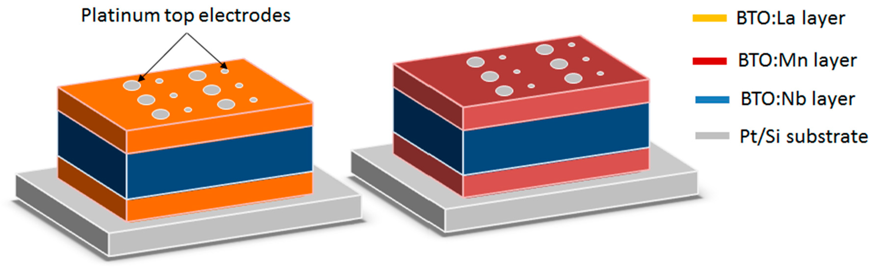
To measure dielectric permittivity (ε) and losses (tanδ), we sputtered platinum electrodes as 300- and 600-µm-diameter disks on top of 300-nm-thick BaTiO3 layers through a shadow mask as shown in Figure 1. In doing so, we were able to process 18 capacitors on 1 × 2 cm2 platinized silicon wafers.
3. Results and Discussion
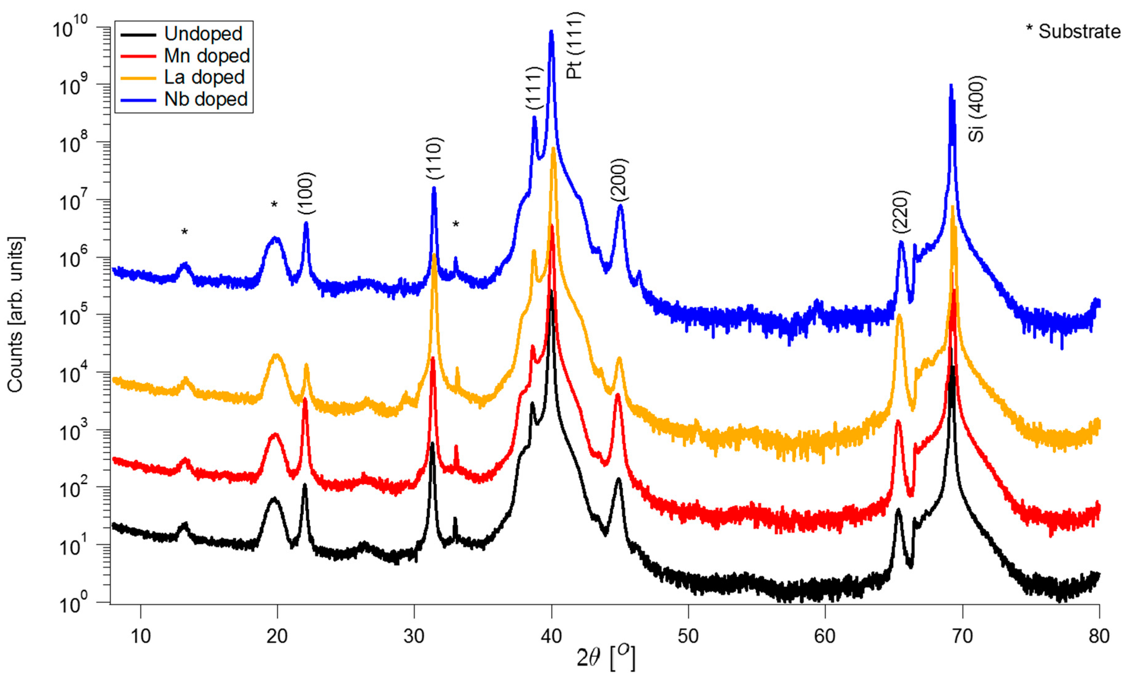
The microstructural properties of all thin films have been systematically analyzed by X-ray diffraction (XRD) in ϴ–2θ mode. XRD patterns of (un)doped single layer films are presented in Figure 2. All films present a polycrystalline perovskite structure without a preferential orientation or secondary phases in the detection limit of the probing technique. We did not find any significant shift nor preferential orientations with the insertion of dopants nor with the introduction of stacks (heterostructures). The overall chemical content and microstructure of the films is thus following our previous reports on similar systems [12,13].
The dielectric permittivity (ε) and losses (tanδ) at 100 kHz and room temperature (RT) of undoped, Mn-, La-, Nb-doped BaTiO3 films and heterostructures are reported in Table 2.
Dielectric permittivity and losses of undoped, Mn and La doped samples are comparable to those of other sputtered BaTiO3 films on Si/Pt substrates [12,16]. Nb doping induces a very large increase in ε due to electron charges generated by Nb5+/Ti4+ substitution, along with a well-defined band bending at the Pt electrode interfaces, as evidenced by XPS [17]. The interfacial space charge at the electrodes may also increase the effective dielectric permittivity as reported for BaTiO3 single crystals [18]. However, with Pt-electrode/oxide interfaces being hardly controlled, we decided to investigate internal interfaces generated by stacking several differently doped (Mn, La, Nb) BaTiO3 films.
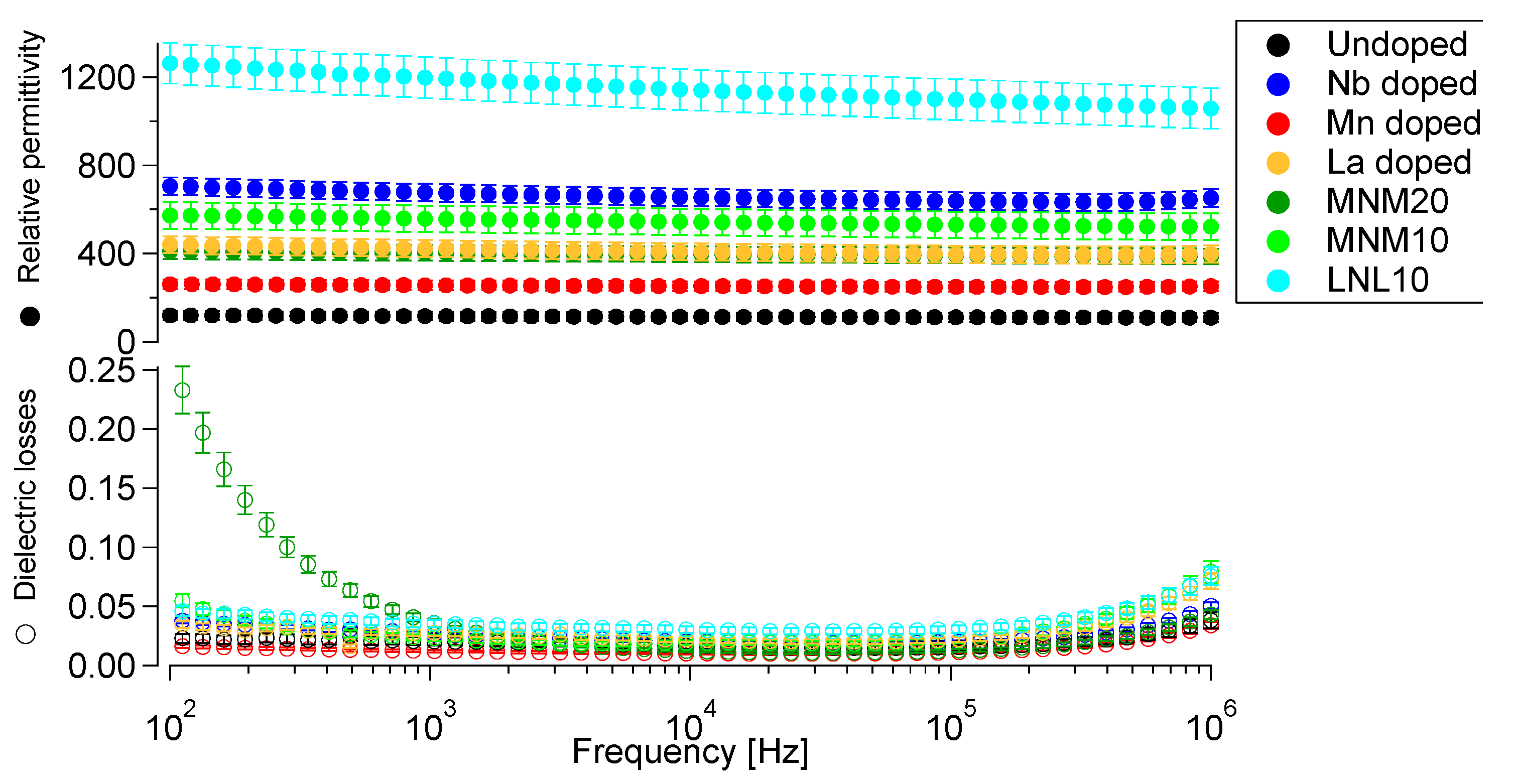
The prepared multilayer heterostructures consist mostly of one core layer embedded between two similar thin layers, keeping the total thickness at about 300 nm. In our notation, M, L, N stand for manganese-, lanthanum- and niobium-doped films, respectively, and the number following a given stack is the outer layer thickness. For example, MNM20 means a stack of a 260-nm-thick Nb-doped BaTiO3 film between two 20-nm Mn-doped layers. In a similar way as for single layers, we measured the dielectric permittivity and losses over 18 MIM capacitors on a single substrate. We also repeated the full process several times to confirm its reproducibility. RT dielectric parameters of several multilayers are reported in Table 2. A large increase in dielectric permittivity along with reasonably low losses was most pronounced for the LNL stacks (see Figure 3). The dielectric permittivity was mostly independent of temperature above 150 K, ruling out ferroelectric behavior, and was mostly independent of frequency (100Hz to 1MHz) at RT (see Figure 4). The absence of ferroelectric phase transition is common for sputtered polycrystalline BaTiO3 thin films [12,14,16,17,19]. It was also obvious that the dielectric permittivity of the stack was much higher than that of a series capacitor circuit modeling the 3 capacitive layers. This was a first evidence of an interfacial contribution to the dielectric permittivity of the stack.
To confirm this, we have analyzed the electronic structure of our films by XPS. First, a survey spectrum was used to identify the chemical elements present at the surface including possible contaminations. Second, we performed a high resolution measurement of the core levels of each element on their most intense peaks, in our case Ba 3d5/2, Ti 2p, O 1s and Ba 4d, in order to analyze oxidation states, surface composition and electronic structure. Finally, a detailed spectrum of the valence band was recorded, as the position of the valence band edge indicates the position of Fermi level, indicating the electrical nature of our semiconducting films given the known value (3.2 eV) of the bandgap [20]. Figure 5 shows a typical in-situ XPS routine analysis of an undoped BaTiO3 thin film.
In addition to this, EF-EVB can be obtained by measuring the core level binding energy ECL of any BaTiO3 core level as the difference EVB-ECL is a material constant. In this work, the value for EVB-ECL was determined by XPS in-situ measurements of the binding energies of the core levels Ba 3d, O 1s, Ti 2p and Ba 4d of several doped and undoped BaTiO3 thin films.
The low concentration of dopants made their detection by XPS difficult. The presence of La and Mn could not be confirmed, and only Nb XPS main line (3d5/2) showed up clearly, demonstrating that the Nb concentration was well above the XPS detection limit of about 0.1 at%. The presence of La and Mn was confirmed by TOF-SIMS. Doping BaTiO3 with donor dopants such as Nb and La should raise the Fermi level position closer to the conduction band [21,22]. This is indeed observed from the XPS binding energies of in-situ deposited layers. Nb-doped and La-doped films both show EF-EVB = 2.7 ± 0.1 eV and EF-EVB = 2.7 ± 0.1 eV, close to previous work 2.73 eV [12], while Mn-doped BaTiO3 thin films display EF-EVBM = 2.2 ± 0.1 eV.
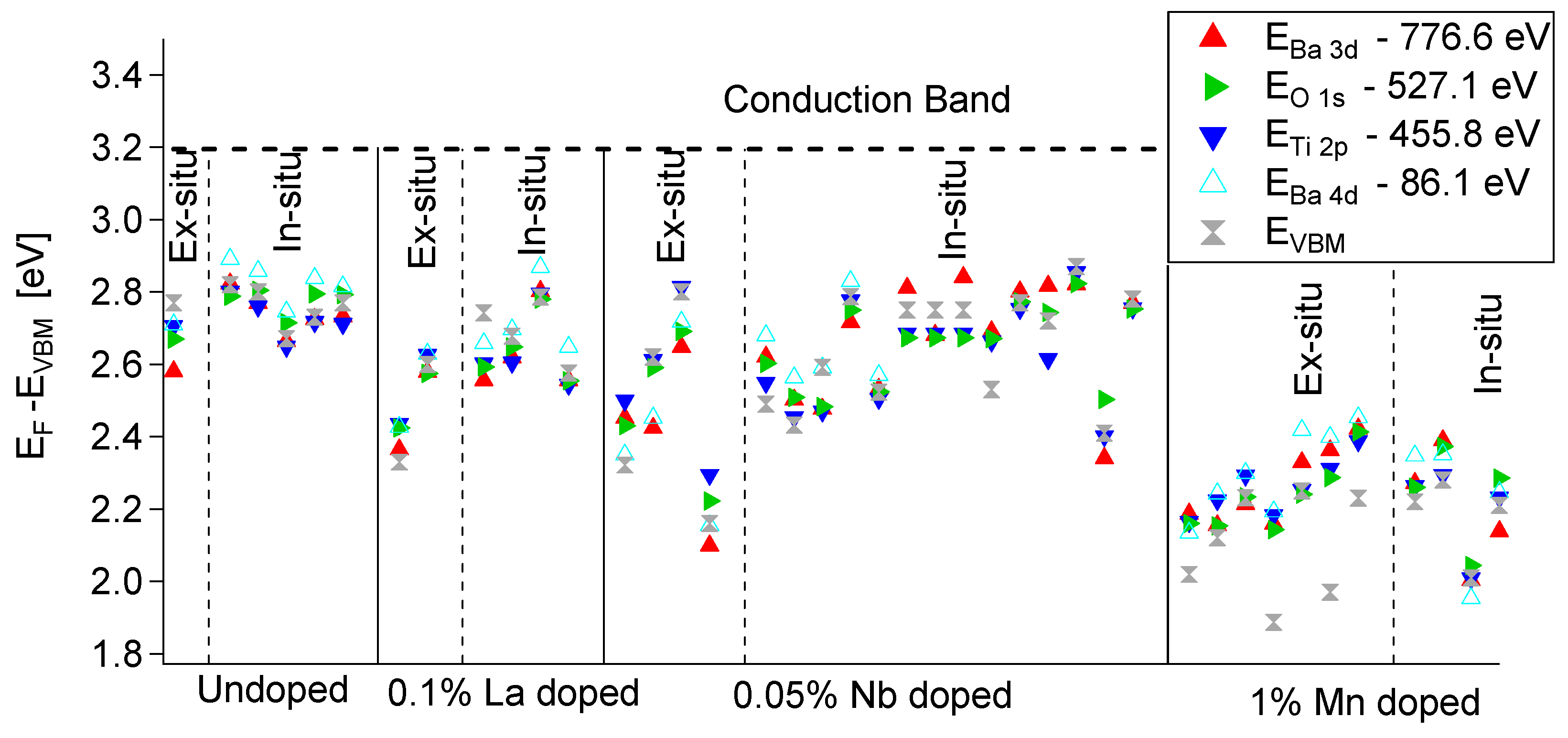
As several samples have been prepared outside DAISY-MAT, it is relevant to indicate the differences between ex-situ and in-situ samples. In Figure 6 we compare the Fermi energies of several BaTiO3 thin films, including the sample prepared at ICMCB (ex-situ) and those prepared at DAISY-MAT (in-situ).
The Fermi energies extracted from the core levels of the in-situ films are within 0.05 eV from the direct determination using the valence band maximum extrapolation [23] whereas the ex-situ films exhibit a larger scattering of 0.12 eV. This larger scattering of the ex-situ films may originate from a potential surface modification due to the cleaning procedure prior to the measurement. A Fermi level close to the conduction band results in a higher concentration of free electrons and, therefore, to a higher conductivity. In undoped films, the microstructure has a larger effect on the conductivity, as the columnar structure will increase the leakage currents compared to ceramics or single crystals. For the undoped samples, the EF is far from the conventional understanding of an insulator, that is to say, a mid-gap Fermi level position (1.6 eV above EVBM). This could be explained by the oxygen-poor atmosphere during deposition, creating a high concentration of oxygen vacancies that are compensated electronically, raising the EF closer to the conduction band. For the Mn-doped sample, EF obtained in this work is in accordance with the value found in the literature for the impurity transition level of Mn2+/3+ [24,25]. It is worth mentioning that due to the deposition conditions, we should be able to reach the second transition level, Mn3+/4+, by oxidizing treatments. The decrease in the Fermi level position within the band gap under Mn doping is consistent with previous reports on sol–gel films [16].
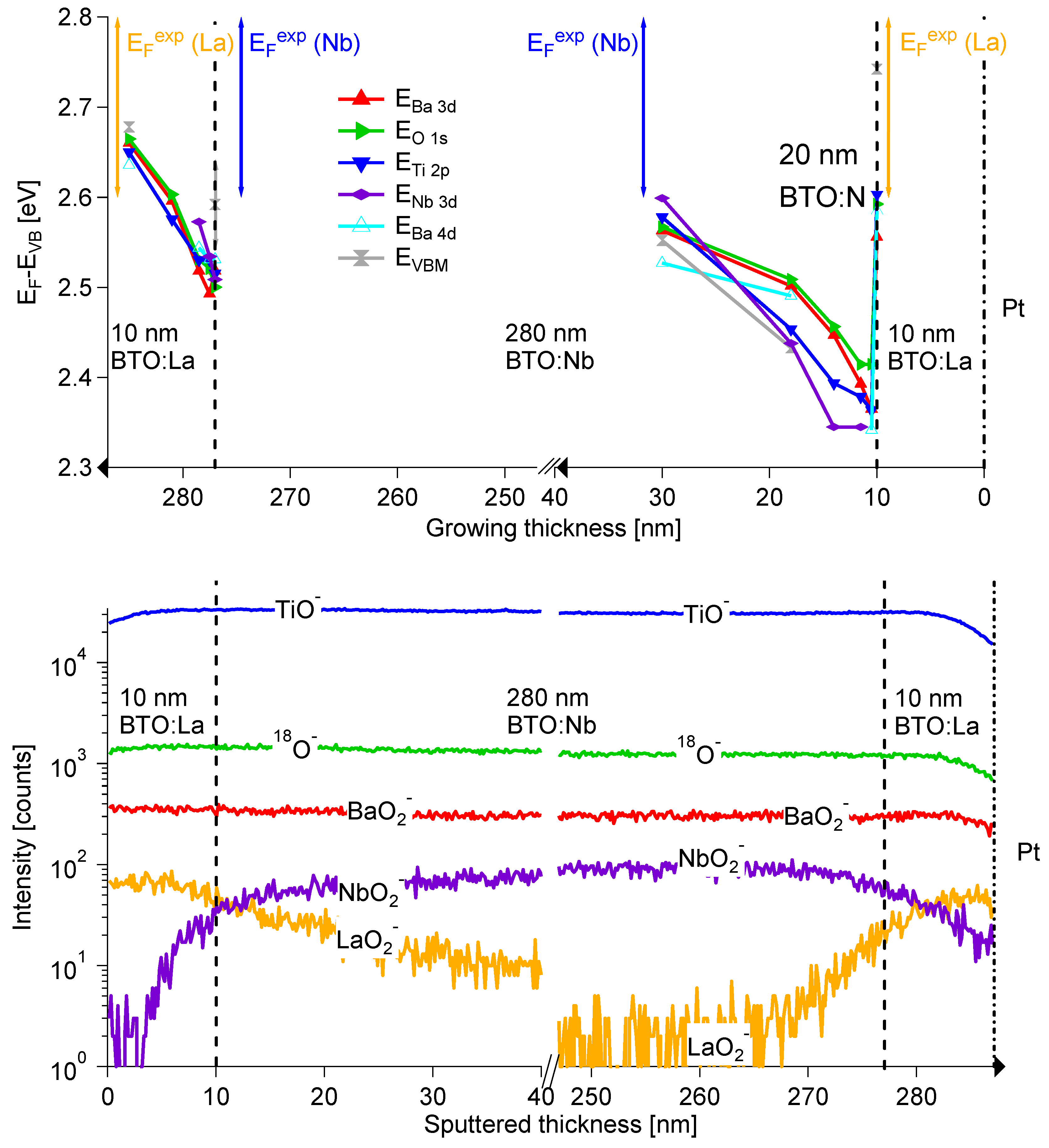
To confirm an interfacial contribution to the dielectric properties of the LNL heterostructure, we investigated the electronic structure of the interface between La-doped and Nb-doped BaTiO3 films by in situ XPS [26]. The evolution of the Fermi level with respect to the valence band maximum (EF-EVB) was followed during a step-by-step deposition of either an La-doped on an Nb-doped layer (Figure 7, top left) or vice versa (Figure 7, top right). After each deposition step, the value EF-EVB was obtained by measuring both the leading edge of the valence band maximum and the core level binding energy of any BaTiO3 core level (Ba 3d5/2, O 1s, Ti 2p) (Kraut method) [27]. The experiment was conducted in several steps: (i) a 10-nm-thick La-doped layer was deposited onto the Si/Pt substrate; (ii) for studying the deposition induced changes, a stepwise deposition of an Nb-doped layer was performed until a thickness of 20 nm was reached; (iii) an Nb-doped layer of 260 nm was deposited to complete the total thickness of the Nb-doped layer of 280 nm; (iv) an La-doped layer was stepwise deposited until a thickness of 10 nm to follow the effect on the interface. The sequence of the experiment is shown in Figure 7 at the top from right to left.
A sharp immediate drop in Fermi level (0.25 eV) and a consecutive variation of band position over about 20 nm was observed during deposition of the Nb-doped layer onto La-doped substrate (right), whereas less pronounced effects (0.1 eV, 8 nm) were observed for the reverse deposition (left). The sharp drop in Fermi level after the initial deposition of Nb-doped BTO onto the La-doped substrate was not expected, as donor type dopants were present in both films. However, it was observed that the abrupt lowering of EF is associated with an unexpectedly high Nb intensity in the XPS spectra, which suggests an enhanced Nb concentration at this interface. This might be the origin for the depletion layer and the enhanced permittivity. Nb is a donor in BTO and lightly doped polycrystalline bulk ceramics show resistivities of 10 Ωcm and a pronounced positive temperature coefficient of resistivity (PTCR) [7,28,29]. When the Nb concentration is increased above 0.1 wt%, the samples become insulating again. This behavior is likely related to insulating grain boundaries, which are probably induced by segregation of Ba vacancies or Nb donors to the grain boundary core. It is not expected that the grains themselves become insulating with an increasing donor concentration.
TOF-SIMS is a very efficient way to qualitatively assess the presence of dopants in individual layers as well as their interdiffusion at interfaces in multilayers. Using TOF-SIMS, we could confirm that the three types of dopants were indeed present in every individual layers and that the Nb concentration is enhanced near the bottom interface. In order to obtain further insight into interface chemistry, TOF-SIMS depth profiling experiments were performed on the LNL10 heterostructure using 1 keV Cs+ for sputtering and 30 keV Bi+ for analysis. Whereas XPS experiments were performed during the growth, TOF-SIMS was performed ex situ on the same sample in reverse order by depth profiling. The evolution of intensities with sputter time is given from left to right in Figure 7.
Starting from the top of the heterostructure, the interface from the La-doped layer towards the Nb-doped one is as sharp as expected from the depth resolution of TOF-SIMS [30]. Meanwhile, the Nb signal is very small in the La-doped layer, which shows that interdiffusion of dopants did not occur. This is slightly different for the bottom interface close to the Si/Pt substrate. The intensity of the Gaussian-like LaO2- peak remains below that of the outer La-doped layer, whereas the intensity of the NbO2- peak does not decay as fast as expected without interdiffusion (=Imax/3 in the middle of the layer). Long range interdiffusion between the dopant ions was thus much more efficient at the bottom Nb/La interface as compared to the top La/Nb one. In agreement with the XPS analysis, the Nb content near the bottom interface was also larger than at the top contact.
Such interface contrast between bottom and top interfaces has been observed by in-situ XPS in metal/ferroelectric/metal structures and explained in terms of a different thermal budget [31]. The bottom interface was exposed to the growth temperature of 650 °C for several hours, while the top interface was only exposed for a few minutes. We therefore ascribed the strong disparity in the La/Nb/La heterostructures to the thermal history of the sample. What is new here, and obviously not observed in metal/ferroelectric interfaces, is that cross diffusion of dopants through oxide/oxide interfaces is possible because of the crystalline continuity at the interface and column-like grains. This is why we linked the specific band bending at the bottom Nb/La interface observed by in-situ XPS to the interdiffusion observed by TOF-SIMS.
For all other investigated interfaces, the band bending was much smoother and the interdiffusion between layers much more limited, leading to a moderate increase in dielectric permittivity in NLN and NMN cases.
4. Conclusions
To summarize, we have achieved large and temperature-stable dielectric permittivity by a three-layer stack of La-doped and Nb-doped BaTiO3 thin films. Using XPS, we could link these features to interface localization of space charges resulting in large band bending over more than a thickness of 10 nm (see Figure 7). TOF-SIMS experiments suggest that this band bending results from cross diffusion of dopants at the interface. Such layered structures may be useful to model so-called giant permittivity in isotropic polycrystalline samples.
Author Contributions
Conceptualization, C.C.C., M.M., A.K. and S.P.; validation, C.C.C.; formal analysis, C.C.C.; investigation, C.C.C., M.M., A.K. and S.P.; resources, M.M., Andreas Klein and J.-P.S.; data curation, M.M. and A.K.; writing—original draft preparation, C.C.C. and M.M.; writing—review and editing, M.M., A.K. and J.-P.S.; visualization, C.C.C.; supervision, M.M. and A.K.; project administration, C.C.C.; funding acquisition, M.M., A.K. and S.P. All authors have read and agreed to the published version of the manuscript.
Funding
This research received the funding from the French-German School and Horizon 2020 Framework Programme: 641640.
Acknowledgments
We also acknowledge support by the German Research Foundation and the Open Access Publishing Fund of Technical University of Darmstadt.
Conflicts of Interest
The authors declare no conflict of interest.
References
- Sigman, J.; Brennecka, G.L.; Clem, P.G.; Tuttle, B.A. Fabrication of perovskite-based high-value integrated capacitors by chemical solution deposition. J. Am. Ceram. Soc. 2008, 91, 1851–1857. [Google Scholar] [CrossRef]
- Dietz, G.W.; Schumacher, M.; Waser, R. Leakage currents in Ba 0.7 Sr 0.3 TiO3 thin films for ultrahigh-density dynamic random access memories dynamic random access memories. J. Appl. Phys. 2014, 82, 2359. [Google Scholar] [CrossRef]
- Lemée, N.; Dubourdieu, C.; Delabouglise, G.; Sénateur, J.P.; Laroudie, F. Semiconductive Nb-doped BaTiO3 films grown by pulsed injection metalorganic chemical vapor deposition. J. Cryst. Growth 2002, 235, 347–351. [Google Scholar] [CrossRef]
- Dubourdieu, C.; Bruley, J.; Arruda, T.M.; Posadas, A.; Jordan-Sweet, J.; Frank, M.M.; Cartier, E.; Frank, D.J.; Kalinin, S.V.; Demkov, A.A.; et al. Switching of ferroelectric polarization in epitaxial BaTiO 3 films on silicon without a conducting bottom electrode. Nat. Nanotechnol. 2013, 8, 748–754. [Google Scholar] [CrossRef]
- Tabata, H.; Tanaka, H.; Kawai, T. Formation of artificial BaTiO3/SrTiO3 superlattices using pulsed laser deposition and their dielectric properties. Appl. Phys. Lett. 2006, 1970, 1998–2001. [Google Scholar]
- Horwitz, J.S.; Chang, W.; Kim, W.; Qadri, S.B.; Pond, J.M.; Kirchoefer, S.W.; Chrisey, D.B. The effect of stress on the microwave dielectric properties of BaO5 SrO5 TiO3 thin films. J. Electron. 2000, 3, 357–363. [Google Scholar]
- Heywang, W. Semiconducting barium titanate. J. Mater. Sci. 1971, 6, 1214–1224. [Google Scholar] [CrossRef]
- Ramirez, A.P.; Subramanian, M.A.; Gardel, M.; Blumberg, G.; Li, D.; Vogt, T.; Shapiro, S.M. Giant dielectric constant response in a copper-titanate. Solid State Commun. 2000, 115, 217–220. [Google Scholar] [CrossRef]
- Ikeda, N.; Ohsumi, H.; Ohwada, K.; Ishii, K.; Inami, T.; Kakurai, K.; Murakami, Y.; Yoshii, K.; Mori, S.; Horibe, Y.; et al. Ferroelectricity from iron valence ordering in the charge-frustrated system LuFe2O4. Nature 2005, 436, 1136–1138. [Google Scholar] [CrossRef]
- Wu, J.; Nan, C.W.; Lin, Y.; Deng, Y. Giant dielectric permittivity observed in Li and Ti doped NiO. Phys. Rev. Lett. 2002, 89, 1–4. [Google Scholar] [CrossRef]
- Popovic, Z.V.; Stolz, H.J. Infrared and raman spectra of germanium dichalcogenides I. GeS2. Phys. Stat. Solid. B 1981, 106, 337–348. [Google Scholar] [CrossRef]
- Arveux, E.; Payan, S.; Maglione, M.; Klein, A. Applied Surface Science Surface segregation in Nb-doped BaTiO3 films. Appl. Surf. Sci. 2010, 256, 6228–6232. [Google Scholar] [CrossRef]
- Reymond, V. Nouvelles Couches Minces et Multicouches Dérivées de Batio3: Optimisation des Propriétés Diélectriques. Ph.D. Thesis, Université de Bordeaux, Bordeaux, France, 2004. [Google Scholar]
- Simon, Q.; Daumont, C.J.M.; Payan, S.; Gardes, P.; Poveda, P.; Wolfman, J.; Maglione, M. Extreme dielectric non-linearities at the convergence point in Ba1-xCaxTi1-xZrxO3 thin films. J. Alloys Compd. 2018, 747, 366–373. [Google Scholar] [CrossRef]
- Klein, A. Interface properties of dielectric oxides. J. Am. Ceram. Soc. 2016, 99, 369–387. [Google Scholar] [CrossRef]
- Levasseur, D. Nouvelle Génération de Capacités Intégrées: Influence des Matériaux sur les Performances Diélectriques des Capacités en Couches Minces. Ph.D. Thesis, Université de Bordeaux, Bordeaux, France, 2015. [Google Scholar]
- Arveux, E. Propriétés de Surfaces et Interfaces de Couches Minces Ferroélectriques de BaTiO3 Étudiées par Spectroscopie de Photoémission in-situ. Ph.D. Thesis, Université de Bordeaux, Bordeaux, France, 2009. [Google Scholar]
- Maglione, M.; Belkaoumi, M. Electron-relaxation-mode interaction in Ba Ti03: Nb. Phys. Rev. B 1992, 45, 2029–2034. [Google Scholar] [CrossRef]
- Reymond, V.; Payan, S.; Michau, D.; Manaud, J.; Maglione, M. Structural and electrical properties of BaTi1 à x Zr xO3 sputtered thin films: Effect of the sputtering conditions. Thin Solid Films 2004, 467, 54–58. [Google Scholar] [CrossRef]
- van Benthem, K.; Elsässer, C.; French, R.H. Bulk electronic structure of experiment and theory. J. Appl. Phys. 2011, 90, 6156. [Google Scholar] [CrossRef] [Green Version]
- Chan, H.M.; Harmer, M.P.; Smyth, D.M. Compensating defects in highly donor-doped BaTiO3. J. Am. Ceram. Soc. 1986, 10, 507–510. [Google Scholar] [CrossRef]
- Morrison, F.D.; Coats, A.M.; Sinclair, D.C.; West, A.R. Charge compensation mechanisms in La-doped BaTiO3. J. Electroceramics 2001, 6, 219–232. [Google Scholar] [CrossRef]
- Chambers, S.A.; Droubay, T.; Kaspar, T.C.; Gutowski, M.; Van Schilfgaarde, M. Accurate valence band maximum determination for SrTiO3(0 0 1). Surf. Sci. 2004, 554, 81–89. [Google Scholar] [CrossRef]
- Moretti, P.; Michel-Calendini, F.M. Impurity energy levels and stability of CR and MN ions in cubic batio3. Phys. Rev. B 1987, 36, 3522–3527. [Google Scholar] [CrossRef] [PubMed]
- Wechsler, B.A.; Klein, M.B. Thermodynamic point defect model of barium titanate and application to the photorefractive effect. J. Opt. Soc. Am. B 1988, 5, 1711. [Google Scholar] [CrossRef]
- Klein, A. Energy band alignment at interfaces of semiconducting oxides: A review of experimental determination using photoelectron spectroscopy and comparison with theoretical predictions by the electron affinity rule, charge neutrality levels, and the common anion. Thin Solid Films 2012, 520, 3721–3728. [Google Scholar] [CrossRef]
- Kraut, E.A.; Grant, R.W.; Waldrop, J.R.; Kowalski, S.P. Precise determination of the Valence-Band Edge in X-ray Photoemission spectra: Application to measurement of semiconductor interface potentials. Phys. Rev. Lett. 1980, 44, 1620–1623. [Google Scholar] [CrossRef]
- Slipenyuk, A.M.; Glinchuk, M.D.; Laguta, V.V.; Bykov, I.P.; Bilous, A.G.; V’yunov, O.I. Impurity and intrinsic defects in barium titanate ceramics and their influence on PTCR effect. Ferroelectrics 2003, 288, 243–251. [Google Scholar] [CrossRef]
- Lewis, G.V.; Catlow, C.R.A. PTCR Effect in BaTiO3. J. Am. Ceram. Soc. 1985, 58, 555–558. [Google Scholar] [CrossRef]
- Hofmann, S.; Liu, Y.; Jian, W.; Kang, H.L.; Wang, J.Y. Depth resolution in sputter profiling revisited. Surf. Interface Anal. 2016, 48, 1354–1369. [Google Scholar] [CrossRef]
- Schafranek, R.; Payan, S.; Maglione, M.; Klein, A. Barrier height at (Ba, Sr) TiO3/Pt interfaces studied by photoemission. Phys. Rev. B 2008, 30–33. [Google Scholar] [CrossRef]
Figure 1.
Multilayer structures with Pt top electrodes for electric measurements. Left: LNL10. Right: MNM20.
Figure 1.
Multilayer structures with Pt top electrodes for electric measurements. Left: LNL10. Right: MNM20.

Figure 2.
XRD diffraction patterns (2 theta) of (un)doped samples.

Figure 3.
Temperature dependence of the relative permittivity and dielectric losses at 100 kHz of Nb- and La-doped BaTiO3 films and of an LNL10 multilayer structure.
Figure 3.
Temperature dependence of the relative permittivity and dielectric losses at 100 kHz of Nb- and La-doped BaTiO3 films and of an LNL10 multilayer structure.

Figure 4.
Dielectric permittivity and dielectric losses vs. frequency (Vosc = 0.01 V) of (un)doped samples and different multilayer heterostructures at 293 K.
Figure 4.
Dielectric permittivity and dielectric losses vs. frequency (Vosc = 0.01 V) of (un)doped samples and different multilayer heterostructures at 293 K.

Figure 5.
XPS survey (top) and core-levels and valence bands (VB) (bottom) of an undoped BaTiO3 thin film recorded with monochromatized Al Kα radiation.
Figure 5.
XPS survey (top) and core-levels and valence bands (VB) (bottom) of an undoped BaTiO3 thin film recorded with monochromatized Al Kα radiation.

Figure 6.
Fermi level position of differently doped BaTiO3 thin samples analyzed directly after deposition without breaking vacuum (in-situ) or after deposition in a disconnected deposition chamber after surface cleaning by annealing in a low-pressure oxygen environment (ex-situ).
Figure 6.
Fermi level position of differently doped BaTiO3 thin samples analyzed directly after deposition without breaking vacuum (in-situ) or after deposition in a disconnected deposition chamber after surface cleaning by annealing in a low-pressure oxygen environment (ex-situ).

Figure 7.
Top. In situ XPS stepwise interface experiments of 8 nm thick BTO:La layer on a BTO:Nb layer (left) and a 20-nm-thick BTO:Nb layer on a BTO:La substrate (right). First points (starting from dashed lines) correspond to a single doped layer. For reference, the range of Fermi level positions with respect to the valence band of single doped films obtained by XPS in situ is plotted. As ECL-EVBM is a material constant, the values of core level positions of each element were obtained by subtracting: 776.57 eV for Ba3d, 527.09 eV for O1s, 455.79 eV for Ti2p, 204.40 eV for Nb3d and 86.07 eV for Ba4d (values obtained by averaging over 100 samples). Error on these values is ±0.05 eV. Bottom. Time-of-flight secondary ion mass spectroscopy (TOF-SIMS) depth profiling of sample LNL10. Analyzed ion species are written over their corresponding lines.

Figure 8.
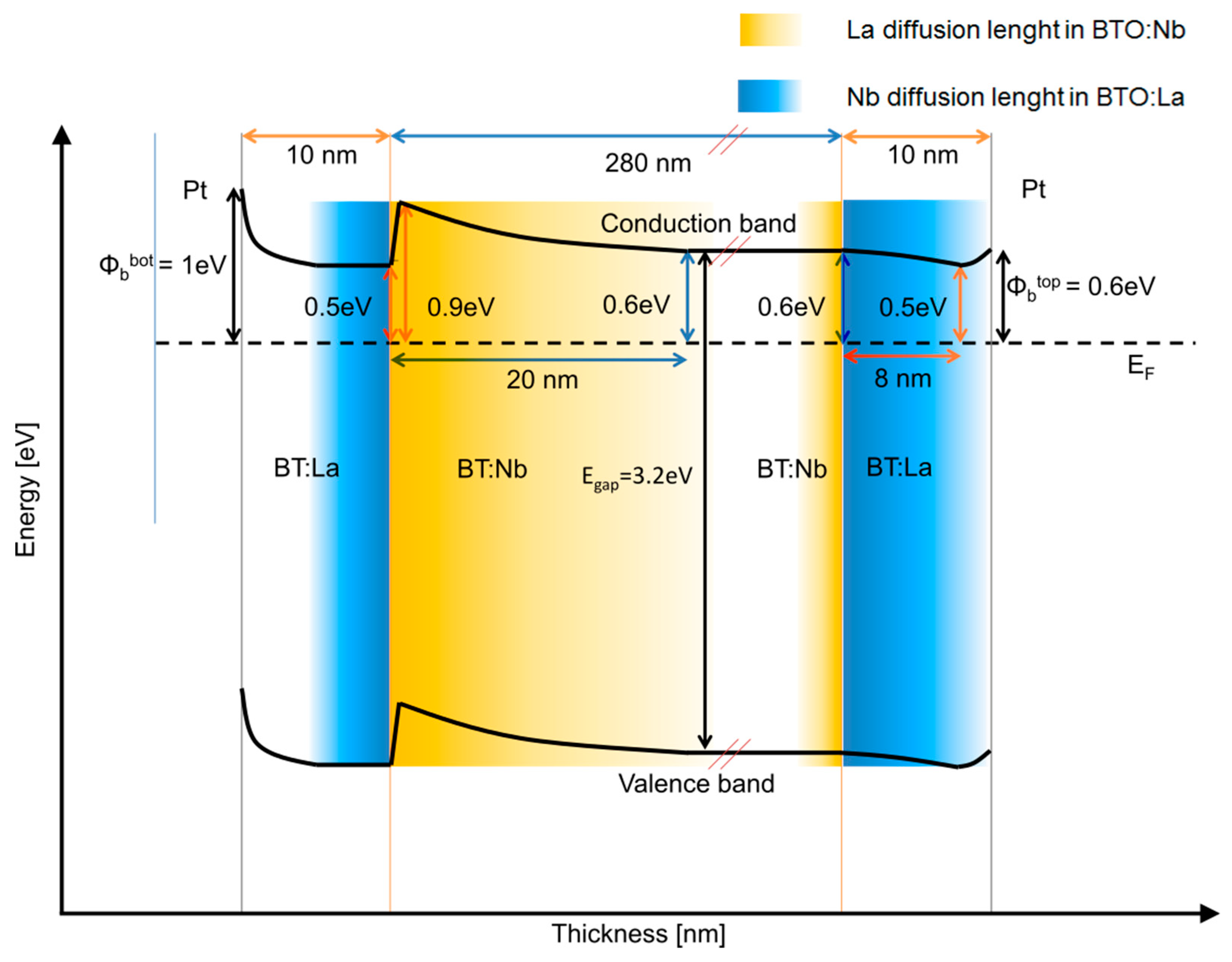
Band diagram of capacitor LNL10 with Pt barrier heights derived from the results of E. Arveux [17].
Figure 8.
Band diagram of capacitor LNL10 with Pt barrier heights derived from the results of E. Arveux [17].


Table 1.
Physical vapor deposition (PVD) sputtering conditions for (un) doped BaTiO3 (BTO) thin films and doping concentration of targets.
Table 1.
Physical vapor deposition (PVD) sputtering conditions for (un) doped BaTiO3 (BTO) thin films and doping concentration of targets.
| Sputtering Conditions | |
| Power density (W/cm2) | 2.5 |
| Pressure (Pa) | 5 |
| Ar/O2 gas content (sccm) | 99/1 (1% O2) |
| Temperature (°C) | 650 |
| Substrate distance (cm) | 8 |
| Deposition rate (nm/min) | 2.5 |
| Targets Composition | |
| BaTiO3 | Nominally undoped |
| BaTiO3:Mn | 0.23 wt% (0.10 at%) |
| BaTiO3:Nb | 0.05 wt% (0.12 at%) |
| BaTiO3:La | 0.50 wt% (0.83 at%) |
Table 2.
Relative permittivity and dielectric losses values are shown for 100 kHz, 0 V and room temperature. XPS results are in situ EF (Fermi level position) —EVBM (valence band maximum) (eV) values for single doped films and ex situ EF-EVBM values for heterostructures. The abbreviations indicate tri-layer structures where M, N, and L correspond to Mn, Nb and La, respectively.
| Single Doped Films | |||
| Sample | ε | tan (δ) (%) | XPS (eV) |
| Undoped | 110 | 1.5 | 2.7 |
| Mn doped | 250 | 1.1 | 2.2 |
| La doped | 400 | 2.2 | 2.8 |
| Nb doped | 640 | 2.0 | 2.8 |
| Heterostructures | |||
| Sample | ε | tan (δ) (%) | XPS (eV) |
| MNM20 | 400 | 1.3 | 2.2 |
| MNM10 | 530 | 2.2 | 2.2 |
| MNM5 | 850 | 5.0 | 2.4 |
| NMN20 | 440 | 2.5 | 2.1 |
| LNL10 | 1100 | 3.1 | 2.3 |
| NLN10 | 540 | 2.3 | 2.3 |
© 2020 by the authors. Licensee MDPI, Basel, Switzerland. This article is an open access article distributed under the terms and conditions of the Creative Commons Attribution (CC BY) license (http://creativecommons.org/licenses/by/4.0/).
Share and Cite
MDPI and ACS Style
Chavarría, C.C.; Payan, S.; Salvetat, J.-P.; Maglione, M.; Klein, A. Fermi Level Engineering for Large Permittivity in BaTiO3-Based Multilayers. Surfaces 2020, 3, 567-578. https://0-doi-org.brum.beds.ac.uk/10.3390/surfaces3040038
AMA Style
Chavarría CC, Payan S, Salvetat J-P, Maglione M, Klein A. Fermi Level Engineering for Large Permittivity in BaTiO3-Based Multilayers. Surfaces. 2020; 3(4):567-578. https://0-doi-org.brum.beds.ac.uk/10.3390/surfaces3040038
Chicago/Turabian StyleChavarría, Christopher Castro, Sandrine Payan, Jean-Paul Salvetat, Mario Maglione, and Andreas Klein. 2020. "Fermi Level Engineering for Large Permittivity in BaTiO3-Based Multilayers" Surfaces 3, no. 4: 567-578. https://0-doi-org.brum.beds.ac.uk/10.3390/surfaces3040038