Article

Synthesis of MoS2 Thin Film by Ionized Jet Deposition: Role of Substrate and Working Parameters

1
Department of Chemistry, Life Science and Environmental Sustainability—University of Parma, Parco Area delle Scienze 17/A, 43124 Parma, Italy
2
IMEM-CNR Institute of Materials for Electronics and Magnetism, Trento unit c/o Fondazione Bruno Kessler, Via alla Cascata 56/C, Povo, 38123 Trento, Italy
3
CNR-IFN, CSMFO Lab & FBK Photonics Unit, Via Alla Cascata 56/C, Povo, 38123 Trento, Italy
*
Author to whom correspondence should be addressed.
Submission received: 27 November 2020 / Revised: 10 December 2020 / Accepted: 11 December 2020 / Published: 13 December 2020
(This article belongs to the Special Issue Thin Films at Surfaces)

Abstract

:
The lack of scalable synthesis of transition metal dichalcogenides, such as molybdenum disulfide (MoS2), has proved to be a significant bottleneck in realization of fundamental devices and has hindered the commercialization of these materials in technologically relevant applications. In this study, a cost-efficient and versatile thin-film fabrication technique based on ionized jet deposition (IJD), i.e., a technique potentially providing high processing efficiency and scalability, is used to grow MoS2 thin films on silicon substrates. The operating conditions of IJD were found to influence mainly the ablation efficiency of the target and only slightly the quality of the deposited MoS2 thin film. All as-deposited films show chemical properties typical of MoS2 with an excess of free, elemental sulfur that can be removed by post-deposition annealing at 300–400 °C, which also promotes MoS2 crystallization. The formation of an interface comprised of several silicon oxide species was observed between MoS2 and the silicon substrate, which is suggested to originate from etching and oxidizing processes of dissociated water molecules in the vacuum chamber during growth. The present study paves the way to further design and improve the IJD approach for TMDC-based devices and other relevant technological applications.

1. Introduction

Two-dimensional transition metal dichalcogenides (TMDCs) such as MoS2, WS2, MoSe2, and NbSe2 have recently attracted enormous technological and scientific interest due to their remarkable mechanical, electronic, and optical properties that greatly differ from their bulk counterparts [1,2,3]. For instance, owing to their tunable band gap by simply varying the number of layers, laboratory-scale TMDC-based electronic devices such as transistors [4,5], sensors [6,7], memristors [8,9], etc. have been demonstrated using few or single-layer materials, and the outcome sparked hopes to obtain highly efficient electronic devices beyond silicon-based technology. However, the realization of electronic devices based on TMDCs suffers from yet unsolved challenges, such as controlling their surface electronic properties, understanding the role of defects and/or scalable synthesis of few/single layer TMDCs with large dimensions and good mechanical stability. Various synthesis routes have been developed to grow MoS2 as the most prominent TMDC material, including exfoliation methods [10,11,12], chemical vapor deposition (CVD) [13], wet-chemistry approaches [14,15], pulsed laser deposition (PLD) [16], and magnetron sputtering [17]. However, most of these techniques still lack industrial scalability for simple and low-cost production of MoS2 with uniform and reproducible material properties.
In this work, MoS2 thin films were grown on native oxide-covered silicon substrates (SiO2/Si) using a novel up-scalable pulsed electron deposition technique; namely, ionized jet deposition (IJD) [18,19,20]. The IJD growth is based on an ionized gas jet that acts as source/carrier gas for highly energetic electrons, and, in a second step, as plasma for the ablated material. To promote MoS2 crystallization, we used a two-step approach consisting of IJD thin film growth and post-deposition annealing in ultra-high vacuum (UHV). Since the efficiency of material ablation and the quality of the final product depends on various growth parameters, such as IJD discharge acceleration voltage and deposition frequency, we systematically varied the IJD operating parameters, and applied different annealing temperatures of up to 400 °C. The as-deposited and annealed samples were investigated via X-ray photoelectron spectroscopy (XPS) to identify optimized growth and annealing conditions. Furthermore, the interaction of the oxide-containing substrate (SiO2/Si) with the IJD plasma was investigated by XPS. In particular, the formation of a complex silicon oxide interface was observed, whose origin is ascribed to reactions with residual water due to the relatively high base pressure in the deposition chamber (5 × 10⁻⁶ mbar).
To obtain a comprehensive understanding of the chemical, vibrational, and structural properties of the IJD-derived MoS2 thin films, a variety of other characterization techniques have been used such as Raman spectroscopy and XRD to evaluate crystallinity, as well as SEM and AFM for characterization of the surface morphology.

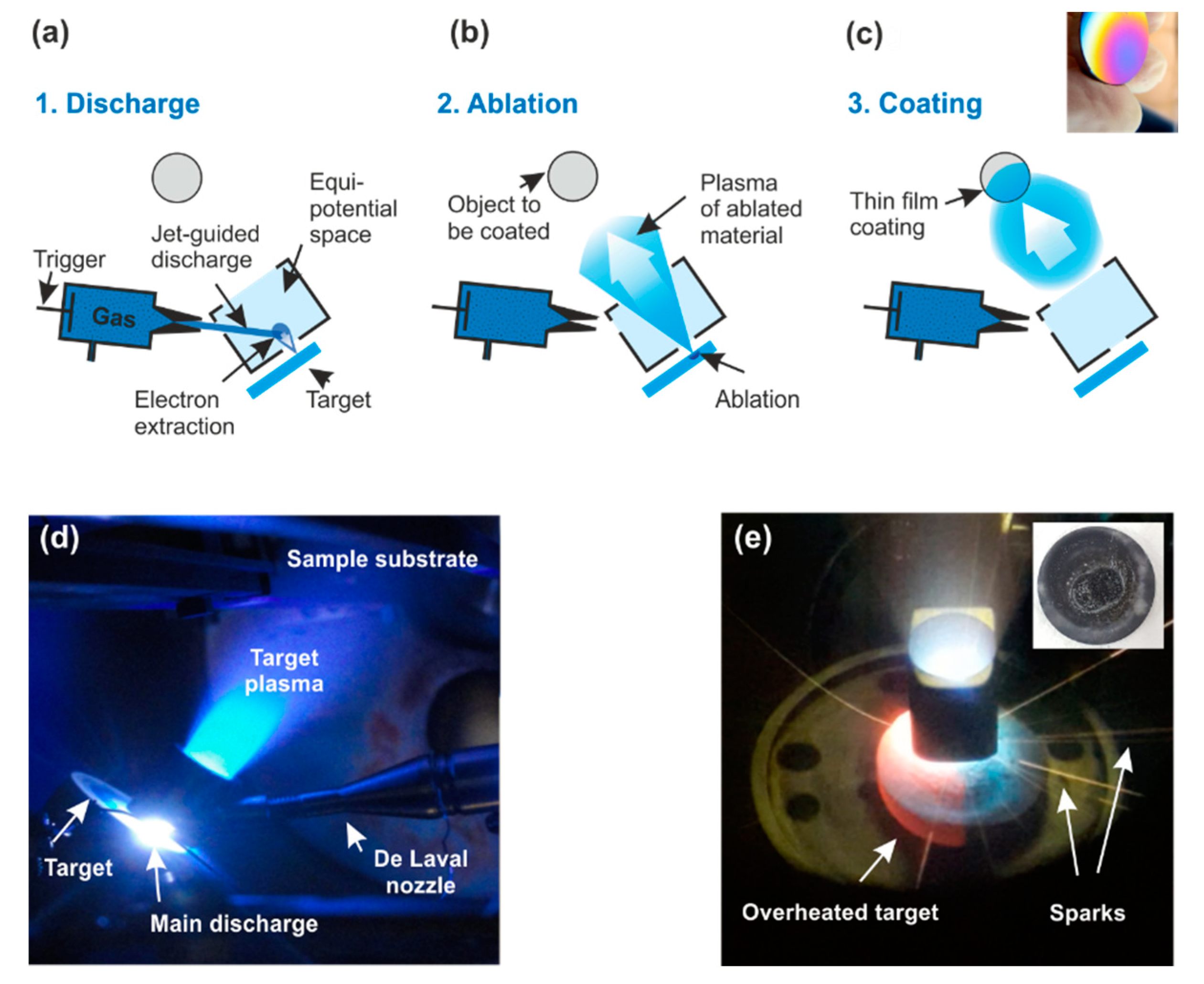
2. Materials and Methods
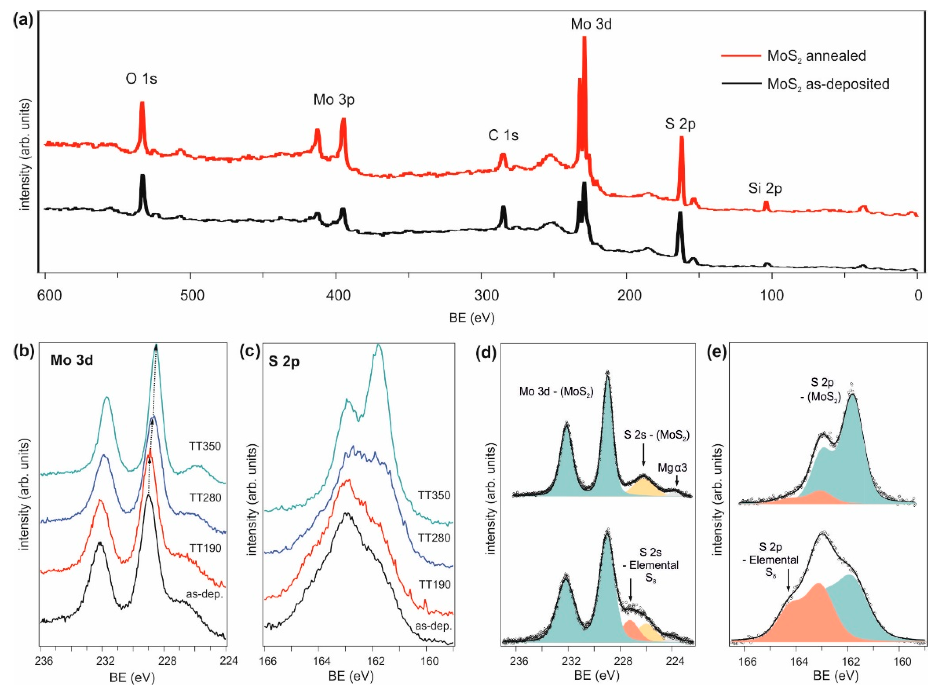
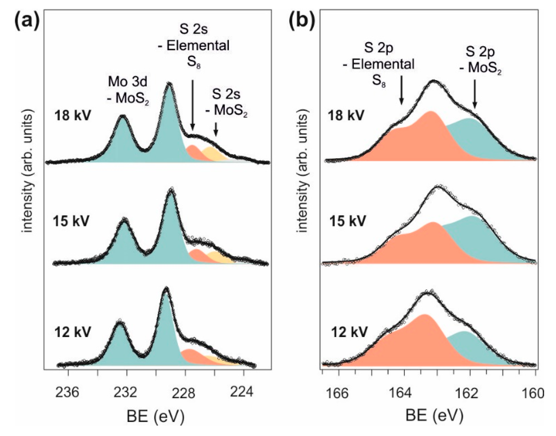
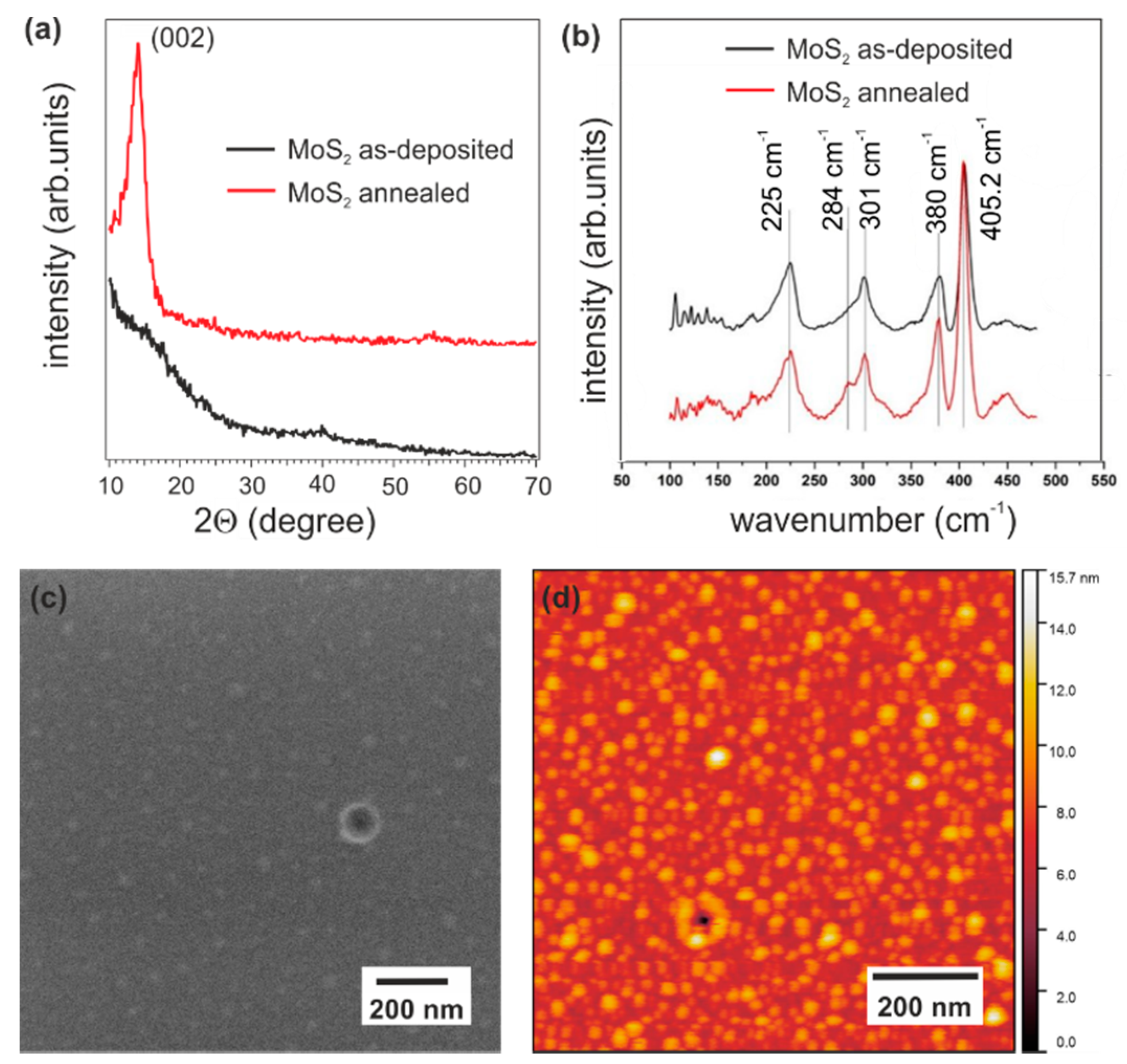
Figure 1a–c schematically illustrates the main components and principles of the IJD source [18,19,20] for MoS2 thin film growth. An ionized working gas such as Ar+ passes through a convergent-divergent De Laval nozzle [21] that creates an ultrafast supersonic gas flow in its widening part. This ionized gas jet enters a cylinder-shaped hollow cathode, in which the electrons of the ionized gas multiply and become electrostatically confined in an equipotential space. The fast oscillation of electrons within the hollow cathode leads to a cascade ionization of the working gas, ultimately increasing the overall ionization density by orders of magnitude, which is known as a hollow-cathode effect [22]. Due to the jet-guided discharge (see Figure 1a), high-density electrons are directed towards the grounded MoS2 target. The highly energetic pulsed electron beam ablates the MoS2 target and produces a plasma plume of ejected molecular-sized Mox−Sy species that propagate with the working gas through the hollow cathode towards the substrate (see Figure 1b). Finally, the Mox−Sy species from the target condense as nm-sized clusters on the substrate, forming a MoS2 thin film over a large area (see Figure 1c), i.e., coating 5-inch wafers or larger. The geometry inside the IJD chamber with the formation of the main discharge and target plasma during MoS2 thin film growth is depicted in Figure 1b.
In the present study, the target material was a commercial MoS2 cylindrical target (Testbourne Ltd., Ø = 5 cm, thickness = 0.5 cm) of 99.95% purity. A substrate for thin film growth, Si (001) with its native oxide layer was used. The distance between gun hat (smaller bottom opening of the hollow cylinder) and the target was set to about 1 cm, while the substrate was positioned about 12–13 cm from the top of the hollow cylinder, resulting in a target-to-substrate distance of ~15 cm. To improve material consumption and film uniformity, both target and substrate kept rotating in opposite directions during the deposition process. The base pressure in the lab-grade IJD chamber was 5 × 10⁻⁶ mbar, which increased up to 4 × 10⁻³ mbar using Ar as working gas and plasma formation. All samples were grown with the substrate at room temperature. As first IJD process parameter, we optimized the discharge frequency, which is usually f ≤ 300 Hz (pulse length 100–300 ns). It was found that deposition frequencies above 250 Hz often increased the temperature on the MoS2 target material, as evidenced by a dark red color visible on the target and formation of sparks during deposition (see Figure 1e). In a second step, we evaluated the range of electron acceleration voltages (V = 10–30 kV). It was found that acceleration voltages lower than 12 kV were not able to induce a reliable ablation process (i.e., the plasma was not stable and frequently turned on and off), whereas V > 18 kV led to an irregular plasma arising during IJD deposition, with the target reaching high temperatures as again evidenced by a dark red color and formation of craters on the surface of the target (see Figure 1e).
Therefore, the IJD discharge parameters were set with a constant frequency of f = 150 Hz using three different acceleration voltages V = 12, 15 and 18 kV and different deposition times between 20 and 60 min. The as-deposited thin films were annealed in ultra-high vacuum (UHV, p = 2 × 10⁻¹⁰ mbar) at different temperatures T = 190–400 °C for 60 min. A freshly exfoliated MoS2 single crystal was used as reference material during the experiment.
XPS analyses were performed with a non-monochromatized Mg Kα X-ray source (emission line at 1253.6 eV) and a helium discharge lamp (emission line at 21.21 eV). The total resolution was 0.8 eV for XPS analysis. The binding energy (BE) scale of XPS spectra was calibrated by using the Au 4f peak at 84.0 eV as reference Core level analyses were performed by Voigt line-shape deconvolution after background subtraction of a Shirley function.
XRD spectra were collected on films with a Rigaku D/max III diffractometer in glancing incident configuration, using Cu Kα radiation and a graphite monochromator in the diffracted beam. Asymmetric scan geometry was adopted to enhance the signal stemming from the IJD-MoS2 thin film. The typical measurements were performed in the 2ϴ range of 10–70° with an incidence angle of 1°, sampling interval of 0.05°, and counting time of 8 s.
Non-resonant Raman and PL spectra were acquired at room temperature using a LabRAM Aramis (Horiba Jobin-Yvon, Palaiseau, France), equipped with diode-pumped solid-state laser lines of 532 and 632 nm. The laser line was focused on the sample by a 100× objective lens. The luminescence and the Raman spectra were detected with an air-cooled charge-coupled detector (CCD). The collected light was dispersed by a 1800 grooves/mm spectrometer. In Raman spectra acquisition, the Rayleigh line below 100 cm−1 was filtered and the silicon Raman band, which is located at 520 cm−1, was used as reference. The resolution of the obtained spectra was 1 cm−1.
The morphology of the samples was analyzed via scanning electron microscopy (SEM) in a field-emission Supra 40/40VP Zeiss SEM using secondary electrons for imaging. The atomic force microscopy (AFM) images were acquired using a SFC100SEMI Universal SPM scanning Head 1, acquiring the images on a 1.5 × 1.5 μm2 area.

3. Results

3.1. Influence of Annealing Temperature

We performed different post-deposition thermal treatments (T = 190–350 °C) of the sample deposited at 15 kV acceleration voltage for 60 min. Chemical analysis of the as-deposited sample as well as after each annealing step was conducted by in-situ XPS to investigate the composition/stoichiometry of the thin films and the influence of annealing temperature, as shown in Figure 2. The XPS wide range spectra of as-deposited and annealed thin film are reported in Figure 2a and confirm the presence of molybdenum (Mo) and sulfur (S), as well as silicon (Si) and SiO2 (due to the substrate) with its oxygen counterpart, and carbon related to contaminations during the growth process and/or after air exposure.
The Mo 3d5/2 peak of the as-deposited thin film (see Figure 2b) is located at a binding energy (BE) of ~229 eV, and the S 2s core level appears as broad shoulder at around 226 eV. With increasing annealing temperature, the Mo 3d spectral features are shifted to lower BEs, and the line shape of the S 2s peak slightly changes, indicating a decrease of the intensity contribution at around 227 eV. Figure 2c shows the corresponding S 2p core level region of the as-deposited sample and its evolution with increasing temperature. In the as-deposited case, the S 2p core level region appears as broad unresolved feature with a small shoulder at the high BE side. The S 2p3/2 core level is located at around 162 eV. With increasing annealing temperature, the S 2p features are shifted to lower BEs, in agreement with the observed shift in Figure 1b. Moreover, the line shape drastically changes and reaches the typical S 2p line shape of MoS2 after annealing at T = 350 °C. Furthermore, the high BE side shoulder gradually decreases with increasing temperature, suggesting the loss of a minor sulfur component leading to a more chemical uniformity of the sample.
The deconvolved Mo 3d and S 2p spectra of as-deposited thin film and the one annealed at the highest temperature (T = 350 °C) are shown in Figure 2d,e. A summary of the BE positions of the fitted components, as well as their full width at half maximum (FWHM) and estimated stoichiometric compositions (S/Mo ratio) is given in Table 1. In both samples, the main Mo 3d component in Figure 2d originates from Mo4+ species of MoS2 (gray-blue component), with a slightly narrower line shape in the annealed sample. The S 2s core level region of the as-deposited sample exhibits two components (yellow and red in Figure 2d), which contrasts with the annealed sample, where only one S 2s component (yellow) is present. Similar to the spectrum in Figure 2d, the S 2p core level of the as-deposited sample in Figure 2e exhibits an additional S 2p peak (red component), suggesting that some sulfur atoms exhibit a different chemical environment (other than Mo−S) in the as-deposited thin film. This additional component can be attributed to unbound elemental sulfur that is greatly decreased after annealing at T = 350 °C. Hence, the high BE side shoulder observed in Figure 2c can be attributed to unbound elemental sulfur that can be gradually removed with increasing temperature, which is also evidenced by the reduced S/Mo ratio (considering both sulfur components, see Table 1). With increasing temperature, the S/Mo ratio approaches the expected stoichiometric value of MoS2, suggesting a loss of elemental sulfur due to annealing. It should be noted that, by excluding the additional S species, the S/Mo ratio in the as-deposited thin film is already close to 2, i.e., the expected value of MoS2, indicating the deposition of stoichiometric MoS2 even without annealing and despite the presence of elemental sulfur.

3.2. Influence of Acceleration Voltage

To better identify the role of the energy of the pulsed electrons in the IJD deposition process, we investigated another two acceleration voltages—18 and 12 kV—and compared the as-deposited thin films with the one at 15 kV. Figure 3 displays the deconvolved Mo 3d and S 2p spectra of samples deposited at 12, 15 and 18 kV, whereas Table 2 summarizes the BE positions, FWHM and S/Mo ratio of as-deposited and corresponding annealed samples.
The Mo 3d core level spectra in Figure 3a exhibit similar line shapes for all three as-deposited samples, whereas the S 2s component (yellow) at around 226 eV is slightly smaller in the sample deposited at 12 kV. In Figure 3b, the S 2p component (red) corresponding to elemental sulfur reaches a minimum for the sample deposited at 15 kV. This is also supported by the estimated S/Mo ratio (considering both S species, see Table 2), which is the smallest (highest) for the sample deposited at 15 kV (12 kV). The difference of Mo 3d5/2 and S 2p3/2 binding energies of all three as-deposited samples is in the order of the 2H-MoS2 value of 67.19 eV, with a slightly reduced energy difference for the as-deposited thin film at 12 kV (67.01 eV). In case of the as-deposited thin film at 18 kV, the energy difference between the two core levels is 67.15 eV, thus typical of MoS2, and the S/Mo ratio is again higher than the one for the as-deposited thin film at 15 kV.
In all cases, the post-deposition annealing shifts the BEs of Mo 3d and S 2p core levels to lower binding energies. Furthermore, the S/Mo ratio of all annealed samples is close to the expected stoichiometric value of MoS2, suggesting that (independent of the acceleration voltage) the elemental sulfur can be greatly removed by annealing.

3.3. Structural and Morphological Analysis of Annealed MoS2

To obtain structural information of the as-deposited and annealed thin films, µ-Raman and XRD analysis were performed for the sample deposited at 18 kV and annealed at 380 °C. The results reported in Figure 4 are representative for all deposited samples and those annealed at temperatures around 350–400 °C. The as-deposited film exhibits no XRD diffraction (see Figure 4a), suggesting an amorphous character. The XRD spectrum of the annealed sample shows a peak at 14°, corresponding to the (002) direction of the 2H-MoS2 lattice and with a FWHM suggesting a certain degree of disorder still present.
The Raman spectra of as-deposited and annealed MoS2 thin films are given in Figure 4b. In both samples, the two main characteristic Raman peaks of MoS2—E12g and A1g—can be observed at 380 cm−1 and 405.2 cm−1, respectively. After annealing, an increase in the relative intensity, as well as a decrease in the FWHM of both peaks can be observed, which is a clear indication of improved structural order. In the low frequency region, the peak at ~225 cm−1 can be either attributed to defects and disorder in the MoS2 crystal structure [23,24] or to oxidized molybdenum, whose two vibrations at ~820 cm−1 and close to 226 cm−1 are often visible in Raman spectra of oxidized MoS2 [23,25]. Since oxide species of molybdenum have not been revealed by XPS analysis (see Figure 2d and Figure 3a), the Raman peak at ~225 cm−1 can undoubtedly be assigned to presence of defects.
In the annealed sample, an additional peak can be observed at around 284 cm−1, which is attributed to the E1g mode of MoS2. E1g usually does not appear in back-scattering measurement set-up [24,25], and in single crystal MoS2 samples [26], as the basal planes are preferentially situated perpendicular to the laser irradiation, which prohibits the excitation of such transition. Therefore, the observation of the E1g peak indicates that a certain amount of MoS2 aggregates are misoriented with respect to the axis perpendicular to the basal plane.
The SEM image of the annealed MoS2 thin film is displayed in Figure 4c and shows a homogenous and continuous surface morphology with bright spots (sizes of 50–100 nm) visible all over the surface. A similar surface morphology is observed in the AFM image in Figure 4d, where the spots can be seen more clearly. The surface roughness (root-mean-square, RMS) of the thin film was found to be RMS = 1.28 nm over an area of 5 × 5 µm2.

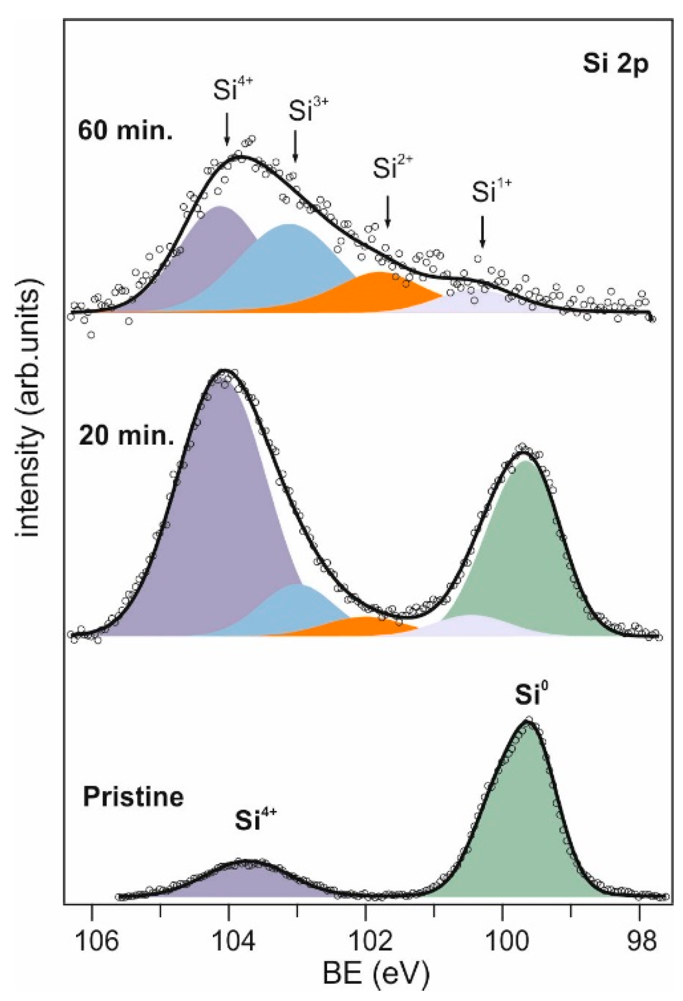
3.4. Role of the SiO2/Si Substrate

To investigate possible interactions of the target plasma with the substrate, the interface between as-deposited MoS2 and SiO2/Si substrate was carefully investigated via XPS. For this purpose, samples were deposited at 12 kV using two different deposition times (20 and 60 min), and annealed at 400 °C. The substrate-related Si 2p core level spectra of the two samples were compared to the spectrum of the pristine SiO2/Si substrate (see Figure 5).
The Si 2p core level spectrum of the pristine SiO2/Si substrate shows two typical peaks of 0 and 4+ oxidation states attributed to Si and SiO2 species (green and violet component located at 100.00 eV and 104.10 eV, respectively). The latter species originates from the native oxide film covering the pristine silicon substrate and having thicknesses of about 7–15 Å [27,28]. In the annealed MoS2 thin film deposited for 20 min, an intense SiO2 peak (Si4+) can be observed at about 104.10 eV and the Si0 peak is still present at 99.65 eV. Moreover, three additional components of 1+, 2+ and 3+ oxidation states were detected—namely, Si2O (BE = 100.45 eV, grey component), SiO (BE = 102.00 eV, orange component), and Si2O3 (BE = 103.00 eV, light blue component). By increasing the deposition time and hence obtaining a thicker film, the signal attributed to Si0 originating from the substrate completely disappeared, whereas the four oxide species are still detected at 100.45, 101.80, 103.10 and 104.10 eV, which are attributed to Si2O, SiO, Si2O3 and SiO2, respectively, in good agreement with literature values [29,30].

4. Discussion

XPS analysis of the sample deposited at 15 kV acceleration voltage (see Figure 2) proves that the detected Mo species corresponds to the 4+ oxidation state, and no oxidized species such as Mo6+ were detected, indicating successful synthesis of stochiometric MoS2 already in the as-deposited sample. Besides MoS2, S atoms that are not directly bound to Mo atoms such as in Mo−S−S species and/or an excess of free, elemental sulfur was found, which was gradually removed by increasing annealing temperatures (190–350 °C). Furthermore, the observed core level shift to lower BEs with annealing indicates a change of the electronic properties of MoS2, i.e., more p-type behavior in the annealed sample.
By varying the acceleration voltage in the range between 12–18 kV (see Figure 3), the amount of sulfur excess in the as-deposited sample only slightly changed, but reaches a minimum at 15 kV. This implies that 15 kV represents the optimized acceleration voltage in terms of target material use, i.e., it assures the most efficient ablation process without any target overheating. It should be noted that at 12 kV, the BE difference between Mo 3d5/2 and S 2p3/2 core levels is slightly different from typical 2H-MoS2, suggesting an ablation process with reduced efficiency in creating a proper plasma for material synthesis. Although further analysis is necessary, we assume that 12 kV does not enable a complete and efficient ablation process, leading to extraction of a plasma which is richer in the lighter species, i.e., sulfur. At an acceleration voltage of 18 kV instead, a preferential emission of sulfur might occur due to sublimation from MoS2. This is a further proof of empirical observations during IJD growth, i.e., the deposited energy does not only induce ablation but also strong target overheating (i.e., local explosion of large target pieces rather than a uniform plasma plume) leading to sulfur sublimation that increases the S concentration in the deposited film. However, by annealing in the range between 300–400 °C, the sulfur excess can be always removed, independent of the acceleration voltage. Therefore, the role of the energy of the pulsed electrons in the IJD deposition process is to influence the target material use and the discharge stability, but does not affect the properties of the film after annealing. Furthermore, the annealing step promotes MoS2 crystallization, as evidenced by the XRD pattern in Figure 4a, with a certain degree of disorder (Figure 4b).
The investigation of the interface between MoS2 and SiO2/Si substrate (see Figure 5) suggests the formation of new silicon oxide species on SiO2/Si during IJD growth. The corresponding processes and interfacial reactions during IJD are schematically shown in Figure 6. After ablation of the MoS2 target, the plasma plume is directed towards the substrate (Figure 6a) and mainly consists of Ar+ (due to Ar working gas) and ablated MoxSy species. Since the base pressure in the IJD chamber is in the order of 10−6 mbar, a partial pressure of water is present. These water molecules dissociate during IJD, giving rise to highly reactive oxygen radicals (O* in Figure 6a) in the plasma plume. Together with Ar+ and the ablated material, they are transferred to the substrate, where they react with the native SiO2 layer. As depicted in Figure 6b, the highly reactive O* and Ar+ species initially etch away the native oxide layer and further react with the underlying Si substrate, leading to the formation of new SiOx species (see Figure 6c). This means that during MoS2 growth, a complex oxide interface between silicon substrate and the growing MoS2 film is synthesized. The formation of silicon oxide interface has also been reported in MoS2 deposition via other PVD techniques, i.e., magnetron sputtering [31].

5. Conclusions

We present an original MoS2 synthesis approach based on IJD, a technique that could lead to TMDC synthesis compatible with large scale production. Among the different working conditions, we identified 15 kV acceleration voltage and 150 Hz deposition frequency as the best MoS2 growth parameters. The as-deposited films show the presence of stoichiometric MoS2 with an excess of free, elemental sulfur that can be removed by annealing in UHV at about 350–400 °C for 1 hour. Thermal treatment also improves the structural order, moving from amorphous to crystalline samples with a certain remaining degree of disorder. The harsh conditions during IJD synthesis lead to the formation of a complex silicon oxide interface, probably related to the presence of highly reactive oxygen species induced by ionization of water molecules. Such an effect can be avoided by using oxide-free substrates, such as Pt [31] or controlled by using lower base pressure in the deposition chamber, possibly in the 10−8/10−9 mbar range, where the water content is highly reduced.
The efficiency shown by IJD in MoS2 deposition paves the way for applications using different substrates and TMDCs, such as other sulfides and selenides, solving well-known problems regarding the selenization process.

Author Contributions

Conceptualization, M.V.N. and R.V.; methodology, M.T. and M.V.N.; validation, M.V.N. and A.C.; investigation, A.G. and A.C.; resources, R.V.; writing—original draft preparation, M.T.; writing—review and editing, M.T., M.V.N. and R.V.; visualization, M.T.; supervision, M.V.N. and R.V.; All authors have read and agreed to the published version of the manuscript.

Funding

This research received no external funding.

Acknowledgments

The authors gratefully acknowledge P. Bettotti and D. Maniglio for their assistance in AFM and SEM imaging, respectively. We thank P. Nozar for technical assistance and G. Tedeschi (Noivion S.r.l.) for IJD source support.

Conflicts of Interest

The authors declare no conflict of interest.

References

  1. Mak, K.F.; Lee, C.; Hone, J.; Shan, J.; Heinz, T.F. Atomically thin MoS2: A new direct-gap semiconductor. Phys. Rev. Lett. 2010, 105, 136805. [Google Scholar] [CrossRef] [PubMed] [Green Version]
  2. Samadi, M.; Sarikhani, N.; Zirak, M.; Zhang, H.; Zhang, H.; Moshfegh, A.Z. Group 6 transition metal dichalcogenide nanomaterials: Synthesis, applications and future perspectives. Nanoscale Horiz. 2018, 3, 90–204. [Google Scholar] [CrossRef] [PubMed]
  3. Xi, X.; Wang, Z.; Zhao, W.; Park, J.H.; Law, K.T.; Berger, H.; Forró, L.; Shan, J.; Mak, K.F. Ising pairing in superconducting NbSe2 atomic layers. Nat. Phys. 2016, 12, 139–143. [Google Scholar] [CrossRef] [Green Version]
  4. Radisavljevic, B.; Radenovic, A.; Brivio, J.; Giacometti, V.; Kis, A. Single-layer MoS2 transistors. Nat. Nanotechnol. 2011, 6, 147–150. [Google Scholar] [CrossRef] [PubMed]
  5. Liu, N.; Baek, J.; Kim, S.M.; Hong, S.; Hong, Y.K.; Kim, Y.S.; Kim, H.-S.; Kim, S.; Park, J. Improving the Stability of High-Performance Multilayer MoS2 Field-Effect Transistors. ACS Appl. Mater. Interfaces 2017, 9, 42943–42950. [Google Scholar] [CrossRef] [Green Version]
  6. Kim, J.S.; Yoo, H.W.; Choi, H.O.; Jung, H.T. Tunable volatile organic compounds sensor by using thiolated ligand conjugation on MoS2. Nano Lett. 2014, 14, 5941–5947. [Google Scholar] [CrossRef]
  7. Lee, J.; Dak, P.; Lee, Y.; Park, H.; Choi, W.; Alam, M.A.; Kim, S. Two-dimensional layered MoS₂ biosensors enable highly sensitive detection of biomolecules. Sci. Rep. 2014, 4, 7352. [Google Scholar] [CrossRef] [Green Version]
  8. Wang, W.; Panin, G.N.; Fu, X.; Zhang, L.; Ilanchezhiyan, P. MoS2 memristor with photoresistive switching. Sci. Rep. 2016, 6, 31224. [Google Scholar] [CrossRef] [Green Version]
  9. Nardi, M.V.; Timpel, M.; Ligorio, G.; Morales, N.Z.; Chiappini, A.; Toccoli, T.; Verucchi, R.; Ceccato, R.; Pasquali, L.; List-Kratochvil, E.J.W.; et al. Versatile and Scalable Strategy To Grow Sol−Gel Derived 2H-MoS2 Thin Films with Superior Electronic Properties: A Memristive Case. ACS Appl. Mater. Interfaces 2018, 10, 34392–34400. [Google Scholar] [CrossRef]
  10. Magda, G.Z.; Pető, J.; Dobrik, G.; Hwang, C.; Biró, L.P.; Tapasztó, L. Exfoliation of large-area transition metal chalcogenide single layers. Sci. Rep. 2015, 5, 14714. [Google Scholar] [CrossRef] [Green Version]
  11. Backes, C.; Higgins, T.M.; Kelly, A.; Boland, C.; Harvey, A.; Hanlon, D.; Coleman, J.N. Guidelines for Exfoliation, Characterization and Processing of Layered Materials Produced by Liquid Exfoliation. Chem. Mater. 2017, 29, 243–255. [Google Scholar] [CrossRef]
  12. Zhang, J.; Yang, A.; Wu, X.; van de Groep, J.; Tang, P.; Li, S.; Liu, B.; Shi, F.; Wan, J.; Li, Q.; et al. Reversible and selective ion intercalation through the top surface of few-layer MoS2. Nat. Commun. 2018, 9, 1–9. [Google Scholar] [CrossRef] [PubMed] [Green Version]
  13. Lee, Y.-H.; Zhang, X.-Q.; Zhang, W.; Chang, M.-T.; Lin, C.-T.; Chang, K.-D.; Yu, Y.-C.; Wang, J.T.-W.; Chang, C.-S.; Li, L.-J.; et al. Synthesis of Large-Area MoS2 Atomic Layers with Chemical Vapor Deposition. Adv. Mater. 2012, 24, 2320–2325. [Google Scholar] [CrossRef] [PubMed] [Green Version]
  14. George, A.S.; Mutlu, Z.; Ionescu, R.; Wu, R.J.; Jeong, J.S.; Bay, H.H.; Chai, Y.; Mkhoyan, K.A.; Ozkan, M.; Ozkan, C.S. Wafer scale synthesis and high resolution structural characterization of atomically thin MoS2 layers. Adv. Funct. Mater. 2014, 24, 7461–7466. [Google Scholar] [CrossRef]
  15. Gobbi, M.; Bonacchi, S.; Lian, J.X.; Bertolazzi, A.V.S.; Zyska, B.; Timpel, M.; Tatti, R.; Olivier, Y.; Hecht, S.; Nardi, M.V.; et al. Collective molecular switching in hybrid superlattices for light-modulated two-dimensional electronics. Nat. Commun. 2018, 9, 2661. [Google Scholar] [CrossRef]
  16. Siegel, G.; Venkata Subbaiah, Y.P.; Prestgard, M.C.; Tiwari, A. Growth of centimeter-scale atomically thin MoS2 films by pulsed laser deposition. APL Mater. 2015, 3, 056103. [Google Scholar] [CrossRef] [Green Version]
  17. Tao, J.; Chai, J.; Lu, X.; Wong, L.M.; Wong, T.I.; Pan, J.; Xiong, Q.; Chi, D.; Wang, S. Growth of wafer-scale MoS2 monolayer by magnetron sputtering. Nanoscale 2015, 7, 2497–2503. [Google Scholar] [CrossRef]
  18. Lotti, R.; Nozar, P.; Taliani, C. Device for Generating Plasma and for Directing an Flow of Electrons towards a Target. WO2010109297A2, 30 September 2010. [Google Scholar]
  19. Skocdopolova, L. Device for Generating Plasma and Directing an Electron Beam towards a Target. WO2013186697A3, 19 December 2013. [Google Scholar]
  20. Skocdopolova, L. Un Apparato ed un Metodo per la Generazione di Elettroni e di Plasma da un Getto di Gas. ITBO 20120320 A1, 11 December 2013. [Google Scholar]
  21. Heinrich, P.; Stoltenhoff, T.; Richter, P.; Kreye, H.; Richter, H. Method and System for Cold Gas Spraying. U.S. Patent US20040166247A1, 5 December 2006. [Google Scholar]
  22. Little, P.F.; von Engel, A. The hollow-cathode effect and the theory of glow discharges. Proc. R. Soc. A 1954, 224, 209–227. [Google Scholar]
  23. Mignuzzi, S.; Pollard, A.J.; Bonini, N.; Brennan, B.; Gilmore, I.S.; Pimenta, M.A.; Richards, D.; Roy, D. Effect of disorder on Raman scattering of single-layer MoS2. Phys. Rev. B-Condens. Matter Mater. Phys. 2015, 91, 1–7. [Google Scholar] [CrossRef] [Green Version]
  24. Li, H.; Zhang, Q.; Yap, C.C.R.; Tay, B.K.; Edwin, T.H.T.; Olivier, A.; Baillargeat, D. From bulk to monolayer MoS2: Evolution of Raman scattering. Adv. Funct. Mater. 2012, 22, 1385–1390. [Google Scholar] [CrossRef]
  25. Windom, B.C.; Sawyer, W.G.; Hahn, D.W. A Raman Spectroscopic Study of MoS2 and MoO3: Applications to Tribological Systems. Tribol. Lett. 2011, 42, 301–310. [Google Scholar] [CrossRef]
  26. Gołasa, K.; Grzeszczyk, M.; Bozek, R.; Leszczyński, P.; Wysmołek, A.; Potemski, M.; Babiński, A. Resonant Raman scattering in MoS2- From bulk to monolayer. Solid State Commun. 2014, 197, 53–56. [Google Scholar] [CrossRef]
  27. Morita, M.; Ohmi, T.; Hasegawa, E.; Kawakami, M.; Ohwada, M. Growth of native oxide on a silicon surface. J. Appl. Phys. 1990, 68, 1272–1281. [Google Scholar] [CrossRef]
  28. Song, Y.; Li, X.; Mackin, C.; Zhang, X.; Fang, W.; Palacios, T.; Zhu, H.; Kong, J. Role of interfacial oxide in high-efficiency graphene-silicon schottky barrier solar cells. Nano Lett. 2015, 15, 2104–2110. [Google Scholar] [CrossRef] [PubMed]
  29. Kim, S.; Kim, M.C.; Choi, S.H.; Kim, K.J.; Hwang, H.N.; Hwang, C.C. Size dependence of Si 2p core-level shift at Si nanocrystal/ SiO2 interfaces. Appl. Phys. Lett. 2007, 91, 1–4. [Google Scholar] [CrossRef]
  30. Renault, O.; Marlier, R.; Gely, M.; De Salvo, B.; Baron, T.; Hansson, M.; Barrett, N.T. Synchrotron radiation X-ray photoelectron spectroscopy of Si nanocrystals grown onto Al2O3/Si surfaces. Appl. Phys. Lett. 2005, 87, 163119. [Google Scholar] [CrossRef]
  31. Hussain, S.; Singh, J.; Vikraman, D.; Singh, A.K.; Iqbal, M.Z.; Khan, M.F.; Kumar, P.; Choi, D.C.; Song, W.; An, K.S.; et al. Large-area, continuous and high electrical performances of bilayer to few layers MoS2 fabricated by RF sputtering via post-deposition annealing method. Sci. Rep. 2016, 6, 1–13. [Google Scholar] [CrossRef] [Green Version]
Figure 1. (ac) Schematic sketch of the three main steps of ionized jet deposition (IJD) for thin film growth; (d) Photograph of the IJD chamber illustrating main discharge and target plasma during deposition with optimized operating parameters (discharge frequency f = 150 Hz, acceleration voltage V = 15 kV); (e) Photograph showing target overheating and formation of sparks during deposition with f > 250 Hz and/or V > 18 kV; the inlet displays a top view of the target’s surface after deposition with V = 18 kV.
Surfaces 03 00045 g001
Figure 2. IJD-MoS2 thin film deposited at 15 kV acceleration voltage: (a) XPS survey of as-deposited and annealed (T = 350 °C) thin film; (b) Mo 3d–S 2s and (c) S 2p core level spectra of as-deposited thin film and corresponding sample annealed at different temperatures T = 190, 280, 350 °C; deconvolved (d) Mo 3d–S 2s and (e) S 2p core level spectra of as-deposited and annealed (T = 350 °C) thin film.
Surfaces 03 00045 g002
Figure 3. Fitted (a) Mo 3d–S 2s and (b) S 2p core level spectra of IJD-MoS2 as-deposited with different acceleration voltages (12, 15 and 18 kV).
Surfaces 03 00045 g003
Figure 4. (a) XRD spectrum of IJD-MoS2 deposited at 18 kV and annealed at 380 °C; (b) µ-Raman spectra of as-deposited and annealed MoS2; (c) SEM and (d) AFM images of annealed MoS2.
Surfaces 03 00045 g004
Figure 5. Si 2p core level spectra of pristine SiO2/Si substrate and MoS2 thin film after 20- and 60-min deposition and annealing at 400 °C.
Surfaces 03 00045 g005
Figure 6. Schematic illustration of interfacial reactions in case of IJD-MoS2 on SiO2/Si substrate: (a) before ionized jet deposition; (b) initial etching of the SiO2 native oxide; (c) formation of complex SiOx surface and MoS2 thin film growth.
Surfaces 03 00045 g006
Table 1. Binding energy (BE), FWHM and S/Mo ratio of MoS2 single crystal and IJD-MoS2 deposited at 15 kV and annealed at different temperatures (TT).
SampleBE
(eV)
FWHMS/Mo 1
[2.0]
S/Mo 2
[2.0]
Mo 3d5/2S 2p3/2Mo 3dS 2p
single crystal229.55162.360.850.911.92
as-deposited228.99161.861.411.523.812.11
TT190228.96161.811.331.443.621.98
TT280228.72161.541.301.352.881.95
TT350228.62161.451.021.012.392.14
1 Both sulfur species have been considered. 2 Only the sulfur species attributed to MoS2 has been considered.
Table 2. Binding energy (BE), FWHM and S/Mo ratio of IJD-MoS2 samples deposited at 12, 15 and 18 kV, and corresponding annealed samples (TT).
Acceleration VoltageSampleBE
(eV)
FWHMS/Mo 1
[2.0]
Mo 3d5/2S 2p3/2Mo 3dS 2p
12 kVas-deposited229.08162.071.351.344.63
TT400228.34161.920.940.982.14
15 kVas-deposited228.99161.861.411.523.81
TT350228.62161.451.021.012.39
18 kVas-deposited229.09161.941.461.574.41
TT380228.62161.451.021.012.31
1 Both sulfur species have been considered.
Publisher’s Note: MDPI stays neutral with regard to jurisdictional claims in published maps and institutional affiliations.

