
Spontaneous Grafting of OH-Terminated Molecules on Si−H Surfaces via Si–O–C Covalent Bonding


1
School of Molecular and Life Sciences, Curtin Institute of Functional Molecules and Interfaces, Curtin University, Bentley, WA 6102, Australia
2
Australian Centre for Neutron Scattering, Australian Nuclear Science and Technology Organization (ANSTO), Lucas Heights, NSW 2234, Australia
*
Author to whom correspondence should be addressed.
Surfaces 2021, 4(1), 81-88; https://0-doi-org.brum.beds.ac.uk/10.3390/surfaces4010010
Submission received: 28 January 2021
/
Revised: 9 February 2021
/
Accepted: 10 February 2021
/
Published: 5 March 2021
Abstract
:The surface functionalization of oxide-free hydrogen-terminated silicon (Si−H) enables predictably tuning its electronic properties, by incorporating tailored functionality for applications such as photovoltaics, biosensing and molecular electronics devices. Most of the available chemical functionalization approaches require an external radical initiator, such as UV light, heat or chemical reagents. Here, we report forming organic monolayers on Si–H surfaces using molecules comprising terminal alcohol (–OH) groups. Self-assembled monolayer (SAM) formation is spontaneous, requires no external stimuli–and yields Si–O–C covalently bound monolayers. The SAMs were characterized by X-ray photoelectron spectroscopy (XPS) to determine the chemical bonding, by X-ray reflectometry (XRR) to determine the monolayers thicknesses on the surface and by atomic force microscopy (AFM) to probe surface topography and surface roughness. The redox activity and the electrochemical properties of the SAMs were studied using cyclic voltammetry (CV) and electrochemical impedance spectroscopy (EIS). The availability and the ease of incorporating OH groups in organic molecules, makes this spontaneous grafting as a reliable method to attach molecules to Si surfaces in applications ranging from sensing to molecular electronics where incorporating radical initiator setups is not accessible.
1. Introduction
Silicon (Si) is the most commonly used semiconductor in the current electronic devices’ technologies, due to its low cost, abundance and intriguing semiconducting properties [1,2,3,4,5]. Although, the semiconducting electronic properties of Si are desired, the surface of Si is covered, at ambient conditions, by an electrically insulating thin layer of oxide that masks its electronic properties [6,7,8,9]. In addition, modifying Si with self–assembled monolayers (SAMs) has received much attention due to its applications in many fields including biosensors [10,11], energy harvesting devices [12,13,14] and molecular electronics [15,16,17].
Earlier, hydroxyl-terminated molecules such as alkyl silanols have been utilized to form self-assembled monolayers (SAMs) on SiOx surfaces. Although this method is rapid, the formed SAMs suffered from poor uniformity due to the formation of undesired polysilanol networks that hinder the electron transfer at the molecule-electrode interface [2,18]. Thus, modification of the Si surfaces with molecules while avoiding the interference of the insulating surface oxides is desired for better performing devices and wider range of application. In this context, crystalline Si requires etching the oxide layer by fluoride ions (e.g., HF and NH4F) in order to expose the Si–H surface and its semiconducting properties but etched Si–H surfaces have short lifespan stability towards re-oxidation and require surface functionalization to protect them against oxidation.
During last two decades, oxide-free silicon (Si−H) surface modification with organic molecules has emerged as a viable path in tuning the electronic properties of Si, in addition to protecting the semiconductor from oxidation. In most cases, forming SAMs on Si–H requires a catalyst to initiate a radical on the Si surface (or on the molecule), followed by a polymerization chain reaction that forms a complete molecular film on the surface [19,20,21,22,23,24]. Typical functionalization molecules are alkenes or alkynes, which form covalent Si−C bonding with Si surfaces when aided by UV light [25,26,27], heat [9,27,28] or harsh chemical reagents [28,29,30]. Although, these SAMs are of good quality, the requirement of UV or heat sources adds complications, which may hinder specific applications, such as in the field of molecular electronics where the incorporation of bulky setups is often not viable [15,16,31,32,33].
Recently, we have demonstrated that spontaneous nanoscale corrosion of Si–H surfaces leads to disulfide bond breaking and enables the formation of high-quality SAMs of thiols and disulfides on Si [16,34]. In this study, we turn our attention to OH contact groups as they are commonly available functionalities that could broaden the source of the organic molecules that can form monolayers on Si. Khung et al. have used thermal and UV-assisted protocols to attach OH-terminated alkynes to Si(111)–H surfaces, showing that thermal energy can catalyze the grafting process through generating reactive silyl radicals that form a Si–O–C linkage via nucleophilic reaction between the OH group of organic molecule and the Si–H surface [35]. Also, Fontanesi et al. [36] have used ferrocene methanol to form a redox active monolayer on Si–H surfaces using heat for two hours at 56 °C. Also, in molecular electronics studies, rigid norbornylogous bridge (NB) molecules are widely used. On metals, these NBs form SAMs with restricted molecular rotations [31,33,37], as compared to alkane monolayers, which are the typical molecules used to form monolayers on surfaces.
Here, we test whether molecules with OH groups can spontaneously react with Si–H surfaces. We use ferrocene methanol which is a redox active molecule terminated by one OH groups and an NB molecule terminated by two OH groups (Figure 1). We successfully demonstrate that spontaneous grafting of OH-terminated molecules enables forming SAMs on Si–H via Si–O–C covalent bonding without any external catalysis. The OH-functionalized surfaces were characterized using X-ray photoelectron spectroscopy (XPS), to investigate the chemical bonding, with AFM to study the surface topography and with X-ray reflectometry (XRR) to measure the monolayer thickness. Cyclic voltammetry (CV) and electrochemical impedance spectroscopy (EIS) are used to electrochemically assess the formation of the monolayers.
2. Materials and Methods
2.1. Chemicals and Reagents
Sulfuric acid (Puranal TM, 95–97%), hydrogen peroxide (30 wt.% in water), ammonium fluoride (Puranal TM, 40 wt.% in water) and ferrocene methanol (97%) were purchased from Sigma Aldrich (New South Wales, Australia) and used without any further purification. The synthesis of norbornylogous bridge (NB) 2 has been reported elsewhere [37]. Dichloromethane (DCM), isopropyl alcohol (IP) and ethanol were purified by distillation before use. Silicon wafers were purchased from Siltronix, S.A.S. (Archamps, France). The p-type silicon was highly doped (boron), with nominal resistivity between 0.007 and 0.013 Ω cm and wafer thickness of 500 ± 25 µm. Wafers were oriented ±0.5° away from the (111) plane. Milli-Q water (>18 MΩ cm) was used for all cleaning procedures and to prepare electrolytic solutions.
2.2. Surface Preparation and Functionalization
P-type Si wafers were cut into samples of approximately 1×1 cm, washed with DCM, IP and water, then treated with in a piranha solution for 30 min at 130 °C (a mixture of concentrated sulfuric acid and 30% hydrogen peroxide, 3:1, v:v, respectively). The wafers were then rinsed with water before being etched for 13 min in a deoxygenated solution of ammonium fluoride (40%). After ammonium fluoride etching, the Si–H surfaces were rinsed quickly with Milli-Q water once, followed by DCM three times and finally blown with N2 gas before dipping in the grafting solution. The spontaneous grafting involved only dipping the Si electrode in a 5 mM solution of 1 dissolved in DCM or 2 dissolved in dimethylformamide (DMF) for 12 h to allow the SAM formation. The electrodes were then washed with DCM, followed by drying under a stream of Ar gas before further analysis.
2.3. Atomic Force Microscopy Imaging
Atomic force microscopy (AFM) images were acquired using a Bruker dimension microscope, operating in tapping mode. The FastScan head was used and the resolution was set to 512 points/line with scan rate of 0.5 Hz and all images were recorded using silicon nitride cantilevers (TESPA from Bruker (Singapore), with a spring constant of 20 N m−1) at room temperature, in air. Bruker’s Nanoscope Software was used to analyze the surface roughness by measuring the root mean square, Rq, deviation in the height of the Si surfaces.
2.4. X-ray Photoelectron Spectroscopy (XPS) Analysis
XPS measurements were performed on a Kratos Axis Ultra DLD spectrometer (Shimadzu, Manchester, UK), using a monochromatic Al-Kα (1486.6 eV) irradiation source operating at 150 W. Spectra of Si 2p (90–110 eV), C 1s (277–300 eV) and S 2p (163−164 eV) were taken in normal emission, with the main chamber at or below 7 × 10⁻⁹ Torr. Data files were processed using CasaXPS© software and the reported XPS energies are binding energies expressed in eV. After background subtraction (Shirley), spectra were fitted with Voigt functions. To correct for energy shifts caused by adventitious charging, all peak energies were corrected by applying a rigid shift to bring the C 1s emission to 284.7 eV.
2.5. X-ray Reflectometry (XRR) Analysis
A Panalytical Ltd. X’Pert Pro (ANSTO, Australia) was used to record XRR spectra at the silicon–air interface. The spectrometer was fitted with a Cu Kα (λ = 1.54 Å) source and the X-ray beam was focused using a Göbel mirror and collimated using fixed slits of 0.1 mm. Further details for the XRR measurements can be found in the supporting information.
2.6. Electrochemical Measurements
All electrochemical measurements were performed with a CHI650 electrochemical workstation (CH Instruments, Austin, TX, USA), using a conventional three-electrode single-compartment cell. The functionalized Si surface act as the working electrode versus a of Ag/AgCl reference electrode in a saturated solution of potassium chloride (KCl) and a platinum wire as the counter electrode. CV measurements were carried out in aqueous solution of 1 M sodium perchlorate (NaClO4), and EIS measurement are carried out in 1 mM solution of hexaammineruthenium(III) chloride (in 10 mM KCl) All potentials are reported against the Ag/AgCl reference electrode.
3. Results and Discussion
3.1. Surface Characterization
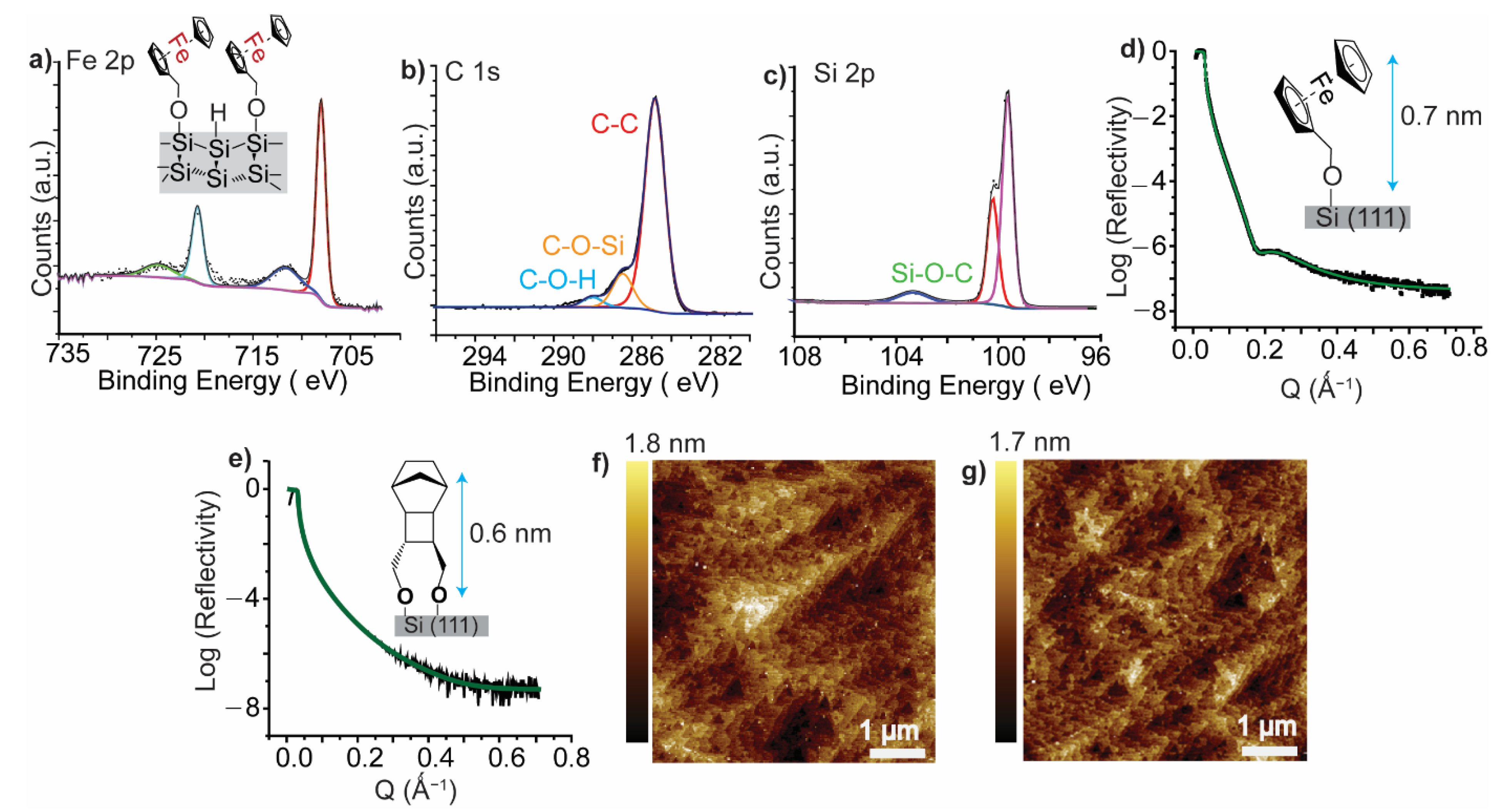
Figure 2a shows the Fe 2p signal from the iron metal center in the ferrocene moiety of 1 on p-type Si with two spin-orbit splits. The peaks at 707.2 eV and 720.3 eV are assigned to the Fe 2p3/2 and Fe 2p1/2, for low and high energy spins, respectively, fitted with a Shirley background subtraction and an energy difference of 13.1 eV. The peaks at 711.6 eV and 724.7 eV correspond to the Fe 2p3/2 and Fe 2p1/2 for low and high energy emissions, respectively, from the Fe+2 spins. Figure 2b shows the high-resolution C 1s spectrum of 1 fitted into 3 peaks (Figure 2b). The peak at 284.8 eV is ascribed to the C–C bonding, the peak at 286.5 eV is assigned to the carbon adjacent to the Si-bound hydroxyl group (Si–O–C) and the peak at 288.0 eV corresponds to the carbon adjacent to a free hydroxyl group that is probably physically adsorbed (HO–C–). Further, fitting the Si 2p high resolution envelope showed three peaks, with the main emission composed of one spin-orbit split with two peaks at 99.7 eV and 100.0 eV, corresponding to the Si 2p3/2 and Si 2p1/2 for low and high energy spins, respectively. The peak at 103.0 eV is assigned to the Si that bound to 1 via Si–O–C covalent bonds (Figure 2c). No emission was observed at 103 eV for a Si–H surface that was analyzed after etching and before the spontaneous grafting step (Figure S1). Thus, XPS analysis of the SAM of 1 on Si–H surfaces indicates a covalent C–O–Si bonding. Detailed XPS analysis for the Si 2p signal from a bare Si–H surface and an Si–H surface that is functionalized with 1 shows that the Si 2p emission, from the Si–O–R functionalized surface, is centered at BE of 99.7 eV while the Si 2p emission from bare Si–H is centered at 99.5 eV (Figure S2). This is suggests that chemical modification of Si–H surfaces with organic molecules lead to orbital hybridization between the energy levels of Si and that of the molecule creating new electronic states a at the interface, consistent with observations for the effect of other monolayers on the semiconducting properties of Si [38]. XRR analysis for SAMs of 1 and 2 on Si–H surface demonstrated the presence of a molecular film on the surface with a thickness comparable to the theoretical lengths of the molecules used. Figure 2d, e shows molecular films of 0.7 nm and 0.6 nm thickness for the SAM formed from 1 and 2, respectively. XRR analysis details and fitting parameters are discussed in supporting information (Table S1). AFM imaging for the functionalized Si–H surfaces shows smooth edges and individual flat terraces of roughness ~0.2 nm (Figure 2e,f), consistent with results from typical alkyne/alkene monolayers formed on Si–H [16,34]. Further, AFM images for non-functionalized Si–H surfaces (Figure S3) showed minimal change after functionalization demonstrating that the monolayers are formed smoothly without causing any dramatic changes to the crystalline Si surface.
3.2. Electrochemical Characterization of The Formed Monolayers
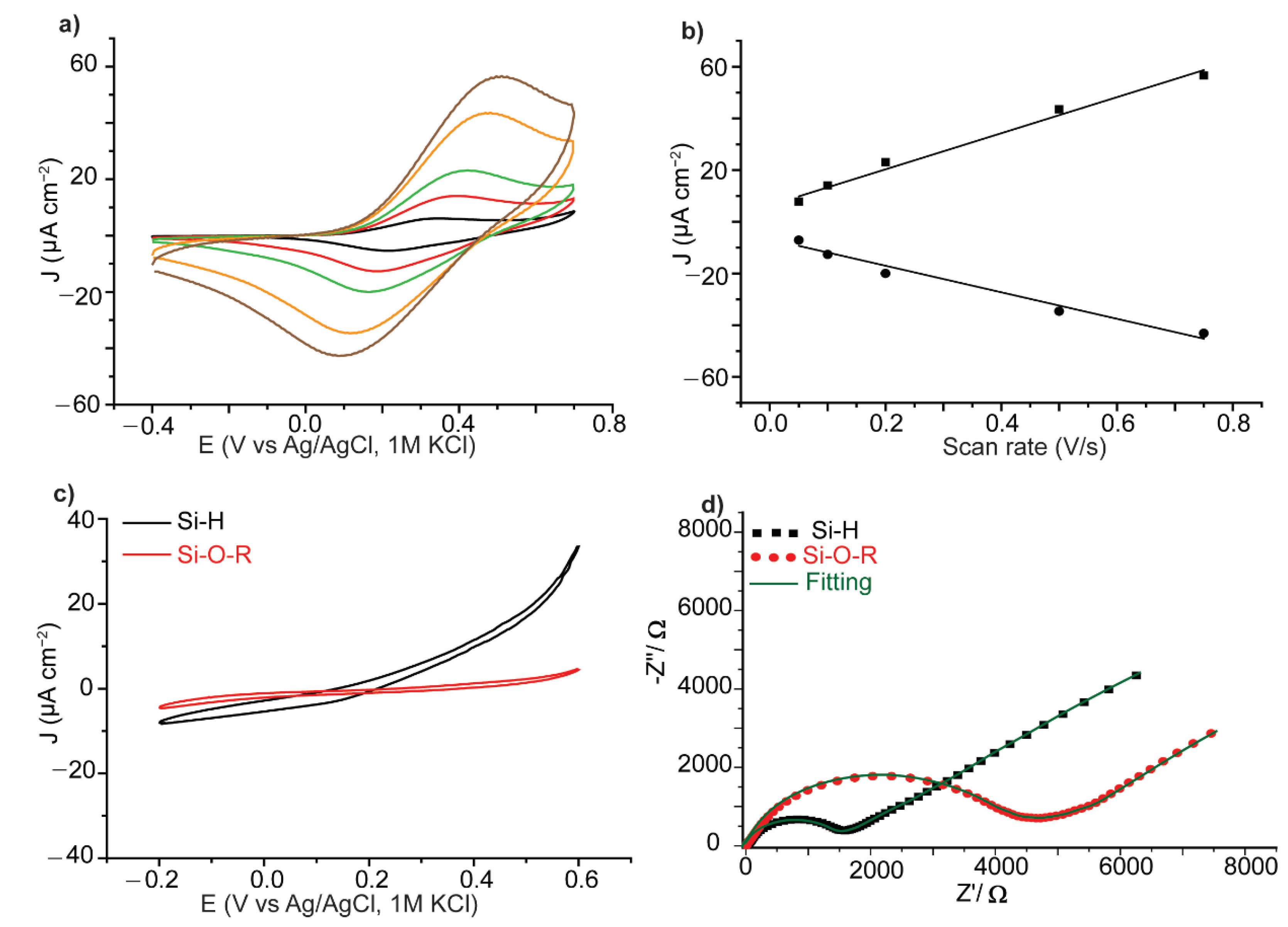
The SAMs on 1 and 2 formed by spontaneous grafting for 12 h at ambient conditions, are characterized by cyclic voltammetry (CV) and electrochemical impedance spectroscopy (EIS). Figure 3a shows CVs for the formed SAM of 1, at different scan rates, with the characteristic redox peaks of the ferrocene moiety, consistent with voltammetry measurements for monolayers formed on Si–H by other means such as UV light that was reported by Fontanesi et al. [36]. The evolution of the peak current versus the scan rates shows a linear relationship, indicating the formation of a surface-bound system. The CV for the SAM of 2 on Si–H showed stable voltammetric current in contrary to the unmodified Si–H surface tested in the same electrolyte. The latter showed an increase in the voltammetric current and is attributed to anodic oxidation of the Si surface. This suggests that the SAM of 2 protects the Si surface form oxidation, within the potential window investigated, in aqueous medium (Figure 3c). EIS measurements in the presence of a redox active ruthenium hexamine solution showed that upon the formation of a SAM of 2 the resistance increases, indicating that the monolayer is packed in way that relatively blocks the redox active solution from reaching the electrode surface and consequently increasing the resistance of 2 on Si showed high electrode resistance. The Nyquist plots in Figure 3d are fitted to equivalent circuit models using the complex non-linear least-square (CNLS) technique using the Randles circuits (Figure S4) which models redox-active species in a diffusion system. Cdl represents the double layer capacitance, Rs and Rct represent the solution and charge transfer resistances, respectively and Ws1 represent the Warburg diffusion element of the redox species in the electrolyte solution. Rct of ~1187 Ω and ~4571 Ω for the bare Si–H and the functionalized Si surface respectively, is expected on the basis that a monolayer can partially block charge transfer at the interface and therefore increase the charge transfer resistance.
We conclude here that the spontaneous reaction of OH groups with H–terminated Si is a highly efficient approach to prepare molecular films on Si–H surfaces. While the mechanism of the reaction is not yet well understood, the covalent attachment has been previously demonstrated for thermal grafting of OH–terminated molecules and the spontaneous grafting of graphene oxide films on Si (111) surfaces [39]. In the former, the reaction is thought to be due to a nucleophilic attack of the O lone pair on the Si (111) followed by the loss of H2 gas to yield Si–O–R monolayers [36]. In the latter, the reaction was explained by a dehydration reaction forming a Si–C=C monolayers [40]. Our XPS results demonstrate the presence of Si–O–C at the interface which is not accompanied by SiOx as demonstrated by AFM. We therefore lean toward a mechanism that involves nucleophilic attack by the O lone pair on Si surface holes. Further work will need to test the effect of the Si doping type (p or n-type) and concentration, as well as the effect of the solvent on the efficiency of the grafting. These parameters will necessarily change the concentration of surface holes which, in turn, will affect the efficiency of the nucleophilic attack.
4. Conclusions
We have demonstrated the formation of SAMs on Si by simply incubating freshly etched Si–H surfaces in a solution containing OH-terminated molecules. The grafting process is spontaneous and does not require any catalyst, a significant advantage over more established Si modification chemistry that typically requires an external radical initiator such as UV, heat or chemical reagents. The fact that OH groups are widely accessible and can be easily incorporated in molecules, makes this spontaneous grafting method appealing for connecting molecules to Si surfaces in applications ranging from sensing to molecular electronics.
Supplementary Materials
The following are available online at https://0-www-mdpi-com.brum.beds.ac.uk/2571-9637/4/1/10/s1, Figure S1: Si 2p high resolution spectrum for a freshly prepared Si–H surface, after the etching step. Figure S2: XPS analysis showing high resolution Si 2p signal from a pure Si–H surface versus a Si surface functionalized with 1. Figure S3: AFM topography images with large scan area (a) and small scan area (b) for Si–H surface without SAMs. Figure S4: Equivalent circuit for the Nyquist plots of the EIS measured for the SAM of 2 on Si–H and the fresh Si–H surfaces. Table S1: Fitted thicknesses, surface roughness, and fitted SLD for SAMs formed from 1 and 2 on Si (111)–H as determined from XRR data.
Author Contributions
N.D. conceived the project. E.M.D. performed all the surface preparation, AFM imaging, XPS and electrochemical experiments and analyzed the data. A.P.L.B. performed the XRR measurements. S.C. helped in data analysis. E.M.D. and N.D. wrote the manuscript with contributions from other authors. All authors discussed and interpreted the results. All authors have read and agreed to the published version of the manuscript.
Funding
N.D. and S.C. thank the Australian Research Council for a Discovery Project grant (DP190100735).
Institutional Review Board Statement
Not applicable.
Informed Consent Statement
Not applicable.
Data Availability Statement
Data is contained within the article or Supplementary Material.
Conflicts of Interest
The authors declare no conflict of interest.
References
- Aswal, D.K.; Lenfant, S.; Guerin, D.; Yakhmi, J.V.; Vuillaume, D. Self assembled monolayers on silicon for molecular electronics. Anal. Chim. Acta 2006, 568, 84–108. [Google Scholar] [CrossRef] [PubMed]
- Gooding, J.J.; Ciampi, S. The molecular level modification of surfaces: From self-assembled monolayers to complex molecular assemblies. Chem. Soc. Rev. 2011, 40, 2704–2718. [Google Scholar] [CrossRef] [PubMed] [Green Version]
- Halik, M.; Hirsch, A. The Potential of Molecular Self-Assembled Monolayers in Organic Electronic Devices. Adv. Mater. 2011, 23, 2689–2695. [Google Scholar] [CrossRef] [PubMed]
- Hwang, S.-W.; Tao, H.; Kim, D.-H.; Cheng, H.; Song, J.-K.; Rill, E.; Brenckle, M.A.; Panilaitis, B.; Won, S.M.; Kim, Y.-S. A physically transient form of silicon electronics. Science 2012, 337, 1640–1644. [Google Scholar] [CrossRef] [PubMed] [Green Version]
- Sun, L.; Diaz-Fernandez, Y.A.; Gschneidtner, T.A.; Westerlund, F.; Lara-Avila, S.; Moth-Poulsen, K. Single-molecule electronics: From chemical design to functional devices. Chem. Soc. Rev. 2014, 43, 7378–7411. [Google Scholar] [CrossRef] [Green Version]
- Fortunato, E.; Barquinha, P.; Martins, R. Oxide semiconductor thin-film transistors: A review of recent advances. Adv. Mater. 2012, 24, 2945–2986. [Google Scholar] [CrossRef]
- Nohira, T.; Yasuda, K.; Ito, Y. Pinpoint and bulk electrochemical reduction of insulating silicon dioxide to silicon. Nat. Mater. 2003, 2, 397–401. [Google Scholar] [CrossRef] [PubMed]
- Onclin, S.; Ravoo, B.J.; Reinhoudt, D.N. Engineering Silicon Oxide Surfaces Using Self-Assembled Monolayers. Angew. Chem. Int. Ed. 2005, 44, 6282–6304. [Google Scholar] [CrossRef] [PubMed]
- Thissen, P.; Seitz, O.; Chabal, Y.J. Wet chemical surface functionalization of oxide-free silicon. Prog. Surf. Sci. 2012, 87, 272–290. [Google Scholar] [CrossRef]
- Michaels, P.; Alam, M.T.; Ciampi, S.; Rouesnel, W.; Parker, S.G.; Choudhury, M.H.; Gooding, J.J. A robust DNA interface on a silicon electrode. Chem. Commun. 2014, 50, 7878–7880. [Google Scholar] [CrossRef] [PubMed] [Green Version]
- Schreiber, F. Self-assembled monolayers: From simple model systems to biofunctionalized interfaces. J. Phys. Condens. Matter 2004, 16, R881–R900. [Google Scholar] [CrossRef]
- Leonardi, F. Self-Assembled Monolayers (SAMs) in Organic Field-Effect Transistors. Ph.D. Dissertation, Alma Mater Studiorum Università di Bologna, Bologna, Italy, 2014. [Google Scholar]
- See, P.; Paul, D.J.; Hollander, B.; Mantl, S.; Zozoulenko, I.V.; Berggren, K. High performance Si/Si/sub 1-x/Gex resonant tunneling diodes. IEEE Electron Device Lett. 2001, 22, 182–184. [Google Scholar] [CrossRef]
- Wayner, D.D.M.; Wolkow, R.A. Organic modification of hydrogen terminated silicon surfaces. J. Chem. Soc. Perkin Trans. 2 2002, 23–34. [Google Scholar] [CrossRef]
- Aragonès, A.C.; Darwish, N.; Ciampi, S.; Sanz, F.; Gooding, J.J.; Díez-Pérez, I. Single-molecule electrical contacts on silicon electrodes under ambient conditions. Nat. Commun. 2017, 8, 15056. [Google Scholar] [CrossRef]
- Peiris, C.R.; Ciampi, S.; Dief, E.M.; Zhang, J.; Canfield, P.J.; Le Brun, A.P.; Kosov, D.S.; Reimers, J.R.; Darwish, N. Spontaneous S–Si bonding of alkanethiols to Si(111)–H: Towards Si–molecule–Si circuits. Chem. Sci. 2020, 11, 5246–5256. [Google Scholar] [CrossRef]
- Peiris, C.R.; Vogel, Y.B.; Le Brun, A.P.; Aragonès, A.C.; Coote, M.L.; Díez-Pérez, I.; Ciampi, S.; Darwish, N. Metal–Single-Molecule–Semiconductor Junctions Formed by a Radical Reaction Bridging Gold and Silicon Electrodes. J. Am. Chem. Soc. 2019, 141, 14788–14797. [Google Scholar] [CrossRef]
- Jung, G.-Y.; Li, Z.; Wu, W.; Chen, Y.; Olynick, D.L.; Wang, S.-Y.; Tong, W.M.; Williams, R.S. Vapor-Phase Self-Assembled Monolayer for Improved Mold Release in Nanoimprint Lithography. Langmuir 2005, 21, 1158–1161. [Google Scholar] [CrossRef] [PubMed]
- Buriak, J.M. Illuminating Silicon Surface Hydrosilylation: An Unexpected Plurality of Mechanisms. Chem. Mater. 2014, 26, 763–772. [Google Scholar] [CrossRef]
- Buriak, J.M.; Sikder, M.D.H. From Molecules to Surfaces: Radical-Based Mechanisms of Si–S and Si–Se Bond Formation on Silicon. J. Am. Chem. Soc. 2015, 137, 9730–9738. [Google Scholar] [CrossRef] [PubMed]
- Hu, M.; Hauger, T.C.; Olsen, B.C.; Luber, E.J.; Buriak, J.M. UV-Initiated Si–S, Si–Se, and Si–Te Bond Formation on Si(111): Coverage, Mechanism, and Electronics. J. Phys. Chem. C 2018, 122, 13803–13814. [Google Scholar] [CrossRef] [Green Version]
- Li, Y.; Calder, S.; Yaffe, O.; Cahen, D.; Haick, H.; Kronik, L.; Zuilhof, H. Hybrids of Organic Molecules and Flat, Oxide-Free Silicon: High-Density Monolayers, Electronic Properties, and Functionalization. Langmuir 2012, 28, 9920–9929. [Google Scholar] [CrossRef]
- Sieval, A.B.; Demirel, A.L.; Nissink, J.W.M.; Linford, M.R.; van der Maas, J.H.; de Jeu, W.H.; Zuilhof, H.; Sudhölter, E.J.R. Highly Stable Si−C Linked Functionalized Monolayers on the Silicon (100) Surface. Langmuir 1998, 14, 1759–1768. [Google Scholar] [CrossRef]
- Sun, Q.Y.; de Smet, L.C.; van Lagen, B.; Wright, A.; Zuilhof, H.; Sudholter, E.J. Covalently attached monolayers on hydrogen-terminated Si(100): Extremely mild attachment by visible light. Angew. Chem. Int. Ed. Engl. 2004, 43, 1352–1355. [Google Scholar] [CrossRef] [PubMed]
- Sieval, A.B.; Linke, R.; Zuilhof, H.; Sudhölter, E.J.R. High-Quality Alkyl Monolayers on Silicon Surfaces. Adv. Mater. 2000, 12, 1457–1460. [Google Scholar] [CrossRef]
- Ahmad, S.A.A.; Ciampi, S.; Parker, S.G.; Gonçales, V.R.; Gooding, J.J. Forming Ferrocenyl Self-Assembled Monolayers on Si(100) Electrodes with Different Alkyl Chain Lengths for Electron Transfer Studies. ChemElectroChem 2019, 6, 211–220. [Google Scholar] [CrossRef]
- Ciampi, S.; Harper, J.B.; Gooding, J.J. Wet chemical routes to the assembly of organic monolayers on silicon surfaces via the formation of Si-C bonds: Surface preparation, passivation and functionalization. Chem. Soc. Rev. 2010, 39, 2158–2183. [Google Scholar] [CrossRef] [PubMed] [Green Version]
- Sun, J.; Deng, L. Cobalt Complex-Catalyzed Hydrosilylation of Alkenes and Alkynes. ACS Catal. 2016, 6, 290–300. [Google Scholar] [CrossRef]
- Boukherroub, R.; Wayner, D.D.M. Controlled Functionalization and Multistep Chemical Manipulation of Covalently Modified Si(111) Surfaces1. J. Am. Chem. Soc. 1999, 121, 11513–11515. [Google Scholar] [CrossRef]
- Boukherroub, R.; Morin, S.; Bensebaa, F.; Wayner, D.D.M. New Synthetic Routes to Alkyl Monolayers on the Si(111) Surface1. Langmuir 1999, 15, 3831–3835. [Google Scholar] [CrossRef]
- Darwish, N.; Aragonès, A.C.; Darwish, T.; Ciampi, S.; Diez-Perez, I. Multi-responsive photo-and chemo-electrical single-molecule switches. Nano Lett. 2014, 14, 7064–7070. [Google Scholar] [CrossRef]
- Darwish, N.; Eggers, P.K.; Ciampi, S.; Tong, Y.; Ye, S.; Paddon-Row, M.N.; Gooding, J.J. Probing the effect of the solution environment around redox-active moieties using rigid anthraquinone terminated molecular rulers. J. Am. Chem. Soc. 2012, 134, 18401–18409. [Google Scholar] [CrossRef] [PubMed]
- Aragonès, A.C.; Darwish, N.; Im, J.; Lim, B.; Choi, J.; Koo, S.; Díez-Pérez, I. Fine-Tuning of Single-Molecule Conductance by Tweaking Both Electronic Structure and Conformation of Side Substituents. Chem.-Eur. J. 2015, 21, 7716–7720. [Google Scholar] [CrossRef] [PubMed]
- Dief, E.M.; Vogel, Y.B.; Peiris, C.R.; Le Brun, A.P.; Gonçales, V.R.; Ciampi, S.; Reimers, J.R.; Darwish, N. Covalent Linkages of Molecules and Proteins to Si–H Surfaces Formed by Disulfide Reduction. Langmuir 2020, 36, 14999–15009. [Google Scholar] [CrossRef] [PubMed]
- Khung, Y.L.; Ngalim, S.H.; Scaccabarozi, A.; Narducci, D. Thermal and UV Hydrosilylation of Alcohol-Based Bifunctional Alkynes on Si (111) surfaces: How surface radicals influence surface bond formation. Sci. Rep. 2015, 5, 11299. [Google Scholar] [CrossRef] [PubMed] [Green Version]
- Fontanesi, C.; Como, E.D.; Vanossi, D.; Montecchi, M.; Cannio, M.; Mondal, P.C.; Giurlani, W.; Innocenti, M.; Pasquali, L. Redox-Active Ferrocene grafted on H-Terminated Si(111): Electrochemical Characterization of the Charge Transport Mechanism and Dynamics. Sci. Rep. 2019, 9, 8735. [Google Scholar] [CrossRef]
- Darwish, N.; Díez-Pérez, I.; Da Silva, P.; Tao, N.; Gooding, J.J.; Paddon-Row, M.N. Observation of Electrochemically Controlled Quantum Interference in a Single Anthraquinone-Based Norbornylogous Bridge Molecule. Angew. Chem. Int. Ed. 2012, 51, 3203–3206. [Google Scholar] [CrossRef]
- Hacker, C.A. Modifying electronic properties at the silicon–molecule interface using atomic tethers. Solid-State Electron. 2010, 54, 1657–1664. [Google Scholar] [CrossRef]
- Rahpeima, S.; Dief, E.M.; Peiris, C.R.; Ferrie, S.; Duan, A.; Ciampi, S.; Raston, C.L.; Darwish, N. Reduced graphene oxide–silicon interface involving direct Si–O bonding as a conductive and mechanical stable ohmic contact. Chem. Commun. 2020, 56, 6209–6212. [Google Scholar] [CrossRef] [PubMed]
- Chan Lee, S.; Some, S.; Wook Kim, S.; Jun Kim, S.; Seo, J.; Lee, J.; Lee, T.; Ahn, J.-H.; Choi, H.-J.; Chan Jun, S. Efficient Direct Reduction of Graphene Oxide by Silicon Substrate. Sci. Rep. 2015, 5, 12306. [Google Scholar] [CrossRef] [Green Version]
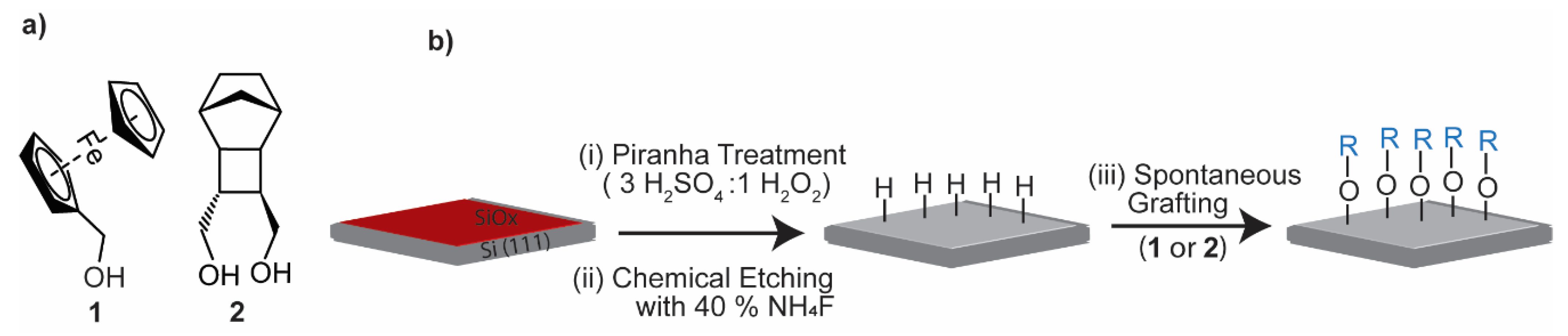
Figure 1.
Schematic of the modification of the Si–H surfaces with OH-terminated molecules 1 and 2. (a) Structure of the monolayer-forming molecules. (b) Schematic of the surface functionalization process: (i) cleaning organic contamination by Piranha solution; (ii) SiOx etching with ammonium fluoride solutions; and (iii) spontaneous grafting of OH-terminated molecules to the Si–H surface with formation of covalent Si–O–C bonds.

Figure 2.
Surface characterization of the formed monolayers. (a–c) High resolution X-ray photoelectron spectroscopy (XPS) spectra for Fe 2p (a), C 1s (b) and Si 2p spectrum(c) for a monolayer of 1 on Si–H, suggesting covalent bond formation by Si–O–C contacts as demonstrated in the Si 2p and C 1s fittings. (d,e) X-ray reflectometry (XRR) measurements for the monolayer of 1 (d) and 2 (e) on Si–H. Black line is raw data and green line represents the best fit. XRR fitting parameters are shown in supporting information (Table S1). (f,g) Atomic force microscopy (AFM) topography images for Si (111)–H surface functionalized with 1 (f) and with 2 (g).

Figure 3.
Electrochemical characterization of the formed self-assembled monolayers (SAMs). (a) Cyclic voltammograms at different scan rates for a SAM of 1 on Si–H, black: 0.05 Vs−1, red: 0.1 Vs−1, green: 0.2 Vs−1, orange: 0.5 Vs−1, brown: 0.75 Vs−1. (b) Evolution of the peak current vs scan rates, dots are data points and lines are linear fitting. (c) Cyclic voltammetry (CV) wave for the formed SAM of 2 on Si–H (red) as compared to a bare Si–H electrode in NaClO4 (1.0 M) electrolyte, showing that the bare Si is more prone to oxidation than the monolayer-protected surface. (d) Nyquist plot of the electrochemical impedance spectroscopy (EIS). measurement for a SAM of 2 on Si–H, measured in a solution of ruthenium hexamine (10 mM) in 0.5 M KCl. Dots (red and black) represent the raw data and green line represents the Randles circuit fitting. Rct for Si–H ~ 1187 Ω and for Si–O–R surface ~4571 Ω.

Publisher’s Note: MDPI stays neutral with regard to jurisdictional claims in published maps and institutional affiliations. |
© 2021 by the authors. Licensee MDPI, Basel, Switzerland. This article is an open access article distributed under the terms and conditions of the Creative Commons Attribution (CC BY) license (http://creativecommons.org/licenses/by/4.0/).
Share and Cite
MDPI and ACS Style
Dief, E.M.; Brun, A.P.L.; Ciampi, S.; Darwish, N. Spontaneous Grafting of OH-Terminated Molecules on Si−H Surfaces via Si–O–C Covalent Bonding. Surfaces 2021, 4, 81-88. https://0-doi-org.brum.beds.ac.uk/10.3390/surfaces4010010
AMA Style
Dief EM, Brun APL, Ciampi S, Darwish N. Spontaneous Grafting of OH-Terminated Molecules on Si−H Surfaces via Si–O–C Covalent Bonding. Surfaces. 2021; 4(1):81-88. https://0-doi-org.brum.beds.ac.uk/10.3390/surfaces4010010
Chicago/Turabian StyleDief, Essam M., Anton P. Le Brun, Simone Ciampi, and Nadim Darwish. 2021. "Spontaneous Grafting of OH-Terminated Molecules on Si−H Surfaces via Si–O–C Covalent Bonding" Surfaces 4, no. 1: 81-88. https://0-doi-org.brum.beds.ac.uk/10.3390/surfaces4010010