
Fluoropolymer Film Formation by Electron Activated Vacuum Deposition
by
 ,
,
Kostyantyn Grytsenko
1,2,* ,
,
Viachaslau Ksianzou
1,
Yurii Kolomzarov
2,
Peter Lytvyn
2,
Birgit Dietzel
1 and
Sigurd Schrader
1 1
Department of Photonic, Laser and Plasma Technologies, Institute of Applied Physics, Technical University of Applied Sciences Wildau, Hochschulring 1, D-15745 Wildau, Germany
2
Department of Functional Materials and Nanostructures, V.E. Lashkaryov Institute of Semiconductor Physics, pr. Nauki 41, 03650 Kyiv, Ukraine
*
Author to whom correspondence should be addressed.
Surfaces 2021, 4(1), 66-80; https://0-doi-org.brum.beds.ac.uk/10.3390/surfaces4010009
Submission received: 25 January 2021
/
Revised: 8 February 2021
/
Accepted: 10 February 2021
/
Published: 22 February 2021
(This article belongs to the Special Issue Thin Films at Surfaces)
Abstract
:Polytetrafluoroethylene (PTFE), polyhexafluoropropylene (PHFP) and polychlorotrifluoroethylene (PCTFE) were heated to their decomposition temperature in a high vacuum. The emitted fragments passed an electron cloud, condensed on a substrate and formed fluoropolymer film. Growth rate of PTFE and PHFP films increased up to a factor five in the presence of the electron cloud. Mass spectrometry revealed changes in the mass spectra of fragments generated by thermal decomposition only and formed under electron activation. The observed changes were different for each fluoropolymer. Infrared spectroscopy (IRS) showed that the structure of the films was close to the structure of the bulk polymers. Atomic force microscopy (AFM) has revealed different morphologies of PTFE, PHFP and PCTFE films, suggesting a Volmer–Weber growth mechanism for PTFE and PHFP but a Frank-van der Merwe one for PCTFE. All films were smooth at nanoscale and transparent from ultraviolet to near-infrared region. Additional radio frequency (RF) plasma ignited in the emitted fragments at a low pressure increased mechanical characteristics of the films without losing their optical transparency and smoothness.
1. Introduction
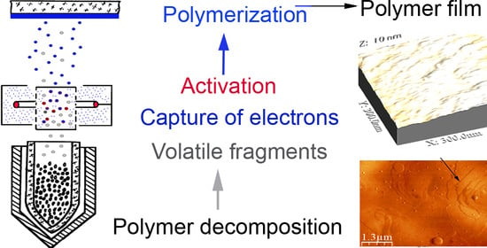
Fluoropolymer thin films have been used as protective coatings, dielectric layers and as a matrix for nanocomposite films [1,2,3,4,5,6,7,8,9]. Recently fluoropolymer (FP) films have been used in organic light emitting diodes [2,3], field effect transistors [4,10] including sublayer for orientation [11], antireflective coatings [12], solar cells [13], hydrophobic coatings [14,15], waveguide [16], as charge storage layer for electricity generator [17]. The deposition methods of the FP films include plasma polymerization of fluorinated compounds; chemical vapor deposition initiated by hot wire (CAT-CVD) from fluorinated monomer; laser, electron, magnetron or ion sputtering of FP target; thermal decomposition and evaporation of the bulk FP in vacuum. The last method was aimed at production of thin film with lowest thermal conductivity and the highest optical absorption. The material had to be isotropic at nanometer level. The material with a combination of these properties is a nanocomposite metal-filled polymer film. The deposition method for polymer should be compatible with existing vacuum equipment and technology for deposition of metals. The method of evaporation-activation of PTFE film deposition in a high vacuum was developed (EVD—Electron activated Vacuum Deposition) [1,7]. The products of the thermal decomposition of the PTFE in a vacuum went through the cloud of accelerated electrons before condensation on a substrate [1,7]. Such the treatment increased deposition rate fivefold and determined the amorphous structure of the PTFE film. The PTFE films were completely transparent in the visible light range and were excellent for application in optics [7].
Thin films of other fluoropolymers like PHFP, polyvinylidene fluoride, Cytop, Teflon AF, and PCTFE were produced in a vacuum [1,2,3,4,5,6,7,8,9,10,11,12,13,14,15,16,17,18,19,20,21]. PHFP films were deposited from a gas phase with plasma polymerization [5,19,20,21], thermal evaporation in a vacuum [19], CAT-CVD [22], and electron-beam polymerization on a surface [23]. PCTFE is a FP with one chlorine atom per unit of macromolecule. Its films were produced by plasma polymerization [24,25,26], electron [18] and laser [27] beam ablation, by thermal evaporation as well [1,7]. The smoothness and optical properties of the fluoropolymer films, deposited by EVD seems high enough for their applications in optoelectronics [1,7,28]. Therefore, all the processes of the FP decomposition, activation of the emitted fragments and film growth mechanism are of scientific interest. Thermal degradation of PTFE was studied with mass-spectroscopy by Luff and White [29] and by Collins [30]. PHFP degradation products contained the same species as from PTFE, but with a different relative concentration [19]. Compared with the evaporated species of PTFE, the PHFP species within the 50–150 amu range are more abundant.
There is a branch of science studying electron-induced reactions in the gas phase of fluorine-containing molecules [31,32,33,34,35]. Dissociative electron attachment to the reactive difluoromethylene molecule CF2, produced in a C3F6 + He plasma was investigated. The upper limit for the cross section of formation of F− via dissociative electron attachment to CF2 was estimated to be 5 × 10⁻⁴ Å2. The authors concluded that difluoromethylene plays a negligible role in negative ion formation. Formation of negative ions was detected at electron energy 7 eV [33]. Electron impact cross sections at energies less than 10 eV were calculated for the CFx (x = 1–3) radical species. The data for CF3I and C2F4 covered cross-sections for electron scattering, electron impact dissociation and dissociative electron attachment [34,35]. Polymerization reactions in RF plasma in CF4, C2F6, and C4F8 gasses were studied by electron attachment mass spectrometry. The density of deposited “polymers” was increased with increasing size of the precursor. In a fluorine-rich environment the deposits were saturated with F(CnF2n+2). As the amount of fluorine in the precursor gas decreased, the degree of F saturation of the deposit also decreased. Wijesundara with coauthors studied the modification of plastic surface with ions CF3+ and C3F5+ with energy 25–100 eV [36]. The structure of deposits resembled the structure of plasma-polymerized fluoropolymer. Concentration maximum of (–CF2–) groups was reached in case of ion energy 50 eV. The authors concluded that polymer was grown more effectively from C3F5+ ions than from CF3+ ions. Our previous studies of gas phase of PTFE [1,7] as well as recent of PHFP and PCTFE evidenced different behavior of each polymer during heating in a high vacuum and during activation by a cloud of electrons.
The aim of this work is to study the whole chain of the fluoropolymer film deposition in vacuum: decomposition-evaporation of the fragments of macromolecules, composition of the gas phase during activation, growth, structure, optical and mechanical properties of the films.
2. Materials and Methods
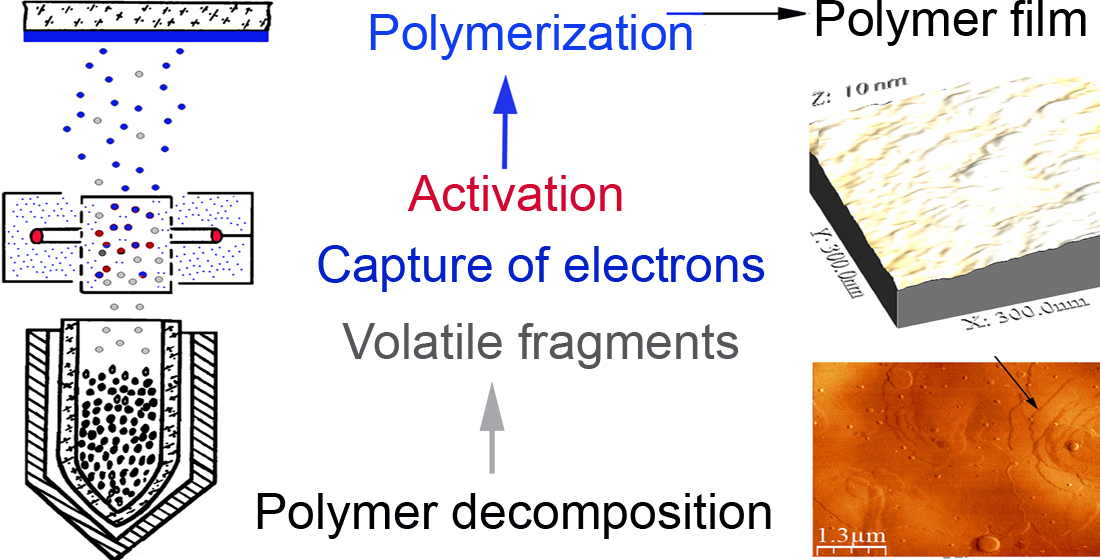
The PTFE, PHFP and PCTFE were purchased from Sigma Aldrich (Darmstadt, Germany). A vacuum set-up UVN-74 with an evaporator for polymer heating and treatment of gases with a cloud of accelerated electrons, as described in [1], was used for depositions. Mass-spectra were recorded with a MX-7301 apparatus (Electron microscopy plant, Sumy, Ukraine) mounted on top of the chamber. The schemes of the evaporator-activators are presented in Figure 1. PCTFE deposition was carried out from a crucible covered with a microporous metal filter. Advanced Energy Caesar 403 (40.68 MHz) was used for plasma generation. More depositions were made in a K. Lesker installation. Mass spectra were recorded using a Prisma apparatus (Pfeiffer vacuum GmbH, Asslar, Germany), mounted on top of the K. Lesker chamber. Starting pressure in the chambers was 10−5 mbar. The deposition rate was controlled by means of a quartz microbalance. The properties of the FPs and deposition conditions are summarized in Table 1.
Films were deposited on polished slides of fused silica, germanium (Ge), silicon (Si), and KBr at an ambient temperature. Some films were detached from a KBr surface, mixed with KBr fine powder and pressed into a pellet. IRS were recorded with a Perkin-Elmer 325, a Specord M80 and a Bomem MB 100 spectrometer. Perkin-Elmer 325 and Specord M80 used films from 5 to 10 micrometers thick on a Ge plate. Bomem MB 100 used films from 50 to 200 nm thick on a Si chip and pellets made from a mixture with KBr powder. Optical spectra were recorded using LAMBDA 1050 UV/Vis/NIR spectrophotometer (PerkinElmer, Inc. Waltham, MA, USA). Refractive indices were measured by ellipsometer SENresearch SE 800 DUV (Sentech Instruments, Berlin-Adlershof, Germany). The morphology of the films was studied with an AFM Nanoscope IIIa Dimension 3000™ at room temperature in a tapping mode. Mechanical properties of the films were measured using Si tip with its apex radius of 30 nm. Hardness of the film was determined as a ratio of maximum loading force to contact area at a given penetration depth. The Young’s modulus was determined using fitting of the initial part of loading curve by Hertz model of elastic contact.
3. Results
3.1. Processes in Gas Phase
During the deposition process the pressure in the chamber was increased to 1–4 × 10⁻⁴ mbar due to emitted fluorocarbon fragments of the FP macrochains. The electron cloud did not increase the film growth rate without accelerating voltage. The deposition rate of both PTFE and PHFP was increased five times immediately after accelerating the voltage was switched on. Their film growth rates were as follows: PTFE—0.5 nm/s with crucible temperature 430 °C and PHFP—0.7 nm/s with crucible temperature 320 °C. The deposition rate of PCTFE was 1.5 nm/s with crucible temperature 420 °C and was independent from electron activation. The PTFE and PHFP did not produce drops during heating. Crucible covered with heated microporous filter was used to prevent inclusion of microdrops in the PCTFE film. The different behavior of FPs during heating in vacuum was due to different combinations of their physical properties, such as the softening temperature and viscosity.
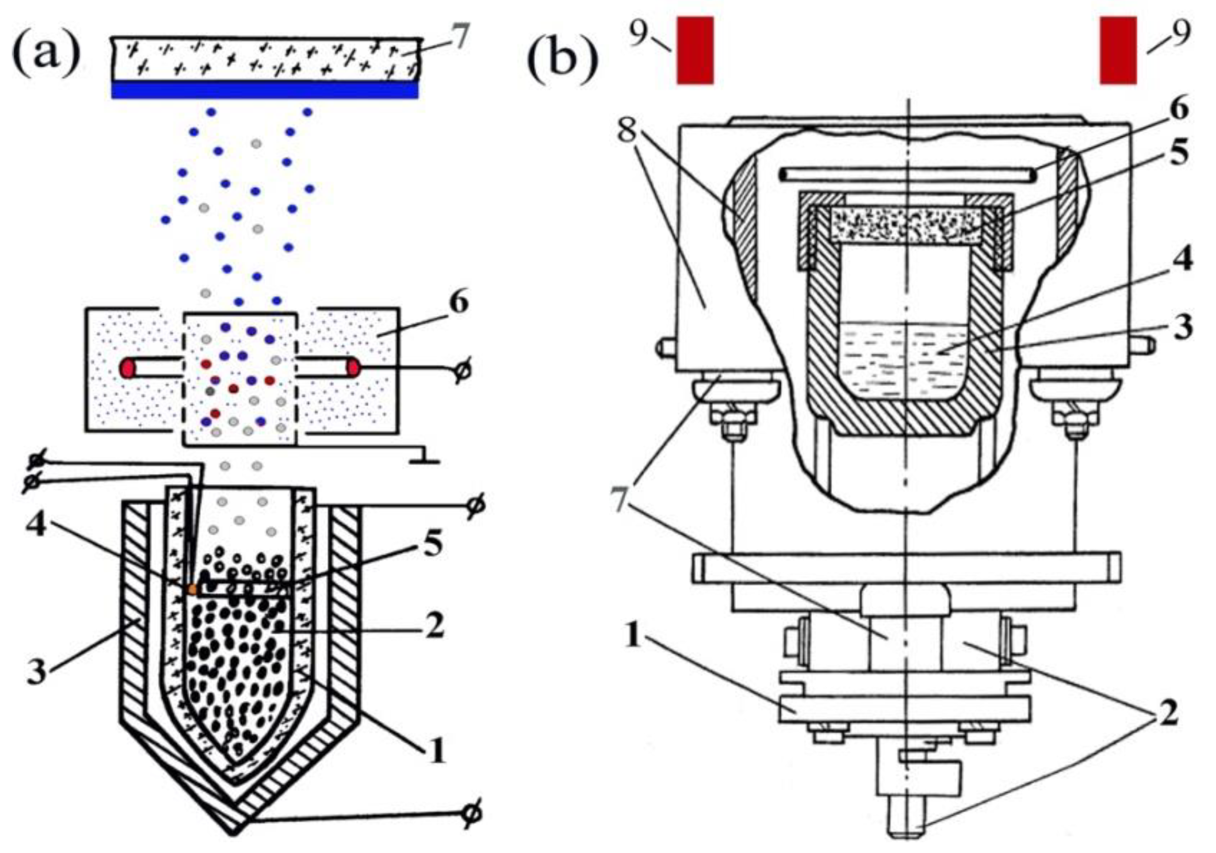
Mass-spectra of the emitted fragments during FPs heating with and without electron activation are shown in Figure 2. The relative concentration of positive ions is presented in Table 2. Relative concentrations of PTFE fragments revealed changes under electron activation. However, activation of fragments that came from a 1 mm hole in a crucible (Q-closed, Table 2) led to other concentrations of the fragments, than from an open crucible. The fragments produced in the first case did not form the film. The concentration of CF3+ and C3F5+ ions was correlated with film deposition rate [1,37]. The data are in a good agreement with those obtained in [36]. The emitted gasses from all the three polymers showed the loss of activity at the pressure corresponding to the mean free path of the fragments [1,7,28]. This is the evidence of the surface polymerization mechanism from comparatively small fragments (30–200 amu) for all three FPs. The presented mass spectrum of the PHFP fragments during heating was the same as was recorded in [19]. During heating of the PHFP the concentration of CF3+ and C3F5+ ions was more abundant, than the same species emitted during decomposition of PTFE. The PHFP fragments under treatment of the electron cloud showed changes in ion concentration, unlike the changes of the PTFE fragments. The concentration of CF3+ was increased but the concentration of the C3F5+ ions was decreased. The mass spectrum of the PCTFE fragments which went through a heated porous filter showed the peaks assigned to fragments with and without chlorine.
Mass-spectra which were recorded during PTFE deposition with activation by accelerated electrons with various voltage and constant film deposition rate 2 nm/s in extended mass range are shown in Figure 3. With slight variations, all the mass-spectra revealed the same behavior under electron activation. The quantity of fragments with a molecular mass higher than 131 amu was small. Taking into account that the usage of evaporated material in the film was calculated up to 50% [7], we concluded that the FP film was grown from small fragments, but not from large ones as it was stated in [18].
3.2. Structure of the Films by Infrared Spectroscopy
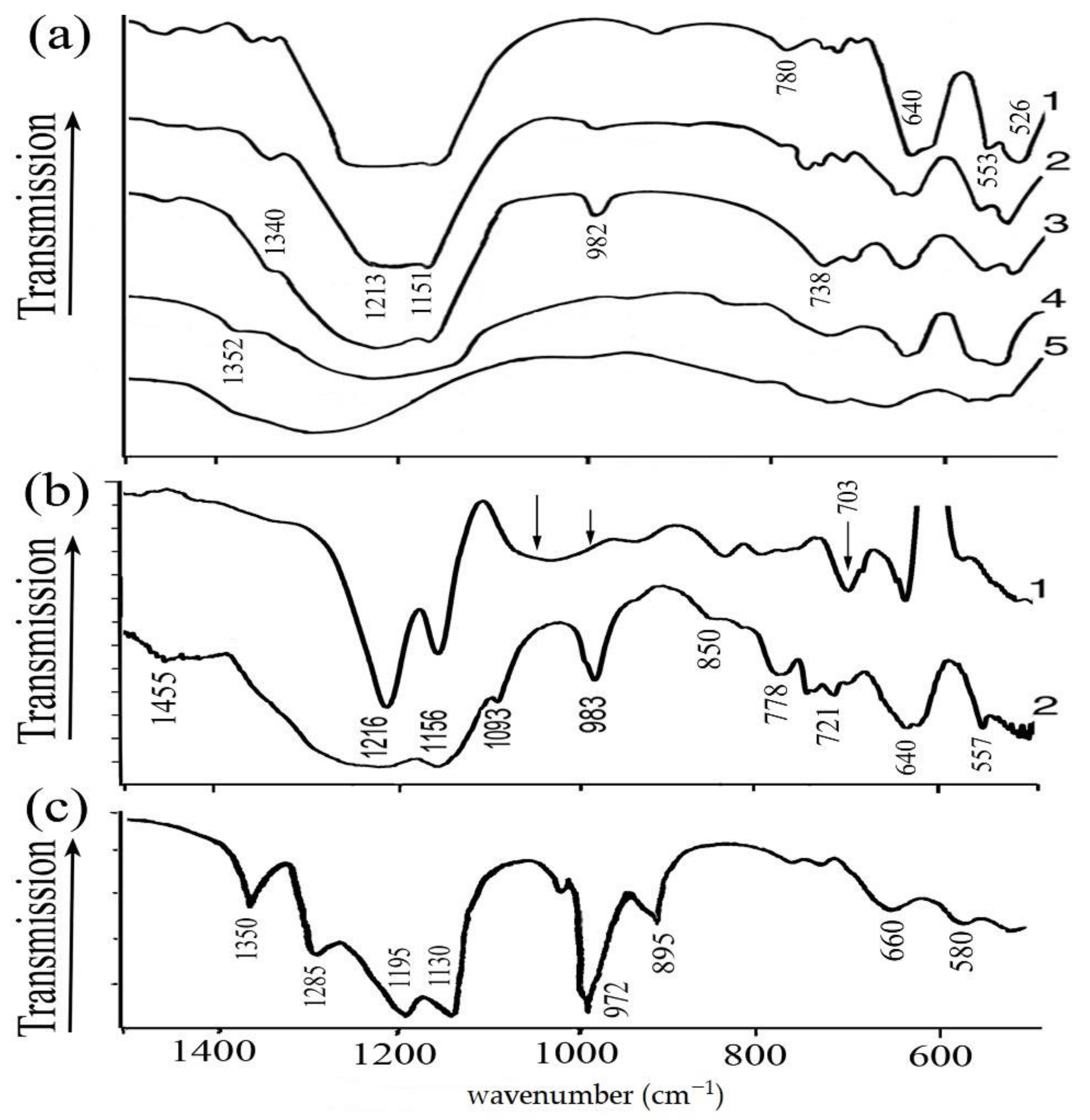
The IRS of PTFE films produced by EVD are depicted in Figure 4a. All IRS bands and assignation of the bands are presented in Table 3. The IRS of the PTFE films resembled the IRS of bulk PTFE [38,39,40] and were described in [1,7,28]. Two spectra are of the films deposited by EVD with RF discharge. The bands located nearby 526, 555, 640, 729, 1151, 1213 cm−1 were attributed to 157 PTFE conformation. The band 980 cm−1 was assigned to –CF3 groups [41,42], the band 1352 cm−1—to –C=C– groups [1,7,41]. The assignation of the band 1352 cm−1 to methylene group seems less probable due to high vacuum conditions. An increase in the electron activation current led to an increase in the relative intensity of bands 980 cm−1 and 1352 cm−1, therefore, the concentration of these groups was increased. The bands 703 and 738 cm−1 were assigned to an amorphous phase [38,41]. The electron activation of the gaseous fragments made the film amorphous. The films produced by EVD of PTFE consist of the polymer macromolecules (repeated –CF2–) of an unknown chain length with a small quantity of the chain units with a double bond or side branch. The low power RF discharge during EVD led to 1352 cm−1 band intensity growth, showing an increase in the concentration of –C=C– groups. The band 980 cm−1 seemed to disappear, but absorption at this frequency was not equal to zero. This can be explained by attachment of the –CF3 in an atactic manner. The increase of RF power led to the growth of absorption of 1352 cm−1 band, it became wide indicating significant cross-linking. The concentration of –CF2– groups was decreased and became comparable with the concentration of –C=C– groups. The films deposited by EVD with high RF power had a structure like films deposited in classic plasma: a lower quantity of repeated –CF2– units and higher quantity of double bonds and cross-links as compared with bulk PTFE. The band 640 cm−1 of medium intensity shows that some chains were oriented perpendicular to a substrate surface [43]. The IR signal in the 1480–2000 cm−1 diapason for the EVD PTFE film was on a noise level, indicating a very small quantity of the side groups with a double bond, in particular, oxygen-containing. The weak bands 2336 and 2361 cm−1 appeared in the IRS of the EVD PTFE film. They were assigned to a combination of bands of two modes associated with –CF2– stretching [38].
IRS of the PHFP film on Si chip and of the pilled PHFP pressed with KBr powder are shown in Figure 3. All bands of these IRS are close to bands of IRS of the bulk polymer [44]. The narrow IRS bands indicated a linear structure of the PHFP macromolecules with small quantity of cross-links. The bands located at 1216 and 1156 cm−1 were attributed to –CF2– stretching vibrations; 640, 557 and 509 cm−1 were attributed to chain stretching and –CF2– bending, respectively. The band about 1455 cm−1 can be attributed to C=C bonds or other defects of PHFP chain. The intense band at 983 cm−1 indicated higher concentration of –CF3 groups in the PHFP film, than in the PTFE films. Therefore, the film structure is closer to the pristine PHFP, than to the PTFE. The comparison of the IRS of pilled material and film on Si showed important information about material structure. The differences in shape and intensity of the band around 983 cm−1 indicated a not isotropic position of the –CF3 groups in the film as relative to the Si surface. The wide shape of this band for the film IRS showed that –CF3 groups were attached to the main chain in an atactic manner. An intense band at 703 cm−1 coincided with the same band in IRS of bulk PHFP. The comparison of these IRS with IRS of the plasma and electron beam polymerized films [20,21,22,23,24] showed higher relative intensity of the band of -CF3 groups in the EVD PHFP film.
The IRS of the PCTFE film was more similar to the spectrum of bulk PCTFE, than to oligomers of PCTFE [40,45]. Bands 506, 580, 1130, 1195 cm−1 were attributed to –CF2– vibrations of PCTFE macromolecule. Bands 1285 and 1350 cm−1 were attributed to vibrations of –CF– and –C=C–CF. Intense bands 895 and 972 cm−1 were attributed to –C–Cl stretching vibrations. Weak bands at 725 and 755 cm−1 coincided with bands of bulk PCTFE. Band 660 cm−1 was attributed to C–C skeletal stretching. The bands of the film IRS were relatively sharp, indicating a linear structure of the macromolecules.

Table 3.
Bands of IRS and their possible interpretation.
| Frequency, cm−1 | Vibration | Band Intensity, PTFE | Band Intensity, PHFP PCTFE | Reference | |||
|---|---|---|---|---|---|---|---|
| Thermal | EVD | EVD+RF | EVD | Thermal | |||
| 509 | CF2 bending | w | w | w | m | m | [40] |
| 526 | CF2 bending | m | m | m | m | w | [40] |
| 553/557 | CF2 deformation | m | m | m | m | w | [40] |
| 580 | CF2 wagging | - | - | - | - | w | [40] |
| 620 | CF2 wagging | m | m | m | m | - | [38] |
| 640/660 | Chain stretching | m | m | m | m | m | [40] |
| 703 | Amorphous | w | w | w | m | w | [38,41] |
| 721 | Amorphous | w | w | w | m | w | [38] |
| 738 | Amorphous | w | m | m | m | w | [38,41] |
| 780/778 | CF2 | w | w | w | m | w | [41] |
| 850 | Amorphous | - | - | - | w | - | [38] |
| 895 | CCl stretching | - | - | - | - | m | [45] |
| 972 | CCl stretching | - | - | - | - | s | [40] |
| 982/983 | CF3 | - | w | w | s | - | [42] |
| 1151/1156/1139 | CF2 sym stretch. | s | s | s | s | s | [40] |
| 1213/1216/1195 | CF2 asym stretch. | s | s | s | s | s | [40] |
| 1285 | CF stretching | - | - | - | - | m | [40] |
| 1340 | –C=CF2 | w | m | m | w | - | [18] |
| 1352/1350 | –C=C- | w | w | m | w | m | [18,42] |
| 1455 | CF2 sym stretch. | w | w | w | w | - | [40] |
w—weak, m—medium, s—strong intensity; -/-/- means PTFE/PHFP/PCTFE frequencies.
3.3. AFM Studies of the Films Surface and Mechanical Properties
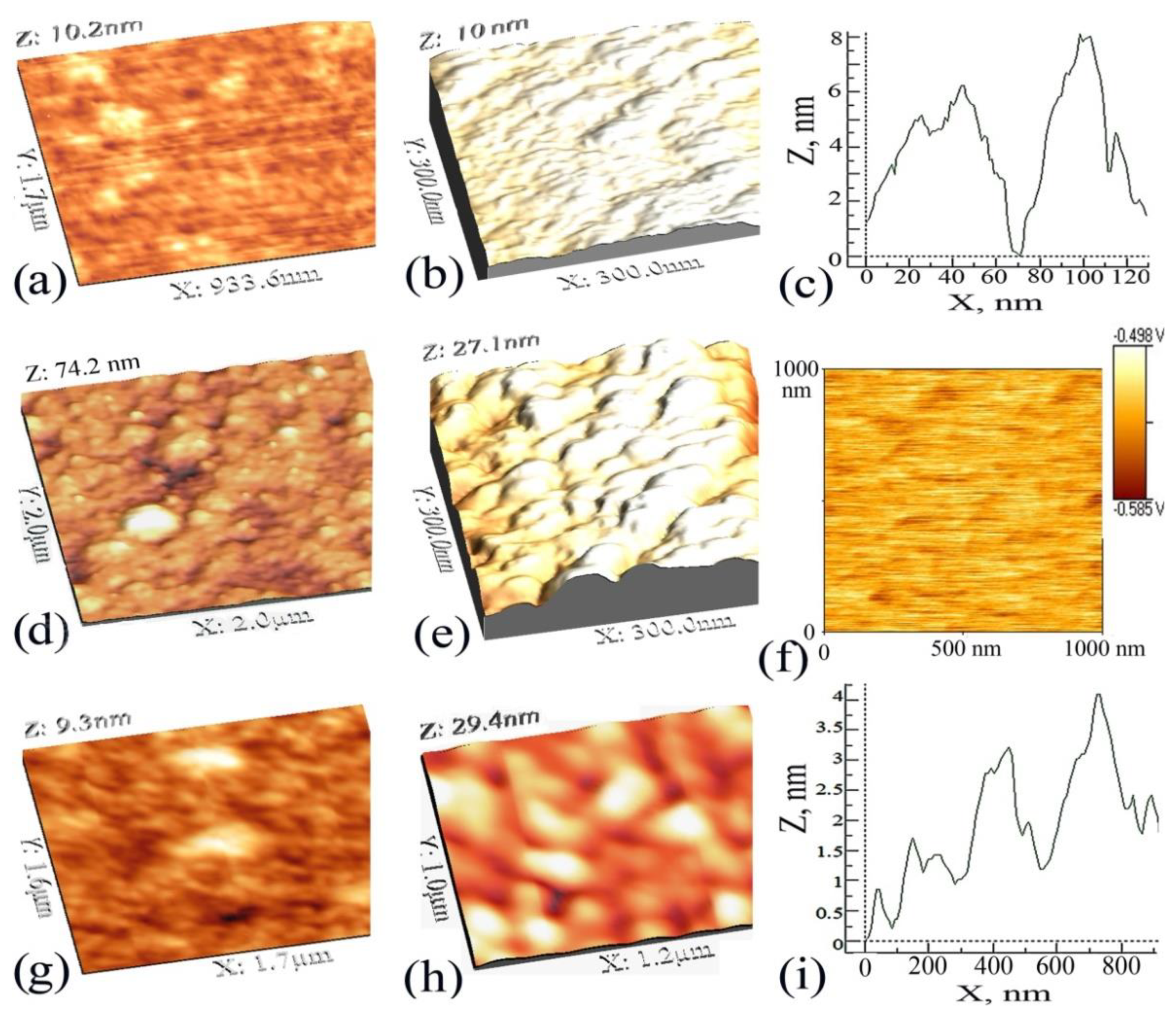
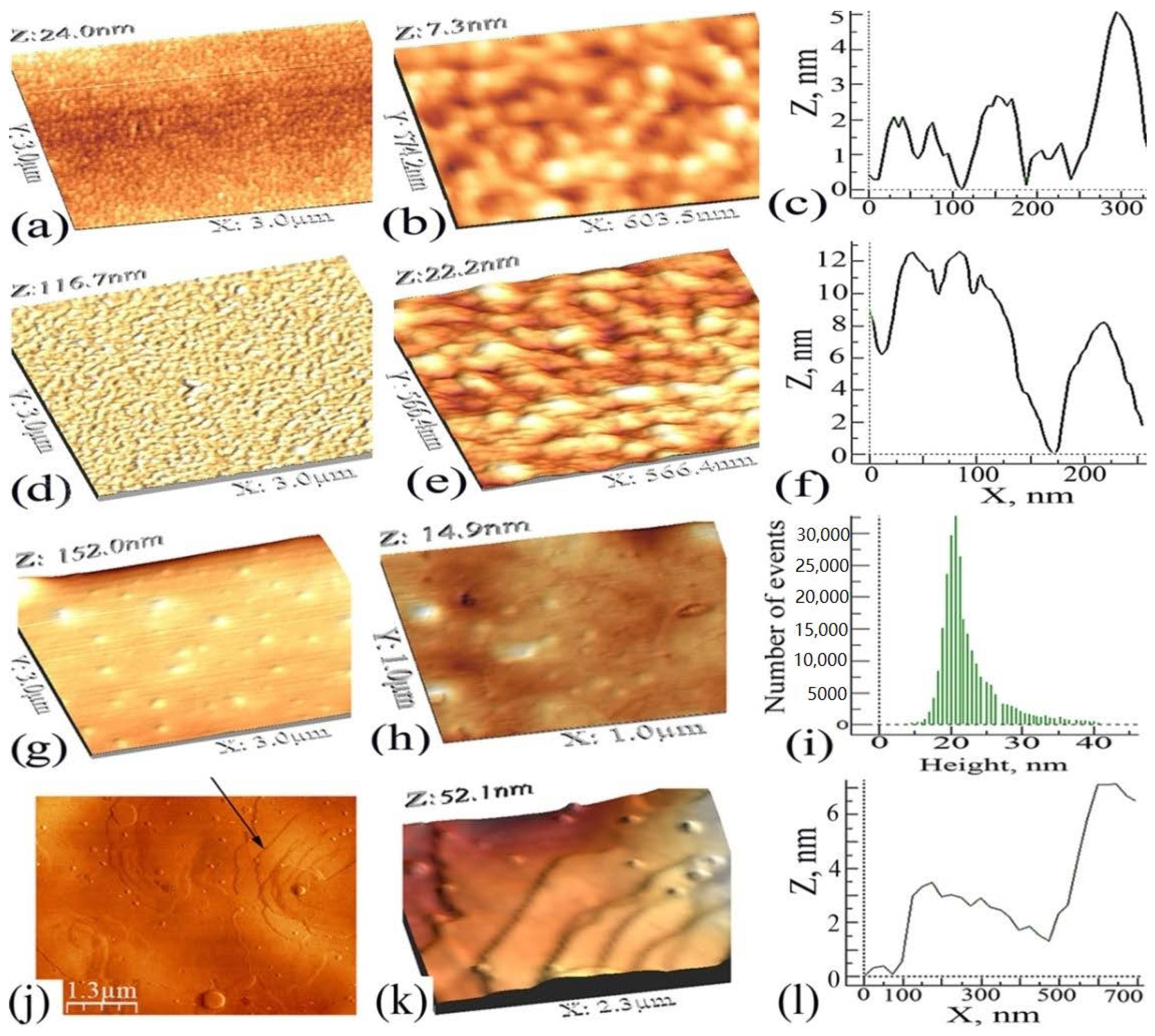
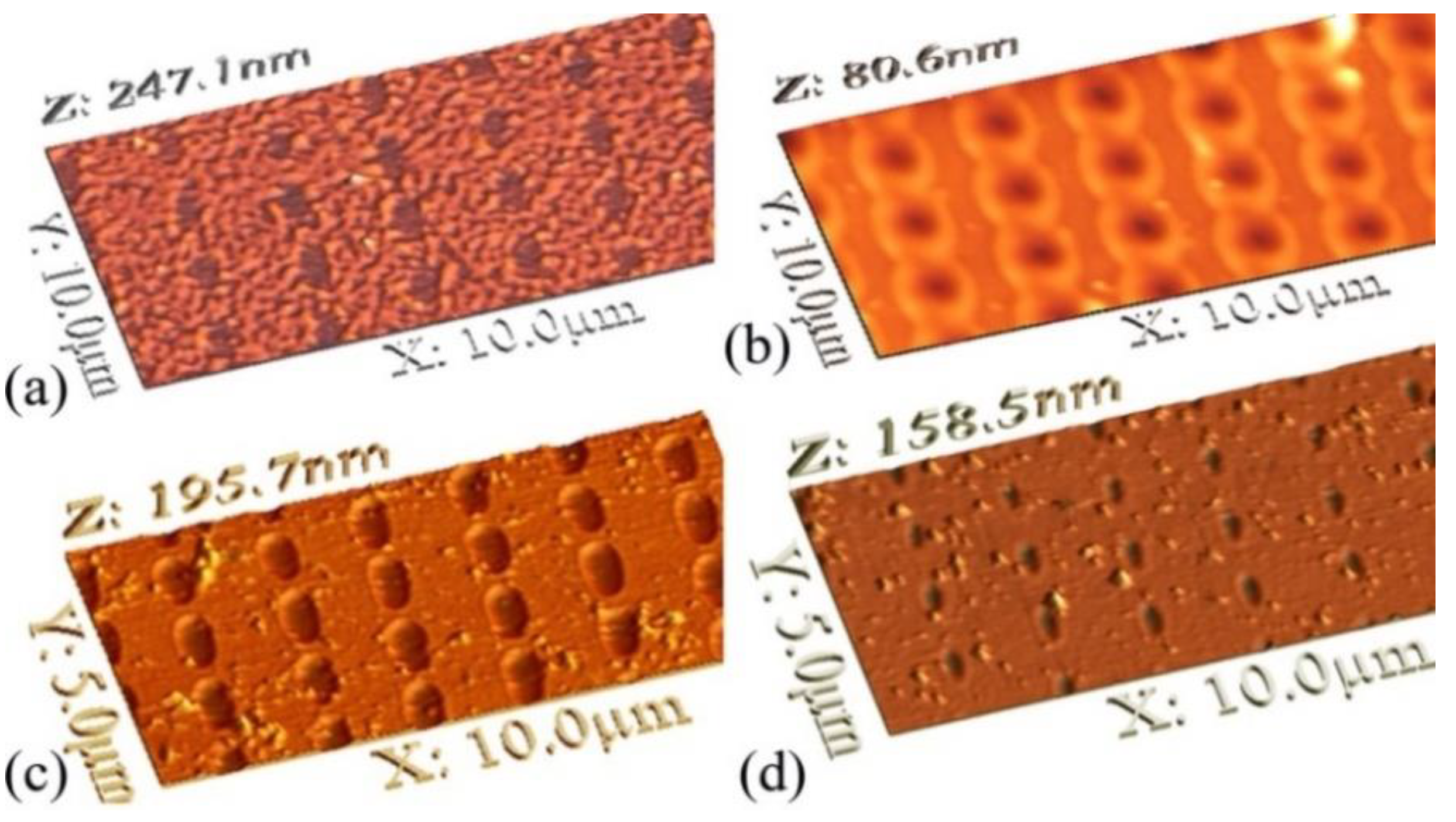
AFM images of FP films are presented in Figure 5 and Figure 6. The surface of the EVD PTFE thin film represents bumps with length of about 70 nm with a roughness of about 8 nm. The thicker the PTFE film the bigger the surface roughness. Pressure elevation increased the film roughness due to formation of polymer drops in the gas phase, which were condensed on the substrate. The formation of the observed surfaces (Figure 5b,c,e) was the result of Volmer–Weber growth mechanism. A negative electric charge was detected in the PTFE films. RF plasma during EVD at low pressure slightly decreased the surface roughness (Figure 5g,h). The surface roughness of the PHFP films was increasing with film thickness (Figure 6a–f). These surfaces seemed to be formed with “islands” up to 500 nm in size, which, in turn, are composed from smaller units of 30–100 nm. Perhaps, this was the result of the coalescence of primary polymer clusters formed with Volmer–Weber mechanism. The surface relief of the PCTFE films was dependent on the deposition conditions and film thickness (Figure 6g–l). Microdrops appeared during nonoptimal deposition conditions. The PCTFE films have a layered structure with layer thickness of about 4–8 nm, indicating Frank-van der Merwe growth mechanism. The numerous nuclei on film surfaces are the evidence of this mechanism.
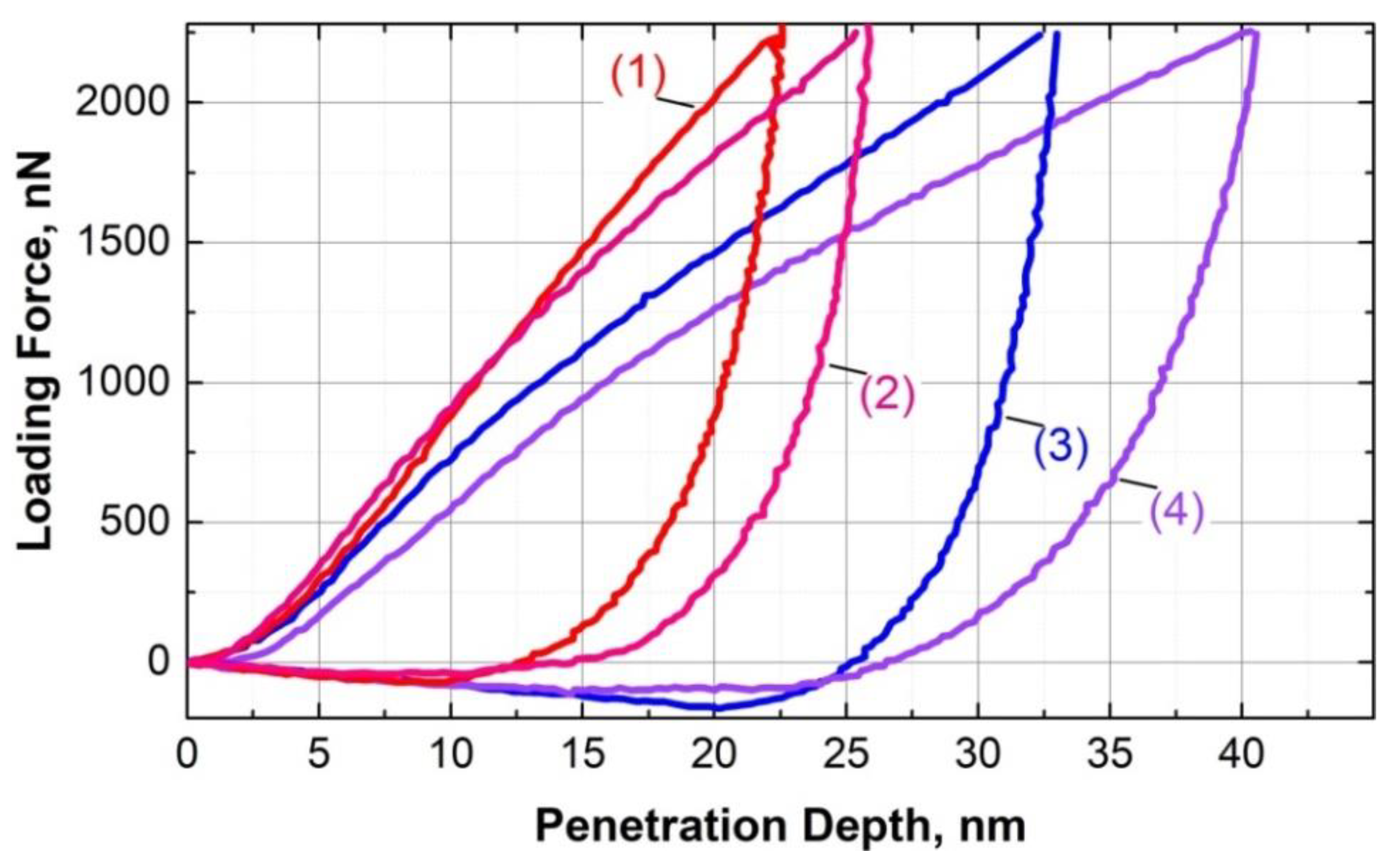
Deposition conditions had a significant effect on the mechanical properties of the FP films. Figure 7 shows the influence of deposition conditions on mechanical properties of the PTFE films. The Young’s modulus for EVD PTFE film deposited with high rate was 3.09 GPa, for EVD PTFE film deposited with small rate was 3.26 GPa. The EVD+RF provided a film with smaller penetration depth and a larger segment of elastic deformation in the loading curve compared to the EVD. EVD+RF plasma increased the Young’s modulus of the PTFE film to 4.55 GPa. Even if only upper half of the film was deposited by EVD+RF, the Young’s modulus was 4.15 GPa. The mechanical properties of the PTFE films deposited with EVD and EVD+RF plasma are comparable with the properties of the best FP films produced by classic plasma methods [46].
3.4. Optical Properties of the Films
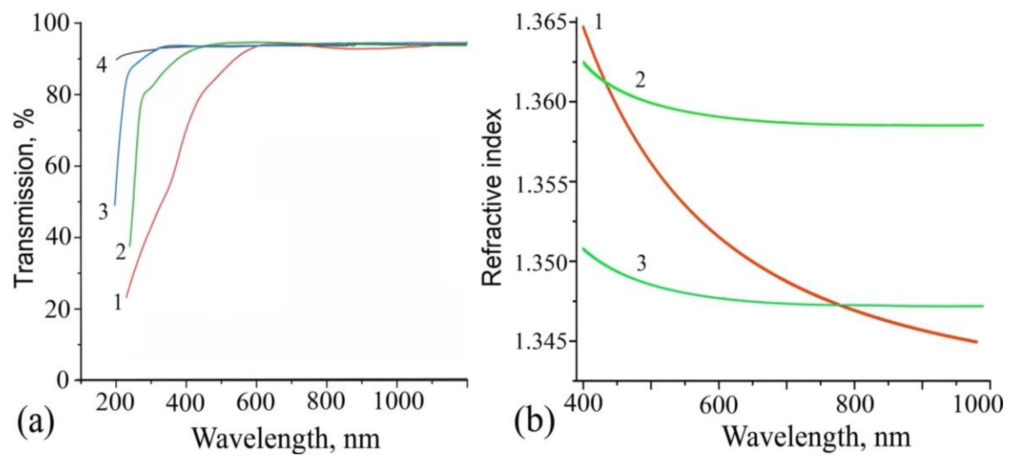
All FP thin films were transparent from the ultraviolet via the visible to the near-infrared region. Optical transmission spectra and refractive index of the FP films are shown in Figure 8. They are close to optical properties of standard fluoropolymer films [47]. The PCTFE film was the most transparent one. The smaller transmission of the PHFP film in ultraviolet region compared to the other films and precursor polymer can be due to a nano-island structure of the film. The refractive index of the PHFP deposits was the same for the films of 50, 100 and 200 nm thicknesses, indicating no changes in film structure with its thickness increase. The thicker PTFE film had higher refractive index. This gives evidence for a more dense structure of the thicker film. The PTFE film deposited by EVD+RF at low RF power had the same transmission spectrum.
3.5. Dye-Filled PTFE Films
Using the EVD method, polymer films filled with molecules of various dyes were produced by codeposition [27,28]. The polymethine, squaraine, cyanine, phthalocyanine, spiropyran, and styryl dyes were introduced into the PTFE matrix at various concentrations. Dye molecules in the PTFE matrix revealed an extreme stability towards actions of all external factors: irradiation by light, heating in air, immersion in aggressive gasses and liquids [48,49,50]. PTFE film filled with 25% of nullmethinmerocyanine dye was used for thermolitography [51,52]. Figure 9 presents submicron marks made by focused laser beam (405 nm) in dye-filled polymer films.
Figure 9a shows damage of the film after irradiation due to the close melting temperature of a dye-filler and a thermoplastic polymer matrix. Figure 9b shows an extended outflow in the irradiated zone of more a thermal stable molten thermoplastic polymer. Adjusting the optimal ratio between the thermophysical properties of the polymer matrix and dye-filler, the thermolitography process was tuned. Due to an extremely high viscosity at high temperatures the film with PTFE matrix had no liquid outflow (Figure 9c,d). This is necessary for the high-density optical recording of information and thermolitography with high resolution.
4. Discussion
During the EVD which takes place in a comparatively high vacuum, on average only one collision between fragments is possible on their way towards the substrate or no collision at all. Electrons without acceleration voltage failed to activate fragments in the gas phase. Activation with accelerated electrons led to an elevation of the growth rate of PTFE and PHFP films by factor of up to five. Activation led to an increase of relative concentrations of CF3+ and C3F5+ and decrease of CF+ and C2F4+ fragments during PTFE decomposition. Taking into account the small electron energy necessary for CxFy fragment ionization [33,34,35,36], the main contribution to fragment activation was caused by scattered secondary electrons. In the PHFP the main chain carries CF3 side groups, which lead to different physical constants of the polymer such as melting temperature and decomposition rate vs. temperature. It appears that the PHFP chain tends to decompose into larger fragments. The existence of CF3+ and C3F5+ fragments was necessary, but was not sufficient for the film formation. For the investigated polymers, film formation is assumed to follow a polymerization process which could be radical, ionic or both. The effect of the magnetic field on the morphology of the PTFE film was revealed [53]. A negative electric charge was found in the PTFE films. These data showed the capture of the electrons by gaseous fragments. Therefore, the growth of perfluoropolymer film might include negatively charged fragments, or at least their participation plays a major role in the polymerization process. No increase of the PCTFE film growth rate was observed under electron activation indicating another mechanism of polymerization.
The IRS showed that all the fluoropolymer films were composed of linear polymer chains with small concentration of cross-links. No side groups of inclusions were detected at the level of the IRS sensitivity. The macromolecules in the EVD films can have shorter chain length than macromolecules in bulk FP. The additional low power RF plasma can increase the chain length and cross-links quantity. EVD and plasma action on gaseous molecules led to the formation of fragments sometimes with three reactive bonds. Such fragments during film growth formed groups with either double bonds, side groups or cross-links, but not in a systematic repeated way. Such units with no repeated structure have no fixed frequency, so widened and very weak bands cannot be recorded, if the concentration of the defective groups was small. The structure of EVD and EVD+RF films can be suggested as linear chains in some rare sites cross-linked one to the other. The very high hardness and Young modulus can be explained by partial crosslinking of the FP. However, the crystallization of EVD PTFE film during heating supports the very small quantity of the cross-links in it [1,7]. EVD+RF film was not crystallized, revealing more crosslinks. However, EVD+RF film was certainly not like material collected from different fragments in a nonrepetitive manner. It should be mentioned that the assignation of IR bands in reference literature is still not unequivocal. Further research into the fine details of PTFE film structure deposited by EVD+RF using the IRS combined with other structural-sensitive methods can produce new interesting results.
The AFM studies of the film morphology showed that the Volmer–Weber mechanism can be responsible for perfluoropolymer film growth, whilst the formation of the PCTFE film was due to the Frank-van der Merwe mechanism. The observed differences in the surface relief and the growth mechanisms can be due to significantly different physical properties of the FP, such as the softening temperature and viscosity (Table 1). This difference reflects various ratios between inter- and intramolecular interactions in the FP and their interaction with the substrate.
The values of the refractive indices for the deposited FP films are higher than for the films deposited by CAT-CVD from hexafluoropropylene oxide [22]. The smaller refractive index of CAT-CVD films indicates a presence of air in the films. The authors of [54] obtained thin films of Teflon FEP with a somewhat higher refractive index than that of the sputtered target material. This increased value of the refractive index could be caused by dense packing in the film or by inclusion into the film of impurities such as carbonized clusters and other chemical groups synthesized in the plasma at a comparatively high pressure. Refractive index of films deposited with a low power classic plasma in CHF3 gas was 1.39 [55]. However, absorption of the film in the blue region was higher than for the films produced by EVD. These data suggest that the plasma film structure was densely packed but with a fluorine deficit.
Surface topography of a film is determined by competition between processes leading the material to an equilibrium state and processes keeping the material in a nonequilibrium state. The equilibrium state is characterized by the supramolecular organization of the polymer. The morphology formation and other properties of the film is a result of multiparametric system of polymer properties and deposition conditions. Porosity, surface relief and refractive index of films can be controlled by a variation in pressure and electron activation power. EVD+RF plasma allows control of crosslinking almost independently from pressure and deposition rate. The RF plasma at a low pressure with previously injected charge carriers produces fluorine-deficient fragments in a gas phase only, avoiding gas phase coupling and damage of the growing polymer chains on a substrate. These are the main differences between EVD+RF and classic RF discharge at a higher pressure. The discussion concerning these differences is presented in the Supplementary Material. Films with a rough surface can be produced at high pressures and can be useful for superhydrophobic coatings.
Dye-filled PTFE films were obtained for the first time, combining EVD for PTFE and thermal heating for dyes. The outstanding properties of dye-filled PTFE films cannot be explained by the sum of the properties of the components. The origin of the extreme stability of dye molecules in PTFE matrix should be studied further.
In general, the deposition of FP thin films as studied here exploits the decomposition of polymers under a high vacuum. The main difference to other methods consists in the use of activation of emitted fragments by a cloud of accelerated electrons. The 10−5 mbar pressure of residue gasses in the chamber is proof of the high purity of deposited FP films. Combining different FP in multilayered systems or varying their refractive index by deposition conditions, complex optical devices can be produced. To further clarify the activation and growth mechanisms of FP films, an investigation involving mass-spectrometry of both positive and negative ions is required together with advanced studies of processes on the substrate surface like described in [56]. The necessity of charged fragments for FP film growth during EVD should be studied in detail as they are important for plasma film deposition [57].
5. Conclusions
Thin films of three fluoropolymers with surface smoothness at nanoscale were produced by decomposition-evaporation of bulk fluoropolymers in a vacuum. Electron activation of the emitted fragments was necessary for PTFE and PHFP film growth. PCTFE films were deposited by thermal decomposition. Differences in the concentration of the same emitted fragments in the PTFE and PHFP mass-spectra were identified. They can be caused by the presence of a side CF3 group in the PHFP macromolecule. The negative charge in the PTFE film points to the electrons attachment to condensed fragments. The decomposition, activation and growth mechanisms of perfluoropolymers were different from those of PCTFE. The films of all fluoropolymers were grown from small fragments of polymer chains. The deposited fluoropolymer films were composed from mainly linear macromolecules with a small quantity of crosslinks, instead of highly crosslinked plasma “polymers”. The combination of EVD and RF plasma produced films with the advantages of both plasma polymerized and EVD films, but without limitations imposed by classic plasma. The optical properties of thin films of fluoropolymers make them promising candidates for applications in optoelectronic and photonic devices. Dye-filled PTFE films were produced for the first time by the codeposition of dye and PTFE. The films of this new nanocomposite material revealed an excellent stability of the optical properties of the dye-fillers of various types to the actions of all external factors. The next advance is planned by application of polymerizable dyes for codeposition with fluoropolymers.
Supplementary Materials
The following are available online at https://0-www-mdpi-com.brum.beds.ac.uk/2571-9637/4/1/9/s1, A comparison of backgrounds of plasma discharge in organic gas and EVD.
Author Contributions
Concept: S.S. and K.G.; deposition methodic and depositions: K.G., Y.K., V.K.; mass-spectrometry: K.G. and V.K.; AFM measurements: P.L., AFM data processing: P.L. and K.G.; optical and IRS measurements: V.K and B.D.; writing: all authors wrote the parts that concerned their experiments; Manuscript: K.G.; editing: S.S.; administration: in Germany S.S. and B.D., in Ukraine K.G.; Funding acquisition: S.S. and K.G. All authors have read and agreed to the published version of the manuscript.
Funding
German Ministry of Education and Research, the contract no. 03WKP50A. Additionally funded by National Academy of Sciences of Ukraine. DAAD funded the stay of K. Grytsenko at TH Wildau, Grant no. 91697212.
Acknowledgments
Thanks go to Claus Villringer (D) for the ellipsometric measurements and to Anastasia Gritsenko (UK) for English editing.
Conflicts of Interest
The authors declare no conflict of interest.
References
- Gritsenko, K.P.; Krasovsky, A.M. Thin film deposition of polymers by vacuum degradation. Chem. Rev. 2003, 103, 3607–3650. [Google Scholar] [CrossRef]
- Yaschchuk, V.M.; Gytsenko, K.P.; Schrader, S.; Navozenko, O. Applications of vacuum deposited perfluoropolymer films in OLED and OFET. Bull. Kyiv Univ. 2017, 2, 109–118. [Google Scholar]
- Shin, J.Y.; Kim, T.W.; Kim, G.Y.; Lee, S.M.; Hong, J.W. Performance of three-layered organic light-emitting diodes using the hole-transport and injection layer of TPD and Teflon-AF, and the electron-injection layer of Li2CO3 and LiF. Trans. Electr. Electron. Mater. 2017, 18, 89–92. [Google Scholar] [CrossRef] [Green Version]
- Roh, J.; Cho, I.-T.; Shin, H.; Baek, G.W.; Hong, B.H.; Lee, J.-H.; Jin, S.H.; Lee, C. Fluorinated CYTOP passivation effects on the electrical reliability of multilayer MoS2 field effect transistors. Nanotechnology 2015, 26, 455201. [Google Scholar] [CrossRef]
- Ruckenstein, E.; Gourisankar, S.V. Preparation and characterisarion of thin film surface coatings for biological environments. Biomaterials 1986, 7, 403–422. [Google Scholar] [CrossRef]
- Grytsenko, K.P.; Kolomsarov, Y.V.; Belyaev, O.E.; Schrader, S. Protective applications of vacuum deposited perfluoropolymer films. Semicond. Phys. Quantum Electron. Optoelectron. 2016, 19, 139–148. [Google Scholar] [CrossRef] [Green Version]
- Grytsenko, K.P. Design and Research of Thin Film Metal-Polymer Materials for Optical Information Carrier of Computer. Ph.D. Thesis, Metal-Polymer Research Institute of National Academy of Sciences of Belarus, Gomel, Belarus, 1997. [Google Scholar]
- Gritsenko, K.P.; Capobianchi, A.; Convertino, A.; Friedrich, J.; Schulze, R.D.; Ksensov, V.; Schrader, S. Polymer-Metal Composite Thin Film Prepared by Co-Evaporation in Vacuum. In Polymer Surface Modification and Polymer Coatings by Dry Process Technologies; Iwamori, S., Ed.; Research Signpost: Kerala, India, 2005; pp. 85–109. [Google Scholar]
- Takele, H.; Kulkarni, A.; Jebril, S.; Chakravadhanula, V.S.K.; Hanisch, C.; Strunskus, T.; Zaporojtchenko, V.; Faupel, F. Plasmonic properties of vapour-deposited polymer composites containing Ag nanoparticles and their changes upon annealing. J. Phys. D Appl. Phys. 2008, 41, 125409. [Google Scholar] [CrossRef]
- Shokouh, S.H.; Jeon, P.J.; Pezeshki, A.; Choi, K.; Lee, H.S.; Kim, J.S.; Park, E.Y.; Im, S. High-performance, air-stable, top-gate, p-channel WSe2 field-effect transistor with fluoropolymer buffer layer. Adv. Func. Mater. 2015, 25, 7208–7214. [Google Scholar] [CrossRef]
- Pandey, S.S.; Pandey, M.; Nagamatsu, S.; Kumari, N. Recent advances in orientation of conjugated polymers for organic field-effect transistors. J. Mater. Chem. C 2019, 7, 13323–13351. [Google Scholar] [CrossRef]
- Wang, B.; Ruud, C.J.; Price, J.S.; Kim, H.; Giebink, N.C. Graded-index fluoropolymer antireflection coatings for invisible plastic optics. Nano Lett. 2019, 19, 787–792. [Google Scholar] [CrossRef]
- Zhang, P.; Xu, X.; Dang, Y.; Huang, S.; Chen, X.; Kang, B.; Silva, S.R.P. PTFE/MoO3 Anode bi-layer buffer layers for improved performance in PCDTBT:PC71BM blend organic solar cells. ACS Sustain. Chem. Eng. 2016, 4, 6473–6479. [Google Scholar] [CrossRef]
- Psarski, M.; Pawlak, D.; Grobelny, J.; Celichowski, G. Hydrophobic and superhydrophobic surfaces fabricated by plasma polymerization of perfluorohexane, perfluoro(2-methylpent-2-ene), and perfluoro(4-methylpent-2-ene). J. Adhes. Sci. Technol. 2015, 29, 2035–2048. [Google Scholar] [CrossRef]
- Yi, N.; Baj, S.; Zhou, H.; Xin, Y.; Huang, A.; Ma, Y.; Li, R.; Jin, P. Preparation of microstructure-controllable superhydrophobic polytetrafluoroethylene porous thin film by vacuum thermal evaporation. Front. Mater. Sci. 2016, 10, 320–327. [Google Scholar] [CrossRef]
- Karre, V. Direct Electron Patterning of Teflon-AF and Its Application to Optical Waveguides. Master’s Thesis, University of Kentucky, Lexington, KY, USA, 2009. [Google Scholar]
- Xu, W.; Zheng, H.; Liu, Y.; Zhou, X.; Zhang, C.; Song, Y.; Deng, X.; Leung, M.; Yang, Z.; Xu, R.X.; et al. A droplet-based electricity generator with high instantaneous power density. Nature 2020, 578, 392–396. [Google Scholar] [CrossRef]
- Zadorozhny, V.G. Physical-Chemical Processes During Polymer Deposition in Vacuum and Creation of the New Technologies. Ph.D. Thesis, Institute of High Molecular Compounds of National Academy of Sciences of Ukraine, Kyiv, Ukraine, 1989. (In Russian). [Google Scholar]
- Murakami, Y.; Shintani, T. Vacuum deposition of teflon-FEP. Thin Solid Films 1972, 9, 301–304. [Google Scholar] [CrossRef]
- Chen, R.; Gorelik, V.; Silverstain, M.S. Plasma polymerization of hexafluoropropylene: Film deposition and structure. J. Appl. Polym. Sci. 1995, 56, 615–623. [Google Scholar] [CrossRef]
- Garrison, M.D.; Luginbühl, R.; Overney, R.M.; Ratner, B.D. Glow discharge plasma deposited hexafuoropropylene films: Surface chemistry and interfacial materials properties. Thin Solid Films 1999, 352, 13–21. [Google Scholar] [CrossRef]
- Lau, K.K.S.; Caulfield, J.A.; Gleason, K.K. Variable angle spectroscopic ellipsometry of fluorocarbon films from hot filament chemical vapor deposition. J. Vac. Sci. Technol. A Vac. Surf. Films 2000, 18, 2404–2411. [Google Scholar] [CrossRef]
- Bruk, A.; Zhikharev, E.N.; Volegova, I.A.; Spirin, A.V.; Kozlova, N.V.; Teleshov, E.N.; Kal’nov, V.A. The mechanism of formation and some properties of thin fluorocarbon films deposited onto silicon plates by electron beam polymerization of hexafluoropropylene from the vapor phase. Polym. Sci. Ser. B 2010, 52, 81–85. [Google Scholar] [CrossRef] [Green Version]
- Hallahan, J.R.; Wydeven, T.; Johnson, C.C. Combination moisture resistant and antireflection plasma polymerized thin films for optical coatings. Appl. Opt. 1974, 13, 1844–1849. [Google Scholar] [CrossRef]
- Martinu, L. Deposition and structure of gold containing plasma polymerized halocarbon films. Thin Solid Films 1986, 140, 307–319. [Google Scholar] [CrossRef]
- Tsuji, O.; Minaguchi, T.; Nakano, H.; Tatsuta, T. Surface using property of plasma deposited copolymer films chlorofluorocarbon with ethylene monomer. J. Photopolym. Sci. Technol. 1997, 10, 143–148. [Google Scholar] [CrossRef] [Green Version]
- Grytsenko, K.P.; Schrader, S. Nanoclusters in polymer matrices prepared by co-deposition from a gas phase. Adv. Colloid Interface Sci. 2005, 116, 263–276. [Google Scholar] [CrossRef]
- Grytsenko, K.P. Vacuum-evaporation deposited polytetrafluoroethylene films: Growth mechanism, properties and applications of vacuum-deposited PTFE films. Russ. J. Gen. Chem. 2009, 79, 642–656. [Google Scholar] [CrossRef]
- Luff, P.P.; White, M. Thermal degradation of polyethylene and polytetrafluoroethylene during vacuum evaporation. Vacuum 1968, 18, 437–440. [Google Scholar] [CrossRef]
- Collins, R.D.; Fiveash, P.; Holland, L. A mass spectrometry study of the evaporation and pyrolysis of polytetrafluorethylene. Vacuum 1969, 19, 113. [Google Scholar] [CrossRef]
- Graupner, K.; Field, T.A.; Mayhew, C.A. Dissociative electron attachment to the highly reactive difluoromethylene molecule—Importance of CF2 for negative ion formation in fluorocarbon plasmas. New J. Phys. 2010, 12, 1–15. [Google Scholar] [CrossRef]
- Rozum, I.; Limao-Vieira, P.; Eden, S.; Tennyson, J.; Mason, N.J. Electron interaction cross sections for CF3I, C2F4, and CFx (x=1–3) radicals. J. Phys. Chem. Ref. Data 2006, 35, 267–282. [Google Scholar] [CrossRef] [Green Version]
- Simpson, M.J.; Tuckett, R.P.; Dunn, K.F.; Hunniford, C.A.; Latimer, C.J. Vacuum-UV negative photoion spectroscopy of CF3Cl, CF3Br, and CF3I. J. Chem. Phys. 2009, 130, 194302. [Google Scholar] [CrossRef] [Green Version]
- Mitterdorfer, C.; Edtbauer, A.; Karolczak, S.; Postler, J.; Gschliesser, D.; Denif, S.; Illenberger, E.; Scheier, P. Strong fragmentation processes driven by low energy electron attachment to various small perfluoroether molecules. Int. J. Mass Spectrom. 2011, 306, 63–69. [Google Scholar] [CrossRef] [Green Version]
- Harvey, J.; Bodi, A.; Tuckett, R.P.; Sztaray, B. Dissociation dynamics of fluorinated ethane cations: From time bombs on a molecular level to double-regime dissociators. Phys. Chem. Chem. Phys. 2012, 14, 3935–4394. [Google Scholar] [CrossRef] [Green Version]
- Wijesundara, M.B.; Ji, Y.; Ni, B.; Sinott, S.B. Effect of polyatomic ion structure on thin-film growth: Experiments and molecular dynamics simulations. J. Appl. Phys. 2000, 88, 5004–5011. [Google Scholar] [CrossRef] [Green Version]
- Gritsenko, K. Mechanism of PTFE film growth in vacuum. Ukr. Chem. J. 1991, 57, 782–784. [Google Scholar]
- Moynihan, R.E. The molecular structure of perfluorocarbon polymers. Infrared studies on Polytetrafluoroethylene. J. Am. Chem. Soc. 1959, 81, 1045–1050. [Google Scholar] [CrossRef]
- Sianesi, D.; Caporiccio, G. Stereospecific polymerization of perfluoroolefins. Die Makromol. Chem. Macromol. Chem. Phys. 1963, 60, 213–222. [Google Scholar] [CrossRef]
- Liang, C.Y.; Krimm, S. Infrared spectra of high polymers. III. Polytetrafluoroethylene and polychlorotrifluoroethylene. J. Chem. Phys. 1956, 25, 563–571. [Google Scholar] [CrossRef] [Green Version]
- Lantoukh, G.V.; Gritsenko, K.P. Identification of the band 780 cm−1 of polytetrafluoroethylene infrared spectrum. J. Appl. Spectrosc. Beloruss. 1990, 52, 611–613. [Google Scholar]
- Dube, G.; Kriegsmann, M. Das infrarospectrum und die umwandlungspunkte von polytetrafluorathylen. Z. Chem. 1965, 5, 421–422. [Google Scholar] [CrossRef]
- Zhang, Y.; Katoh, T.; Endo, A. Deposition of highly oriented Teflon thin films by synchrotron radiation etching. J. Electron Spectrosc. Relat. Phenom. 2001, 119, 247–253. [Google Scholar] [CrossRef]
- DuPont FEP Film. Information Bulleting. Available online: https://fluorolab.com/wp-content/uploads/2018/02/Teflon-FEP-Film-Information-Bulletin.pdf. (accessed on 4 September 2018).
- Boschet, F.; Ameduri, B. Copolymers of chlorotrifluoroethylene: Synthesis, properties, and applications. Chem. Rev. 2014, 114, 927–980. [Google Scholar] [CrossRef]
- Yua, Y.; Xua, X.-Q.; Lua, C.; Zhang, T.; Ma, Y. Investigation on the microstructural and mechanical properties of a polytetrafluoroethylene thin film by radio frequency plasma. Thin Solid Films 2020, 712, 138302. [Google Scholar] [CrossRef]
- French, R.H.; Rodríguez-Parada, J.M.; Yang, M.K.; Derryberry, R.A.; Lemon, M.F.; Brown, M.J.; Haeger, C.R.; Samuels, S.L.; Romano, E.C.; Richardson, R.E. Optical Properties of Materials for Concentrator Photovoltaic Systems. In Proceedings of the 34th IEEE Photovoltaic Specialists Conference (PVSC), Philadelphia, PA, USA, 7–12 June 2009. [Google Scholar]
- Grytsenko, K.P.; Machulin, V.F.; Ait, A.O.; Gorelik, A.M.; Kobeleva, O.I.; Valova, T.M.; Barachevsky, V.A. Photochromic films prepared by vacuum co-deposition of polymer and spiropyrans. Opt. Mem. Neural Netw. 2010, 19, 254–259. [Google Scholar] [CrossRef]
- Grytsenko, K.; Navozenko, O.; Kolomzarov, Y.; Kryuchin, A.; Tolmachev, O.; Slominsky, Y.; Kurdukov, V.; Ksianzou, V.; Schrader, S. Optical properties of dye-filled polymer films, deposited in vacuum. Data Rec. Storage Proc. 2012, 14, 3–9. [Google Scholar]
- Grytsenko, K.; Schrader, S.; Detert, H. Ultra-stable dye-filled polytetrafluoroethylene thin films. Nanosci. Technol. 2014, 1, 1–5. [Google Scholar] [CrossRef]
- Gorbov, I.V.; Kryuchyn, A.A.; Grytsenko, K.P.; Manko, D.Y.; Borodin, Y.O. High-density data recording via laser thermo-lithography and ion-beam etching. Semicond. Phys. Quantum Electron. Optoelectron. 2014, 17, 52–55. [Google Scholar] [CrossRef] [Green Version]
- Petrov, V.V.; Kryuchin, A.A.; Gorbov, I.V.; Borodin, Y.O.; Briks, J.L.; Kurdiukov, V.V.; Slominskii, Y.L.; Tolmachev, O.I.; Grytsenko, K.P. Photosensitive Material for Optical Recording. Patent of Ukraine No. 110143, 25 November 2015. [Google Scholar]
- Grytsenko, K.; Kolomzarov, Y.; Lytvyn, P.; Beyer, H.; Ksenzou, V.; Schrader, S.; Schulze, R.D.; Friedrich, J. Effect of magnetic field on film formation by means of polytetrafluoroethylene decomposition in vacuum. Mater. Technol. Tools 2011, 16, 56–59. [Google Scholar]
- Keathley, P.D.; Hastings, J.T. Optical properties of sputtered fluorinated ethylene propylene and its application to surface-plasmon resonance sensor fabrication. J. Vac. Sci. Technol. B 2008, 266, 2473–2477. [Google Scholar] [CrossRef]
- Isakov, K.; Kauppinen, C.; Franssila, S.; Lipsanen, H. Superhydrophobic antireflection coating on glass using grass-like alumina and fluoropolymer. ACS Appl. Mater. Interfaces 2020, 12, 49957–49962. [Google Scholar] [CrossRef] [PubMed]
- Rotter, P.; Lechner, B.; Morherr, A.; Chisnall, D.; Ward, D.J.; Jardine, A.P.; Ellis, J.; Allison, W.; Eckhardt, B.; Witte, G. Coupling between diffusion and orientation of pentacene molecules on an organic surface. Nat. Mater. 2016, 15, 1–5. [Google Scholar] [CrossRef] [PubMed] [Green Version]
- Glazirin, N.P.; Tolstopyatov, E.M. Quasiperiodic effects of plasmachemical formation of fluoropolymer coatings in a long reactor exploiting longitudinal electrical discharge. Polym. Mater. Technol. Beloruss. 2017, 2, 34–40. [Google Scholar]
Figure 1.
Schemes of crucibles for deposition of fluoropolymer (FP) films. (a) Mock-up evaporator-activator: (1) quartz crucible, (2) PTFE granules, (3) electric heater, (4) thermocouple junction; (5) Mo clip, (6) activator of fragment flow, containing heated tungsten wire, shield and grounded grid; (7) substrate with film. (b) Industrial evaporator: (1) holder of evaporator, (2) support of the crucible, (3) crucible, (4) polymer, (5) microporous metal filter, (6) ring tungsten cathode, (7) ceramic, (8) shields, (9) RF electrodes.

Figure 2.
Mass-spectra of FPs decomposition products. PTFE evaporation: (a) thermal from open crucible, (b) from crucible having 1 mm hole, and (c) from open crucible both with activation by accelerated electrons (3 kV); (d) PHFP thermal evaporation from open crucible and (e) with activation by electrons (3 kV); (f) PCTFE evaporation from covered crucible with activation by electrons (3 kV).

Figure 3.
Mass-spectra of PTFE degradation products in vacuum recorded at different voltages used for formation of the electron cloud. The film deposition rate was 2 nm/s.
Figure 3.
Mass-spectra of PTFE degradation products in vacuum recorded at different voltages used for formation of the electron cloud. The film deposition rate was 2 nm/s.

Figure 4.
IRS of the deposits. (a) PTFE films, deposited under the following conditions: (1) thermal evaporation, (2) evaporation with activation current 10 mA, (3) with activation current 20 mA, (4) with activation current 20 mA and 30 W RF discharge, (5) with activation current 20 mA and 70 W RF; (b) PHFP: (1) film 170 nm thick on Si wafer, (2) pilled material in KBr; (c) PCTFE film.

Figure 5.
Morphology of the PTFE films. (a) Deposited by thermal evaporation, (b) deposited by EVD and (c) profile of the surface shown in (b), both films were 50 nm thick; (d) deposited by EVD at high pressure, (e) deposited by EVD with 200 nm thickness, (f) electric potential distribution on surface of the film (e); (g) deposited by EVD with RF plasma 50 nm thick and (h) 200 nm thick, (i) profile of the surface shown in (g). All the films deposited at pressure 5 × 10⁻⁴ mbar, except (d) deposited at 5 × 10⁻³ mbar.

Figure 6.
Morphology of the FP films. PHFP: (a) 100 nm thick, (b) bigger magnification of (a), (c) profile of the film surface shown in (b); (d) 200 nm thick, (b) bigger magnification of (d), (f) profile of the film surface shown in (e); PCTFE: (g) microdrops on surface, (h) 100 nm thick, (i) RMS of the film surface shown in (h), (j) inverted 1D image of film 200 nm thick, (k) bigger magnification of the steps in (j), (f) profile of the steps in (k).

Figure 7.
Load-penetration curves for the PTFE films. (1) Film deposited by EVD+RF; (2) half of film thickness by EVD and upper half of film by EVD+RF; (3) and (4) by EVD, deposition rate: (3) 0.4 nm/s, (4) 1.2 nm/s.
Figure 7.
Load-penetration curves for the PTFE films. (1) Film deposited by EVD+RF; (2) half of film thickness by EVD and upper half of film by EVD+RF; (3) and (4) by EVD, deposition rate: (3) 0.4 nm/s, (4) 1.2 nm/s.

Figure 8.
Optical properties of the films (a) transmission spectra: (1) PHFP, (2) PTFE, (3) PCTFE, all films are 100 nm thick, (4) quartz substrate; (b) refractive indices: (1) PHFP 50 and 100 nm thick, (2) PTFE 100 nm and (3) 50 nm thick.
Figure 8.
Optical properties of the films (a) transmission spectra: (1) PHFP, (2) PTFE, (3) PCTFE, all films are 100 nm thick, (4) quartz substrate; (b) refractive indices: (1) PHFP 50 and 100 nm thick, (2) PTFE 100 nm and (3) 50 nm thick.

Figure 9.
Laser thermolitography in dye-filled polymer films. (a,b): dye-in-thermoplastic polymers, (c,d): dye-filled PTFE film, irradiated at bigger (c) and smaller (d) light power density.
Figure 9.
Laser thermolitography in dye-filled polymer films. (a,b): dye-in-thermoplastic polymers, (c,d): dye-filled PTFE film, irradiated at bigger (c) and smaller (d) light power density.

Table 1.
Properties of FPs and deposition conditions.
| Polymer | Density, g/cm3 | Melting T, °C | Viscosity, Poise/at T, °C | Decomposition T at Evaporation, °C | Deposition Rate, nm/s |
|---|---|---|---|---|---|
| PTFE | 2.2 | 327 | 1012/380 | 420–450 | 0.5–1.5 |
| PHFP | 2.1 | 260 | 104/270 | 300–320 | 0.4–1 |
| PCTFE | 2.1 | 215 | 1011/230 | 400–420 | 1–1.5 |
Table 2.
Relative concentrations of positive ions in the gas phase.
| Amu | Ionized Fragment | Intensity, %, PTFE | Intensity, %, PHFP | Intens., %, PCTFE | |||
|---|---|---|---|---|---|---|---|
| Thermal | Q_Closed | EVD | Thermal | EVD | Thermal/EVD | ||
| 12 | C+ | 14 | 6 | 4 | 4 | 3 | 7 |
| 24 | C2+ | 11 | 3 | 2 | 3 | 4 | 3 |
| 31 | CF+ | 100 | 96 | 45 | 100 | 40 | 100 |
| 35.5 | Cl+ | - | - | - | - | - | 16 |
| 47.5 | CCl+ | - | - | - | - | - | 23 |
| 50 | CF2+ | 39 | 46 | 16 | 19 | 14 | 7 |
| 62 | C2F2+ | 7 | 5 | 0 | 2 | 2 | 3 |
| 66.5 | CFCl+ | - | - | - | - | - | 13 |
| 69 | CF3+ | 9 | 39 | 69 | 84 | 100 | 33 |
| 85.5 | CF2Cl+ | - | - | - | 9 | ||
| 81 | C2F3+ | 43 | 32 | 34 | 30 | 12 | 0 |
| 93 | C3F3+ | 0 | 3 | 6 | 7 | 7 | 0 |
| 97.5 | C2F2Cl+ | - | - | - | - | - | 5 |
| 100 | C2F4+ | 20 | 40 | 6 | 23 | 15 | 3 |
| 112 | C3F4+ | 0 | 0 | 4 | 2 | 2 | 4 |
| 119 | C2F5+ | 0 | 0 | 9 | 4 | 10 | 2 |
| 131 | C3F5+ | 6 | 4 | 54 | 69 | 40 | 1 |
| 138 | C2F6+ | 0 | 5 | 0 | 1 | 2 | 0 |
| 143 | C4F5+ | 0 | 0 | 4 | 3 | 5 | 0 |
| 147.5 | C3F4Cl+ | - | - | - | - | - | 29 |
| 150 | C3F6+ | 0 | 0 | 3 | 9 | 5 | 0 |
| 169 | C3F7+/C3F5Cl+ | - | - | - | 0,5 | 3 | 11 |
| 174 | C5F6+ | - | - | - | 3 | 2 | - |
| 181 | C4F7+/C3F4Cl2+ | - | - | 4 | 2 | 8 | 13 |
Publisher’s Note: MDPI stays neutral with regard to jurisdictional claims in published maps and institutional affiliations. |
© 2021 by the authors. Licensee MDPI, Basel, Switzerland. This article is an open access article distributed under the terms and conditions of the Creative Commons Attribution (CC BY) license (http://creativecommons.org/licenses/by/4.0/).
Share and Cite
MDPI and ACS Style
Grytsenko, K.; Ksianzou, V.; Kolomzarov, Y.; Lytvyn, P.; Dietzel, B.; Schrader, S. Fluoropolymer Film Formation by Electron Activated Vacuum Deposition. Surfaces 2021, 4, 66-80. https://0-doi-org.brum.beds.ac.uk/10.3390/surfaces4010009
AMA Style
Grytsenko K, Ksianzou V, Kolomzarov Y, Lytvyn P, Dietzel B, Schrader S. Fluoropolymer Film Formation by Electron Activated Vacuum Deposition. Surfaces. 2021; 4(1):66-80. https://0-doi-org.brum.beds.ac.uk/10.3390/surfaces4010009
Chicago/Turabian StyleGrytsenko, Kostyantyn, Viachaslau Ksianzou, Yurii Kolomzarov, Peter Lytvyn, Birgit Dietzel, and Sigurd Schrader. 2021. "Fluoropolymer Film Formation by Electron Activated Vacuum Deposition" Surfaces 4, no. 1: 66-80. https://0-doi-org.brum.beds.ac.uk/10.3390/surfaces4010009