
Wafer-Scale Polishing of Polycrystalline MPACVD-Diamond

1
Semiconductor Industry and Technology Research Institute of Jimei University, Xiamen 361021, China
2
Xiamen Key Laboratory of Ultra-Wide Bandgap Semiconductor Materials and Devices, Department of Physics, School of Science, Jimei University, Xiamen 361021, China
3
Xiamen Key Laboratory of Marine Corrosion and Intelligent Protective Materials, School of Marine Engineering, Jimei University, Xiamen 361021, China
4
Department of Materials Science and Engineering, College of Engineering and Applied Sciences, National Laboratory of Solid-State Microstructures, Nanjing University, Nanjing 210093, China
*
Author to whom correspondence should be addressed.
Surfaces 2022, 5(1), 155-164; https://0-doi-org.brum.beds.ac.uk/10.3390/surfaces5010008
Submission received: 7 November 2021
/
Revised: 12 January 2022
/
Accepted: 26 January 2022
/
Published: 3 February 2022
Abstract
:Diamond offers great potential for use as a thermal spreader in various applications, including power electronics and radio-frequency (RF) applications. However, to be used as an efficient thermal spreader, the atomically smooth surface of the diamond is critical to be bonded with chips. Herein, a polishing technique for a 2-inch diameter wafer-scale bulk polycrystalline diamond substrate is proposed. In this work, 350 m thick polycrystalline diamond is grown by the microwave plasma-assisted chemical vapor deposition (MPACVD) technique on a Si substrate at a growth rate of 8 µm/h. Thereafter, a three-step polishing process was applied to achieve an atomically smooth surface, consisting of grinding using a diamond slurry with an iron plate, ICP etching using the SF6 gas, and final mechanical polishing using a resin-bonded diamond wheel. Surface roughness of diamond characterized by atomic force microscopy showed the significantly reduced from 900 nm to 0.3 nm. Hence, this study provide the practical methods for obtaining atomically smooth diamond films suitable for thermal management in various areas including power electronics and RF devices.
1. Introduction
Owing to its notable properties of extreme mechanical strength and high thermal conductivity, etc., diamond is used in a variety of applications including ultra-wide band gap semiconductors, optical components, thermal spreaders, and wear-resistant coatings [1]. Among them, one of the most promising applications of crystalline diamond grown by chemical vapor deposition (CVD) method is as a heat spreader material for various applications (e.g., laser diodes, MOSFETs, HEMTs, avalanche photodetectors, etc.) [2]. Diamond grown by CVD provides the highest thermal conductivity of any material, which is approximately 2000 W/mK, which is five times higher than that of copper at room temperature [3].
Stand-alone diamond-based devices are rather difficult to demonstrate due to the difficulty in growth of high quality materials and doping for commercial applications. However, it could be used for the integration and hybrid with existing matured semiconductor device technology in order to take advantage of the highest thermal conductivity of diamond. For example, SOD (Silicon-On-Diamond) technology is a promising alternative to standard SOI (Silicon-On-Insulator) due to the high heat-spreading capability of diamond material [4]. In addition, diamond and InGaP can be room temperature bonding to reduce the heat generated in the high-power and high-frequency devices based on GaAs [5].
Especially, efficient heat management in optoelectronics and power electronics application is critical to achieve the highest performance without degradation or failure. For example, GaN-based high-electron-mobility transistors (HEMTs) are strongly affected by self-heating, leading to increased junction temperature and failure of power devices. One potential solution is to use diamond immediately adjacent to the hot spot of the chip to effectively dissipate the generated heat from the GaN devices [6]. To use the CVD diamond as a thermal spreader, the surface of the diamond is required to ensure sufficient contact between the chips and the substrate to maximize heat transfer from the chips to the substrate.
In a bonding process for gallium nitride-based electronic devices on diamond heat spreaders technology, GaN devices are transferred from silicon (Si) onto single (SCD) and polycrystalline diamond (PCD) substrates by van der Waals bonding. 350μm-thick PCD wafer was grown by microwave chemical vapor deposition in hydrogen/methane plasma on Si substrates. After growth, the rough growth side was polished to a final diamond thickness of 300 µm [7].
However, the CVD diamond has a roughness that evolves with the thickness. Furthermore, the grain structure of polycrystalline CVD diamond exhibits a non-uniform composition, owing to the growth process. Therefore, the polishing of CVD diamond is an essential step for its application as a thermal spreader. To alleviate the issues, various polishing techniques have been developed to smooth the CVD diamond surface.
For a single-crystal diamond, polishing along the (100) plane, known as “soft” direction crystal facets, allows the efficient achievement of smooth polished surfaces. In contrast, polishing along the “hard” direction, such as (111), the surface usually shows signs of micro-fractures and cracking [8]. Therefore, argon-based plasma, containing water vapor, was used in the plasma-assisted polishing to modify the surface of a single-crystal diamond (100) plane [9]. A mechanochemical polishing (MCP) process, combined with a UV-induced photochemical reaction, was used to polish the surface of a 3 mm × 3 mm × 1 mm single-crystal diamond (100) plane [10]. Moreover, a planarization method with 172 nm vacuum-ultraviolet (VUV) irradiation was also proposed [11]. Furthermore, inductively coupled plasma (ICP) etching using an Ar/Cl2 gas mixture was used to remove the sub-surface damage of mechanically processed single-crystal diamond surfaces [12]. Ar/Cl2 ICP plasma etching shows improved smoothness of the diamond surface [13]. Ion-beam etching has also been used as a non-contact single-crystal diamond (100) surface finishing method [14].
As mentioned above, most of the effort in developing the polishing technology focused on single-crystal diamond with limited size mostly due to extremely expensive substrate cost and difficulties in growth of bulk single crystalline diamond. Therefore, the development of wafer-grade polycrystalline diamond substrates with a low cost and large size would enhance the widespread application and future development of various diamond-integrated device technologies.
MPCVD polycrystalline diamond films were also planarized in hydrogen plasma under the graphitization of iron film obtained by reduction of iron chloride under hydrogen plasma ambient [15]. To improve efficiency, a fast polishing of polycrystalline CVD diamond films was used by ultrasonic machining in a slurry with diamond particles. The material removal mechanism is based on diamond micro-chipping by the bombarding diamond particles subjected to action of an ultrasonic radiator [16]. Electrical spark discharging was used to etch the CVD diamond film. The effects of parameters in electrical spark discharging including the pulse width, electrode shape, metal layer thickness, and the polarity on diamond removal height [17]. A picosecond-laser (ps-laser) polishing method can prohibit the formation of graphite on the diamond also has a relatively high removal rate [18].
However, the growth of polycrystalline diamond with a single consistent (100) crystal orientation is challenging; thus, the polishing process of polycrystalline diamond is more difficult than that of single-crystal diamond. To achieve the high-quality polishing of polycrystalline diamond for the practical applications, demonstration of smooth surface roughness, scalability and high throughput are important.
In this work, grinding, ICP-RIE etching and mechanical polishing technology are combined to realize the atomically smooth surface of wafer scale polycrystalline diamond. We believe that the development of high quality polishing technology would be the step-stone toward widespread applications of diamond in thermal, optical and mechanical fields.
2. Materials and Methods
This study proposed a novel optimization approach to enhance smoothness in the polishing process. The experimental samples include 8 polycrystalline diamond films. A series of experimental verifications were conducted by utilizing commercial grinding machine, ICP etching machine and mechanical polishing machine.
Firstly, in order to study the influence of diamond slurry size on the grinding process, we used 8 polycrystalline diamond samples, and obtained flat surfaces by 7 combinations of diamond abrasives with particle sizes of 10 µm, 20 µm and 40 µm respectively. After obtaining the most effective diamond abrasive combination in reducing the roughness of CVD diamond surface, 2 samples using this combination were selected, and the ICP etching process based on SF6 and O2 was adopted respectively to obtain a smoother diamond surface. After the ICP etching process, 1 sample with lower roughness was mechanically polished on a resin-bonded diamond wheel to produce an extremely smooth surface.
The 8 polycrystalline diamond films were grown by a 6 kW, 2.45 GHz MPCVD system with a growth rate of ~8 μm/h. The diamond films were prepared under the same condition. The average roughness prior to processing was 900 nm and the growth thickness of diamond film is measured by Nikon digital micrometer, 15 different test areas show thicknesses around 350 μm with the thickness deviation within 5%.
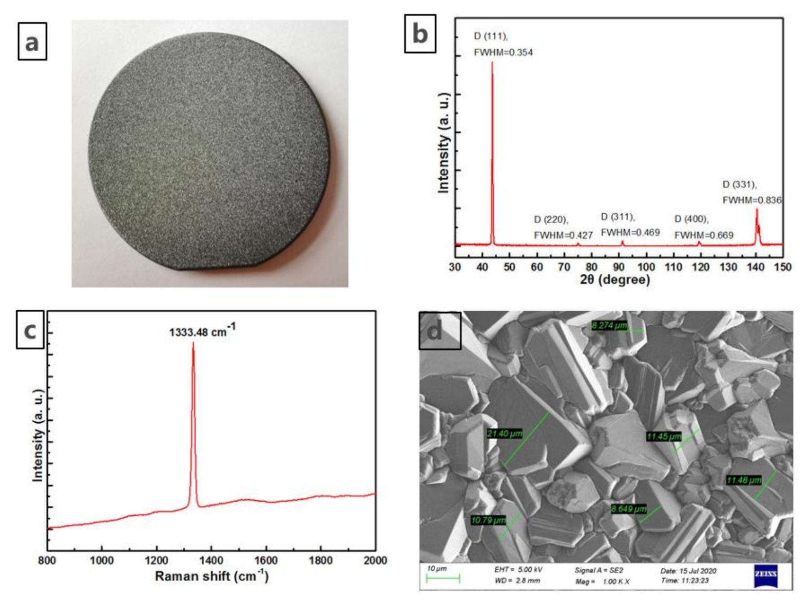
To evaluate the morphology and crystallinity of the diamond films grown by MPACVD, X-ray diffraction (XRD), Raman spectroscopy, and scanning electron microscopy (SEM) techniques have been employed. Figure 1a shows a photograph of a 2-inch 350 µm-thick diamond film obtained on a Si substrate. Figure 1b shows the XRD spectrum of the sample. The XRD patterns clearly shows the polycrystalline diamond phase by showing (111), (220), (311), (400) and (311) reflection peaks with the most intense peak at a (111) orientation. Figure 1c shows the Raman spectrum of the diamond films grown by MPACVD. From the figure, we confirm that there is single sharp and intense diamond peak at 1333.48 cm−1 without non-diamond contribution. Figure 1d shows the surface morphology of the diamond film sample measure by scanning electron microscopy (SEM).
2.1. Grinding
To reduce surface roughness of diamond film, a grinding method can be used by adding titanium to the vitrified bond wheel. By using the grinding wheel, the surface roughness of CVD diamond film can be dramatically reduced [19].
Here, as the first step, 2-inch diamond samples grown on Si by MPACVD were ground against an iron plate using diamond slurry to prepare flat diamond faces. The grinding of diamond was conducted on a rotating plate. The rotating plate is made of iron with a diameter of ~300 mm. The sample was attached to the sample holder, which was placed on the iron plate and rotated during grinding. The grinding pressure was applied to the sample by adding a suitable weight. To obtain a smooth diamond surface via grinding, it is critical to prepare an ideal flat iron plate and determine the optimal process parameters.
In this work, the grinding of diamond samples was performed under the following conditions. A pressure of 6200 Pa was applied to the samples with a constant distribution of the water-based diamond slurry containing diamond particles, sizes ranging from 10 μm to 40 μm (here called W10 toW40), and a grinding wheel rotation speed of 40 rpm. The grinding time was around 12 h and the removed thickness is 80 μm. After grinding, the sample was sequentially cleaned with acetone and alcohol in an ultrasonic bath.
To study the effect of diamond slurry size for the grinding process, we employed various combinations of diamond abrasives with different particle sizes for achieving the smooth surface. We employed 7 combinations, the particle sizes are 10, 20 and 40 μm, and change the sequence of usage W40, W40 to W20, W10, W20, W40 to W10, W20 to W10, and W40 to W20 to W10 to verify is most effective sequence and combination of diamond abrasives in reducing the roughness of the CVD diamonds surface.
2.2. Reactive Ion Etching-Inductively Coupled Plasma (RIE-ICP)
ICP is an effective technology to smooth the diamond surface with high throughput owing to its high plasma density. The total pressure, RF power, and gas composition, significantly influence the final roughness of diamond films [20]. The improved roughness of the etched diamond surface has been observed with an increase in the O2/CF4 ratio [21].
In our process, the ICP treatment was performed between the grinding and mechanical polishing processes as a transitional process to make the grinding surface flatter. Here, we employed the SF6- and O2-based two-step etching process to achieve a smooth diamond surface.
Here, we have examined the post-grinding surface treatment process by employing two types of plasma gases. In the SF6-based approach, the pressure, time and ICP power were kept at constant values, i.e., 1.34 Pa, 10 min, 500 W, respectively. The total gas flow was kept constant at 30 sccm. In the O2-based approach, we start with 2.5 min O2 followed by 0.5 min O2/CF4 plasma, the first step was carried out using 50 sccmO2 gas and fixed ICP power at 800 W while the pressure was 2 Pa. In order to improve the etching rate in O2 plasma etching, a second gas, CF4, is introduced to the process. The second step was performed using 40 sccm O2 and 10 sccm CF4 at 1.6 Pa, the ICP power was change to 200 W. Process parameters for both recipes are summarized in Table 1.
2.3. Mechanical Polishing
After the ICP process, mechanical polishing on a rotating resin-bonded diamond wheel was carried out to create an extremely smooth surface for the sample, which obtained a lower roughness in the ICP process.
We used a resin-bonded wheel charged with diamond abrasive grains. The experimental setup comprises a rotating table, pressure blocks, a sample holder, a cooling system, and a conditioner. Before the process, the wheel was conditioned to ensure a maximum contact area with the diamond. The polishing wheel was placed on the rotating table, which was kept at 1200 rpm rotating during polishing. To maintain a stable contact state between the diamond sample and polishing plate, the sample was fixed to a sample holder. The holder rotates and swings during the polishing process, at a pressure of 7400 Pa, using pressure blocks. The rotation speed, swing speed, and swing distance of the sample holder are 120 rpm, 40 rpm, 6 cm, respectively. The flow rate of the cooling water was kept at 10 mL/min, and we should ensure that the water did not fall on the polishing wheel. The polishing temperature influences the rate. Higher temperatures provide faster polishing; therefore, we kept the temperature at 50 °C. In the polishing process, the removed thickness is 15 μm.
3. Results and Discussion
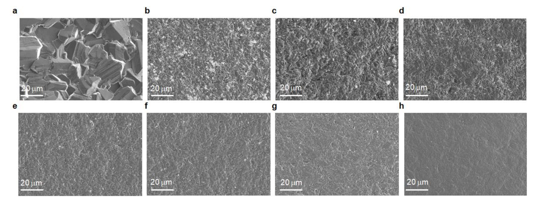
Figure 2a shows the SEM image (×1000) of an as-grown diamond surface. Figure 2b–h show the SEM image (×1000) of the grinded diamond film using various combinations of diamond abrasives. A number of large pits can be observed in Figure 2b,c, and it can be confirmed that the pollutant particles have embedded into the structures of the surface after the grinding process. However, the number of pits per unit area is visibly reduced with the decrease in Ra values during grinding. There are planes in the Figure 2d, although they are unevenly distributed. The grain boundary can be seen in Figure 2e–g. In Figure 2h, the planes are connected together, and the boundary of the grain becomes not very obvious. The micro-grains were flattened evenly in all planes and directions after the grinding process. With the change of diamond abrasive particles, the diamond surface becomes flatter.
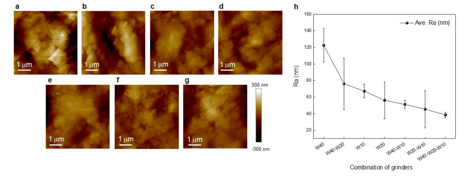
To further study the surface morphology of diamond film, contact mode atomic force microscopy (AFM) was employed after the grinding process. Figure 3a–g shows the AFM surface topography of the diamonds, these images show the same trend as Figure 2. From the scale bar, there are obvious protrusions and depressions on the surface at the beginning, the particle volume is also very large, and the roughness value begins to decrease with the change of diamond abrasive, gradually decreasing from 137 nm, 112 nm, 61.4 nm, 58 nm, 51.9 nm, 46.8 nm, to 39 nm, respectively, while Figure 3h shows the average roughness over the 25 μm2 of each ground diamond surface.
By using the combination of abrasives, we were able to confirm that the grinding process significantly enabled us to significantly reduce the surface roughness of polycrystalline diamond. Figure 3h shows the average surface roughness data against the abrasive diameter used for grinding. When the grinding particle size was employed in sequence from W40 to W20 to W10, the smoothest surface was achieved with a surface roughness of 32 nm. The same grit size of the diamond abrasives allows us to obtain the same grade surface roughness. In order to further enhance the surface quality, beyond a roughness of 30 nm, further polishing is necessary.
Therefore, 2 samples (sample a and sample b), after grinding by W40 to W20 to W10, with the better surface quality, were prepared for a further etching process.
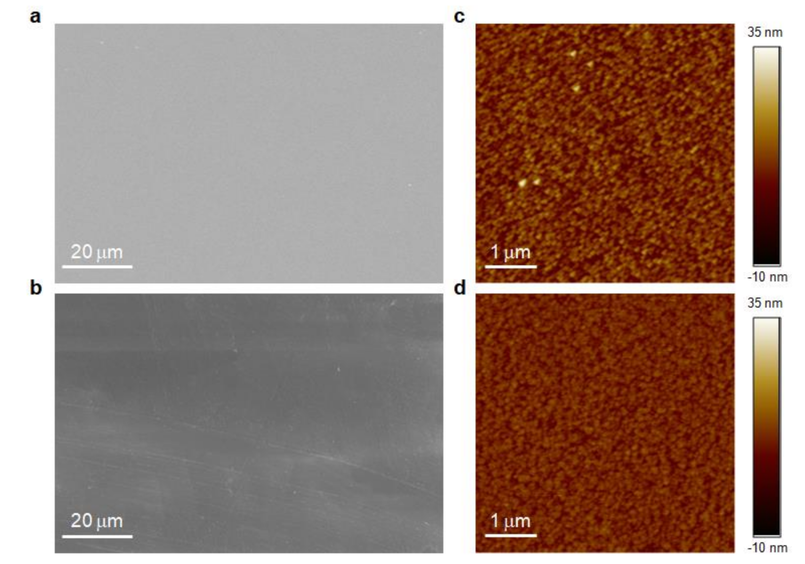
Figure 4a shows the SEM image of the CVD diamond surface after SF6 ICP etching (sample a). Sample a was evident from the SEM images without pits and grain boundaries. Figure 4b shows the SEM image of the CVD diamond after O2-O2/CF4 ICP (sample b). We were able to confirm that SF6 and O2-O2/CF4-based plasma etching further improves the smoothness of the diamond surface after grinding, and the roughness is reduced from 30 nm to less than 3 nm.
There was no obvious etch pits and defects observed across the surface. This indicates that there was no severe damage to the CVD diamond surface caused by the grinding process. Moreover, the variations in the material removal rates with different gases at a given etching time were calculated and summarized in Table 2. We chose commonly used diamond etching gases, chlorine-based gases and fluorine-based gases to obtain the etching rates. The ICP power was fixed at 400 W, several groups of different etching conditions were selected for the experiment, and the depth of the etched part was measured by a step meter, then the etching rate was calculated.
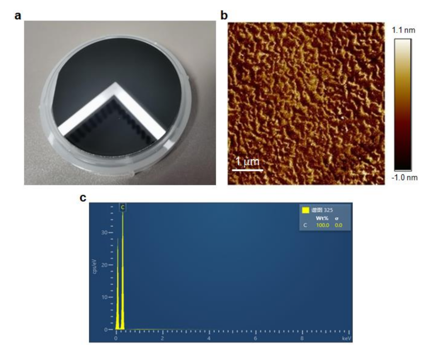
Figure 5a shows the photograph image of sample a after completing mechanical polishing process. Figure 5b shows the AFM surface topography of this CVD diamond sample after mechanical polishing. The roughness was evaluated over an area of 5 μm × 5 μm. The value of the surface roughness of the polished surface was 0.278 nm. It is clear that the diamond surface is not compact, resulting from ICP, was improved by mechanical polishing. The resultant surface integrity was high and the regularities on the surface was clear. Furthermore, the energy-dispersive spectroscope (EDS) signal confirms that there is no elemental contamination of a diamond sample surface from the polishing plate, as shown in Figure 5c.
There are the same mechanisms for the surface modification of the diamond film in the mechanical process and the CMP process, which is abrasion. In our work, the SEM and AFM images of Figure 2 and Figure 3 show a grinding action with different combinations of abrasive particles. The grinding begins with the removal of crystal peaks due to the contact with iron plate and diamond slurry, Thomas [22] proposed a chemical and mechanical removal mechanism in the reactions between the thin diamond film, polishing pad and silica abrasives, and show a steady polishing action with time. We did not add chemicals, so there is no oxidation mechanism in the grinding. Plasma etching [15] is based on the principle of sputtering and chemical reaction, and we similarly have high material removal rate as several microns per hour in whole process. Ultrasonic machining [16] in a slurry with diamond particles is based on the micro-chipping and form defects in a 3–6 μm thick sub-surface layer. Electrical discharge [17] with the removal mechanism of rapid evaporation, laser polishing of polycrystalline diamond coatings by transient thermal oxidation and/or evaporative ablation always have a micron-level roughness [18]. In our work, a combination of a three stage polishing process, grinding, ICP etching and mechanical polishing improve the surface smoothness to the nanometer scale compared to the conventional technology.
4. Conclusions
Although diamond thermal spreaders of a small size have been effectively demonstrated, there are still several technological issues to be solved. Diamond is the hardest known material, with a superior chemical and thermal stability; therefore, there are various technical challenges such as a low material removal rate, film delamination, fragmentation, micro scratches, and contamination. To alleviate these issues, we have demonstrated the procedure to grow and polish thermally grade polycrystalline diamond using MPACVD and the compound approach of grinding, ICP, and mechanical polishing, atomically smooth surfaces without the formation of sub-surface damage, and etch pits were obtained, respectively.
In this study, we investigated the effects of the processing method on a diamond with a size of 2-inch. The processing method consisting of (1) grinding using diamond slurry size of different combinations, the surface roughness is reduced from 900 nm to 32 nm when the grinding particle size was employed sequence from 40 µm to 20 µm to 10 µm. (2) ICP etching using different gas, the surface roughness is reduced from 32 nm to 1.79 nm when the SF6 gas was employed, and (3) final mechanical polishing using a resin-bonded diamond wheel, the surface roughness is reduced from 1.79 nm to 0.315 nm.
According to the experimental observations, we conclude that for final surface roughness, sequential process of grinding, ICP etching, and finally mechanical polishing provided the most smooth surface of polycrystalline diamond. The proposed method of super-finishing diamond surface provides a surface roughness of 0.3–0.5 nm. We believe that the atomically smooth diamond surface enabled by our process has potential to be employed in widespread applications as a thermal spreader for efficiency heat dissipation.
Author Contributions
Data curation, B.W.; Funding acquisition, C.Z.; Investigation, Z.G.; Project administration, X.Z.; Writing—original draft, X.H. All authors have read and agreed to the published version of the manuscript.
Funding
This research was funded by the foundation from Department of Science and Technology of Fujian Province (China, Grant Nos. 2020J01704, 2019L3008), the Scientific Research Foundation from Jimei University (China, Grant Nos. ZP2020066, ZP2020065).
Institutional Review Board Statement
Not applicable.
Informed Consent Statement
Not applicable.
Data Availability Statement
The data presented in this study are available on request from the corresponding author.
Acknowledgments
We acknowledge the foundation from Department of Science and Technology of Fujian Province (China, Grant Nos. 2020J01704, 2019L3008), the Scientific Research Foundation from Jimei University (China, Grant Nos. ZP2020066, ZP2020065).
Conflicts of Interest
The authors declare no conflict of interest.
References
- Malshe, A.P.; Park, B.S.; Brown, W.D.; Naseem, H.A. A review of techniques for polishing and planarizing chemically vapor-deposited (CVD) diamond films and substrates. Diam. Relat. Mater. 1999, 8, 1198–1213. [Google Scholar] [CrossRef]
- Seelmann-Eggebert, M.; Meisen, P.; Schaudel, F.; Koidl, P.; Vescan, A.; Leier, H. Heat-spreading diamond films for GaN-based high-power transistor devices. Diam. Relat. Mater. 2001, 10, 744–749. [Google Scholar] [CrossRef]
- Zhang, Z.; Schneider, H.; Tounsi, P. A promising solution using CVD diamond for efficient cooling of power devices. Mater. Sci. Eng. B 2012, 177, 1358–1361. [Google Scholar] [CrossRef]
- Lions, M.; Saada, S.; Bazin, B.; Pinault, M.-A.; Jomard, F.; Andrieu, F.; Faynot, O.; Bergonzo, P. Extreme insulating ultrathin diamond films for SOD applications: From coalescence modelling to synthesis. Diam. Relat. Mater. 2010, 19, 413–417. [Google Scholar] [CrossRef]
- Liang, J.; Nakamura, Y.; Ohno, Y.; Shimizu, Y.; Nagai, Y.; Wang, H.; Shigekawa, N. Room temperature direct bonding of diamond and InGaP in atmospheric air. Funct. Diam. 2021, 1, 110–116. [Google Scholar] [CrossRef]
- Wang, K.; Ruan, K.; Hu, W.; Wu, S.; Wang, H. Room temperature bonding of GaN on diamond wafers by using Mo/Au nano-layer for high-power semiconductor devices. Scr. Mater. 2020, 174, 87–90. [Google Scholar] [CrossRef]
- Gerrer, T.; Cimalla, V.; Waltereit, P.; Müller, S.; Benkhelifa, F.; Maier, T.; Czap, H.; Ambacher, O.; Quay, R. Transfer of AlGaN/GaN RF-devices onto diamond substrates via van der Waals bonding. Int. J. Microw. Wirel. Technol. 2018, 10, 666–673. [Google Scholar] [CrossRef] [Green Version]
- Hicks, M.-L.; Pakpour-Tabrizi, A.C.; Jackman, R.B. Polishing, preparation and patterning of diamond for device applications. Diam. Relat. Mater. 2019, 97, 107424. [Google Scholar] [CrossRef]
- Yamamura, K.; Emori, K.; Sun, R.; Ohkubo, Y.; Endo, K.; Yamada, H.; Chayahara, A.; Mokuno, Y. Damage-free highly efficient polishing of single-crystal diamond wafer by plasma-assisted polishing. CIRP Ann. 2018, 67, 353–356. [Google Scholar] [CrossRef]
- Watanabe, J.; Touge, M.; Sakamoto, T. Ultraviolet-irradiated precision polishing of diamond and its related materials. Diam. Relat. Mater. 2013, 39, 14–19. [Google Scholar] [CrossRef]
- Kubota, A.; Takita, T. Novel planarization method of single-crystal diamond using 172 nm vacuum-ultraviolet light. Precis. Eng. 2018, 54, 269–275. [Google Scholar] [CrossRef]
- Friel, I.; Clewes, S.L.; Dhillon, H.K.; Perkins, N.; Twitchen, D.J.; Scarsbrook, G.A. Control of surface and bulk crystalline quality in single crystal diamond grown by chemical vapour deposition. Diam. Relat. Mater. 2009, 18, 808–815. [Google Scholar] [CrossRef] [Green Version]
- Lee, C.L.; Gu, E.; Dawson, M.D.; Friel, I.; Scarsbrook, G.A. Etching and micro-optics fabrication in diamond using chlorine-based inductively coupled plasma. Diam. Relat. Mater. 2008, 17, 1292–1296. [Google Scholar] [CrossRef]
- Mi, S.; Toros, A.; Graziosi, T.; Quack, N. Non-contact polishing of single crystal diamond by ion beam etching. Diam. Relat. Mater. 2019, 92, 248–252. [Google Scholar] [CrossRef]
- Man, W.D.; Wang, J.H.; Wang, C.X.; Wang, S.G.; Xiong, L.W. Planarizing CVD diamond films by using hydrogen plasma etching enhanced carbon diffusion process. Diam. Relat. Mater. 2007, 16, 1455–1458. [Google Scholar] [CrossRef]
- Ralchenko, V.G.; Ashkinazi, E.E.; Zavedeev, E.V.; Khomich, A.A.; Bolshakov, A.P.; Ryzhkov, S.G.; Sovyk, D.N.; Shershulin, V.A.; Yurov, V.Y.; Rudnev, V.V. High-rate ultrasonic polishing of polycrystalline diamond films. Diam. Relat. Mater. 2016, 66, 171–176. [Google Scholar] [CrossRef]
- Zhang, F.L.; Wang, C.Y.; Guo, Z.N.; Chen, J. Effect of Electrical Spark Discharging Parameters on the Etching of Chemical Vapor Deposition (CVD) Diamond Film. Mater. Manuf. Processes 2007, 22, 859–864. [Google Scholar] [CrossRef]
- Prieske, M.; Vollertsen, F. Picosecond-laser polishing of CVD-diamond coatings without graphite formation. Mater. Today Proc. 2020, 40, 1–4. [Google Scholar] [CrossRef]
- Xu, H.; Zang, J.; Tian, P.; Yuan, Y.; Wang, Y.; Yu, Y.; Lu, J.; Xu, X.; Zhang, P. Surface conversion reaction and high efficient grinding of CVD diamond films by chemically mechanical polishing. Ceram. Int. 2018, 44, 21641–21647. [Google Scholar] [CrossRef]
- Izak, T.; Kromka, A.; Babchenko, O.; Ledinsky, M.; Hruska, K.; Verveniotis, E. Comparative study on dry etching of polycrystalline diamond thin films. Vacuum 2012, 86, 799–802. [Google Scholar] [CrossRef]
- Ando, Y.; Nishibayashi, Y.; Kobashi, K.; Hirao, T.; Oura, K. Smooth and high-rate reactive ion etching of diamond. Diam. Relat. Mater. 2002, 11, 824–827. [Google Scholar] [CrossRef]
- Thomas, E.L.H.; Nelson, G.W.; Mandal, S.; Foord, J.S.; Williams, O.A. Chemical mechanical polishing of thin film diamond. Carbon 2014, 68, 473–479. [Google Scholar] [CrossRef] [Green Version]
Figure 1.
(a) Photo of as-grown diamond surface; (b) XRD spectra taken on as-grown surface; (c) Raman spectra taken on as-grown surface; (d) SEM micrographs of as-grown film.
Figure 1.
(a) Photo of as-grown diamond surface; (b) XRD spectra taken on as-grown surface; (c) Raman spectra taken on as-grown surface; (d) SEM micrographs of as-grown film.

Figure 2.
SEM micrographs of as grown and ground diamond films, the films ground by different combinations of abrasive particles. (a)As-grown; (b) W40; (c) W40 to W20; (d) W10; (e) W20; (f) W40 to W10; (g) W20 to W10; (h) W40 to W20 to W10. W is the diameter of abrasive particles, W40, W20, W10 represent the diameter of diamond abrasive in grinding is 40 μm, 20 μm, 10 μm, respectively. The (b,d,e) mean that only one grain size abrasive is used; (c,f,g) mean that two kinds of abrasives have been used successively; (h) means that abrasives with three particle sizes are used in sequence.

Figure 3.
Corresponding AFM surface topography of diamond films ground by different combinations of abrasive particles (5 × 5 μm2). (a) W40; (b) W40 to W20; (c) W10; (d) W20; (e) W40 to W10; (f) W20 to W10; (g) W40 to W20 to W10. The value of (a–g) is 137, 112, 61.4, 58, 51.9, 46.8, 39 nm, respectively. (h) The evolution of the roughness gives a linear decrease with diameter of diamond particles in the slurry.

Figure 4.
(a) SEM micrographs for diamond surface after etching in SF6 (30 sccm, 10 min, ICP power = 500 W); (b) SEM micrographs for diamond surface after etching in O2 (50 sccm, 2.5 min, ICP power = 800 W)—O2/CF4 (40/10 sccm, 0.5 min, ICP power = 200 W); (c) AFM surface topography for the uniform and loose surface formed at (a) conditions, Ra = 1.79 nm, and (d) AFM surface topography for the scattered surface formed at (b) conditions, Ra = 2.82 nm. The loose surface formed during etching is beneficial for material removal in mechanical polishing.

Figure 5.
(a) 2-in polished diamond wafer (sample a); (b) typical AFM micrographs of film after polishing, Ra = 0.278 nm. 2-inch diamond wafer fabricated using mechanical polishing, exhibiting an ultra-smooth surface of average Ra = 0.315 nm (over the 10 scans); (c) EDS spectrum of the polished diamond wafer.


Table 1.
Diamond etching process parameters.
| No. | Gas | Flow Rate | ICP Power | Platen Power | Pressure | Duration |
|---|---|---|---|---|---|---|
| a | SF6 | 30 sccm | 500 W | 50 W | 1.34 Pa | 10 min |
| b-1st | O2 | 50 sccm | 800 W | 100 W | 2 Pa | 2.5 min |
| b-2nd | O2/CF4 | 40/10 sccm | 200 W | 0 W | 1.6 Pa | 0.5 min |
Table 2.
Diamond etching removal rates.
| Gas | Flow Rate | ICP Power | Platen Power | Pressure | Rate |
|---|---|---|---|---|---|
| SF6 | 80 sccm | 400 W | 100 W | 1 Pa | 0.39 μm/h |
| O2/CF4 | 80/25 sccm | 400 W | 100 W | 1 Pa | 1.02 μm/h |
| Ar/Cl2 | 25/80 sccm | 400 W | 300 W | 0.8 Pa | 2.34 μm/h |
Publisher’s Note: MDPI stays neutral with regard to jurisdictional claims in published maps and institutional affiliations. |
© 2022 by the authors. Licensee MDPI, Basel, Switzerland. This article is an open access article distributed under the terms and conditions of the Creative Commons Attribution (CC BY) license (https://creativecommons.org/licenses/by/4.0/).
Share and Cite
MDPI and ACS Style
Huang, X.; Zhou, C.; Wu, B.; Geng, Z.; Zhang, X. Wafer-Scale Polishing of Polycrystalline MPACVD-Diamond. Surfaces 2022, 5, 155-164. https://0-doi-org.brum.beds.ac.uk/10.3390/surfaces5010008
AMA Style
Huang X, Zhou C, Wu B, Geng Z, Zhang X. Wafer-Scale Polishing of Polycrystalline MPACVD-Diamond. Surfaces. 2022; 5(1):155-164. https://0-doi-org.brum.beds.ac.uk/10.3390/surfaces5010008
Chicago/Turabian StyleHuang, Xuerun, Changjie Zhou, Bo Wu, Zhiming Geng, and Xing Zhang. 2022. "Wafer-Scale Polishing of Polycrystalline MPACVD-Diamond" Surfaces 5, no. 1: 155-164. https://0-doi-org.brum.beds.ac.uk/10.3390/surfaces5010008