Light-Induced Effects in Amorphous Chalcogenide Glasses: Femtoseconds to Seconds


1
Department of Physics and Bernal Institute, University of Limerick, V94T9PX Limerick, Ireland
2
Department of Physics, Indian Institute of Science Education and Research, Bhopal 462066, India
*
Author to whom correspondence should be addressed.
Physics 2021, 3(2), 255-274; https://0-doi-org.brum.beds.ac.uk/10.3390/physics3020019
Submission received: 27 February 2021
/
Revised: 26 March 2021
/
Accepted: 10 April 2021
/
Published: 26 April 2021
(This article belongs to the Section Applied Physics)
Abstract
:Amorphous chalcogenide glasses are intrinsically metastable, highly photosensitive, and therefore exhibit numerous light-induced effects upon bandgap and sub-bandgap illumination. Depending on the pulse duration of the excitation laser, ChGs exhibit a series of light-induced effects spanning over femtosecond to seconds time domain. For continuous wave (CW) illumination, the effects are dominantly metastable in terms of photodarkening (PD) and photobleaching (PB) that take place via homopolar to heteropolar bond conversion. On the other hand, under nanosecond and ultrafast pulsed illumination, ChGs exhibit transient absorption (TA) that is instigated from the transient bonding rearrangements through self-trapped exciton recombination. In the first part of the review, we pay special attention to continuous wave light-induced PD and PB, while in the second part we will focus on the TA and controlling such effects via internal and external parameters, e.g., chemical composition, temperature, sample history, etc.
1. Introduction
Amorphous chalcogenide glasses (a-ChGs) consist of covalently bonded chalcogen elements which belong to group 16 of the periodic table e.g., sulphur (S), selenium (Se), and tellurium (Te) and are formed in conjugation with the elements of group 15 (Sb, As) or group 14 (Ge, Si) [1]. The bandgap of the ChGs lies within the range of 1–3 eV [2]. ChGs possess a remarkable property of transparency in the wide infrared (IR) region which makes them a promising candidate for infrared cameras [3], planar waveguides for integrated optics [4], and infrared sensors [5]. Additionally, these glasses have high chemical resistance to extremely corrosive media, and they can tune their physical and chemical properties over a wide range by changing the composition [6,7]. Among the several families of ChGs, the most widely studied systems are the binary As-S (Se) and Ge-S (Se), the ternary Ge-As-S (Se), and Ge-Sb-Te (Se, S).
ChGs are distinguished from other materials by their unique photosensitivity to bandgap or sub-bandgap illumination, which is depicted by numerous photo-induced effects related to its structure and properties [1,8]. Photoinduced processes are typically linked with changes in optical parameters, mainly the bandgap energy and variation of the refractive index. Photoinduced changes in amorphous ChGs are associated with the generation of electron-hole (e-h) pairs [9,10]. The absorption of a photon may result in the forming, separating, or recombining of an electron-hole pair. The separation of the e-h pair leads to changes in the electrical response of the material, which may give rise to photoconductivity [11]. On the other hand, radiative e-h recombination leads to photoluminescence, whereas non-radiative recombination of the e-h pair results in photo structural and optical changes in the material [12].
Photoinduced effects in ChGs are generally classified in terms of reversibility/irreversibility. The reversibility is defined by its ability to recover to the initial state, i.e., before irradiation. Reversible effects are of two types: metastable and transient. Metastable effects can be recovered by heating the material near the glass transition temperature (g), whereas transient effects persist only during illumination [13]. In contrast, irreversible effects are mostly permanent changes that can only be reversed by heating it above g, even close to the melting point of the sample.
Metastable and transient photoinduced effects can also be distinguished by varying the pulse width of the excitation laser. Depending on the duration of the laser pulses, photoinduced effects vary significantly. It was shown by numerous previous studies that photodarkening (PD) and photobleaching (PB) are the two light-induced effects unique to ChGs when illuminated with continuous wave bandgap or sub-bandgap light [8,13,14]. On the other hand, for the nanosecond and ultrafast pulsed laser illumination, transient absorption (TA) is most commonly observed [15,16]. In this review, we will discuss the time evolution of photoinduced effects in ChGs in two parts. In the first part, we will discuss continuous wave (CW) laser-induced PD and PB that take place between seconds to hours, while in the second part we focus on TA and its evolution in the picosecond to microsecond time scale.
2. Continuous Wave (CW) Light-Induced Effects in ChGs
PD and PB are characterized by the light-induced shift in the absorption edge towards longer and shorter wavelengths. PD is defined by a reduction of optical bandgap, i.e., the absorption edge of the material redshifts to longer wavelengths or lower photon energies, and the material becomes darker with a decrease in transmission [13,14]. The phenomenon of PD was first reported by Berkes et al. [17] on a 1 μm film of As2Se3 that was exposed to focused microscope light. PD is mostly observed in the arsenic (As) based ChGs and is believed to originate from light-induced reduction of homopolar bonds to energetically favorable heteropolar bonds [18,19]:
Here “Ch” represents the chalcogen element and “” represents laser illumination. Importantly, PD consists of a transient and metastable part [14,18,20]. When illumination is switched off after the complete saturation of PD, there is an appreciable transient decay, but some switched bonds remain frozen in a metastable state that can only be reversed by annealing the sample near g [13].
In stark contrast to PD, PB is characterized by a blue shift (to shorter wavelength) of the optical absorption edge, i.e., the optical bandgap of the material increases, and by the fact that the sample becomes transparent, i.e., transmission increases [8,21]. Unlike PD, PB cannot be reversed by heat treatment. PB is most commonly observed in germanium (Ge) based ChGs, which can be understood in terms of two parallel mechanisms. The first mechanism is intrinsic structural changes described by the following equation [18,22]:
The second mechanism includes the photo-oxidation of Ge atoms by the creation of Ge-O bonds at the expense of Ge-Ge bonds that are broken by illumination [22,23,24]. PB is very sensitive to material composition and deposition techniques. Importantly, the refractive index of the material changes upon PD/PB, which might be useful for fabricating optical devices.
2.1. Photodarkening in As-Based ChGs
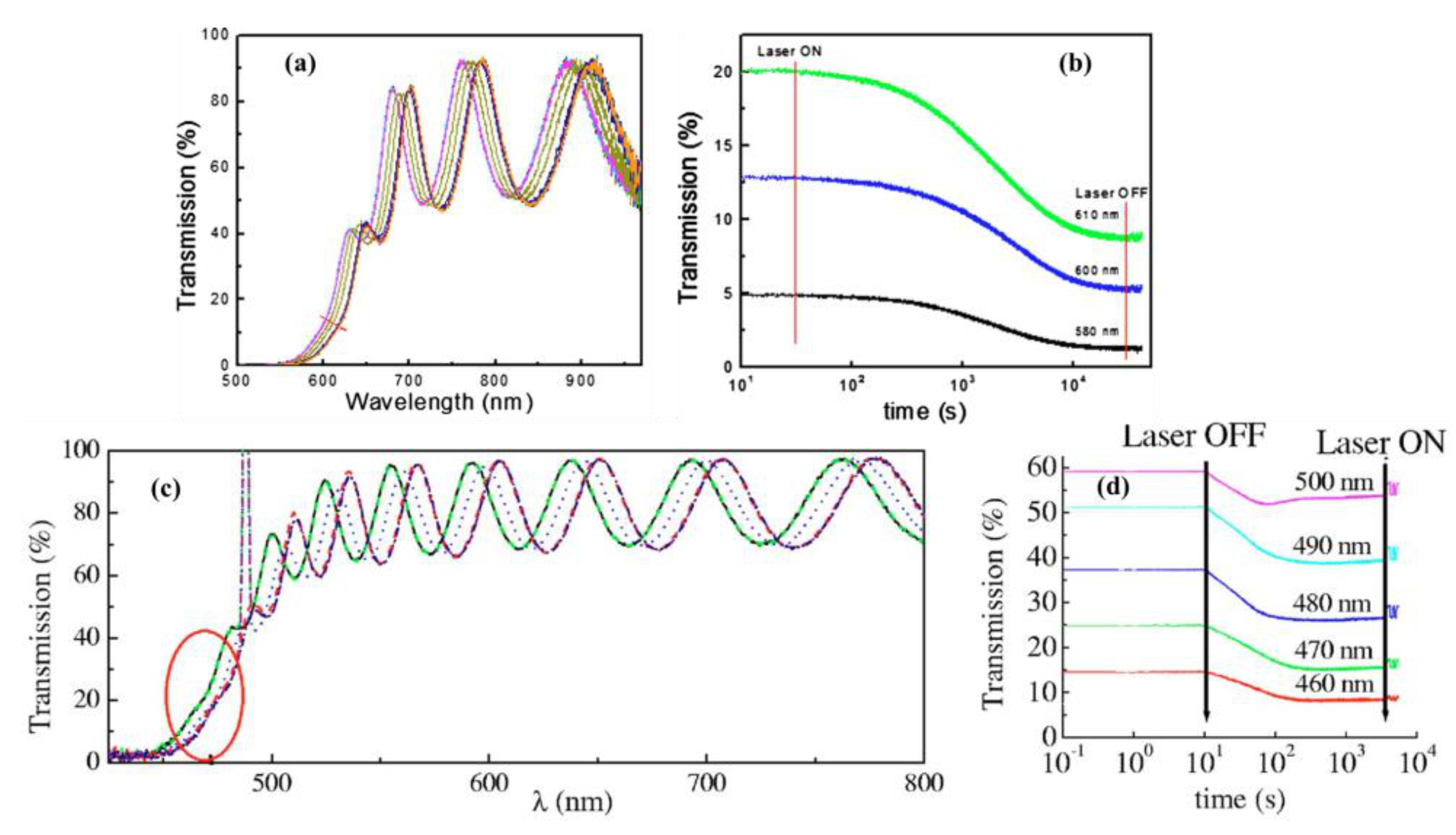
As2S3 and As2Se3 are most commonly known As-based ChGs, which are studied extensively for light-induced effects [13,25,26]. In-situ transmission measurements—in other words, CW pump-probe measurements—are often used to demonstrate the light-induced effects in ChGs. It can be seen from Figure 1a that transmission spectra of As2Se3 ChGs thin films (with thickness of 0.7–1 μm near the optical absorption edge) gradually redshifts upon 660 nm CW laser illumination to demonstrate PD [26]. This leads to an associated decrease in transmission, as shown in Figure 1b at three different fixed probe wavelengths. When the laser is switched on, for all the wavelengths, transmission decreases continuously before reaching a plateau. Similar PD is also observed in 1 μm thin As2S3 film, as demonstrated by the work of Ganjoo and Jain [13]. When illuminated with a 488 nm CW laser, optical transmission spectra of As2Se3 redshifts (Figure 1c), as is characteristic of PD. The zoomed region is focused on the optical absorption edge near the bandgap. Likewise, following laser illumination, transmission decreases at all probe wavelengths, as shown in Figure 1d. It is important to note that light-induced effect consists of two parts: transient and metastable. The transient component exists only during illumination, while the existing permanent change after illumination is referred as metastable. We will discuss both of these in the following section.
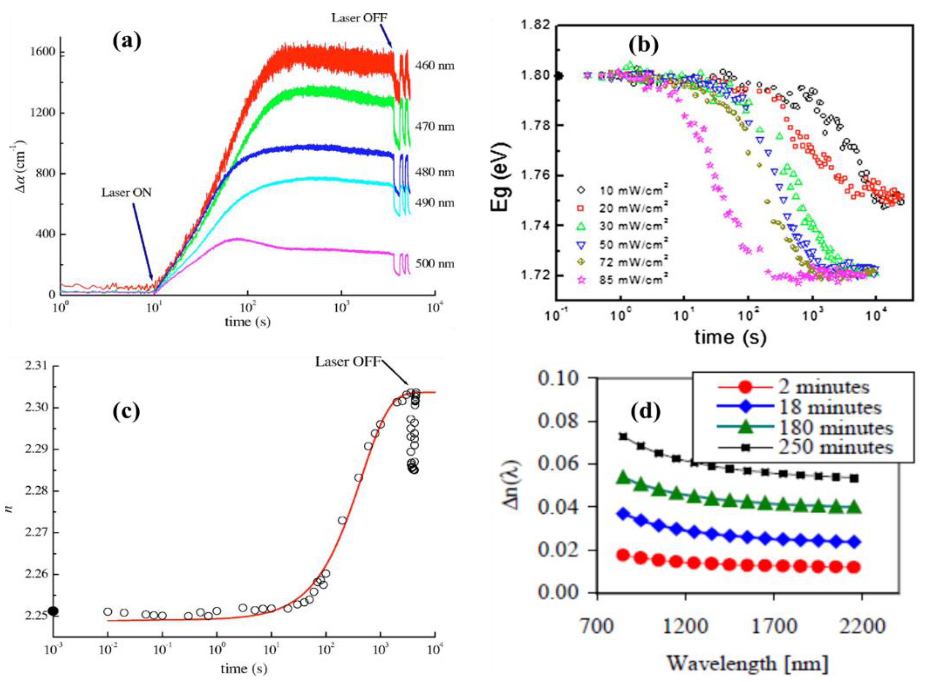
Similar to transmission, PD leads to a change in absorption coefficient Δα for all probe wavelengths. Since Δα = (−1/d)ln(/0), ( refers to the transmission at any time , 0 refers to the transmission at time = 0, d refers to the thickness of the film) decrease in the transmission is reflected by the increase in Δα upon PD, as shown in Figure 2a. The transient part of the changes is understood from the several on–off cycles of laser illumination which are further zoomed in the inset. When the laser is switched on, Δα increases monotonically and reaches a plateau. When the laser is switched off, Δα decreases and saturates quickly but never reaches the value before the illumination. This decreased part of Δα is termed as transient, while the saturated portion that remains after illumination is defined as metastable. When the laser is switched on subsequently, Δα increases again and the transient part reappears, reaching the same value as the saturated value in the first illumination. Noteworthy to mention, repeated on and off cycles only induced the transient part.
Since the absorption coefficient Δα changes significantly near the optical absorption edge, the bandgap of the material also changes following PD. Figure 2b shows the time evolution of the optical bandgap, g, in As2S3 [26]. g decreases slowly for the initial period, which is followed by steep decrease before reaching the plateau. The change in bandgap is higher as well as faster for higher laser intensity (pink curve) and less and slower for lower intensities. Quantitatively, Sati et al. [26] demonstrated that change in bandgap Δg is 0.05 eV at a laser intensity of 10 mW/cm2, whereas it increases to 0.08 eV when illuminated with an intensity of 85 mW/ cm2. Apart from that, the characteristic decay time of PD also changes dramatically, e.g., the kinetics of PD becomes faster from 3600 s to 50 s when the intensity increases from 10 to 85 W/ cm2.
Refractive index, n, is another important optical constant that changes significantly upon PD as shown in Figure 2c. For the practical application of ChGs in integrated optics, it is important to have a detailed understanding of the dynamic changes of n. Ganjoo and Jain [13] estimated the change in n from the fringes of the transmission spectra in Figure 1c by employing the Swanepoel method [28]. Following laser illumination, n initially increases slowly and then increases rapidly before reaching the plateau. Notably, n also comprises transient and metastable components like other optical parameters. Popta et al. [27] showed the wavelength dependence of the n in As2Se3 thin films by plotting it over a broad wavelength regime in near infrared (NIR), as shown in Figure 2d. The curve demonstrates the magnitude of the change in the real part of the refractive index at different exposure times, which is measured by subtracting it from the as-prepared value before laser illumination. Since the bandgap of As2Se3 is 1.76 eV (704 nm), the refractive index expected increases near the band edge toward 700 nm following the Kramers–Kronig relationship [29].
2.2. Photobleaching in Ge-Based ChGs
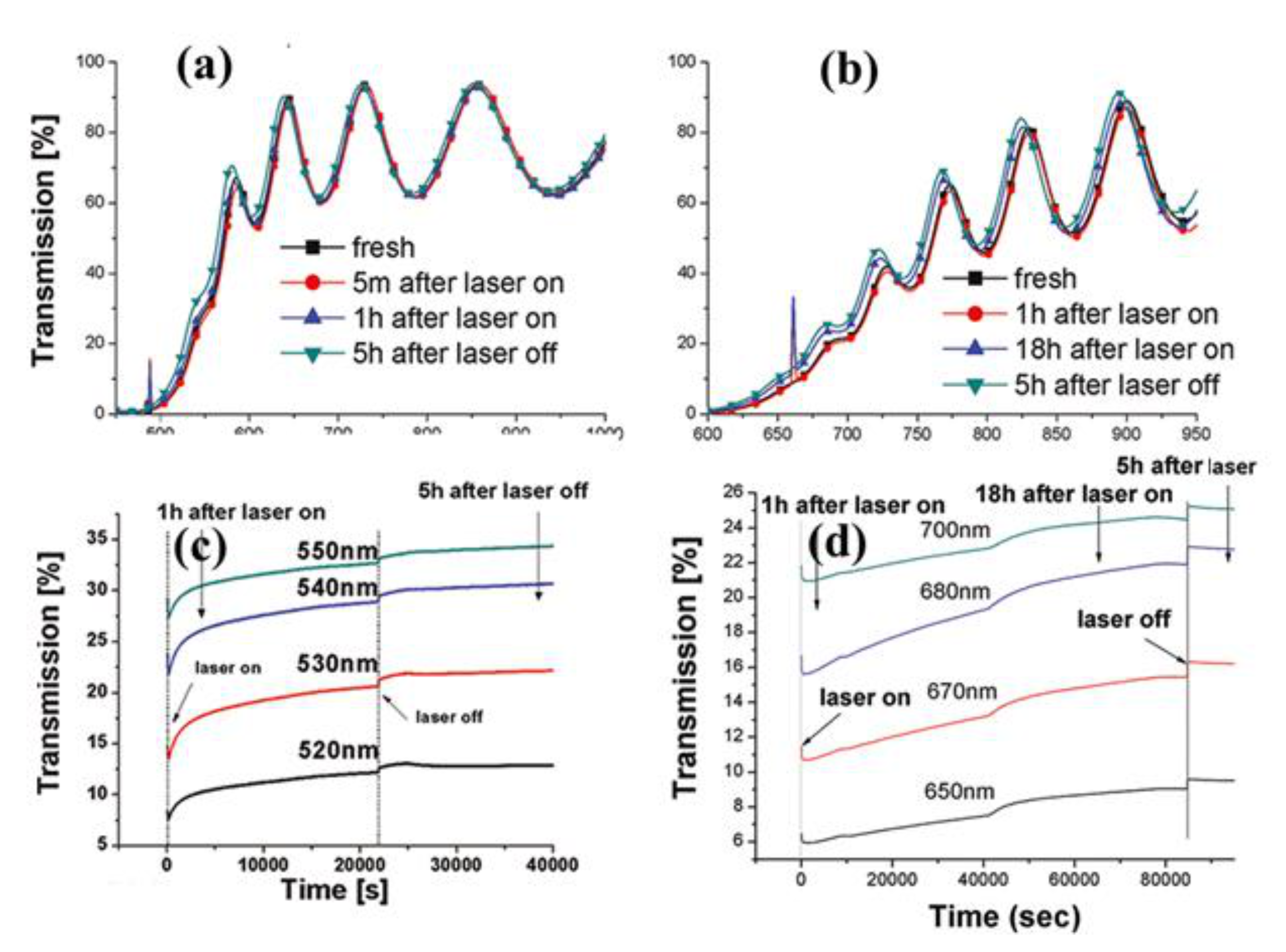
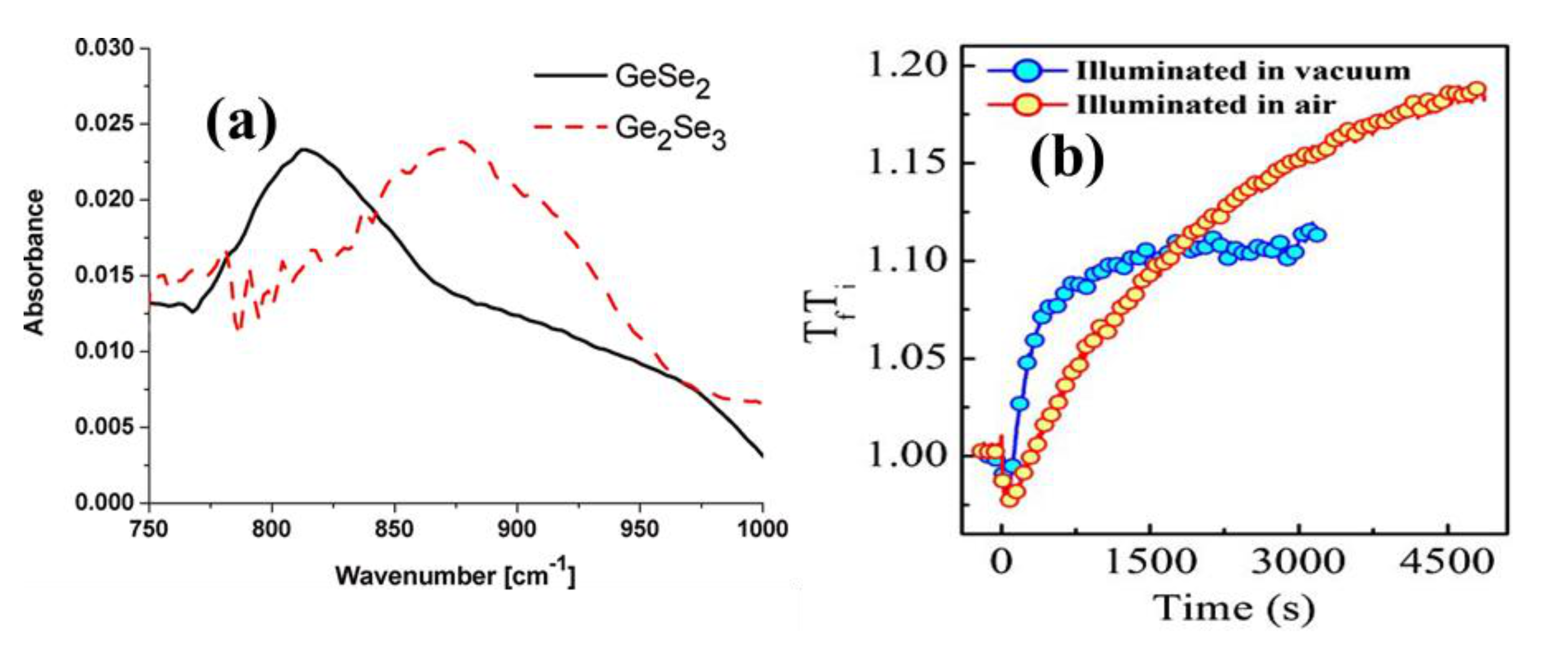
The PB in Ge-based ChGs was first observed by Lyubin in GeSe2 thin films (thickness 0.5 μm) with a 488 nm CW laser [21]. Similar PB was later observed in GeSe2 by Barik et al. using a 532 nm CW laser [30]. A more detailed study on PB was performed by Yan and co-workers in GeSe2 as well as in Ge-rich Ge2Se3 [22]. Figure 3a,b shows the optical transmission spectra of GeSe2 and Ge2Se3 thin films (thickness 1 μm) in as-prepared and when illuminated with 488 nm and 660 nm laser, respectively. Clearly, for the initial period of illumination, the spectra remain indistinguishable; however, with prolonged illumination, transmission spectra blueshift, a signature of PB. To get a detailed understanding of the kinetics of PB, the time evolution of the transmission at fixed probe wavelengths was recorded for both GeSe2 and Ge2Se3, as shown in Figure 3c and Figure 3d, respectively. Clearly, for both the samples, after an initial dip, transmission increases gradually, and final saturated transmission is much higher than initial transmission in line with PB. When the laser is turned off, transmission increases further, and the transient component saturates very quickly. Unlike PD, PB is believed to be originated not only from structural changes (Ge-Ge to Ge-Se) but also from the surface photooxidation of Ge atoms, i.e., formation of Ge-O bonds. In this regard, Figure 4a demonstrates the IR difference spectra before and after illumination for the samples. Since Ge2Se3 is rich in Ge-Ge bonds, photooxidation is predominant, as evinced by the strong GeO2 structural unit at 870 cm−1. On the other hand, in GeSe2, where the Ge content is less than Ge2Se3, oxidation takes place by forming chains of Se3-x-Ox-Ge-O-Ge-Ox-Se3-x clusters at 820 cm−1 [24,31]. Much later, we quantitatively demonstrated the relative contribution of structural changes and photooxidation to PB in Ge25As10Se65 thin films [32]. We recorded the in-situ transmission changes in air and in vacuum, where the oxygen concentration is negligible, and relative single wavelength transmission kinetics are shown in Figure 4b.
We found that the magnitude of PB in the air (ΔPBair = 0.21) is much larger compared to the magnitude of PB in the vacuum (ΔPBvac = 0.13), i.e., 62% of total changes in PB is associated with structural changes, while photooxidation plays a minor role in PB. Additionally, since photooxidation is a slower process, it makes the kinetics of PB in the air (τair = 1896 s) about ten times slower than in vacuum (τvac = 210 s).
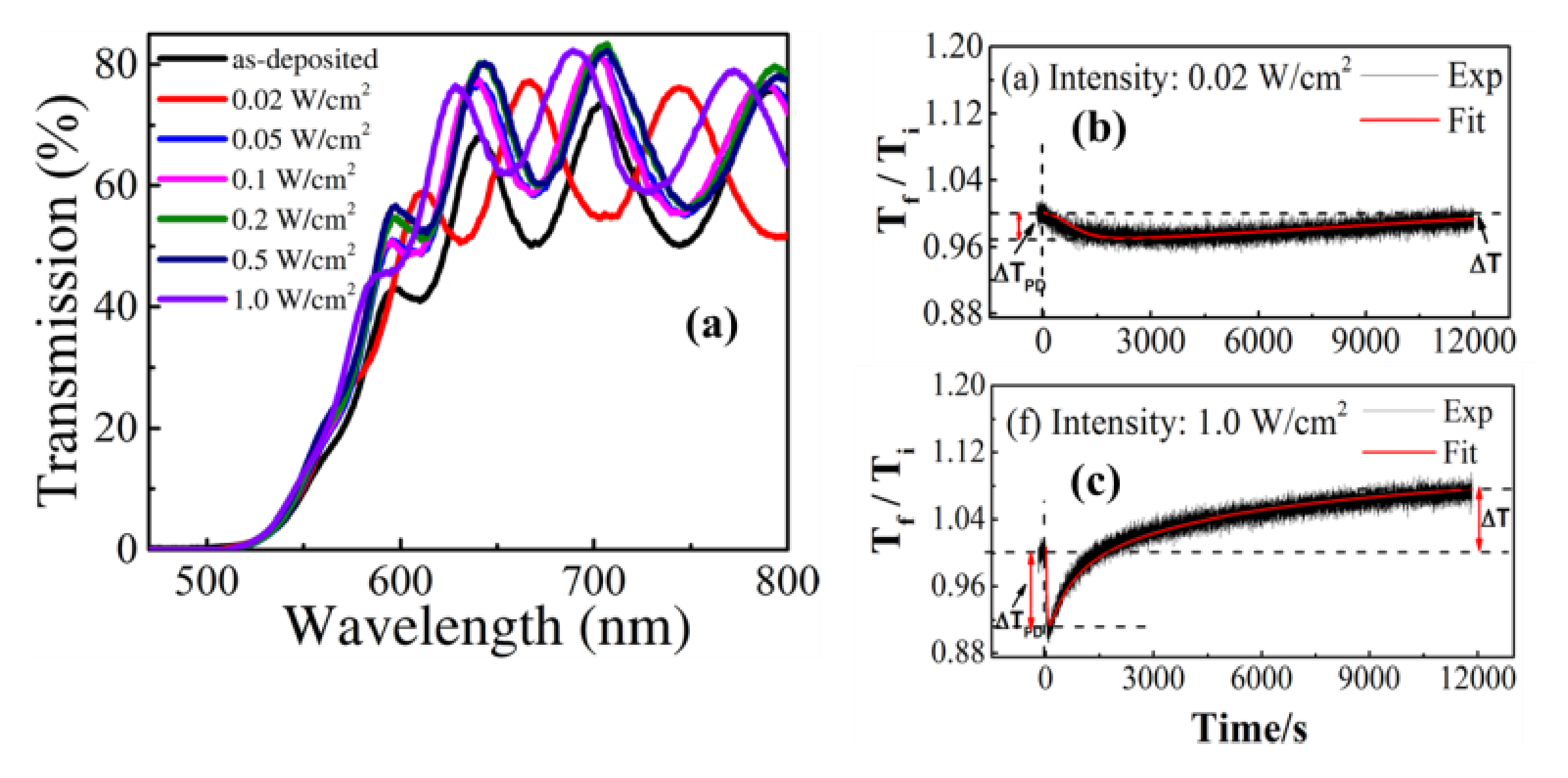
In another interesting work, Zhang et al. showed that prolonged illumination can lead to PB even in Ge-deficient Ge16.8Se83.2 thin films [33]. Figure 5a shows the transmission spectra of the sample when illuminated with a 655 nm CW laser for a period of 12,000 s at different intensities. Clearly, transmission spectra blueshifts to depict PB. To get more information, they investigated single wavelength kinetics at 560 nm at 0.02 and 1 W/cm2, as shown in Figure 3b,c. At 0.02 W/cm2, PD dominates with a very weak and slow PB, whereas the sample ends up in an overall PB state when illuminated with 1 W/cm2. Therefore, excitation intensity plays a critical role in determining the overall behavior of the sample. Apart from that, the kinetics of both PD and PB shows a strong dependence on laser power. For example, at 0.02 W/cm2, reaction time of PD (τPD = 1200 s) and (τPB = 11,000 s) is found to be two orders slower when compared to 1 W/ cm2, where τPD = 36 s and τPB = 280 s, respectively. In general, PD is instantaneous with laser illumination and always takes place faster than PB.
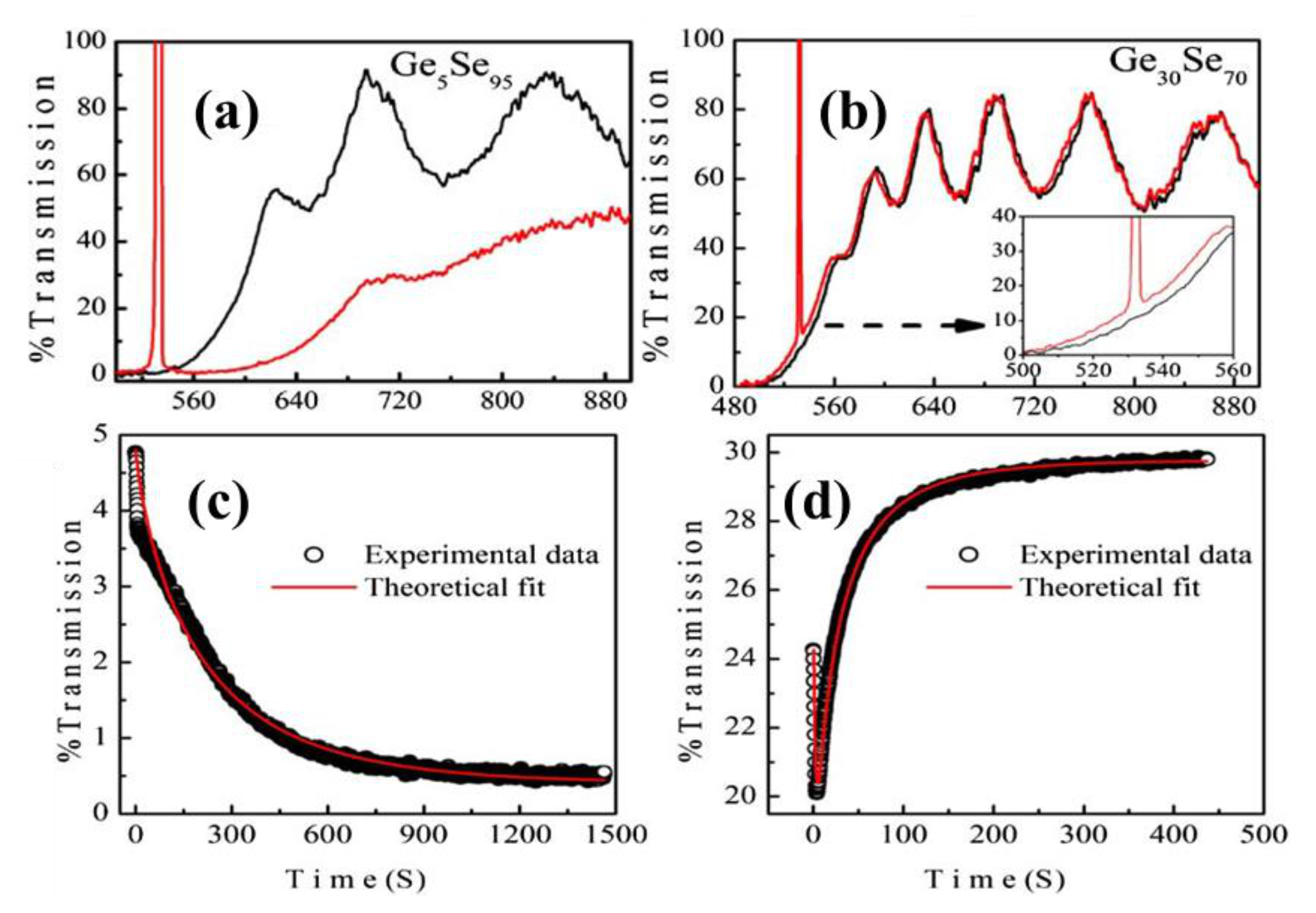
In line with more detailed work, Kumar et al. showed that by varying the relative composition of Ge and Se, they obtain a crossover from PD to PB in GexSe100-x thin films [34]. In this regard, Figure 6a,b shows the transmission spectra of Ge-deficient Ge5Se95 and Ge-rich Ge30Se70 thin films in as-prepared (black) and illuminated (red) states when illuminated with 532 nm CW laser. The strong, red-shifted absorption edge depicts PD in the former, while a weak blue shift in the latter demonstrates PB. Singe wavelength kinetics at 560 nm for Ge5Se95 and Ge30Se70 are shown in Figure 6c and Figure 6d, respectively. For Ge5Se95, the final transmission saturates much below the initial value in line with strong PD, whereas for Ge30Se70, the sample ends up in an overall PB state at the final stage of illumination.
2.3. Photodarkening and Photobleaching in Ternary Ge-As-Se
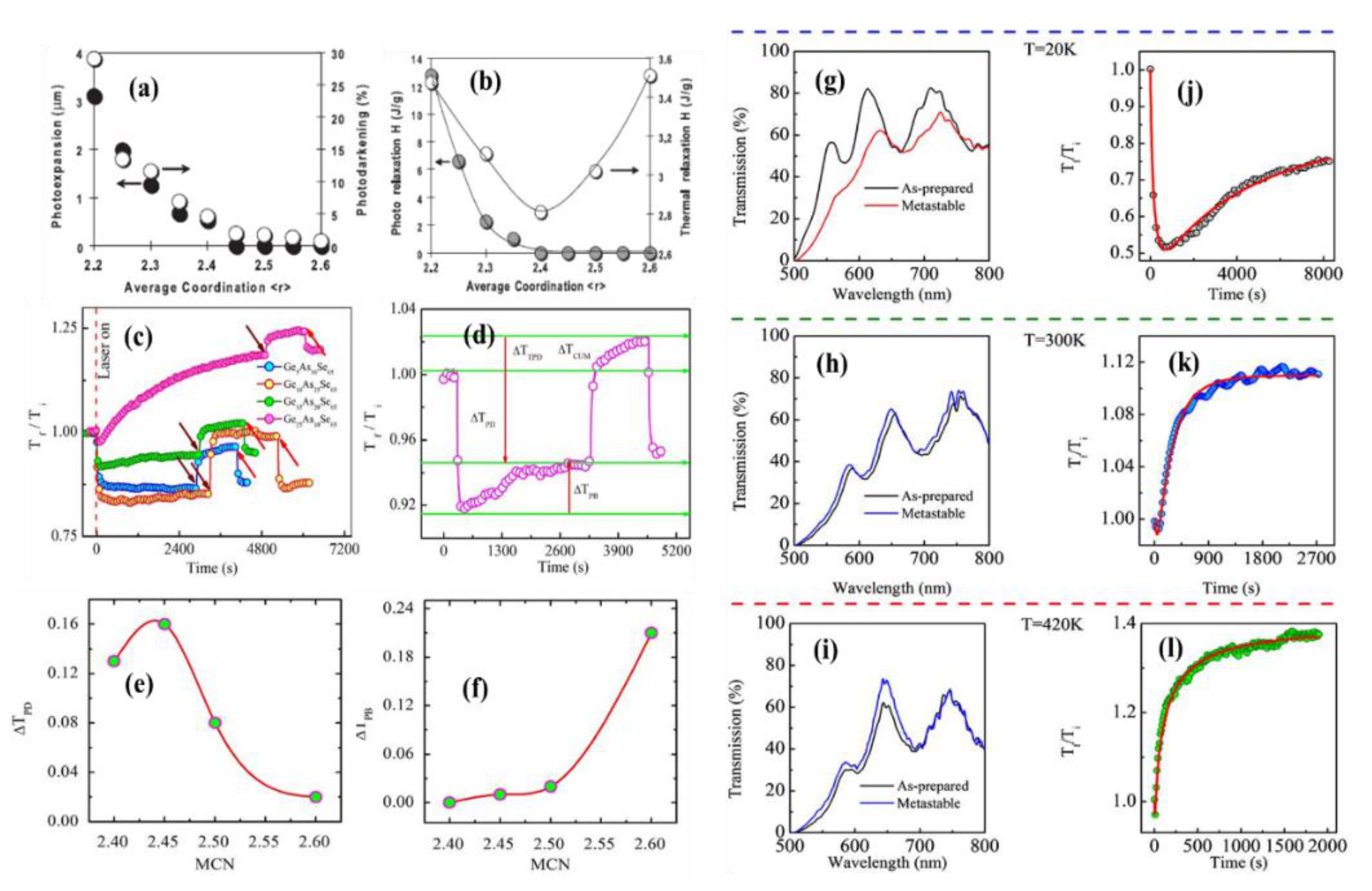
Ternary Ge-As-Se forms a special family of ChGs which shows the unusual coexistence of fast PD and slow PB under CW illumination [18]. Ge-As-Se is a prototype of ChGs and has advantages because of the similar size and electronegativity of the individual components that form a close-to-ideal network [35]. In ChGs, structural connectivity is usually quantified by the mean coordination number (MCN), which is denoted by ⟨⟩ and defined by the sum of the respective elemental concentrations times their covalent coordination number [36]. It was proposed by Phillips and Thorpe’s rigidity theory [37,38] that the physicochemical properties of ChGs depend strongly on the chemical composition [19,20] and likewise vary with ⟨⟩. From network rigidity theory, Philips [37] predicted that percolation transition at ⟨⟩ = 2.40 takes place from an under-constrained “floppy” network to an over-constrained “rigid” one. In particular, many previous studies by Lucas and Calvez with CW illumination have shown that properties like PD, photo relaxation, and photo expansion exhibit an extremum at ⟨⟩ = 2.4 with a monotonic decreasing trend, as shown in Figure 7a,b [6,35,39]. Notably, all samples for PD measurements were 1 mm thick polished discs. In stark contrast, our previous work established that chemical composition plays a major role and dominates over MCN in determining the light-induced effects [40]. In this regard, Figure 7c shows the single wavelength kinetics of a-GexAs35-xSe65 (x = 5, 10, 15 and 25) thin films of thickness 1 μm. Following the illumination with the pump beam, f/i (f and f represents final and initial transmission, respectively) decreases instantaneously for all samples to depict PD and eventually saturates within a few tens of seconds. After PD saturates completely, f/i gradually starts increasing in line with PB for all samples except x = 5. For the samples with x > 15, the final transmission saturates well above the as-prepared value whereas for the samples with x < 15, final transmission saturates below the initial transmission. After the transmission saturates to a PD/PB state, transient effect takes place after switching off the laser. To quantify the observed PD and PB, they are calculated the way as shown in Figure 7d. Figure 7e shows that unlike network rigidity theory, PD does not follow regular trend with MCN, i.e., disappears at MCN = 2.4, rather gradually decreases with increase in MCN. On the contrary, in Figure 7f we found that PB increases linearly with MCN till 2.5 with a sudden jump at 2.6. Such observations clearly indicate that PD and PB do not follow usual trend with MCN as predicted by network rigidity theory. In fact, chemical composition, i.e., Ge:As composition ratio plays the dominant role.
In this context, there are some other interesting works by Yang et al. [19], Zhang et al. [41], and Nemec et al. [42] who also demonstrated the CW laser illuminated light-induced effects in Ge-As-Se thin films.
So far, we have seen that chemical composition, prolonged illumination, and power density can be used as efficient tools to determine the light-induced effects in ChGs. In our earlier work, we have shown that the sample temperature plays a very crucial role to control the light-induced effects [7]. In this regard, Figure 7g–l shows the temperature-dependent light-induced response in Ge rich Ge25As10Se65 thin films of thickness 1 μm at 20, 300, and 420 K. Remarkably, we found that by illuminating at a low temperature of 20 K, PD can be induced even in Ge rich Ge25As10Se65 thin films as evinced by redshift and decrease in transmission (top panel). At 300 K (middle panel), the sample exhibits expected weak PD followed by strong PB. At high temperature of 420K (bottom panel), light-induced effects are remarkably different from that of 20 and 300 K. In this temperature, i.e., PD is negligibly small and PB develops almost immediately with laser illumination. Apart from that, we found that the PB is much stronger than the room temperature values. Apart from that, reaction times for both PD and PB exhibit a strong dependence on illumination temperature. Precisely, when the temperature rises from 20 to 420 K, both PD and PB become dramatically faster, which is experimentally evinced from the significant decrease in reaction kinetics of PD, τPD (from 170 s to 3 s) and PB, τPB (3600 s to 85 s). The faster kinetics of PD and PB at higher temperatures is attributed to thermal vibrations. Interesting to note that, when illuminated at high temperatures at 420 K, As2Se3/Ag/Se trilayer with no Ge content exhibits PB, which tells us the importance of temperature in controlling light-induced effects [43].
It is important to note that, apart from PD and PB, photo-diffusion and photo-dissolution are also quite common in the bilayer film of metal and ChGs when illuminated with CW laser [44,45,46,47,48,49]. However, a detailed discussion of such effects is beyond the scope of the present study. Nevertheless, such effects have tremendous potential application in lithography, hologram, photo masking, etc.
3. Nanosecond Light-Induced Effects in ChGs
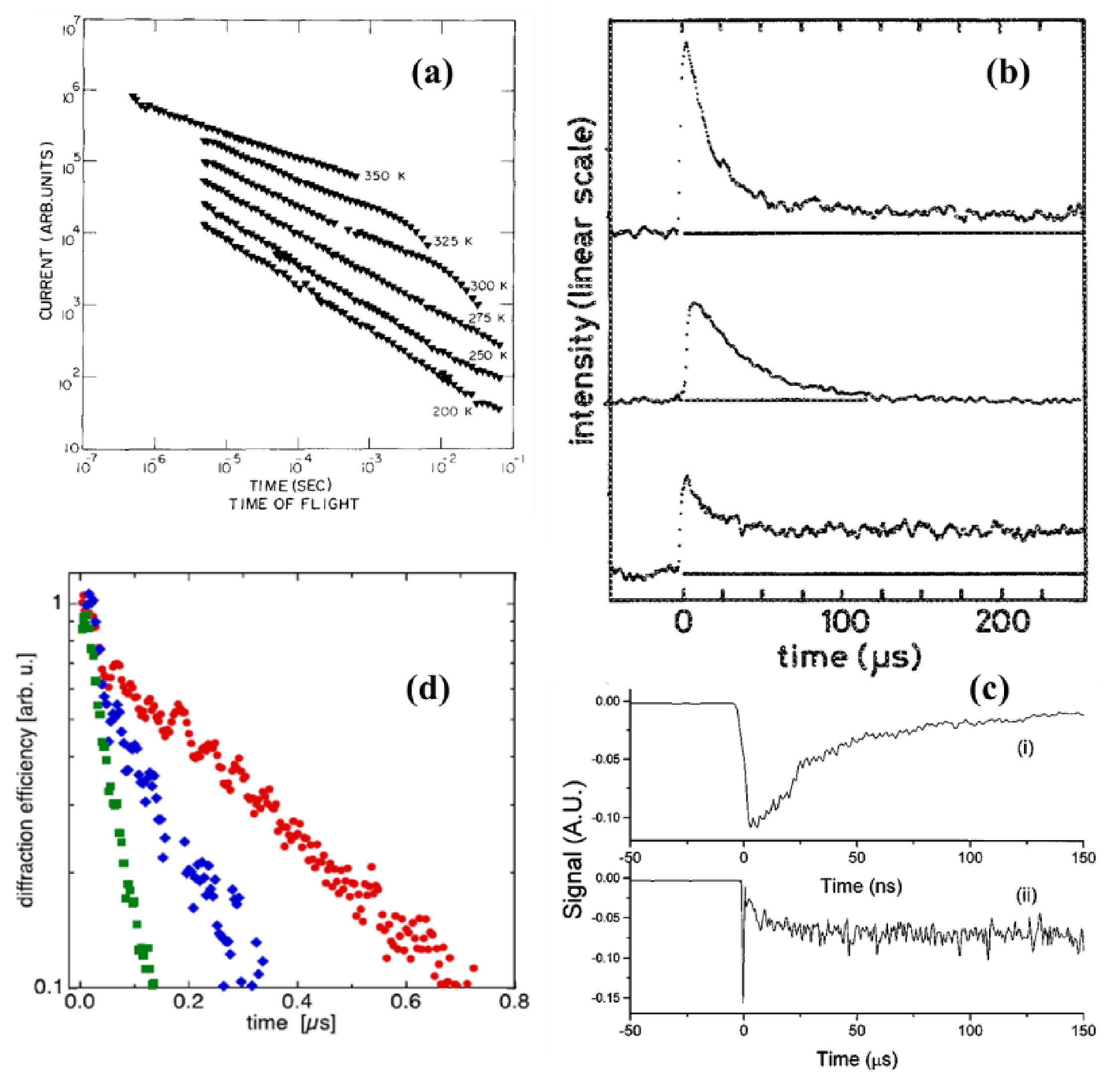
From the CW optical pump-probe studies on PD/PB discussed above, we learned that such effect consists of two parts: metastable PD/PB and transient PD (TPD). As shown earlier, any sample exhibits TPD only during illumination [18,40]. Interestingly, it has been shown that for short illumination with a CW light, the transient part is more apparent than the slow and cumulative metastable part. However, most of the previous studies on transient effects were performed with CW laser, which has very low time resolution, and consequently, an exact assessment of these effects remains rather unknown. In ChGs, time-of-flight (TOF) experiments emerged as a pioneering technique to study light-induced effects [50,51,52]. TOF measurements are based on measuring the current signal in the external circuit that is generated because of the drift of photocarriers across an applied electric field. First TOF measurements were performed on 1–2 μm thick As2Se3 with nitrogen-laser-pumped dye laser of wavelength 483 nm with a pulse duration of 10 ns [51], as shown in Figure 8a. TOF measurements performed at different temperatures between 200 to 350 K show almost no deviation from the expected power-law characteristics.
In another pioneer work, Tanaka aimed to understand the transient behavior of the photoinduced effects, which appear to be governed by lattice distortions [53]. In his work, Tanaka used As2S3 thin film of thickness 1 μm and performed transient grating experiments with 488 nm, 5 ns pulsed laser to understand the time-resolved features of refractive index variation. Time evolution of light-induced effects in annealed As2S3 sample with pulsed and biased CW laser is shown on the top and middle panels of Figure 8b, respectively. For pulsed laser, the effect is irreversible as it does not decay to zero unlike CW; therefore, it can be exploited for optical memory devices. For the experiments performed at 80 K (bottom panel) with pulsed laser, it exhibits less effect with much slower time response since the bandgap becomes wider with decreasing temperature and, likewise, absorption becomes smaller.
Similar to the work of Tanaka, Rosenblum and co-workers [54] tried to understand the dynamic as well as the after-pulse effect in 0.3–1 μm thick As50Se50 thin films by performing transient grating experiments using 532 nm, 5 ns, neodymium-doped yttrium aluminum garnet (Nd:YAG) laser. A dual time behavior is observed the faster component, i.e., the transient effect takes place in tens of nanoseconds, which are followed by an asymptotically decayed slower component in the order of microseconds (Figure 8c). Interestingly, the transient component scales a linear relationship with laser intensity, whereas the after pulsed effect varies quadratically with the laser intensity, which indicates a nonlinear two-photon process associated with ChGs.
Much later in 2012, Regmi and colleagues performed pump-probe transient grating experiments in As2Se3 thin films of thickness 100–200 nm, with 532 nm laser, 20 ps laser [55]. The main difference between their work and earlier studies discussed above is that they pre-illuminated the sample, with a laser having wavelength close to the bandgap of the sample to make it permanently photodarkened. Likewise, they cancel any permanent photoinduced change and focus only on nanosecond dynamics originating from short-lived excited states. In this regard, Figure 8d depicts the time dependence of the diffraction efficiency that decays exponentially on the sub-microsecond time scale. The time constant consists of two parts, excitonic lifetime and diffusion time, which are separated by changing transport length by varying the angle between the interfering beams. They experimentally demonstrated mobility that is 5 orders of magnitude larger than typical TOF mobilities [52].
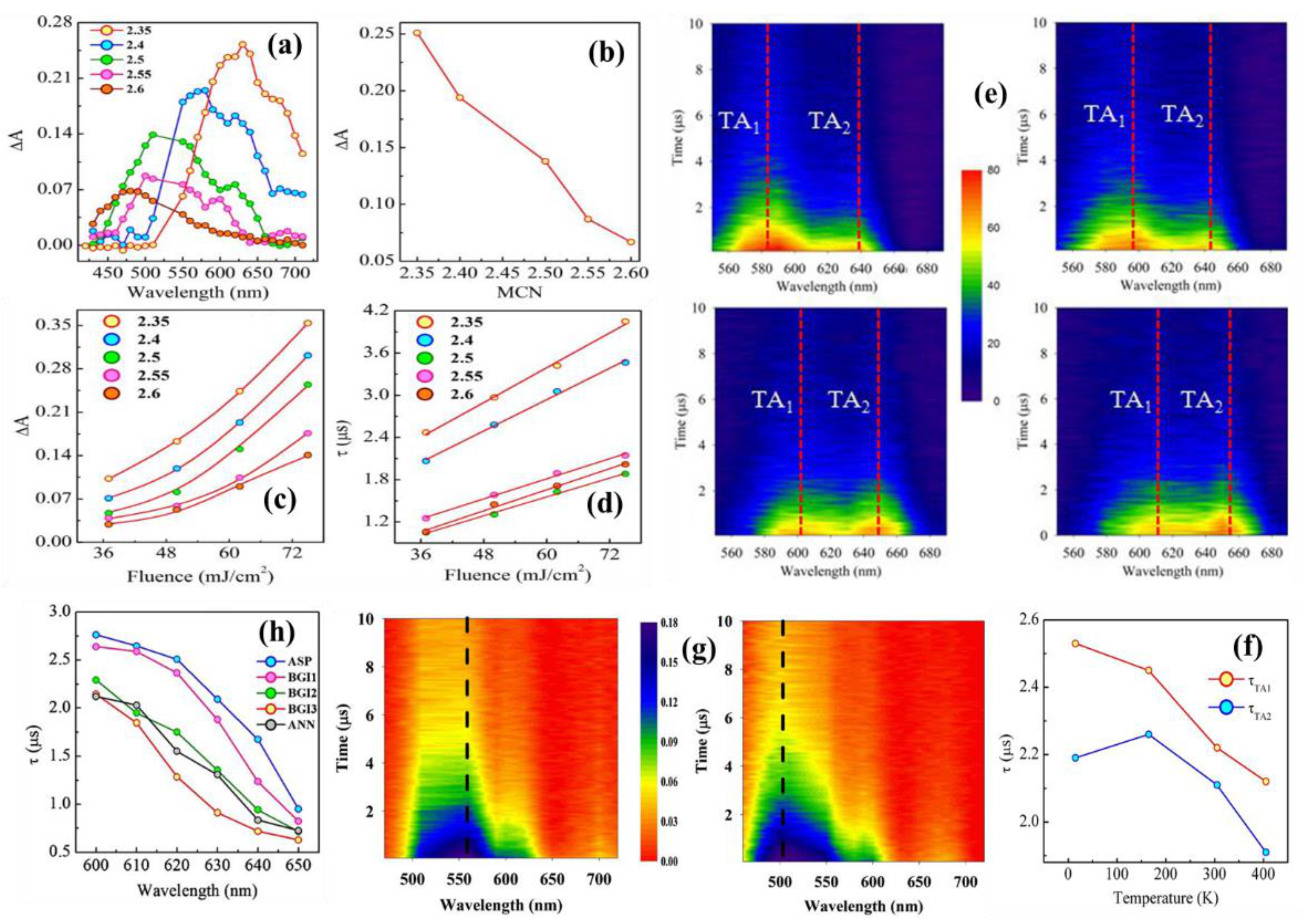
Till now, in all the above-mentioned experiments, the transient photoinduced effects are probed at fixed wavelengths, and therefore information of such effects over a broadband absorption spectrum remains unknown for ns laser excitation. Likewise, although the effects of measuring temperature and excitation fluence are well established for CW illumination [18,40], their effects remain unexplored for ns laser. In our previous work in a-GexAs35-xSe65 thin films of average thickness of 1 μm, we attempted to address such issues by performing TA measurements with 5 ns, 532 nm laser [16]. In this regard, Figure 9a depicts the absorbance change (), i.e., TA for six samples with varying MCN from 2.35 to 2.6 at fixed probe delay of 200 ns. Here, we defined = −log(es/gs), where es is time dependent transmitted intensity of probe pulse in the excited state after pump excitation and gs is the transmitted intensity of probe pulses in the ground state, respectively. It can be seen that TA spectra are compositionally tunable as it blueshifts with increase in x and MCN.
However, most importantly, the magnitude of TA decreases dramatically with increasing MCN (Figure 9b), i.e., by moving from floppy to rigid network as proposed by Phillips and Thorpe [37,38]. This observation provides the first direct experimental validation of the network for ns pulsed illumination. We also validate the two-photon effect proposed by Rosenblum [54] by performing an excitation fluence-dependent TA study, as shown in Figure 9c. With the increase in excitation fluence, TA maxima increase non-linearly, which fits very well with a second-order polynomial equation that confirms that TA is originated from the two-photon process. This observation also fuels the idea of Lucas that irradiation with higher excitation fluence could induce adequate bond breaking or rearrangement to produce appreciable ΔA even in over-coordinated glasses (orange circles), as evident from the figure. Excitation fluence also affects the TA kinetics, which is addressed by fitting single wavelength kinetics at TA maxima with one decay constant, τ. Figure 9d shows that τ increases linearly with excitation fluence, i.e., TA kinetics is faster at lower fluence. This behavior is expected since at higher excitation fluence, permanent structural changes take place that makes the relaxation process significantly slower.
We have already discussed the influence of temperature on CW light-induced effects in terms of magnitude and kinetics of PD and PB [32,43]. Similar temperature dependence on the ns light-induced effect is also studied by our group in Ge5As30Se65 thin films [56]. The 2-dimensional (2D) contour plot of TA spectra at 15, 165, 300, and 405 K is shown in Figure 9e. Clearly, at all temperatures of illumination, two discrete absorption bands, TA1 and TA2, are observed. The observation of dual TA bands is in stark contrast to the small polaron model [57] that predicts a broad featureless absorption spectrum. Following pump excitation, ΔA rises instantaneously and decays within 10 μs; however, complete decay is not observed within the limit of experimental time delay. Notably, both TA1 and TA2 bands are thermally tunable since these bands are redshifted from 582 to 610 nm and 638 to 657 nm, respectively, when the temperature is raised from 15 to 405 K. Interestingly, TA1 and TA2 exhibit contrasting behavior with respect to temperature, i.e., while TA1 decreases, TA2 increases with temperature. At low and room temperatures, TA1 dominates over TA2; however, at high temperature (405 K), TA2 plays the predominant role. Nonetheless, the overall magnitude of TA, by taking contributions from both TA1 and TA2, is found to be the largest at low temperatures. Temperature also has a significant effect on TA kinetics. From Figure 9f, both TA1 (τ1) and TA2 (τ2) decrease with increase in temperature, manifesting that the relaxation process becomes more rapid at higher temperatures, i.e., the relaxation of TA is a thermally activated process which indicates the transient defect states associated with it relaxes immediately at high temperature with the aid of thermal vibration. Similar temperature dependence is also obtained for As2S3 thin films for both 532 and 355 nm, 5ns laser excitation [58].
Controlling and tuning ns light-induced effects is a very challenging problem that can be done very efficiently with background illumination (BGI) since we already knew that CW light can significantly modify the structure of the ChGs to control the final state, whether darkened or bleached. In this regard, we have illuminated the 1 μm thick Ge25As10Se65 thin films continuously for nearly 2 h with a 532 nm CW laser until the sample gets completely photobleached. After, we record the ns TA in as-prepared (ASP) and BGI samples, as shown in Figure 9g [59]. Strikingly, although the magnitude of TA remains the same, most importantly TA spectra of the BGI sample dramatically blue shift from 560 nm to 500 nm compared to the ASP sample. We also found that the blueshift increases linearly with the intensity of the CW illumination. Kinetically, τ is found to be smaller for the BGI samples compared to ASP ones, i.e., the TA relaxation is faster in the BGI samples (Figure 9h). Apart from that, we learned that, for both ASP and BGI samples, TA at longer wavelengths decay faster than the shorter wavelengths, which reveals that the lifetime of photoexcited carriers’ deep traps is longer than in shallow traps [58].
4. Ultrafast Light-Induced Effects in ChGs
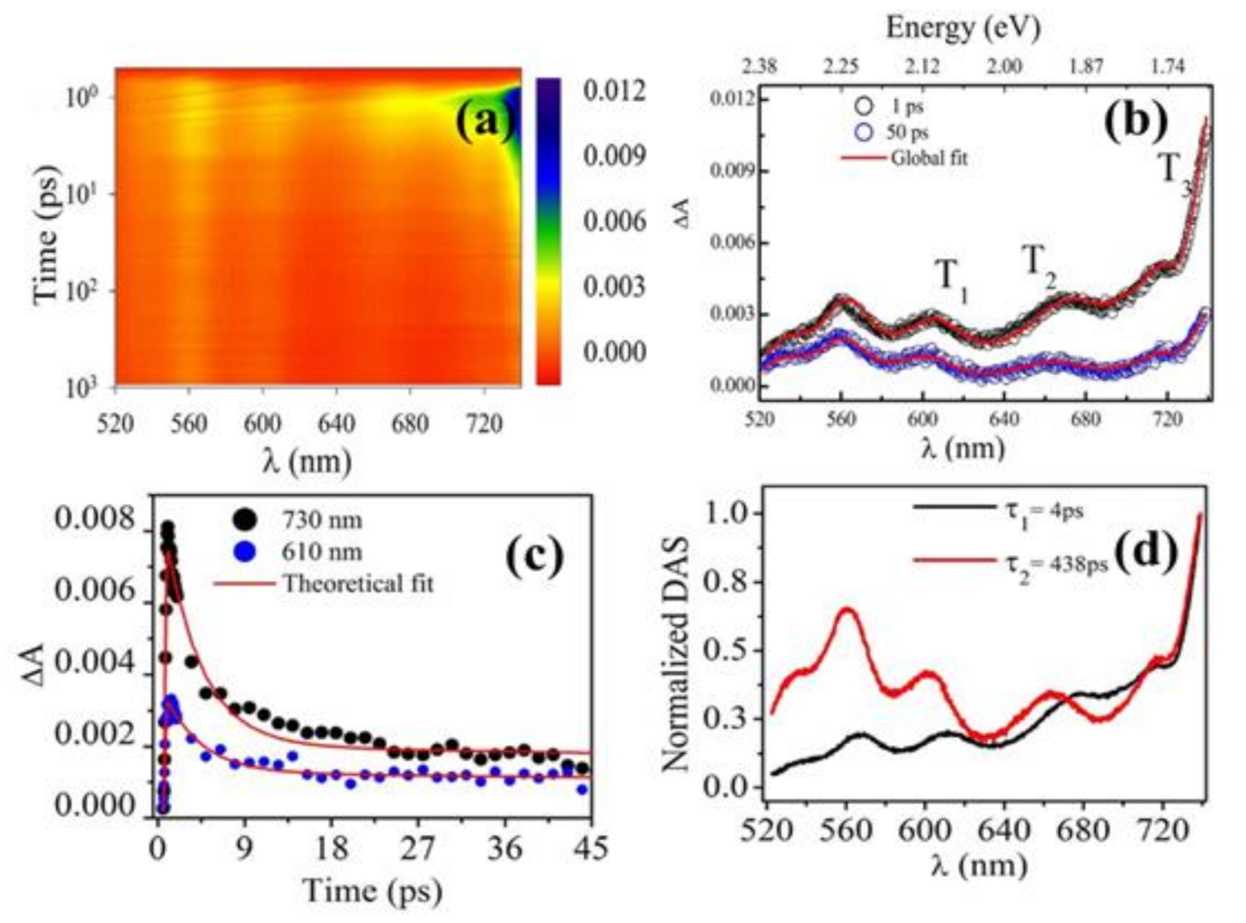
Femtosecond (fs) laser illuminated ultrafast light-induced effects in ChGs thin films are scarce until it was first demonstrated earlier by our group in GeSe2 thin films of thickness 1 μm [15]. The motivation is intrigued from the first principle molecular dynamic simulations [60] that shows light-induced structural changes through defects occur at short (<500 fs) to long timescales (>500 fs) through the creating and annihilation of intimate valence alteration pairs (IVAPs) and VAPs, respectively [61,62]. To probe ultrafast light-induced effects GeSe2 thin films are excited with 100 fs, 400 nm and recorded the TA between 520–740 nm probe wavelength as shown in the 2D contour plot of Figure 10a [15]. Several cross-sections of the contour at different probe delays are depicted in Figure 10b. Important features consist of 3 TA bands (T1, T2, and T3), long-lived probe delays are shown in Figure 10b. T1 and T2 and a short-lived T3. T1 and T2 occur at 650 and 610 nm respectively, from the VAPs. On the other hand, T3 takes place between IVAPs at 725 nm.
Since IVAPs are closely spaced they can self-annihilate easily, thus makes the kinetics faster. To get a detailed analysis of the kinetics of ultrafast TA, global fitting by wavelength-dependent decay associated spectra (DAS(λ)) is employed. In this regard, Figure 10c depicts the temporal evolution of TA kinetics at the selected probe wavelength of 610 and 730 nm, associated with VAP and IVAP, respectively. Two decay constants are obtained with DAS1 (fast) and DAS2 (slow) associated with τ1= 4 ps and τ2= 438 ps. As shown in Figure 10d DAS1 dominates at longer wavelength, while DAS2 is dominant at shorter wavelength.
We have seen earlier that ns TA in GexAs35-xSe65 thin films decreases from floppy to rigid networks in accordance with network rigidity theory [37,38]. To prove the validity of the theory under ultrafast pulsed excitation, we performed femtosecond pump-probe measurements in GexAs35-xSe65 thin films of thickness 700 nm with 400 nm, 120 fs laser, and the TA data for the samples are shown in Figure 11a at probe delay of 1 ps [63]. TA decreases when MCN increases from 2.4 to 2.6; however, interestingly, even beyond the rigidity percolation threshold, the sample with MCN = 2.6 shows significant TA, which was not predicted by network rigidity theory. In fact, with the increase in excitation fluence, we could observe a manifold increase in the amplitude of TA for MCN = 2.6 as well as for other samples in a linear fashion, as shown in Figure 11b. Since Figure 11a demonstrates that TA decay rates are different in different regions of the spectra, it calls for global DAS analysis over a broadband wavelength regime. In this regard, Figure 11c,d show the kinetics of DAS1 and DAS2 (640 nm), from the sub-bandgap (690–720 nm) and bandgap (600–640 nm) region, respectively. DAS1 in the sub-bandgap region for all samples within 10s of picosecond (ps), which is associated with electron-lattice interaction. From Figure 11c, we found that the DAS1 curve is indistinguishable for MCN 2.5 and 2.6 but least steep for MCN 2.4, which tells us that electron-lattice interaction becomes slower in a lightly constrained network compared to over-constrained ones. In stark contrast, DAS2 is slower than DAS1 and occurs over a few hundred ps; it becomes steeper while transitioning from ⟨⟩ = 2.40 to 2.60. Such an observation indicates that exciton recombination and associated structural changes become faster in over-constrained networks compared to lightly constrained ones thanks to the strong restoring forces of the rigid network. Numerically, τ2 corresponding to DAS2 is found to be 417 ± 3, 355 ± 3, 271 ± 3, and 151 ± 2 ps for MCN 2.4, 2.45, 2.5, and 2.6, respectively.
Apart from Ge-As-Se, Ge-Sb-Te (GST) also requires special mention because of their application as a phase change material [64,65,66]. The first observation of phase change in GST was first reported by Konishi and co-workers [64]. They performed ultrafast pump-probe reflectivity measurements in 20 nm thick GST film, and the results are shown in Figure 12a for different pump fluences. Following pump excitation, reflectivity decreases immediately within 500 fs, which either decreased further or recovered depending on the strength of the pump beam. The phase change is evinced from the decrease in reflectivity. For 12.8 mJ/cm2, reflectivity slowly recovered at long probe delays; for 16.6 mJ/cm2, reflectivity recovered slightly after initial rapid decreases; however, for 18.1 mJ/cm2, it never recovers and decrease further in longer probe delays. Clearly, the higher the laser dose, the stronger the amorphization. In another work, Takeda et al. [65] studied the irreversible ultrafast crystalline-to-amorphous phase transition in 10 nm GST ChGs alloy thin film with 100 fs, 800 nm laser by employing broadband single-shot imaging spectroscopy. In this regard, Figure 12b depicts the 2D contour plot of absorption with wavelength and time for a laser fluence 26.3 mJ/ cm2. A rapid change in irreversible absorbance is observed that demonstrates the transition from crystalline to amorphous phase. A more consistent picture of phase change is depicted in Figure 12c, which shows the ultrafast temporal evolution of absorbance against the pump fluence. Absorption changes rapidly at all fluence within 1 ps. Below 6.6 mJ/cm2, absorption recovers; however, for fluence higher than 8.8 mJ/cm2, absorption change is permanent, which demonstrates the irreversible crystalline to amorphous phase change in GST material.
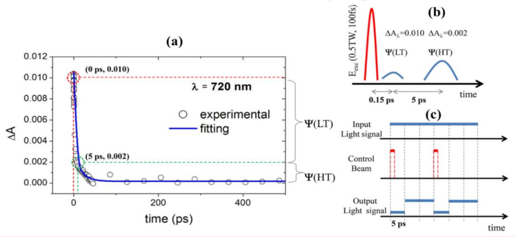
Ultrafast light-induced effects have, in a-Se/Ag bilayer ChGs of thickness 500 nm (Se 450 nm and Ag 50 nm), found tremendous potential application thanks to the formation of spatially ordered and interconnected Ag nanoparticles (AgNPs) on the surface of Se through optically driven diffusion [67]. The AgNP, after the formation, interacts with intense femtosecond laser pulses and provides an ultrafast optical response that can be exploited for application. In this regard, Figure 13a shows the time evolution of kinetics curves of AgNP on Se at 720 nm. The TA decays to 20% of the maximum within a time period of 5 ps. By defining maximum absorbance as high transmission (HT) and 20% absorbance as low transmission (LT), the response can be utilized to make an optical switching device between HT to LT with a switching speed of 5 ps (Figure 13b). As an example, a schematic of an optical modulator is shown in Figure 13c in which the control pump beam modulates the transmission of the signal probe beam. The ultrafast exciton-plasmon coupling has also been exploited to explore new functionalities in plasmon/ChGs heterostructures which are unachievable by individual components [68].
5. Conclusions
The present review covers two contrasting important aspects of light-induced effects in chalcogenide glasses (ChGs) separated by the pulse-duration of the excitation laser. In the first part, photodarkening (PD) and photobleaching (PB) which take place under continuous wave (CW) illumination through homopolar to heteropolar bond conversion and are predominantly metastable with a negligible transient component are discussed. It was showed that by tuning the chemical composition of the individual components, PD and PB can be tuned. Moreover, PD is found to be dominant at lower and room temperatures, while PB dominates at high temperatures through photo-oxidation. In the second part, transient absorption (TA) is discussed under pulsed laser illumination that takes place via exciton self-trapping. Importantly, unlike CW illumination, for pulsed laser, light-induced effects decrease from floppy to rigid network in accordance with network rigidity theory. Apart from that, several studies show that TA can be spectrally tunable with the temperature of illumination as well as via background CW illumination.
Funding
This research was funded by Science and Engineering Research Board (Project No. EMR/2016/002520), Council of Scientific and Industrial Research, India (Grant No. 03 (1250)/12/EMR-II), and DAE BRNS (Sanction No. 37(3)/ 14/26/2016-BRNS/37245).
Conflicts of Interest
The authors declare no conflict of interest.
References
- Shimakawa, K.; Kolobov, A.; Elliott, S. Photoinduced effects and metastability in amorphous semiconductors and insulators. Adv. Phys. 1995, 44, 475–588. [Google Scholar] [CrossRef]
- Sharma, P.; Sharma, N.; Sharda, S.; Katyal, S.; Sharma, V. Recent developments on the optical properties of thin films of chalcogenide glasses. Prog. Solid State Chem. 2016, 44, 131–141. [Google Scholar] [CrossRef]
- Bureau, B.; Zhang, X.H.; Smektala, F.; Adam, J.-L.; Troles, J.; Ma, H.-L.; Boussard-Plèdel, C.; Lucas, J.; Lucas, P.; Le Coq, D.; et al. Recent advances in chalcogenide glasses. J. Non-Cryst. Solids 2004, 345–346, 276–283. [Google Scholar] [CrossRef]
- Watts, R.K.; De Wit, M.; Holton, W.C. Nonoxide Chalcogenide Glass Films for Integrated Optics. Appl. Opt. 1974, 13, 2329–2332. [Google Scholar] [CrossRef] [PubMed]
- Bureau, B.; Boussard, C.; Cui, S.; Chahal, R.; Anne, M.L.; Nazabal, V.; Sire, O.; Loréal, O.; Lucas, P.; Monbet, V.; et al. Chalcogenide optical fibers for mid-infrared sensing. Opt. Eng. 2014, 53, 27101. [Google Scholar] [CrossRef]
- Calvez, L.; Yang, Z.; Lucas, P. Composition dependence and reversibility of photoinduced refractive index changes in chalcogenide glass. J. Phys. D Appl. Phys. 2010, 43, 445401. [Google Scholar] [CrossRef]
- Khan, P.; Bhattacharya, A.; Joshy, A.; Sathe, V.; Deshpande, U.; Adarsh, K. Investigation of temperature dependent optical modes in Ge x As 35−x Se 65 thin films: Structure specific Raman, FIR and optical absorption spectroscopy. Thin Solid Films 2017, 621, 76–83. [Google Scholar] [CrossRef] [Green Version]
- Eggleton, B.J.; Luther-Davies, B.; Richardson, K. Chalcogenide photonics. Nat. Photon. 2011, 5, 141–148. [Google Scholar] [CrossRef]
- Street, R. Non-radiative recombination in chalcogenide glasses. Solid State Commun. 1977, 24, 363–365. [Google Scholar] [CrossRef]
- Street, R.A. Recombination in a-Si: H: Spin-dependent effects. Phys. Rev. B 1982, 26, 3588–3604. [Google Scholar] [CrossRef]
- Halpern, V. On the photoconductivity of amorphous chalcogenide semiconductors. Philos. Mag. B 1978, 37, 423–434. [Google Scholar] [CrossRef]
- Kastner, M.; Adler, D.; Fritzsche, H. Valence-Alternation Model for Localized Gap States in Lone-Pair Semiconductors. Phys. Rev. Lett. 1976, 37, 1504–1507. [Google Scholar] [CrossRef]
- Ganjoo, A.; Jain, H. Millisecond kinetics of photoinduced changes in the optical parameters ofa−As2S3films. Phys. Rev. B 2006, 74, 024201. [Google Scholar] [CrossRef]
- Ganjoo, A.; Shimakawa, K.; Kitano, K.; Davis, E. Transient photodarkening in amorphous chalcogenides. J. Non-Cryst. Solids 2002, 299–302, 917–923. [Google Scholar] [CrossRef]
- Barik, A.R.; Bapna, M.; Drabold, D.A.; Adarsh, K.V. Ultrafast light induced unusually broad transient absorption in the sub-bandgap region of GeSe2 thin film. Sci. Rep. 2014, 4, 3686. [Google Scholar] [CrossRef] [Green Version]
- Khan, P.; Saxena, T.; Adarsh, K.V. Tailoring between network rigidity and nanosecond transient absorption in a-Ge_xAs_35-xSe_65 thin films. Opt. Lett. 2015, 40, 768–771. [Google Scholar] [CrossRef] [Green Version]
- Berkes, J.S.; Ing, S.W.; Hillegas, W.J. Photodecomposition of Amorphous As2Se3 and As2S3. J. Appl. Phys. 1971, 42, 4908–4916. [Google Scholar] [CrossRef]
- Khan, P.; Barik, A.R.; Vinod, E.M.; Sangunni, K.S.; Jain, H.; Adarsh, K.V. Coexistence of fast photodarkening and slow photobleaching in Ge19As21Se60 thin films. Opt. Express 2012, 20, 12416–12421. [Google Scholar] [CrossRef] [Green Version]
- Yang, G.; Jain, H.; Ganjoo, A.; Zhao, D.; Xu, Y.; Zeng, H.; Chen, G. A photo-stable chalcogenide glass. Opt. Express 2008, 16, 10565–10571. [Google Scholar] [CrossRef]
- Antoine, K.; Jain, H.; Vlcek, M.; Senanayake, S.D.; Drabold, D.A. Chemical origin of polarization-dependent photoinduced changes in anAs36Se64glass film viain situsynchrotron x-ray photoelectron spectroscopy. Phys. Rev. B 2009, 79, 054204. [Google Scholar] [CrossRef] [Green Version]
- Lyubin, V.; Klebanov, M.; Bruner, A.; Shitrit, N.; Sfez, B. Transient photodarkening and photobleaching in glassy GeSe2 films. Opt. Mater. 2011, 33, 949–952. [Google Scholar] [CrossRef]
- Yan, Q.; Jain, H.; Ren, J.; Zhao, D.; Chen, G. Effect of Photo-Oxidation on Photobleaching of GeSe2 and Ge2Se3 Films. J. Phys. Chem. C 2011, 115, 21390–21395. [Google Scholar] [CrossRef]
- Spence, C.A.; Elliott, S.R. Light-induced oxidation and band-edge shifts in thermally evaporated films of germanium chalcogenide glasses. Phys. Rev. B 1989, 39, 5452–5463. [Google Scholar] [CrossRef] [PubMed]
- Tichý, L.; Tichá, H.; Nagels, P.; Sleeckx, E. A review of the specific role of oxygen in irreversible photo- and thermally induced changes of the optical properties of thin film amorphous chalcogenides. Opt. Mater. 1995, 4, 771–779. [Google Scholar] [CrossRef]
- Mori, T.; Hosokawa, N.; Shimakawa, K. Dynamics of photodarkening in amorphous As2Se3 films: In Situ simultaneous measurements of optical transmittance and photocurrent. J. Non-Cryst. Solids 2008, 354, 2683–2686. [Google Scholar] [CrossRef]
- Sati, D.C.; Kumar, R.; Mehra, R.M.; Jain, H.; Ganjoo, A. Kinetics of photodarkening in a-As2Se3 thin films. J. Appl. Phys. 2009, 105, 123105. [Google Scholar] [CrossRef]
- Van Popta, A.C.; DeCorby, R.G.; Haugen, C.J.; Robinson, T.; McMullin, J.N.; Tonchev, D.; Kasap, S.O. Photoinduced refractive index change in As2Se3 by 633nm illumination. Opt. Express 2002, 10, 639–644. [Google Scholar] [CrossRef]
- Swanepoel, R. Determination of the thickness and optical constants of amorphous silicon. J. Phys. E Sci. Instrum. 1983, 16, 1214–1222. [Google Scholar] [CrossRef]
- Kronig, R.D.L. On the Theory of Dispersion of X-Rays. J. Opt. Soc. Am. 1926, 12, 547–557. [Google Scholar] [CrossRef]
- Barik, A.R.; Naik, R.; Adarsh, K. Unusual observation of fast photodarkening and slow photobleaching in a-GeSe2 thin film. J. Non-Cryst. Solids 2013, 377, 179–181. [Google Scholar] [CrossRef]
- Liu, Y.; Jain, H.; Ren, J.; Yan, Q.; Chen, G. High-Resolution X-ray Photoelectron Spectroscopy Study of Photo-Oxidation of Amorphous Oxy-Chalcogenide Films. J. Phys. Chem. C 2012, 116, 24590–24595. [Google Scholar] [CrossRef]
- Khan, P.; Sharma, R.; Deshpande, U.; Adarsh, K.V. First observation of the temperature-dependent light-induced response of Ge(25)As(10)Se(65) thin films. Opt. Lett. 2015, 40, 1559–1562. [Google Scholar] [CrossRef] [Green Version]
- Zhang, S.; Chen, Y.; Wang, R.; Shen, X.; Dai, S. Observation of photobleaching in Ge-deficient Ge16.8Se83.2 chalcogenide thin film with prolonged irradiation. Sci. Rep. 2017, 7, 14585. [Google Scholar] [CrossRef] [Green Version]
- Kumar, R.R.; Barik, A.R.; Vinod, E.M.; Bapna, M.; Sangunni, K.S.; Adarsh, K.V. Crossover from photodarkening to photobleaching in a-Ge_xSe_100-x thin films. Opt. Lett. 2013, 38, 1682–1684. [Google Scholar] [CrossRef]
- Calvez, L.; Yang, Z.; Lucas, P. Light-Induced Matrix Softening of Ge-As-Se Network Glasses. Phys. Rev. Lett. 2008, 101, 177402. [Google Scholar] [CrossRef]
- Wang, R.P.; Bulla, D.; Smith, A.; Wang, T.; Luther-Davies, B. Structure and physical properties of Ge[sub x]As[sub y]Se[sub 1−x−y] glasses with the same mean coordination number of 2.5. J. Appl. Phys. 2011, 109, 23517. [Google Scholar] [CrossRef] [Green Version]
- Phillips, J. Topology of covalent non-crystalline solids I: Short-range order in chalcogenide alloys. J. Non-Cryst. Solids 1979, 34, 153–181. [Google Scholar] [CrossRef]
- Thorpe, M. Continuous deformations in random networks. J. Non-Cryst. Solids 1983, 57, 355–370. [Google Scholar] [CrossRef]
- Lucas, P. Energy landscape and photoinduced structural changes in chalcogenide glasses. J. Phys. Condens. Matter 2006, 18, 5629–5638. [Google Scholar] [CrossRef]
- Khan, P.; Jain, H.; Adarsh, K.V. Role of Ge:As ratio in controlling the light-induced response of a-GexAs35−xSe65 thin films. Sci. Rep. 2014, 4, 4029. [Google Scholar] [CrossRef] [Green Version]
- Zhang, Z.; Xu, S.; Chen, Y.; Shen, X.; Wang, R. Photo-induced effects in Ge-As-Se films in various states. Opt. Mater. Express 2020, 10, 540. [Google Scholar] [CrossRef]
- Němec, P.; Zhang, S.; Nazabal, V.; Fedus, K.; Boudebs, G.; Moreac, A.; Cathelinaud, M.; Zhang, X.-H. Photo-stability of pulsed laser deposited Ge_xAs_ySe_100-x-y amorphous thin films. Opt. Express 2010, 18, 22944–22957. [Google Scholar] [CrossRef]
- Khan, P.; Joshy, A.; Bhattacharya, A.; Adarsh, K. Observation of giant photodarkening and temperature mediated transition to photobleaching in As2Se3/Ag/Se trilayer. J. Non-Cryst. Solids 2016, 449, 70–74. [Google Scholar] [CrossRef]
- Mitkova, M.; Kozicki, M. Ag-photodoping in Ge-chalcogenide amorphous thin films—Reaction products and their characterization. J. Phys. Chem. Solids 2007, 68, 866–872. [Google Scholar] [CrossRef]
- Wagner, T.; Ewen, P. Photo-induced dissolution effect in Ag/As33S67 multilayer structures and its potential application. J. Non-Cryst. Solids 2000, 266–269, 979–984. [Google Scholar] [CrossRef]
- Khan, P.; Xu, Y.; Leon, W.; Adarsh, K.; Vezenov, D.; Biaggio, I.; Jain, H. Kinetics of photo-dissolution within Ag/As2S3 heterostructure. J. Non-Cryst. Solids 2018, 500, 468–474. [Google Scholar] [CrossRef] [Green Version]
- Palumbo, V.P.; Kovalskiy, A.; Jain, H.; Huey, B.D. Direct investigation of silver photodissolution dynamics and reversibility in arsenic trisulphide thin films by atomic force microscopy. Nanotechnology 2013, 24, 125706. [Google Scholar] [CrossRef] [PubMed]
- Binu, S.; Khan, P.; Barik, A.R.; Sharma, R.; Golovchak, R.; Jain, H.C.; Adarsh, K.V. Photoinduced formation of Ag nanoparticles on the surface of As2S3/Ag thin bilayer. Mater. Res. Express 2014, 1, 045025. [Google Scholar] [CrossRef]
- Kolobov, A.V.; Elliott, S.R. Photodoping of amorphous chalcogenides by metals. Adv. Phys. 1991, 40, 625–684. [Google Scholar] [CrossRef]
- Pfister, G.; Scher, H. Dispersive (non-Gaussian) transient transport in disordered solids. Adv. Phys. 1978, 27, 747–798. [Google Scholar] [CrossRef]
- Khan, B.A.; Kastner, M.A.; Adler, D. Time-of-flight and photoconductivity studies of a-As2Se3 films. Solid State Commun. 1983, 45, 187–189. [Google Scholar] [CrossRef]
- Owen, A.; Robertson, J. Electronic properties of some simple chalcogenide glasses. J. Non-Cryst. Solids 1970, 2, 40–51. [Google Scholar] [CrossRef]
- Tanaka, K. Transient-grating study of amorphous As2S3 films. J. Appl. Phys. 1989, 65, 2042–2046. [Google Scholar] [CrossRef]
- Rosenblum, G.; Sfez, B.G.; Kotler, Z.; Lyubin, V.; Klebanov, M. Nonlinear optical effects in chalcogenide photoresists. Appl. Phys. Lett. 1999, 75, 3249–3251. [Google Scholar] [CrossRef]
- Regmi, A.; Ganjoo, A.; Zhao, D.; Jain, H.; Biaggio, I. Fast excited state diffusion in a-As2Se3 chalcogenide films. Appl. Phys. Lett. 2012, 101, 61911. [Google Scholar] [CrossRef]
- Khan, P.; Saxena, T.; Jain, H.; Adarsh, K.V. Nanosecond light induced, thermally tunable transient dual absorption bands in a-Ge5As30Se65 thin film. Sci. Rep. 2014, 4, 6573. [Google Scholar] [CrossRef] [Green Version]
- Emin, D. Dynamics of the optically induced properties of a small-polaronic glass. J. Non-Cryst. Solids 1980, 35–36, 969–973. [Google Scholar] [CrossRef] [Green Version]
- Khan, P.; Acharja, P.; Joshy, A.; Bhattacharya, A.; Kumar, D.; Adarsh, K. Nanosecond light-induced transient absorption in As2S3: Self-trapped exciton recombination in amorphous chalcogenides. J. Non-Cryst. Solids 2015, 426, 72–77. [Google Scholar] [CrossRef]
- Khan, P.; Yadav, R.K.; Bhattacharya, A.; Joshy, A.; Aneesh, J.; Adarsh, K.V. Tuning nanosecond transient absorption in a-Ge_25As_10Se_65 thin films via background illumination. Opt. Lett. 2015, 40, 4512. [Google Scholar] [CrossRef]
- Li, J.; Drabold, D. Direct Calculation of Light-Induced Structural Change and Diffusive Motion in Glassy As2Se3. Phys. Rev. Lett. 2000, 85, 2785–2788. [Google Scholar] [CrossRef] [Green Version]
- Zhang, X.; Drabold, D.A. Direct Molecular Dynamic Simulation of Light-Induced Structural Change in Amorphous Selenium. Phys. Rev. Lett. 1999, 83, 5042–5045. [Google Scholar] [CrossRef] [Green Version]
- Zhang, X.; Drabold, D.A. Simul. of the response of amorphous selenium to light. Int. J. Mod. Phys. B 2001, 15, 3190–3196. [Google Scholar] [CrossRef]
- Khan, P.; Yadav, R.K.; Adarsh, K.V. Ultrafast light-induced softening of chalcogenide thin films above the rigidity percolation transition. J. Appl. Phys. 2018, 124, 125702. [Google Scholar] [CrossRef] [Green Version]
- Konishi, M.; Santo, H.; Hongo, Y.; Tajima, K.; Hosoi, M.; Saiki, T. Ultrafast amorphization in Ge_10Sb_2Te_13 thin film induced by single femtosecond laser pulse. Appl. Opt. 2010, 49, 3470–3473. [Google Scholar] [CrossRef]
- Takeda, J.; Oba, W.; Minami, Y.; Saiki, T.; Katayama, I. Ultrafast crystalline-to-amorphous phase transition in Ge2Sb2Te5 chalcogenide alloy thin film using single-shot imaging spectroscopy. Appl. Phys. Lett. 2014, 104, 261903. [Google Scholar] [CrossRef] [Green Version]
- Guo, P.; Sarangan, A.M.; Agha, I. A Review of Germanium-Antimony-Telluride Phase Change Materials for Non-Volatile Memories and Optical Modulators. Appl. Sci. 2019, 9, 530. [Google Scholar] [CrossRef] [Green Version]
- Bapna, M.; Sharma, R.; Barik, A.R.; Khan, P.; Kumar, R.R.; Adarsh, K.V. Light induced diffusion driven self assembly of Ag nanoparticles in a-Se/Ag bi-layer thin film with ultrafast optical response. Appl. Phys. Lett. 2013, 102, 213110. [Google Scholar] [CrossRef]
- Sharma, R.; Khan, P.; Aneesh, J.; Sangunni, K.S.; Csarnovics, I.; Kokenyesi, S.; Jain, H.; Adarsh, K.V. Strong exciton-localized plasmon coupling in a-Ge24Se76/AuNP heterostructure. APL Mater. 2016, 4, 106105. [Google Scholar] [CrossRef]
Figure 1.
(a) Optical transmission spectra of a-As2Se3 thin films for laser intensity of 10 mW/cm2; the red arrow depicts the redshift in in transmission spectra. (b) Time evolution of transmission at 580, 600, and 610 nm for the intensity 10 mW/cm2. All Figures are reprinted with permission from [26] Copyright 2009, American Institute of Physics. (c) Transmission spectra for a-As2S3 films is as-prepared (line), illuminated (at time = 1 s (thick dashes), 60 s (dots), 3600 s (red dash-dots) and post-illuminated (thin dashes)) state. The transmission spectrum is recovered between switch off (blue dash-dots) and switch on (long-short dashes) state of laser illumination. (d) Time evolution of transmission at fixed wavelengths. All Figures are reprinted with permission from [13] Copyright 2006, American Physical Society.

Figure 2.
(a) Time evolution of absorption coefficient at wavelengths between laser ON and OFF states as indicated in the figure. All Figures are reprinted with permission from [13] Copyright 2006, American Physical Society. (b) Change in optical band gap (g) at different laser intensities. The solid black circle depicts g in the as-prepared state before switching on the exciting laser. All Figures are reprinted with permission from [26] Copyright 2009, American Institute of Physics. (c) Time evolution of refractive index (n) at 633 nm during and after illumination. The solid red line denotes the theoretical fit. The solid black circle indicates n in as-prepared state. All Figures are reprinted with permission from [13] Copyright 2006, American Physical Society. (d) Wavelength spectra of refractive index. All Figures are reprinted with permission from [27] Copyright 2002, The Optical Society.

Figure 3.
Transmission spectra of (a) GeSe2 and (b) Ge2Se3 films when illuminated in the air. Time evolution of transmission at fixed wavelengths for as-prepared (c) GeSe2 and (d) Ge2Se3 thin films illuminated in the air. All Figures are reprinted with permission from [22] Copyright 2011, American Chemical Society.

Figure 4.
(a) Infrared (IR) difference (after–before illumination) absorption spectra for GeSe2 (solid line) and Ge2Se3 (dashed line) thin films. All Figures are reprinted with permission from [22] Copyright 2011, American Chemical Society. (b) The difference in transmission kinetics in a-Ge25As10Se65 thin films when illuminated in the vacuum and in air. f and f represent final and initial transmission, respectively. All Figures are reprinted with permission from [32] Copyright 2015, The Optical Society.

Figure 5.
(a) Transmission spectra of Ge16.8Se83.2 thin film in as-prepared and illuminated states at various power densities of 0.02, 0.05, 0.1, 0.2, 0.5, and 1 W/cm2, respectively. Time evolution of f/i when excited with low (b) 0.02 and high (c) 1 W/cm2 power density of the laser. All Figures are reprinted with permission from [33] Copyright 2017, Springer Nature.

Figure 6.
(a) Ge5Se95 and (b) Ge30Se70 thin films in as-prepared (solid black line) and illuminated (solid red line) states when excited with 532 nm laser. Single wavelength kinetics of f/i at 560 nm, when illuminated with 532 nm laser of intensity 0.5 W/ cm2 for (c) Ge5Se95 and (d) Ge30Se70. Here the hollow circles represent the experimental data, while the solid red line indicates theoretical fit.

Figure 7.
(a) Variation of photo expansion and photodarkening (PD) as a function of mean coordination number (MCN) (⟨⟩) in a series of GexAsxSe1-2x network glasses. (b) Comparison of photoinduced and thermally induced enthalpy relaxation in a series of GexAsxSe1-2x glass after illumination with 3 W/cm2 laser until effects are saturated or annealed at 25 °C below g for 80 h until relaxation. All Figures are reprinted with permission from [35] Copyright 2008, American Institute of Physics. (c) Single wavelength kinetics of f/i of all a-GexAs35-xSe65 thin films. The dashed line indicates the time at which the laser was turned on. The transient effects are probed between laser off (downward arrow, wine color) and on (upward arrow, pink color) on states. (d) Schematic diagram used to calculate PD, transient PD (TPD), photobleaching (PB), and cumulative change from the transmission kinetic curve of a-Ge15As20Se65. Quantification of (e) PD and (f) PB against the variation of MCN of the network. MCN increases from 2.4 to 2.6 when x changes from 5 to 25 in a-GexAs35-xSe65 thin films. All Figures are reprinted with permission from [40] Copyright 2014, Springer Nature. (g–i) Temperature-dependent transmission spectra of a-Ge25As10Se65 thin film at 20, 300, and 420 K, respectively, in the as-prepared and post-illuminated states. (j–l) Kinetics of f/i for the wavelength corresponding to as-prepared transmission of 10% at 20, 300, and 420 K, respectively.

Figure 8.
(a) Temperature dependence of time-of-flight (TOF) current transients. All Figures are reprinted with permission from [51] Copyright 1983, Elsevier. (b) Time evolution of diffracted light intensities from grated As2S3 films in the annealed state (top), under bias illumination at room temperature (middle), and in annealed state at 80 K (bottom). All Figures are reprinted with permission from [53] Copyright 1989, American Institute of Physics. (c) The diffracted signal consists of a nanosecond transient (i) component that is followed by a slow asymptotic after-pulse effect (ii). The transient effects are instantaneous with the laser pulse. All Figures are reprinted with permission from [54] Copyright 1999, American Institute of Physics. (d) Temporal evolution of the diffraction efficiency of a photoinduced transient grating in the a-As2Se3 film for three spatial periods of 0.7, 1.1, and 1.6 μm. All Figures are reprinted with permission from [55] Copyright 2012, American Institute of Physics.

Figure 9.
(a) Transient absorption (TA) spectra of a-GexAs35-xSe65 thin films when illuminated with ns pump laser at fixed probe delay of 200 ns. (b) Variation in the amplitude of TA maxima with MCN. (c) Change in TA maximum for samples with different MCN for various excitation fluence, which scales quadratically. (d) Change in decay time constant of TA for samples of different MCN that scales linearly with excitation fluence. Colored symbols represent experimental data, and the solid red lines indicate theoretical fit. (e) 2D contour plot depicting time-resolved TA spectra of a-Ge5As30Se65 thin film at 15, 165, 305, and 405 K when illuminated with 532 nm, 5 ns pulsed laser. (f) Variation of τ1 and τ2, associated with TA1 and TA2 against temperature changes. All Figures are reprinted with permission from [56] Copyright 2014, Springer Nature. (g) 2D contour plot of the TA for as-prepared (ASP) and background illumination (BGI) samples showing spectral and temporal evolution. The vertical dotted lines indicate the TA maxima for both samples. (h) The decay-time constant for ASP and BGI samples at different probe wavelengths shows TA is faster for BGI samples in comparison to ASP samples.

Figure 10.
(a) 2D contour plot of TA spectra of GeSe2 thin film for probe delays in ps time domain. (b) TA spectra at different probe delays at ps time. (c) Temporal evolution of TA at 730 and 610 nm along with theoretical fit (red line). (d) Normalized decay associated spectra (DAS) in ps time delays. All Figures are reprinted with permission from [15] Copyright 2014, Springer Nature.

Figure 11.
(a) TA spectra of a-GexAs35-xSe65 thin films at probe delay of 1 ps when excited with 400 nm pump. (b) Variation of TA maxima in the bandgap region for all samples against laser fluence. Temporal evolution of central wavelengths associated with (c) DAS1 (sub-bandgap region) and (d) DAS2 (bandgap region). All Figures are reprinted with permission from [64] Copyright 2018, American Institute of Physics.

Figure 12.
(a) Change in reflectivity of the probe pulse at different probe delays for fluence of 12.8, 16.6, and 18.1 mJ/cm2, respectively. All Figures are reprinted with permission from [64] Copyright 2014, American Institute of Physics. (b) 2D image of the TA in crystalline Ge-Sb-Te (GST) film for the laser fluence of 26.3 mJ/ cm2. (c) Temporal evolution of the absorbance in crystalline GST film in ps time domain for different laser fluences. All Figures are reprinted with permission from [65] Copyright 2014, American Institute of Physics.

Figure 13.
(a) Ultrafast TA of AgNp/Se bilayer at 720 nm. Hollow circles represent experimental data, and the solid blue line indicates theoretical fit, respectively. Following pump excitation, TA drops to 20% of its maximum value within 5 ps. (b) Schematics showing the effect of the pump (red) on the probe beam (blue). We define a low transmission state Ψ(LT) that corresponds to peak absorption, while 20% of peak absorption is defined as high transmission Ψ(HT) state. (c) Schematic demonstrating the application of the ultrafast response of AgNPs where the output probe transmission can be modulated using a control pump beam. All Figures are reprinted with permission from [67] Copyright 2013, American Institute of Physics.

Publisher’s Note: MDPI stays neutral with regard to jurisdictional claims in published maps and institutional affiliations. |
© 2021 by the authors. Licensee MDPI, Basel, Switzerland. This article is an open access article distributed under the terms and conditions of the Creative Commons Attribution (CC BY) license (https://creativecommons.org/licenses/by/4.0/).
Share and Cite
MDPI and ACS Style
Khan, P.; Adarsh, K.V. Light-Induced Effects in Amorphous Chalcogenide Glasses: Femtoseconds to Seconds. Physics 2021, 3, 255-274. https://0-doi-org.brum.beds.ac.uk/10.3390/physics3020019
AMA Style
Khan P, Adarsh KV. Light-Induced Effects in Amorphous Chalcogenide Glasses: Femtoseconds to Seconds. Physics. 2021; 3(2):255-274. https://0-doi-org.brum.beds.ac.uk/10.3390/physics3020019
Chicago/Turabian StyleKhan, Pritam, and K. V. Adarsh. 2021. "Light-Induced Effects in Amorphous Chalcogenide Glasses: Femtoseconds to Seconds" Physics 3, no. 2: 255-274. https://0-doi-org.brum.beds.ac.uk/10.3390/physics3020019