Avalanche Photodetector Based on InAs/InSb Superlattice


Center for Quantum Devices, Department of Electrical and Computer Engineering, Northwestern University, Evanston, IL 60208, USA
*
Author to whom correspondence should be addressed.
Quantum Rep. 2020, 2(4), 591-599; https://0-doi-org.brum.beds.ac.uk/10.3390/quantum2040041
Submission received: 9 November 2020
/
Revised: 25 November 2020
/
Accepted: 2 December 2020
/
Published: 4 December 2020
(This article belongs to the Special Issue Exclusive Feature Papers of Quantum Reports)
Abstract
:This work demonstrates a mid-wavelength infrared InAs/InSb superlattice avalanche photodiode (APD). The superlattice APD structure was grown by molecular beam epitaxy on GaSb substrate. The device exhibits a 100 % cut-off wavelength of 4.6 µm at 150 K and 4.30 µm at 77 K. At 150 and 77 K, the device responsivity reaches peak values of 2.49 and 2.32 A/W at 3.75 µm under −1.0 V applied bias, respectively. The device reveals an electron dominated avalanching mechanism with a gain value of 6 at 150 K and 7.4 at 77 K which was observed under −6.5 V bias voltage. The gain value was measured at different temperatures and different diode sizes. The electron and hole impact ionization coefficients were calculated and compared to give a better prospect of the performance of the device.
1. Introduction
Detectors with a capability of detecting low photon flux are the major focus for the next generation of mid-wavelength infrared (MWIR) photodetectors. The main application of those detectors is to enhance the identification of a target or an object for astronomical applications or military electro-optical systems for passive/active sensing for MWIR atmospheric transmission windows (3–5 microns). Sensitive MWIR photodetectors also allow for better transmission through common atmospheric problems such as fog, clouds, and smoke with a glance towards applications in free space optical communication [1,2]. MWIR detector material has shown great potential to be utilized for several applications, such as aerial and satellite reconnaissance, target tracking using a heat signal, object identification, vascular and cancer detection, and industrial process monitoring [3,4,5,6,7]. In most of these applications, there is a need to increase the capability of the system to detect light in a low photon flux situation. In this manner, devices with internal gain such as avalanche photodiodes (APDs) can achieve the necessary photon resolution in the situations where only a few photons exist to be detected. MWIR APD devices are suitable for the detection in passive imaging of attenuated optical signals due to long-range applications benefiting from the superior transmission of MWIR light through common atmospheric issues.
For the MWIR APD devices, the HgCdTe material system is a great choice and capable of covering the MWIR spectral range with high gain and low excess noises [8]. So far, HgCdTe is the most mature material system for infrared technology, but it suffers from drawbacks due to bulk and surface instability, lower yields, and higher costs, particularly for fabrication [9,10]. InAs-based APDs have also been reported with acceptable performance but due to a cut-off wavelength limitation, InAs material cannot cover the entire range of the MWIR spectrum [11].
An opportunity exists to introduce a new material capable of low dark current, high quantum efficiency, and single carrier multiplication for use in this MWIR range. Antimony-based III/V materials (bulk and superlattice) are capable of meeting the bandgap requirements for making APDs in the MWIR spectral range. For instance, InSb base APD structures were reported recently to support the capability of this material system [12]. Antimony-based strained layer superlattice (SLS) material is a developing material system benefiting from different aspects of quantum well and device with capabilities to cover the entire range of infrared light. The idea of antimonide-based SLS was first proposed by Nobel Laureate L. Esaki and Sai-Halasz in the 1970s [13]. The superlattice is formed by alternating layers of different constituent material over several periods. The especial band alignment leads to the separation of electrons and holes into the different adjacent layers, respectively. The limited period of SLS structure can enhance the quantum quantization effects causing a transition from a semimetal to a narrow-bandgap semiconductor. This narrow bandgap semiconductor has capability for infrared detection as well as infrared emission. To propose specific superlattice within the infrared spectrum with effective superlattice design, an analytical model can be applied on quantum well structures along with necessary calculations to optimize the thickness of each constituent material inside the superlattice structure. As one of the effective methods, the empirical tight-binding method (ETBM) was implemented to calculate the band structure and cut-off wavelength of the superlattice structure [14]. The type II staggered gap band alignment of the superlattice structure was able to deliver excellent infrared detection with its flexible band structure engineering capabilities using different combinations and compositions of Antimony-based structures such as InAs/GaSb/AlSb or InAs/InAsSb [15,16,17,18,19]. So far, several designs based on superlattice structure were implemented for different types of high gain devices [20,21,22,23]. In this letter we demonstrate a MWIR APD device based on InAs/InSb superlattice. The device is a homojunction structure grown on GaSb substrate. The MWIR APD is a p-i-n device with a capability of internally amplifying charge carriers with an avalanche process under a high reverse bias that can cause impact ionization. The absorbing region of the structure extends the operating wavelength across the MWIR spectral range with the gain of 6 at 150 K. The purpose of this research is to explore the possibility of having the superlattice structure for the realization of high-performance APDs based on Antimony-based III/V materials. As a viable alternative for the future direction of research, heterostructure SLS-based quantum devices can be considered to cover different infrared spectral regions.
2. Results and Discussions
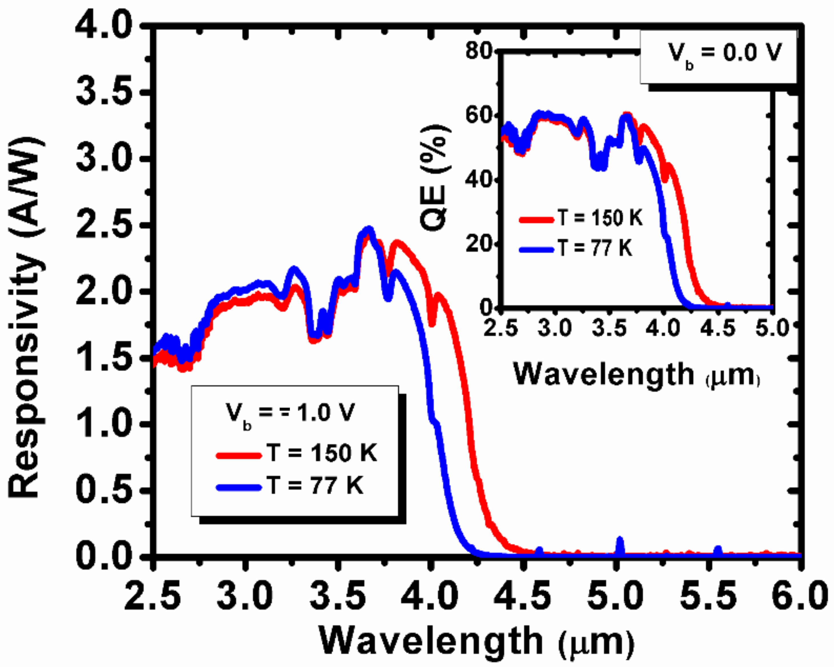
In order to verify the cut-off wavelength of the MWIR superlattice and draw a baseline for the performance of the device in the low-voltage regime, the optical performance of the devices is shown in Figure 1. In general, the responsivity of a detector is the ratio of the output electrical power over the input optical signal. The responsivity can determine the optical efficiency in a macroscopic scale of power. At 150 and 77 K, the device responsivity reaches a peak value of 2.49 and 2.32 A/W at 3.75 µm under −1.0 V applied bias, respectively (Figure 1). The device exhibits a 100% cut-off wavelength of 4.6 µm at 150 K and 4.30 µm at 77 K. At zero bias voltage, the peak of quantum efficiency (QE) of the APD was measured to be 58% at 77 K and 54 % at 150 K for the wavelength of 3.63 µm. The inset of the Figure 1, demonstrates the QE spectrum of the MWIR APD device at different wavelengths at the zero bias voltage. This can determine the efficient performance of the superlattice detector device at zero bias voltage across the MWIR region. Almost uniform values for the quantum efficiency across the whole spectrum from 2.5 µm toward the MWIR region implies the high quality of superlattice material.
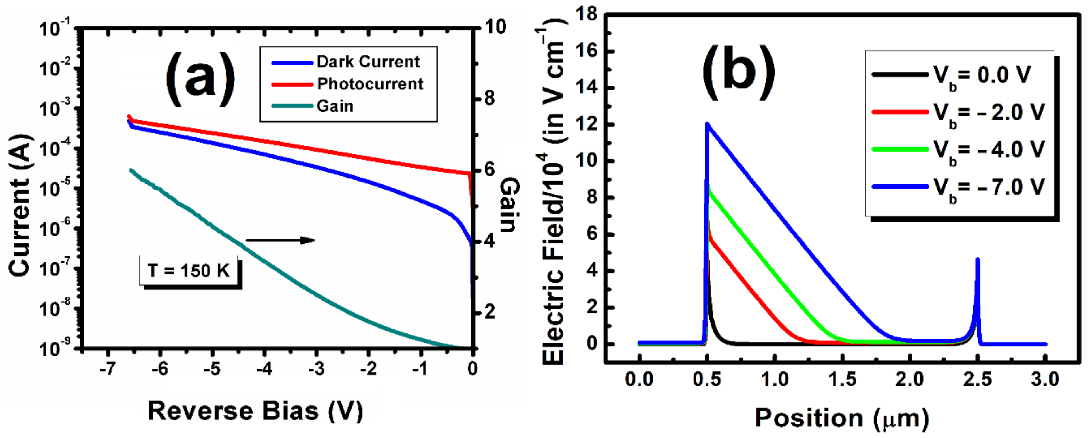
Current-voltage (I-V) measurements were carried out using Agilent 4156 c semiconductor parameter analyzer. The temperature of the devices was varied from 77 to 150 K to study the change in gain characteristics at different temperatures. A 633 nm He-Ne laser with an incident power of 5.0 mW was used to measure the photocurrent and the gain of the APDs. The calculation of the multiplication gain was performed by normalizing the photocurrent, i.e., the difference between light and dark currents, by the difference between the primary un-multiplied current and the un-multiplied dark current. Figure 2a shows the typical breakdown I-V characteristics and gain characteristics of a 100 × 100 µm2 MWIR APD with a maximum multiplication gain of around 6.0 at a reverse bias voltage of −6.5 V at 150 K. The devices show a soft avalanche breakdown starting at ~−3.0 V. The gain then increases until saturating at a gain of ~ 6 at a reverse bias of −6.5 V. The unity optical gain occurs at −1.3 V applied bias with a dark current of 1.83 × 10⁻⁵ A, where the photocurrent at the same voltage was measured to be 3.65 × 10⁻⁴ A. In order to give a better prospect of the distribution of electric field intensity in the APD device, we investigated the electric field build-up in the multiplication region using a 1D finite element model [24]. Plots of the evolution of the simulated electric field profile are shown below in Figure 2b. From this model, it is possible to estimate the peak of the electric field at the unity gain to be ~ 40 KV·cm−1, which increases to the peak of ~120 KV·cm−1 at −6.5 V where the maximum gain is reached. However, it is possible that the peak electric field may be larger due to the inhomogeneity of the doping and ionized defects. This model only considers the average electric field in the plane of the device. This model neglects the piezoelectric fields due the strained layers.
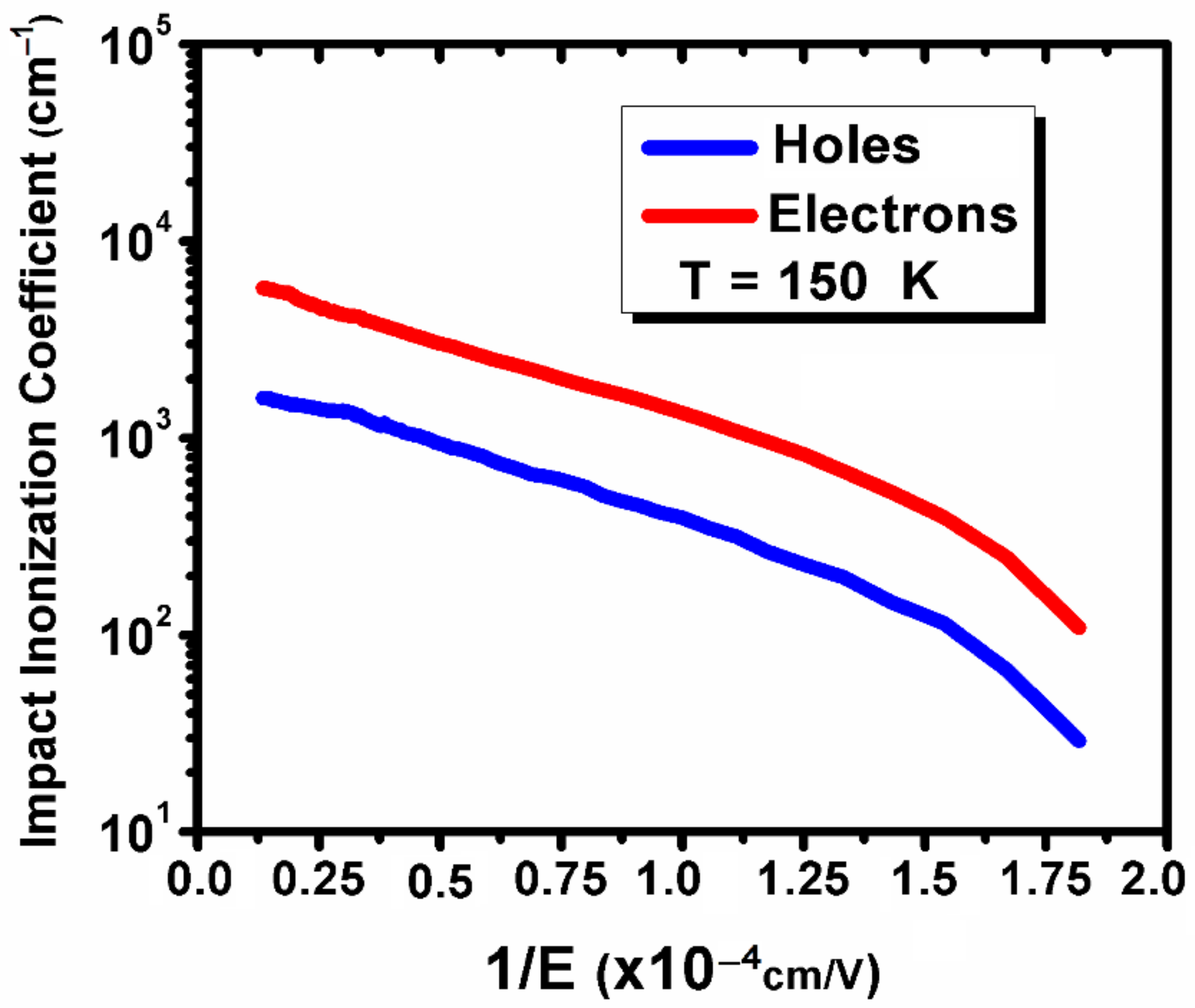
Figure 3 presents the hole and electron ionization coefficients for InAs/InSb MWIR APD as a function of the inverse electric field. The avalanche gain is primarily dependent upon two material parameters: the electron and hole impact ionization coefficients α and β. The gain can thus be split into electron and hole terms (Mn and Mp, respectively) and represented in terms of the ionization coefficients. The α and β are calculated using the multiplication gain under front and back illumination using the following equations [25]:
where Mn and Mp are the multiplication gain as a function of voltage and W stands for the depletion region width which is assumed to be the width of the absorber layer (i-InAs/InSb). Because of very low doping of the absorption/multiplication region, the electric field is nearly constant across this region. We illuminated the device from either top p+ contact and top n+ contact to control the dominate carrier injection into the multiplication region [25]. For the top contact illumination of n+ contact, the device with flipped structure was grown and processed under the same condition. The large difference in α and β (see Figure 3) under these different injection regimes is direct evidence that the effective α is greater than β. It also implies that the avalanche multiplication process is dominated by the impact ionization of electrons. The overall trend of the gain depicted in Figure 2, along with the large difference in electron and hole impact ionization coefficients of the gain, indicates a single-carrier-dominated avalanche mechanism, as seen in similar MWIR APDs [26,27]. The impact ionization coefficient (β/α = k) for the MWIR APD was calculated to be 0.27, which, for the p-i-n III-V structure, is acceptable, but it is still much greater than the reported cases for HgCdTe APDs. As demonstrated by McIntyre [28], a large difference in the ionization rates for electrons and holes is essential for a low noise avalanche photodiode. The multiplication process introduces excess noise due to statistical fluctuations in the number of secondary carriers created per avalanche event. Therefore, enhancing the k value for InAs/InSb MWIR APD can be considered for the future direction of this study, using a separate absorption multiplication design or bandstructure-engineered avalanche regions [29,30].
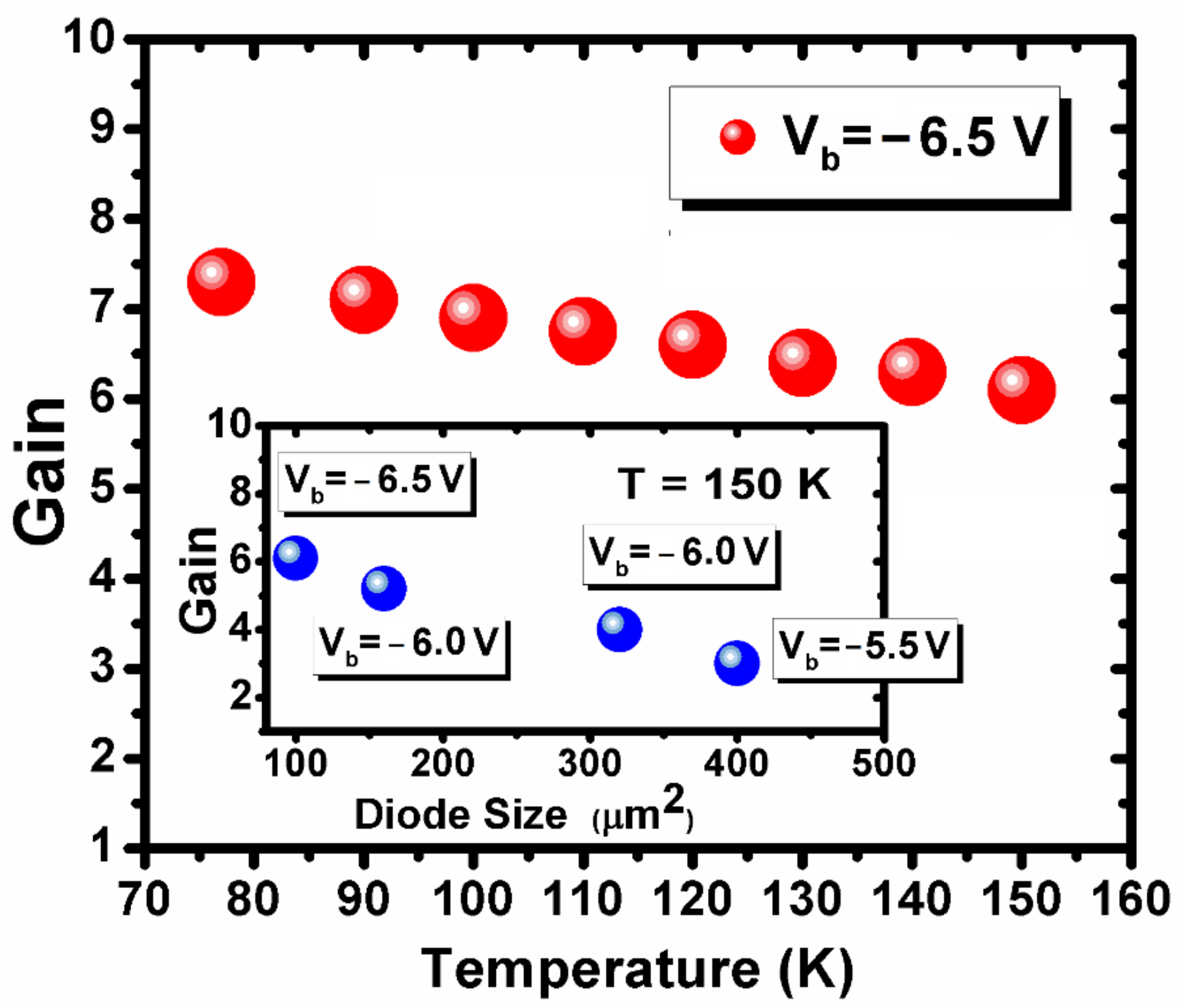
The gain of the device was measured at different temperature as illustrated in Figure 4. At 77 K, the gain of device reached to 7.4 at −6.5 V bias voltage. This value is close to the previous reports for III-V based APDs at 77K [11,12]. The temperature-dependent gain characteristic shows a continuous decrease in the multiplication gain at higher temperatures. The decrease of the gain at higher temperatures is due to a higher probability of carrier-carrier scattering and a higher loss of kinetic energy of carriers via various scattering mechanisms.
The inset of Figure 4 demonstrates the gain value for APDs with different diode sizes at 150 K by testing several devices. The corresponding voltage that each gain was measured is shown next to each gain value. The highest gain of 6 was obtained for the smallest APD size (100 µm). All the devices with different areas showed gain but the gain value was decreased slowly by increasing the size of the diodes, which could be related to higher dark current for larger sizes.
3. Materials and Methods
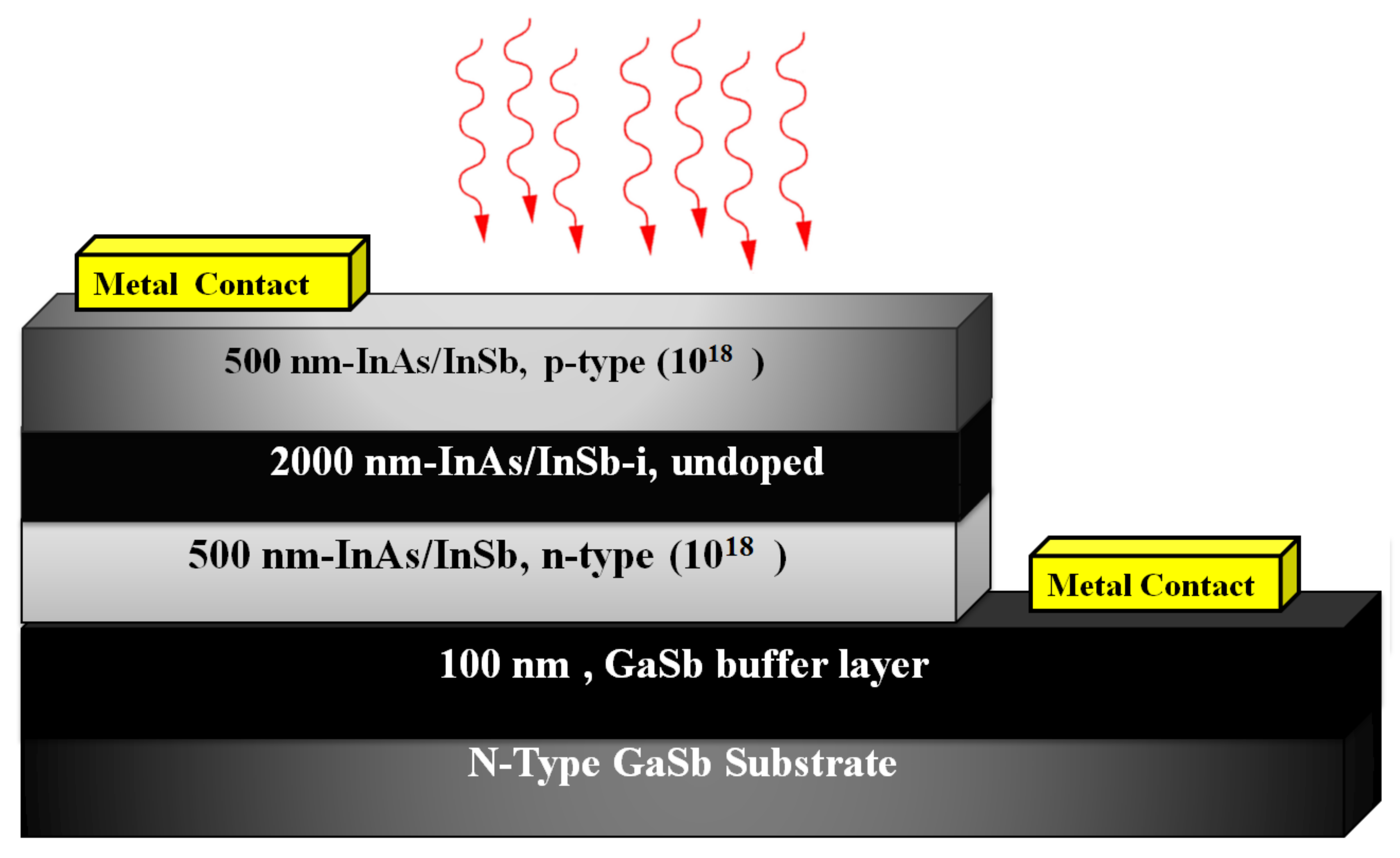
The APD MWIR photodetector was grown on 2-inch Te-doped n-type (1017 cm−3) GaSb (100) substrate using an Intevac Modular Gen II molecular beam epitaxy (MBE) system (Veeco Corporate, Plainview, NY, USA) equipped with As and Sb valved cracker sources. After deoxidizing the surface, in order to smooth out the surface of the substrate, a 200-nm-thick GaSb buffer layer was grown as the first step. Then, the whole p-i-n structure of InAs/InSb superlattice (11 ML of InAs and 2 ML of InSb) was grown as it is shown in Figure 5. The structure has 0.5 µm bottom n-contact (10 × 18 cm−3), 2.0 µm unintentionally doped absorption i-region, and 0.5 µm top p-contact (10 × 18 cm−3). Silicon and beryllium were used for n-type and p-type dopant, respectively. The doping concentrations of different regions were optimized and monitored using strict temperature control during growth and capacitance-voltage measurement. The structural properties of the superlattices were evaluated after growth using high resolution X-ray diffraction (HRXRD) and atomic force microscopy (AFM). The material was then fabricated into circular photodetectors with mesa diameters ranging from 100 to 400 μm. Mesa-isolated etching was performed by a combined inductively coupled plasma (ICP, Oxford Instruments) dry etching and citric-acid-based wet etching technique. Both the top and bottom contacts were formed using electron-beam-deposited Ti/Au. The devices were passivated for protection and insulation purposes by 600 nm SiO2 using plasma-enhanced chemical vapor deposition (PECVD, Oxford Instruments). The detail about the fabrication can be found somewhere else [31]. The passivation was aimed to minimize the contribution of surface leakage to the dark current [32]. Photodiodes were mounted onto a 68-pin leadless chip carrier (LCC) with indium for electrical and optical characterization. The connections from the top and bottom contacts of the sample to the bond pads of the LCC were made with a resistance-heated thermo compression wire bonder.
After fabrication, the devices were characterized using a temperature- and pressure-controlled Janis STVP-100 two-chamber liquid helium cryostat station (Janis Research, Woburn, MA, USA) with 300 K background. The optical response of the InAs/InSb superlattice MWIR APD was done at 150 K under front-side illumination. No anti-reflection coating was applied to the devices. The optical response result was divided into relative spectral response and blackbody integrated response sub-measurements. The photodetector spectral response was measured using a Bruker IFS 66 v/S Fourier transform infrared spectrometer (FTIR) and the absolute responsivity of the device was calculated using a band-pass filter in front of the calibrated blackbody source at 1000 °C.
4. Conclusions
In summary, Antimony-based III/V material structure was implemented to demonstrate MWIR APD devices. The structure is a homojunction structure grown on GaSb substrate grown by MBE. The device exhibits a 100 % cut-off wavelength of 4.6 µm at 150 K. At 150, the QE of 54% was measured at zero applied bias voltage. The electron and hole impact ionization coefficients for the MWIR APD device were calculated and compared with each other to give a better prospect of the performance. This leads to extracting the impact ionization coefficient with the value of 0.27 for the MWIR APD, which needs to be improved using different architecture for the device structure, by implementing the concept of heterostructures along with a separate absorption multiplication design.
Author Contributions
A.D. performed the photodetector design, fabrication and electro-optical characterization and wrote the paper. J.L. performed MBE growth and characterization of material, L.G. performed structural characterization and M.R. provided the idea and supervised the project. All authors have read and agreed to the published version of the manuscript.
Funding
This research received no external funding.
Acknowledgments
Authors would like to acknowledge the support, interest, and encouragement of Whitney Mason from DARPA, Michael Gerhold and Tania Paskova from the U.S. Army Futures Command, Kurt Eyink from the U.S. Air Force Research Laboratory, Murzy Jhabvala from NASA Goddard Space Flight Center, Meimei Tidrow from the U.S. Army Night Vision, Laboratory, Gail Brown from CQD/NU.
Conflicts of Interest
The authors declare no conflict of interest. The funders had no role in the design of the study; in the collection, analyses, or interpretation of data; in the writing of the manuscript, or in the decision to publish the results.
References
- Campbell, J.C. Recent Advances in Telecommunications Avalanche Photodiodes. J. Lightwave Technol. 2007, 25, 109–121. [Google Scholar] [CrossRef] [Green Version]
- Razeghi, M. Fundamentals of Solid State Engineering; Springer: Berlin/Heidelberg, Germany, 2006. [Google Scholar]
- James, W.B.; Richard, B.; David, G.; Donald, L.; Markus, L.; Eric, C.P.; Thomas, S.; William, E.T.; Majid, Z.; Joseph, Z. Teledyne Imaging Sensors: Infrared imaging technologies for astronomy and civil space. SPIE Astron. Telesc. Instrum. 2008, 7021, 70210. [Google Scholar]
- Gehrz, R.D.; Becklin, E.E.; de Pater, I.; Lester, D.F.; Roellig, T.L.; Woodward, C.E. A new window on the cosmos: The Stratospheric Observatory for Infrared Astronomy (SOFIA). Adv. Space Res. 2009, 44, 413–432. [Google Scholar] [CrossRef]
- Ring, E.F.J.; Ammer, K. Infrared thermal imaging in medicine. Physiol. Meas. 2012, 33, R33–R46. [Google Scholar] [CrossRef] [PubMed]
- Wu, D.; Li, J.; Dehzangi, A.; Razeghi, M. Mid-wavelength infrared high operating temperature pBn photodetectors based on type-II InAs/InAsSb superlattice. AIP Adv. 2020, 10, 025018. [Google Scholar] [CrossRef] [Green Version]
- Dehzangi, A.; Wu, D.; McClintock, R.; Li, J.; Razeghi, M. Planar nBn type-II superlattice mid-wavelength infrared photodetectors using zinc ion-implantation. Appl. Phys. Lett. 2020, 116, 221103. [Google Scholar] [CrossRef]
- Kerlain, A.; Bonnouvrier, G.; Rubaldo, L.; Decaens, G.; Reibel, Y.; Abraham, P.; Rothman, J.; Mollard, L.; de Borniol, E. Performance of Mid-Wave Infrared HgCdTe e-Avalanche Photodiodes. J. Electron. Mater. 2012, 41, 2943–2948. [Google Scholar] [CrossRef]
- Rogalski, A. HgCdTe infrared detector material: History, status and outlook. Rep. Prog. Phys. 2005, 68, 2267. [Google Scholar] [CrossRef] [Green Version]
- Perrais, G.; Rothman, J.; Destefanis, G.; Chamonal, J.-P. Impulse Response Time Measurements in Hg0.7Cd0.3Te MWIR Avalanche Photodiodes. J. Electron. Mater. 2008, 37, 1261–1273. [Google Scholar] [CrossRef]
- Maddox, S.J.; Sun, W.; Lu, Z.; Nair, H.P.; Campbell, J.C.; Bank, S.R. Enhanced low-noise gain from InAs avalanche photodiodes with reduced dark current and background doping. Appl. Phys. Lett. 2012, 101, 151124. [Google Scholar] [CrossRef] [Green Version]
- Abautret, J.; Perez, J.P.; Evirgen, A.; Rothman, J.; Cordat, A.; Christol, P. Characterization of midwave infrared InSb avalanche photodiode. J. Appl. Phys. 2015, 117, 244502. [Google Scholar] [CrossRef]
- Sai-Halasz, G.A.; Tsu, R.; Esaki, L. A new semiconductor superlattice. Appl. Phys. Lett. 1977, 30, 651–653. [Google Scholar] [CrossRef]
- Wei, Y.; Razeghi, M. Modeling of type-II InAs/GaSb superlattices using an empirical tight-binding method and interface engineering. Phys. Rev. B 2004, 69, 085316. [Google Scholar] [CrossRef]
- Razeghi, M.; Dehzangi, A.; Wu, D.; McClintock, R.; Zhang, Y.; Durlin, Q.; Li, J.; Meng, F. Antimonite-based gap-engineered type-II superlattice materials grown by MBE and MOCVD for the third generation of infrared imagers. 2019. In Infrared Technology and Applications XLV; International Society for Optics and Photonic: Bellingham, WA, USA, 2019; Volume 11002, p. 110020G. [Google Scholar]
- Hoang, A.M.; Dehzangi, A.; Adhikary, S.; Razeghi, M. High performance bias-selectable three-color Short-wave/Mid-wave/Long-wave Infrared Photodetectors based on Type-II InAs/GaSb/AlSb superlattices. Sci. Rep. 2016, 6, 24144. [Google Scholar] [CrossRef] [PubMed] [Green Version]
- Razeghi, M.; Haddadi, A.; Dehzangi, A.; Chevallier, R.; Yang, T. Recent advances in InAs/InAs1-xSbx/AlAs1-xSbx gap-engineered type-II superlattice-based photodetectors. Infrared Technol. Appl. XLIII 2017, 10177, 1017705. [Google Scholar]
- Razeghi, M.; Haddadi, A.; Hoang, A.M.; Chevallier, R.; Adhikary, S.; Dehzangi, A. InAs/InAs1-xSbx type-II superlattices for high performance long wavelength infrared detection. Appl. Phys. Lett. 2014, 105, 121104. [Google Scholar]
- Dehzangi, A.; McClintock, R.; Haddadi, A.; Wu, D.; Chevallier, R.; Razeghi, M. Type-II superlattices base visible/extended short–wavelength infrared photodetectors with a bandstructure-engineered photo–generated carrier extractor. Sci. Rep. 2019, 9, 5003. [Google Scholar] [CrossRef] [Green Version]
- Dehzangi, A.; McClintock, R.; Wu, D.; Haddadi, A.; Chevallier, R.; Razeghi, M. Extended short wavelength infrared heterojunction phototransistors based on type II superlattices. Appl. Phys. Lett. 2019, 114, 191109. [Google Scholar] [CrossRef]
- Haddadi, A.; Adhikary, S.; Dehzangi, A.; Razeghi, M. Mid-wavelength infrared heterojunction phototransistors based on type-II InAs/AlSb/GaSb superlattices. Appl. Phys. Lett. 2016, 109, 021107. [Google Scholar] [CrossRef]
- Dehzangi, A.; Haddadi, A.; Adhikary, S.; Razeghi, M. Impact of scaling base thickness on the performance of heterojunction phototransistors. Nanotechnology 2017, 28, 10LT01. [Google Scholar] [CrossRef]
- Li, J.; Dehzangi, A.; Wu, D.; McClintock, R.; Razeghi, M. Type-II superlattice-based heterojunction phototransistors for high speed applications. Infrared Phys. Technol. 2020, 108, 103350. [Google Scholar] [CrossRef]
- Winston, D.; Hayes, R. SimWindows—A New Simulator for Studying Quantum-Well Optoelectronic Devices. Compd. Semicond. 1995, 141, 747–750. [Google Scholar]
- Oguzman, I.H.; Bellotti, E.; Brennan, K.F.; Kolnik, J.; Wang, R.P.; Ruden, P.P. Theory of hole initiated impact ionization in bulk zincblende and wurtzite GaN. J. Appl. Phys. 1997, 81, 7827–7834. [Google Scholar] [CrossRef]
- Mallick, S.; Banerjee, K.; Ghosh, S.; Plis, E.; Rodriguez, J.B.; Krishna, S.; Grein, C. Ultralow noise midwave infrared InAs-GaSb strain layer superlattice avalanche photodiode. Appl. Phys. Lett. 2007, 91, 241111. [Google Scholar] [CrossRef]
- Kinch, M.; Beck, J.; Wan, C.-F.; Ma, F.; Campbell, J. HgCdTe electron avalanche photodiodes. J. Electron. Mater. 2004, 33, 630–639. [Google Scholar] [CrossRef]
- McIntyre, R.J. Multiplication noise in uniform avalanche diodes. IEEE Trans. Electron Devices 1966, ED-13, 164–168. [Google Scholar] [CrossRef]
- Capasso, F.; Won-Tien, T.; Williams, G.F. Staircase solid-state photomultipliers and avalanche photodiodes with enhanced ionization rates ratio. IEEE Trans. Electron Devices 1983, 30, 381–390. [Google Scholar] [CrossRef]
- Ren, M.; Maddox, S.J.; Woodson, M.E.; Chen, Y.; Bank, S.R.; Campbell, J.C. AlInAsSb separate absorption, charge, and multiplication avalanche photodiodes. Appl. Phys. Lett. 2016, 108, 191108. [Google Scholar] [CrossRef]
- Haddadi, A.; Dehzangi, A.; Chevallier, R.; Adhikary, S.; Razeghi, M. Bias-selectable nBn dual—band long—/very long—wavelength infrared photodetectors based on InAs/InAs1-xSbx/AlAs1-xSbx type-II superlattices. Sci. Rep. 2017, 7, 3379. [Google Scholar] [CrossRef] [Green Version]
- Dehzangi, A.; Durlin, Q.; Wu, D.; McClintock, R.; Razeghi, M. Investigation of surface leakage reduction for small pitch shortwave infrared photodetectors. Semicond. Sci. Technol. 2019, 34, 06LT01. [Google Scholar] [CrossRef]
Sample Availability: Samples of the compounds are not available from the authors. |
Figure 1.
Responsivity spectra measured under front-illumination at 150 and 77 K under −1.0 V bias voltage. (Inset) Quantum efficiency spectrum of the MWIR APD at zero bias voltage.
Figure 1.
Responsivity spectra measured under front-illumination at 150 and 77 K under −1.0 V bias voltage. (Inset) Quantum efficiency spectrum of the MWIR APD at zero bias voltage.

Figure 2.
(a) Breakdown characteristics and gain of the MWIR APD device. Dark current and photocurrent are shown on the left axis; gain is shown on the right axis. (b) Simulation of electric field profile under various applied reverse biases of the MWIR APD device.
Figure 2.
(a) Breakdown characteristics and gain of the MWIR APD device. Dark current and photocurrent are shown on the left axis; gain is shown on the right axis. (b) Simulation of electric field profile under various applied reverse biases of the MWIR APD device.

Figure 3.
Hole and electron ionization coefficients for MWIR APD vs. inverse of electric field.

Figure 4.
Temperature-dependent gain characteristics of the APD. Inset: Gain as a function of device area at 150 K. The corresponding voltage at which each gain was measured is shown next to each gain value.
Figure 4.
Temperature-dependent gain characteristics of the APD. Inset: Gain as a function of device area at 150 K. The corresponding voltage at which each gain was measured is shown next to each gain value.

Figure 5.
Schematic of the mid-wavelength infrared (MWIR) avalanche photodiode (APD) structure under top illumination.
Figure 5.
Schematic of the mid-wavelength infrared (MWIR) avalanche photodiode (APD) structure under top illumination.

Publisher’s Note: MDPI stays neutral with regard to jurisdictional claims in published maps and institutional affiliations. |
© 2020 by the authors. Licensee MDPI, Basel, Switzerland. This article is an open access article distributed under the terms and conditions of the Creative Commons Attribution (CC BY) license (http://creativecommons.org/licenses/by/4.0/).
Share and Cite
MDPI and ACS Style
Dehzangi, A.; Li, J.; Gautam, L.; Razeghi, M. Avalanche Photodetector Based on InAs/InSb Superlattice. Quantum Rep. 2020, 2, 591-599. https://0-doi-org.brum.beds.ac.uk/10.3390/quantum2040041
AMA Style
Dehzangi A, Li J, Gautam L, Razeghi M. Avalanche Photodetector Based on InAs/InSb Superlattice. Quantum Reports. 2020; 2(4):591-599. https://0-doi-org.brum.beds.ac.uk/10.3390/quantum2040041
Chicago/Turabian StyleDehzangi, Arash, Jiakai Li, Lakshay Gautam, and Manijeh Razeghi. 2020. "Avalanche Photodetector Based on InAs/InSb Superlattice" Quantum Reports 2, no. 4: 591-599. https://0-doi-org.brum.beds.ac.uk/10.3390/quantum2040041