Review

Optical Fibre Micro/Nano Tips as Fluorescence-Based Sensors and Interrogation Probes

1
Institute of Applied Physics “Nello Carrara”, IFAC-CNR; via Madonna del Piano 10, 50019 Sesto Fiorentino (FI), Italy
2
National Institute of Optics, INO-CNR, Largo Fermi 6, 50125 Firenze, Italy
3
Institute for Complex Sistems, ISC-CNR, Via Madonna del Piano 10, 50019 Sesto Fiorentino (FI), Italy
*
Author to whom correspondence should be addressed.
Submission received: 24 July 2020 / Revised: 21 August 2020 / Accepted: 24 August 2020 / Published: 27 August 2020
(This article belongs to the Special Issue Recent Development of Resonance-Based Optical Sensors and Biosensors)

Abstract

:
Optical fibre micro/nano tips (OFTs), defined here as tapered fibres with a waist diameter ranging from a few microns to tens of nanometres and different tip angles (i.e., from tens of degrees to fractions of degrees), represent extremely versatile tools that have attracted growing interest during these last decades in many areas of photonics. The field of applications can range from physical and chemical/biochemical sensing—also at the intracellular levels—to the development of near-field probes for microscope imaging (i.e., scanning near-field optical microscopy (SNOM)) and optical interrogation systems, up to optical devices for trapping and manipulating microparticles (i.e., optical tweezers). All these applications rely on the ability to fabricate OFTs, tailoring some of their features according to the requirements determined by the specific application. In this review, starting from a short overview of the main fabrication methods used for the realisation of these optical micro/nano structures, the focus will be concentrated on some of their intriguing applications such as the development of label-based chemical/biochemical sensors and the implementation of SNOM probes for interrogating optical devices, including whispering gallery mode microcavities.

1. Introduction

Thanks to their capability of guiding light with low losses, intrinsic flexibility, and immunity to any electromagnetic interferences, optical fibres represent a key element in many technological fields, from optical communications to the development of robust, reliable, and high-performance diagnostic systems and optical sensors [1,2,3,4,5,6]. Furthermore, the possibility of reducing their radial dimension to values lower than the light propagation wavelength has widened the horizon of their possible applications towards new and intriguing investigative scenarios, until now unthinkable to be achieved with standard unmodified optical fibres [7,8]. In many cases, it is the far end of the fibre that is interested in size/shape modifications. In particular, when it assumes a conical shape, it is normally named the “tip”. Different from what is reported in the extensive review work carried out by J.S. Paiva and co-workers on this topic [9], where the term “tip” is synonymous with the “end of the fibre” regardless of its geometry and dimension, here, we define the optical fibre micro/nano tip as a tapered fibre with a waist diameter ranging from few microns to tens of nanometres and different tip angles (i.e., from tens of degree to fractions of a degree).
This optical tool represents a remarkable example of how a single device can pave the way for a large number of applications in photonics. The reason for this fact has to be found in its ability to control and confine light radiation, which propagates inside the fibre, up to nanometric scale. The spatial subwavelength confinement contributes to increasing the electromagnetic field intensity in its surrounding region. This phenomenon allows it to behave like optical tweezers capable of trapping and manipulating nanoparticles through a remote field action [10,11,12].
On the other hand, as the light beam inside the fibre approaches the very end of the tip, the evanescent field component becomes broader and broader, extending towards the surrounding medium. In order to prevent the unavoidable field leakage through the side walls of the tip while maintaining a high sensitivity at its apex, a metallic or high-index dielectric thin film coating is generally used with the aim of probing either any change of physical parameters (i.e., temperature, force, refractive index) [13,14,15] or the mere presence of chemical/biochemical species in small volumes [16,17,18,19,20,21,22,23,24]. Moreover, its nanometric size allows to carry out minimally invasive analyses and/or to trigger specific actions in extremely small environments such as cells for sensing and theranostics [25,26,27,28,29,30,31,32,33,34,35,36,37,38]. This feature has led to their extensive use in surface plasmon resonance (SPR) or localised surface plasmon resonance (LSPR) [39,40,41,42], surface enhanced Raman scattering (SERS) [43,44,45,46,47], and tip enhanced Raman scattering (TERS) applications [48,49,50].
Finally, optical fibre micro/nano tips (OFTs) find a direct application in many non-invasive techniques for optical characterisation of substrates and devices such as the scanning near-field optical microscopy (SNOM) [51,52,53,54,55,56,57,58,59] and atomic force microscopy (AFM)-based SNOM (AFM/SNOM) [60,61,62,63,64,65]. Unlike standard microscopy techniques, which are generally limited in resolution to half of the excitation wavelength owing to the diffraction phenomenon as expressed by the Abbe condition [66,67], these techniques are, in principle, not limited by diffraction or, more precisely, their only limit is represented by the radial size of the realised nanotip [68]. This unique feature allows these investigation methods to take a look at how light propagates within micro/nanophotonic devices, such as channel waveguides [69,70,71,72], optical fibres [73], photonic crystal structures [74,75,76], and whispering gallery mode (WGM) microcavities [77,78,79,80,81]. The acquisition of this information by these techniques makes it possible to optimise the design and the fabrication of the same devices, leading to more and more efficient performances.
All these uses rely on the ability to fabricate this kind of micro/nano tip, tailoring some of their features according to the particular application [9]. In this review, starting from a short overview on the fabrication methods generally used for the realisation of these optical micro/nano structures, our attention will be focused on some of their intriguing applications so far not fully covered in other reviews, such as the development of fluorescence-based chemical/biochemical sensors and the implementation of SNOM probes for interrogating optical materials and devices including whispering gallery mode microcavities.

2. Fabrication Techniques

Optical micro/nano tips can be fabricated using different techniques that have been developed over a long period of time and adapted according to specific application requirements or technological standards of that time. Looking for the best fabrication technique to obtain the right device for the application under study, different aspects should be taken into account, including reproducibility, time, simplicity, required instrumentation, cost, possibility of batch processing, and so on, arriving at a trade-off between geometrical precision, optical performance, and cost [9]. In a plethora of continuously emerging techniques, it is not so obvious to classify fabrication methods, despite that some of them, such as chemical etching, thermal pulling, and grinding and polishing, are generally considered as low cost, while femtosecond laser milling or focused ion beam milling (FIB) can be considered as expensive or complex. Technology evolution can change this classification, for example, providing some advantages to a particular method, which were unavailable before. Moreover, the techniques can be combined, improving the result compared with the original methods. Some details about these techniques are briefly reported here, while a deeper description can be found in [9].

2.1. Grinding and Polishing

In this mechanical process, the tip shape is obtained by combining the rotation of the fibre along its principal axis with the rotation of an abrasive disc, with the cone angle of the final tip determined by a function of the angle between these two axes of rotation. The contact of the fibre with the abrasive surface is usually ensured by a high-precision translational stage. This method is simple and low-cost. Some concerns can be related to mechanical vibrations, off-axes rotations, and other mechanical issues that can impact the quality and shape of the final tip [9].

2.2. Thermal Pulling

This process consists of a local heating (usually performed using a flame, a CO2 laser or an electric discharge) of a stripped fibre, which softens the optical fibre and allows to pull it apart. Two tips are then shaped, usually showing a flat plateau at the apex and a lower surface roughness with respect to the results achieved with other methods. Although thermal pulling is a low-cost method, its intrinsic nature leads to a high sensitivity to environmental factors, while the tip shape depends on many fabrication parameters, such as the pulling speed [82].

2.3. Chemical Etching Methods

The static etching method, also named Turner’s method [83], relies on the idea that a fibre has to be simply dipped into a hydrofluoric acid solution. In the original Turner’s method, a protective liquid layer (e.g., organic solvent) is added to control the height of the acid meniscus formed at the interface with the dipped fibre. Moreover, the overlayer has the practical utility to block the evaporation of acid vapours, preventing the inevitable corrosion of the fibre above the interface. The principal drawbacks are that the surface roughness cannot be controlled and the process is not self-limiting. The tube etching method [84] was designed to prevent or reduce these drawbacks, using the same idea of Turner, but without stripping the plastic coating of the fibre (resistant to acid attack). Both methods are strongly dependent on fabrication parameters such as etching solution concentration and etching time, and on external factors such as environmental temperature and mechanical vibrations, which affect the physical properties and the stability of the meniscus at the interface between the fibre and acid solution. Modifications and evolutions of these ideas can be found in [55,85,86,87,88,89,90,91,92].

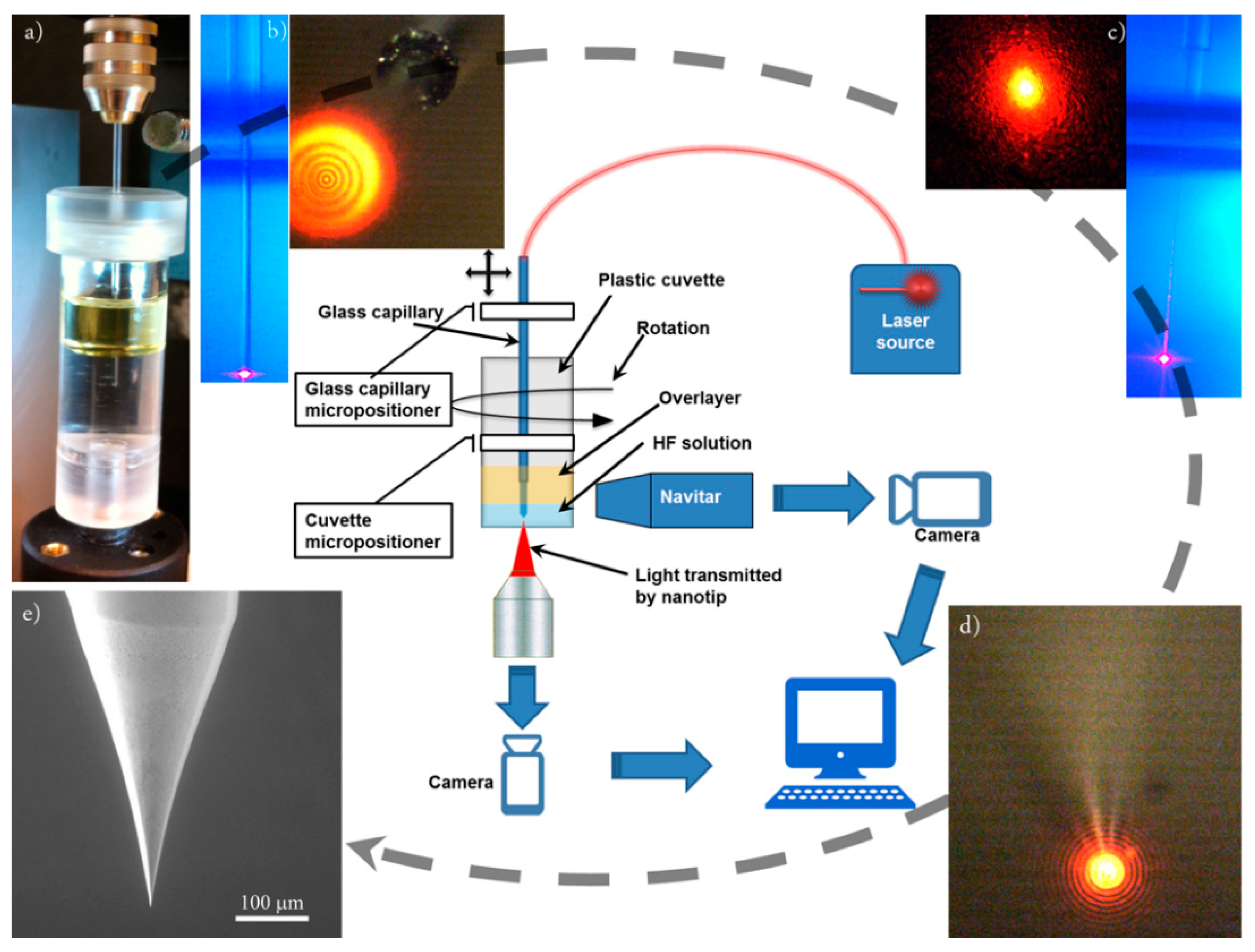
A Mixed Mechanical-Chemical Etching Method

As a modification of the Turner’s chemical etching method, the Wing method (WM) has been widely reported [24,93,94]. The term wing refers to the profile of the nanotip obtained in set-up conditions with high velocity, in comparison with the two other methods mentioned in the previous paragraph (static etching and tube etching). In the WM set-up (Figure 1), the stripped (jacket removed) optical fibre end is dipped into a vial containing an aqueous hydrogen fluoride (HF) solution (usually between 1% and 50%) covered with a protection layer (e.g., organic oil in many cases). The vial and the optical fibre are connected to different motors, allowing them to rotate independently around the fibre and the vial axis, respectively. The vial and the optical fibre are equipped with precision translation stages, for alignment of the fibre on the rotation axis of the vial. After an appropriate setting of the set-up parameters (rotation velocities of optical fibre and vial, HF concentration in the solution, organic overlayer), the fabrication is ready to start. Although the WM mainly refers to chemical etching combined with mechanical rotation, in general, it is possible to use another mechanical movement, such as the extraction of the fibre from the HF solution during the etching, that can modify the geometrical shape of the nanotip. This added degree of freedom can be used in many situations, affecting in particular the angle at the apex of the nanotip.
Trying to overcome the drawbacks of the original Turner’s method, the authors of the present review realised that the friction force between the optical fibre and the etching liquid could be used to shape the nanotip [93]. This friction force can be made and, within a certain limit, controlled using the coupling between the rotation of the fibre and the rotation of the vial. In this way, different fluid-dynamical regimes on the liquids inside the vial solution (HF solution plus overlayer) can be obtained, which modify the force field acting on the fibre and then the etching conditions. Thanks to all these tricks, tip parameters can be modified by changing the ratio between the angular velocities, the ratio between optical fibre and vial axis radius, and the extraction velocity. It is worth noting that this method allows to monitor the etching process, when coupling the optical fibre with laser light.

2.4. Micromachining Methods

This category includes high resolution methods, usually complex and expensive, but capable of allowing the design of complex patterned structures in different kinds of substrates with high accuracy and reproducibility.

2.4.1. Focused Ion Beam (FIB) Milling

FIB milling is able to fabricate several optical fibre tips and tailored structures created on top of the fibre such as miniaturised tweezers and microcantilevers. FIB reaches nanometre-scale resolutions, de facto being one of the most suitable methods for patterning, cross-sectioning, and/or functionalizing a subwavelength microfibre, opening new possibilities for ultra-small size fibre-based devices [11,95,96,97,98,99,100,101,102].

2.4.2. Femtosecond Laser Machining

This micromachining technique is based on material ablation owing to absorbed energy above a threshold, and it has been used to build structures on the top of a cleaved fibre [9] thanks to its high spatial resolution [103,104,105].

2.4.3. Lithography

Lithographic fabrication refers to micromoulding methods where the topography of a template defines the micro/nano patterns created on the top of an optical fibre (or, in general, onto a substrate). The process is based on the use of mechanical pressure, photons, or electrons, giving rise, for optical fibre tips, to general categories as interference lithography, electro-beam lithography, and nanoimprint lithography [9].

2.5. Other Methods

Photopolymerisation Methods

Microstructures based on polymeric chains can be fabricated on the top of optical fibres by free radical guided photopolymerisation (e.g., optical fibre tweezers, micro lenses, optical fibre sensors) [11,63,106,107,108,109,110,111,112,113,114]. In this fabrication technique, essentially, a photo sensitive liquid is deposited on the top of a cleaved fibre, followed by irradiation through the fibre core. This procedure, thanks to a self-guiding effect, leads to the manufacturing of specific structures at the fibre end.
Table 1 summarizes the advantages and disadvantages of the different methods, in order to better compare the performances of the reported fabrication techniques used for fibre tip construction.

2.6. Physical and Optical Properties of the Fibre Tips

Fabrication techniques allow to build different kinds of micro/nano fibre tips, shaping their geometry and consequently their optical features. Depending on the specific application, some particular features can be required, such as a short tip or a large cone angle, a smooth roughness, and a high throughput from the distal end. However, it is worth remembering how all these geometrical features (tip angle, tip length, axial symmetry, and surface roughness) contribute in an interconnected and complex way to shape the optical properties of the fibre tip [115].

2.7. Coating Processes

The addition of an opaque metallic coating covering the walls of the fibre tip, leaving a tiny aperture at the end of the fibre, is the fundamental process in order to allow the propagation of light within the fibre tip. In fact, as the diameter of the tip decreases to micro or nanometric dimensions, efficient guiding of light is no longer assured and, even though, in principle, a fundamental mode still exists, the guided field extends well beyond the physical size of the tip, thus both propagation losses and interferences from the environment can become relevant. Metal deposition is, therefore, needed to reduce these effects and allow sufficient light to propagate through the tip up to the vertex [82]. Metal coating can be achieved using different methods such as vacuum deposition by means of evaporation or radio-frequency sputtering [39,116].
Different metals, such as aluminium, copper, gold, or metal oxides (titanium dioxide (TiO2)), can be used, always looking for a trade-off between opacity in the frequency range of interest, ease of processing, and cost. Regardless of the method chosen to coat the fibre tip, it is of paramount importance to take care of some aspects such as cleanliness of the fibre substrate before the coating, presence of metal grains on the surface after the coating, and a coating-less well-defined region near the tip to assure a good power throughput. Cleanliness is of utmost importance in tip fabrication, as atmospheric dust particles adhering to the fibre during the process create pinholes in the film by shadowing the source. Ultrasonic and chemical cleaning procedures can be used to prevent this problem. Any jacket residues must be removed, too. Organic decomposition products form the residue, preventing proper adhesion of the metal coating to the fibre surface and inducing pinhole formation. Large-grain films can contribute to serious problems in applications of fibre tips, with such films forming lossy metallic waveguides with a high incidence of small pinholes among the fibre walls. Grainy films can also induce the formation of jagged and pointed structures in the vicinity of the tip. The primary requisite for metallisation is, therefore, the deposition of smooth and continuous films having the smallest possible grain size. The use of ultraclean vacuum systems or the adoption clean-room conditions are highly recommended in the coating process. On the other hand, it should be considered that the roughness of the metal coating on the fibre tip surface opens the way to phenomena such as surface-enhanced Raman scattering (SERS) and tip-enhanced Raman scattering (TERS) [117].

3. Applications

3.1. Sensing Based on Optical Fibre Tips

Among all the possible OFT applications, their use as chemical and biochemical sensors has been considered very attractive in the past decades [9,39,118,119,120]. In this review, we will focus on fluorescent-based OFT sensors, providing only a few examples for those based on refractive index detection and surface-enhanced Raman spectroscopy (SERS), where a specific target is detected after its selective binding to a properly functionalised optical fibre nanotip, which generates a variation in the properties of the guided light, or based on chemiluminescence reactions.
An example of how to use OFT as a refractive index (RI) sensor was given by J.H. Tai et al. [121], who used a metal-free tip for this purpose. The sensing principle was based on the changes of the optical confinement at the nanotip. The increased environmental RI significantly enlarged the optical spot. The measurement setup was constituted by a 5 mW He–Ne laser coupled into the fibre, and by an objective (numerical aperture (NA) = 0.25) that collected the light emitted from the tip and then focused onto a silicon detector. A glass slide, on which a sample drop was deposited, was used to change the samples to be measured, that is, mixtures of pure water and glycerine at variable compositions. The authors emphasised the advantages of using a fibre tip such as the low sample volume required, the simplicity of the optical setup, and the possibility of performing real-time and high-speed monitoring of the RI changes. By changing both the NA of the objective used to collect the light emitted from the fibre tip and the quality of the tip (i.e., tip shape and size), different values for the OFT intensity sensitivity were demonstrated. For instance, in the RI working range from 1.33 to 1.43, the maximum value reached for the intensity sensitivity was ~8000%/RIU (Refractive Index Unit) achieved with an NA = 0.1, which implied the capability to detect 2.5 × 10⁻⁵ RIU at 0.2% stability of the laser intensity.
As demonstrated by Viets et al. in 2001 [43], the SERS intensity from an optical fibre-end can be enhanced by about a factor of 20 by optimising the inclination angle of the tip surface. Depending on the coating of the fibre, the optimal angle is comprised between 40° and 60° [122]. In another example of the OFT application to SERS, Scaffidi et al. [123] proposed a chemical sensor for pH detection in living cells, using para-mercaptobenzoic acid (pMBA) as a hydrogen-ion sensitive molecule. In particular, a silver island film deposition was realised onto the OFT, and the pH indicator, pMBA, was immobilised via a silver-thiol bond. The carboxyl group of pMBA is pH sensitive in the physiological range of interest. The SERS probe was inserted into the cells (HMEC-15/hTERT immortalised human mammary epithelial cells and PC-3 human prostate cancer cells) and SERS spectra were acquired. Interestingly, in addition to the properties of the SERS-active nanoprobe, it was demonstrated that its insertion into cells induces neither apoptosis nor an aggressive lysosomal response from the used cell lines.
Another example of not-fluorescence-based OFT sensors was given by Gao et al. [22], who presented in 1995, for the first time, a chemiluminescence-based sensor at the tip of an optical fibre. In particular, the authors determined the most efficient tip geometry for the detection of the light signal: the tip with the largest tapering angle was demonstrated to be the best configuration to collect light when the light source extends beyond the penetration depth of the evanescent wave, which is what happens during a chemiluminescence (CL) reaction. The suitable conditions were evaluated using a fluorophore (Rhodamine 6G) immobilised onto the tip of the fibre, using a thin layer of the dye in a sol–gel matrix. These results were applied to the chemiluminescence-based sensor developed for organophosphorus-based pesticide detection. The enzyme (alkaline phosphatase) was immobilised in the sol–gel layer onto the tapered tip and catalysed the substrate solution around the tip (the dephosphorylation of CSPD® substrate), which is responsible for the CL signal. The presence of the pesticides inhibits the enzyme–substrate reaction and determines a decrease of the CL signal. The CL signal was collected at the tip and transmitted to a CCD array detector; owing to the weakness of the signal, a bundle of four fibre-tips was used to increase its amplitude.
In the fluorescence-based OFT sensors, the sensing scheme generally involves four different cases: target not-fluorescent, then the detection molecule needs to be labelled with a fluorophore; target not-fluorescent, but the recognition element changes its fluorescence properties upon the interaction with the target; target not-fluorescent, but a fluorescent molecule is formed as product of an enzymatic catalysis; and the target itself is a fluorescent molecule. Detailed examples of fluorescence-based OFT sensor for chemical and biochemical targets are reported in the following paragraphs.

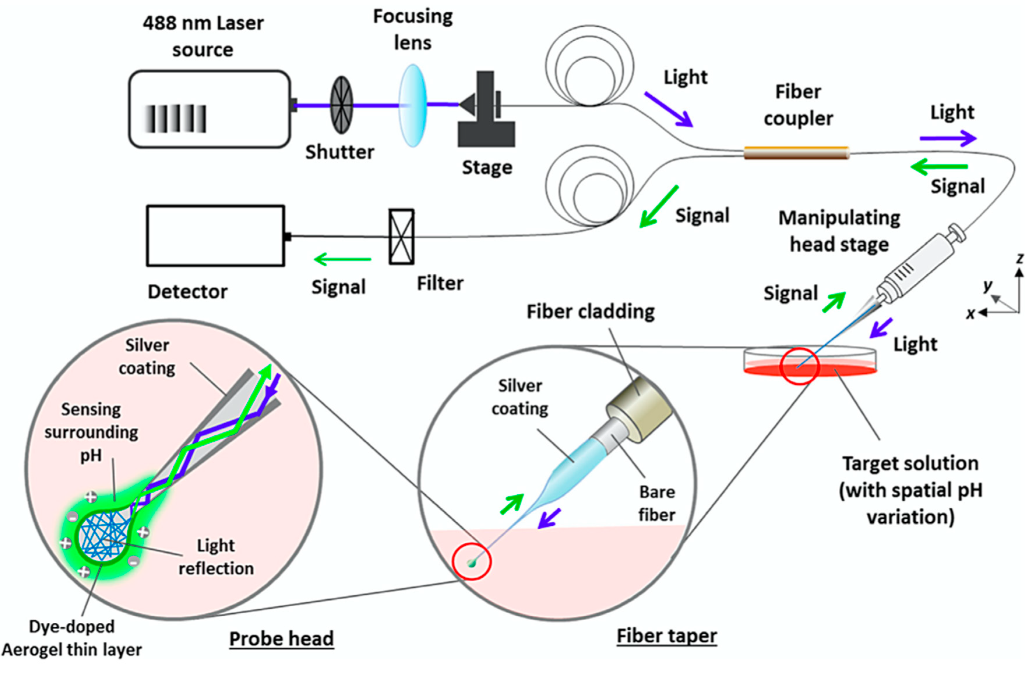
3.1.1. Fluorescence-Based Chemical Sensors

The first submicron optical fibre sensor, developed by Kopelman and co-workers in 1992 [16,124], was a pH sensor based on fluorescein as fluorescent pH indicator. The tapered fibre tip was silanised in order to provide functional groups for a photopolymerisation process (polyacrylamide layer containing the pH indicator). With this procedure, the chemical stability of the sensor was highly improved, as the polymerisation could avoid the leakage of the lipophilic fluorescein molecules from the polyacrylamide support. As proof of concept, the pH was measured in a small pore size (10 µm) of a polycarbonate membrane in buffer solution, simulating the insertion of the fibre tip into the cell. Another simple pH sensor at the tip of the fibre was obtained by Zhao et al. [125], exploiting the linear increase of the photoluminescence intensity of quantum dots (QDs) covalently immobilised onto the tip of the fibre with the increase of pH. Yang et al. [126] developed, more recently, another pH sensor onto OFT for intracellular applications. A 70 µm tapered spherical probe head was coated with fluorescent-dye doped aerogel. The dye was the pH-sensitive 2′,7′-Bis (2-carbonylethyl)-5(6)-carboxyfluorescein (BCECF), which was covalently bound within the aerogel network. The schematic diagram of the optical measurement setup is reported in Figure 2.
As for the pH sensors, several studies have also been conducted for the development of oxygen sensors at the tip of the fibre. In 1995, Rosenzweig and Kopelman developed an OFT oxygen sensor based on the fluorescence quenching of tris-(1,10-phenanthroline) ruthenium chloride by dissolved oxygen [127,128]. By following the same protocol they had developed for the realisation of the pH sensor [16], the ruthenium complex was incorporated into an acrylamide polymer layer that was covalently attached to the silanised OFT by a photopolymerisation procedure. A similar procedure was used by Jorge et al. [18], who developed an oxygen sensor based on the dynamic quenching of the fluorescence of a ruthenium complex (Tris(2,2′-bipyridine) ruthenium(II) chloride hexahydrate [Ru(bpy)3]) trapped in the porous structure of a sol–gel silica film at the tip of the fibre.
For sensors other than those for pH and oxygen, Chen et al. developed a nanotip-array for Hg2+ ion detection in buffer solution [20]. In order to increase the sensitivity of the system, a bundle of tapered fibres was functionalised instead of a single OFT, on top of which a newly synthetised thioamide–rhodamine derivative was covalently attached via silanisation. The molecule was selective and specific for Hg2+ ion, and the emitted fluorescence increased in the presence of Hg2+ owing to the ring-opening process of rhodamine derivative from spirolactam (not fluorescent) to ring-opened amide (fluorescent). The detection limit reached the micromolar range.
Another interesting application for OFTs was proposed by Wang et al., who developed sensors for intracellular Ca2+ detection [129]. The OFT was fabricated from multimode fibre with a core diameter of 200 μm by the heating and pulling method. The lateral wall of the tip was coated with silver, leaving the end of the nanosized tip uncoated. The used indicator was Calcium Green-1 Dextran, which changes its fluorescence following the complexation with Ca2+. The dye was covalently immobilised onto the tapered fibre via standard methods (silanisation and glutaraldehyde functionalisation steps). The excitation light, launched into the fibre, was at 488 nm, and the fluorescence emitted, when Calcium Green-1 Dextran chelates with Ca2+ inside the smooth muscle cell cardiomyocytes, was collected by a microscope objective and passed through a long-pass filter to be focused onto a photomultiplier for detection. The detected concentration was in the nanomolar range, which is around the physiological level of free cytosolic calcium in a single living cell (smooth muscle cell cardiomyocyte), and the response time is shorter than milliseconds. Hossein-Zadeh et al. developed an OFT applicable to intra- and extra-cellular detection of oxygen, pH, H2S, Ca2+, and acetylcholine [21]. The fibre tip was covered with aluminium thin layer (150–250 nm), except the end face of the tip. The sensing part of the tip was realised with a photocurable polymer matrix loaded with the indicator dye specific for the target molecule of interest. The role of the polymer was to provide the immobilisation sites for the indicators and to be permeable to the target molecules. Tests on the different target molecules were performed in buffer solution, even with a multifunctional probe (pH and O2 sensor), while the pH sensor was further tested in cultured neurons derived from rat cortex (intracellular testing) and in the extracellular space of brain slices obtained from mouse hippocampus (extracellular testing).
A step forward in the application of OFTs as chemical sensors was made by two different groups, which performed in vivo optical measurements of fluorescent neurons in mice and rats, using a tapered dual core optical fibre (an optical core to locally excite and collect fluorescence, and an electrolyte-filled hollow core for extracellular single unit electrophysiology). LeChasseur et al. optically measured the Ca2+ activity in a craniotomised animal by measuring the fluorescence of cortical neurons labelled using intracellular injection of Lucifer yellow [19]. Dufour et al. used the same type of dual core probe, and in vivo experiments were performed on bacterial artificial chromosome transgenic mice, where neurons were present expressing tandem dimer Tomato (tdTomato) and enhanced green fluorescent protein (eGFP) proteins under the control of the promoters for D1 and D2 dopamine receptors, respectively. Cells expressing the D1 and D2 receptors could be identified, and very few cells expressed both markers. A craniotomy was performed over the frontal part of the striatum (where dopaminergic inputs were abundant) [130].

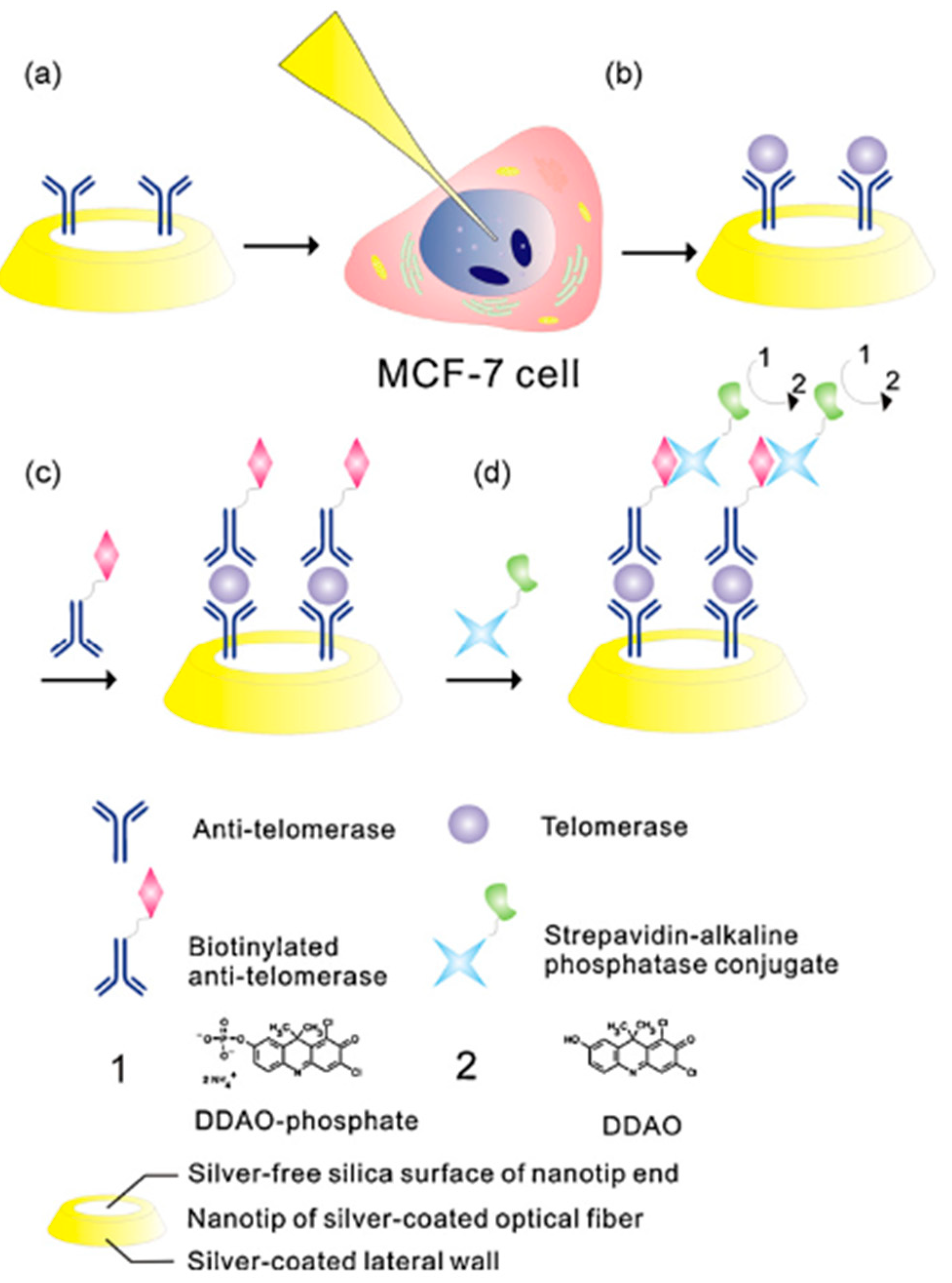
3.1.2. Fluorescence-Based Biochemical Sensors

In 1996, Rosenzweig and Kopelman [128] presented the first OFT fluorescent biosensor for glucose detection. The sensor was based on the classic enzymatic reaction for glucose detection, in which the ruthenium complex and the glucose oxidase are co-immobilised in acrylamide polymer that is covalently attached to the OFT; in the presence of glucose, glucose oxidase catalyses its oxidation to gluconic acid producing hydrogen peroxide with consume of oxygen, which is the analyte measured using the ruthenium complex. The absolute detection limit achieved was 1 × 10–15 mol with a response time of only 2 s, owing to the small size of the optical probe.
Vo-Dinh’s group reported on the use of OFT based-biosensors developed for intracellular analysis [28,32]. The tapered tip was coated with 200 nm of silver layer, preventing the coating of the sensing region; then, the tip was silanised in order to have functional groups available for antibody (anti-benzo[a]pyrene tetrol, BPT) immobilisation. The BPT was selected as a molecule of interest for cancer research, as its metabolites covalently bind to the DNA. The probe was then ready for intracellular measurements and the fibre was introduced into the cell cultured in a petri dish placed on an inverted microscope. After an equilibration of the tip into the cell lasting 5 min, the fibre was removed and placed in buffer solution. The BPT molecules, which had interacted with the specific antibodies immobilised onto the tip, were then ready to be quantified exploiting their intrinsic fluorescence, reaching a Limit of Detection (LOD) of (0.64 ± 0.17) × 10−11 M. The experiments were conducted on two different cell lines, a rat liver epithelial cell line (as control) and a human mammary carcinoma cell line. An immunoassay-based optical fibre tip was also developed by Vo-Dinh’s group for intracellular measurements of cytochrome C (a protein involved in the production of cellular energy and apoptosis) [35]. After immobilisation via silanisation of the mouse anti-cytochrome C antibody, the tip was placed inside the cell for 5 min to capture the intracellular cytochrome C. An indirect detection of the target protein was obtained by incubating the tip first in the biotinylated anti-cytochrome C antibody and then in the streptavidin-alkaline phosphatase conjugate. Finally, the nanoprobe was placed in a DDAO-phosphate solution (9H-(1,3-Dichloro-9,9-dimethylacridin-2-one-7-yl) phosphate, di-ammonium salt) for the fluorescence measurement of the cleaved DDAO.
As in the previous papers, Zheng et al. used antibody-functionalised nanotips for intracellular analysis [30]. They applied a similar preparation of the fibre; that is, the tapered tip was covered by a thin layer of silver for preventing light leakage, leaving the aperture free for optical detection; then, the sensing surface was silanised and activated with glutaraldehyde for the antibody immobilisation. In this case, the antibodies were specific for telomerase, a general cancer biomarker, and the incubation in cell was performed for 30 min and in two different cell lines (MCF-7 breast cancer cell line and human mesenchymal stem cell line, as control). The reacted telomerase at the tip of the fibre was quantified via a sandwich immunoassay (Figure 3); the nanoprobe was incubated with a biotin-labeled anti-telomerase antibody and then with a strepavidin–alkaline phosphatase conjugate; in the end, DDAO-phosphate solution was added for fluorescence measurement.
The authors demonstrated that the over-expression of telomerase in the nucleus of cancer cells was significantly higher than in the negative control, opening the way for the detection of other low expression proteins in a single living cell. In the same year, the same group of scientists applied the developed nanotip to the detection of extracellular lactate concentrations in cancer cells [33]. The lactate dehydrogenase, which catalyses lactate conversion to generate reduced nicotinamide adenine dinucleotide (NADH) for fluorescence detection, was immobilised onto the tip of the fibre, and the detection of increased extracellular lactate in cancer cell lines was demonstrated.
A step forward in the development of biosensors at the tip of the fibre for intracellular analysis was presented by Kasili et al., who performed the fluorescence measurement directly in a living cell [36]. In fact, differently from the previously described sensors in which the enzyme-linked immunosorbent assay (ELISA) for fluorescence measurements was performed out of the cell, in this work, the enzymatic reaction took place directly in the cell. The OFT was fabricated by pulling a 600 µm plastic clad silica fibre down to a final tip diameter of 50 nm; the OFT was then coated with 100 nm of silver metal. The nanotip was modified immobilising the caspase-9 substrate (leucine-glutamic acid-histidine-aspartic acid-7-amino-4-methylcoumarin (LEHD-AMC)), which is a non-fluorescent molecule. After the tip insertion in the cell (MCF-7), where apoptosis was induced and caspase-9 was consequently activated, the cleavage of the substrate was obtained and the fluorescent molecule AMC was produced. A HeCd laser (325 nm) was focused into the 600 μm delivery fibre, and the fluorescence emitted from the cells was collected by the microscope objective and sent to a photomultiplier (PMT) for detection.
Giannetti et al. developed, for the first time (to the best of our knowledge), a biosensor based on a molecular beacon (MB) immobilised onto the nanotip of a fibre [24]. MBs are single-stranded oligonucleotidic molecules that possess two complementary side-ends, promoting the formation of a stem-loop structure commonly named a hairpin structure. The loop portion of the molecule can form a double-stranded DNA by hybridisation with the complementary sequence, the target molecule. MBs can be labelled with a fluorophore and a quencher at the two side-ends of the stem, which keeps these two moieties close to each other. As the fluorophore is characterised by an emission band that overlaps the absorption band of the quencher, this proximity causes the fluorescence of the fluorophore to be quenched by energy transfer to the quencher. The fluorescence is restored upon the opening of the stem owing to the hybridisation of the MB with the target sequence [131]. In the application described here, the selected MB was specific for the messenger RNA (mRNA) coding for survivin, which is considered as a possible target for cancer diagnosis and therapy [132,133]. The MB for survivin mRNA was covalently immobilised onto the silanised tip of the fibre and labeled with ATTO647N and BlackBerry® Quencher 650 as fluorophore and quencher, respectively. Fluorescence measurements on fibre nanotips were carried out in a cuvette using a laser diode emitting at 635 nm for the MB excitation. The emitted fluorescence was collected by means of a Gradient-index (GRIN) lens coupled with a multimode optical fibre (diameter 200 μm), aligned with the fibre nanotip, then guided to an optical high-pass filter in order to block the excitation light scattered out from the fibre tip, and finally acquired by a spectrograph.
The nanotip covered with the MB was capable of monitoring increasing concentrations (from 10 nM up to 10 µm) of the specific target, showing a negligible signal increase after the interaction with the random sequence, as shown in Figure 4. In this experiment, a limit of detection of 10 nM was observed.

3.2. Optical Interrogation Systems Based on Fibre Micro/Nano Tips

Together with chemical/bio-chemical sensing, another intriguing application of OFTs is related to their use as probes for the optical interrogation of objects at nanometric scales. From Synge’s inspired intuition [134], these optical devices have made it possible to go well beyond the light diffraction limit imposed by Abbe’s criterion, laying the foundations for the development of scanning near-field optical microscopy (SNOM) technique in the mid-1980s [135,136]. The physical phenomenon behind this technique is that, by illuminating a subwavelength aperture, working as an optical probe and placed at close proximity from a sample (i.e., at a distance within the evanescent decay length of the near-field for the incident light radiation), it is possible to obtain an optical image of the scanned specimen—without scattering and diffraction effects—simply collecting the light signal after its interaction with the sample surface by means of a remote detector. As a consequence, the spatial resolution of this technique depends exclusively on the radial dimensions of the probe [9].
Hence, a SNOM system can be used to acquire super resolution optical images by scanning a probe tip over a sample surface in two or three dimensions and using the near-field component to construct the same images. The development of finely machined tips together with an accurate control mechanism for the scan procedure are the two fundamental requirements in order to improve the resolution of the overall system and to keep the probe-sample distance at a constant value—within a subwavelength domain—during the scan of the specimen surface.
In Figure 5, the working principle of a SNOM system is shown [137].

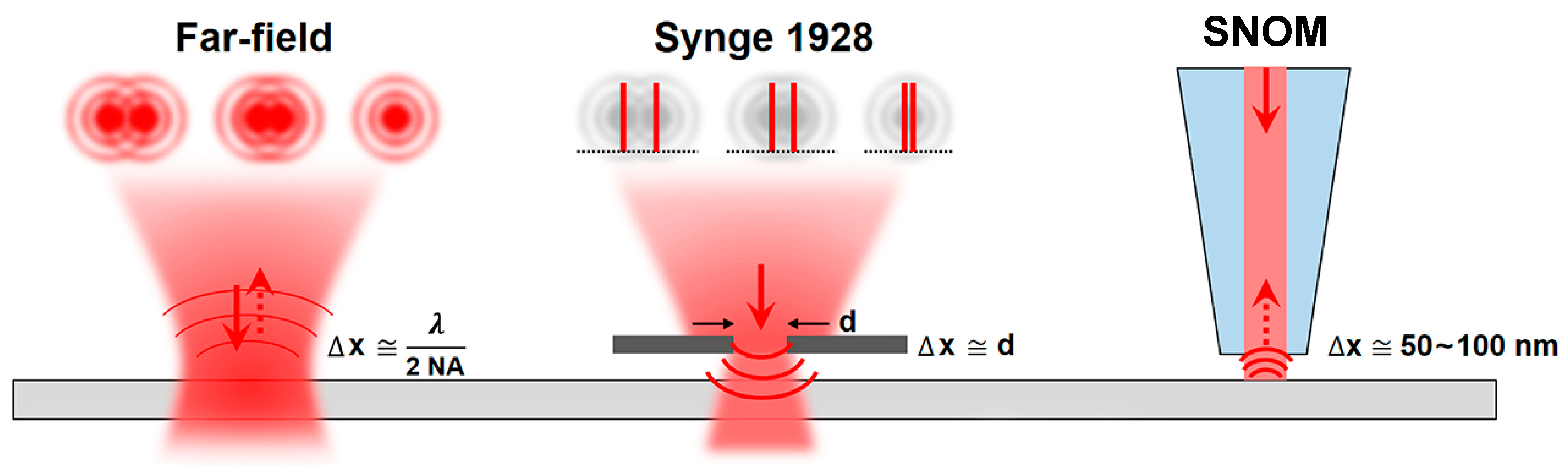
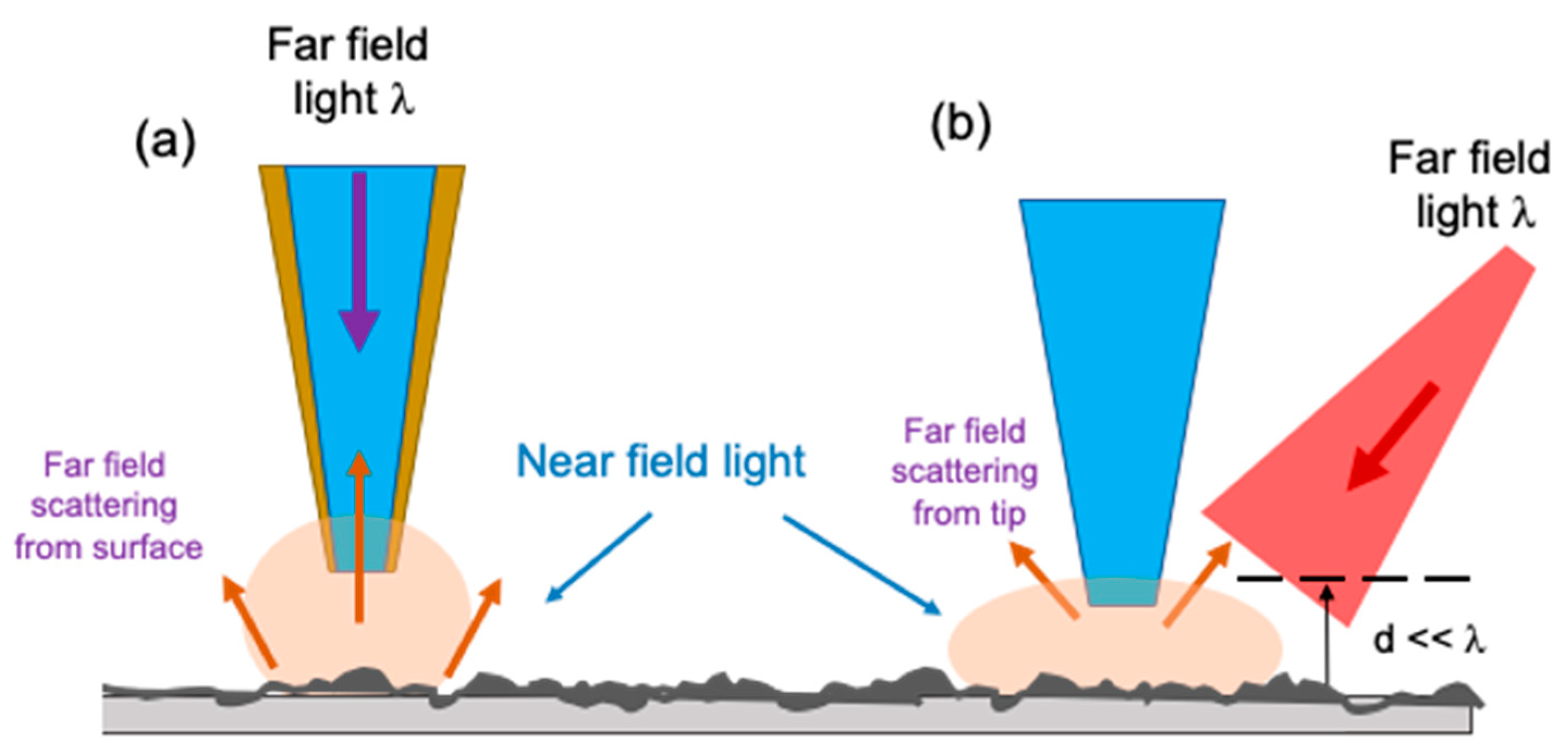
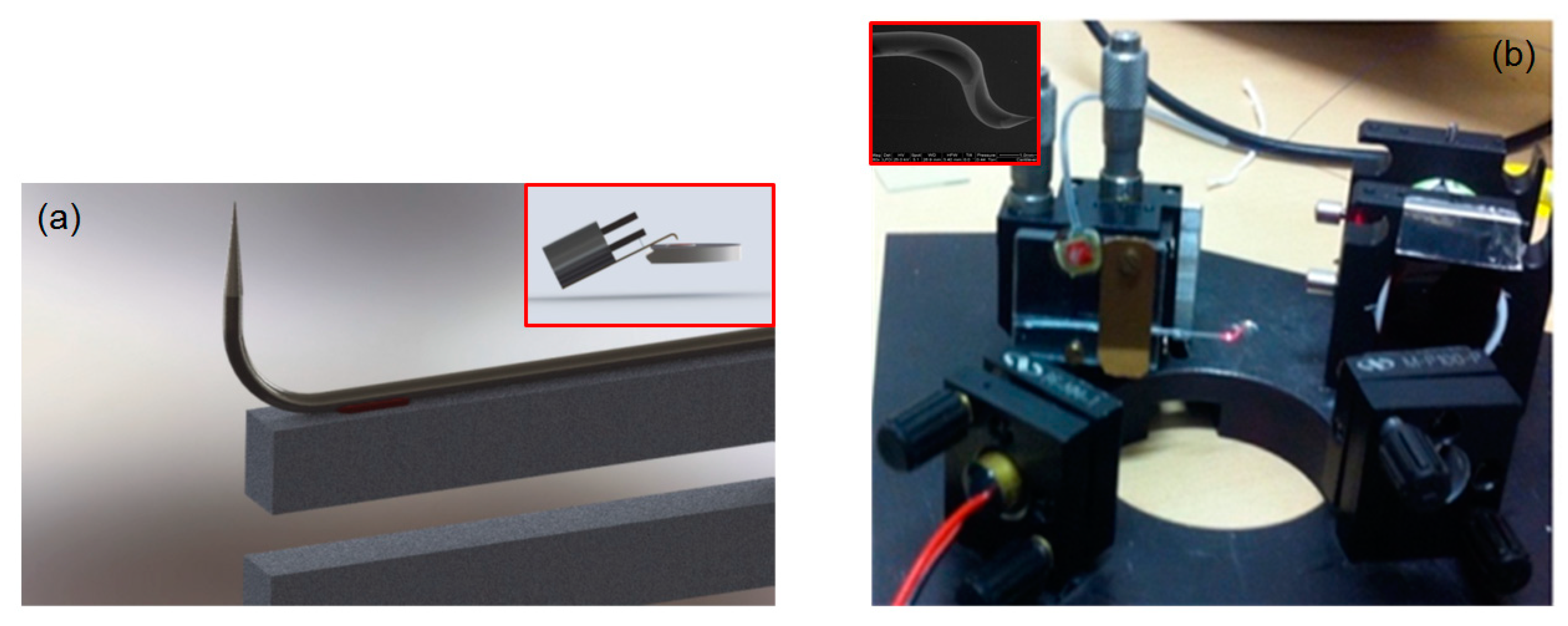
3.2.1. SNOM-Based Systems: Tip Typologies and Feedback Mechanisms

Tips with conical shape, obtained by tapering an optical fibre, are more frequently used in SNOM-based systems for both illumination and light collection [53,83,138,139], although tetrahedral or pyramidal tips have also been employed for this purpose [140,141,142].
Depending on how they are designed and realised, SNOM tips can be divided in two main classes: the so-called “aperture” ones and those defined “apertureless”. Generally, the aperture tips present a metal coating on their entire external surface except for their apex, where a nanometre portion of the original transparent material (i.e., silica in the case of a tip fabricated by tapering an optical fibre) is left uncovered. Typically, the size of this aperture is in the order of subwavelength. The presence of the thin metal film on the external wall of the tip allows a better confinement of the light signal and prevents the undesirable leakage effect of the field propagating through the tip. This type of tip can work in both “illumination” and “collection” mode. In the first operating mode, the evanescent field components at the exit of the nanoscale apex of the tip are scattered from the sample surface into the far field and then detected either in transmission or in reflection. Conversely, in the collection mode, the sample is globally illuminated by the far field coming from an external light source, and the evanescent field components are scattered by the tip—located close to the sample surface—and collected through its aperture into the fibre. Examples of optical probes belonging to this category include the tips obtained from a pulled fibre and those used in microcantilever systems [51,54]. Unlike the aperture tips, the apertureless tips present a very sharp conical shape and are made of either dielectric or metallic materials (i.e., similar to those used in AFM probes). They are able to efficiently scatter the near-field light—emitted in proximity of the illuminated sample surface—into the far field to be detected [51,143,144].
These two types of tips exhibit complementary behaviour with regard to light throughput and confinement. In particular, apertureless tips show higher light throughput, while the aperture ones guarantee a stronger light confinement ability thanks to the discontinuity in terms of material represented by metallisation. Finally, as the resolution of the system is strictly related to the size of the tip end, the best performance is obtained using the apertureless tips, which can reach a few nanometre size for their apex compared with that achievable with the aperture ones. In fact, for the latter tips, the minimum size for their aperture typically ranges from tens to hundreds of nanometers, and it is impossible to go further down due to the skin depth of their metallic coating. Nevertheless, despite their better performance, the apertureless tips have a more intense far-field background noise, which makes them less usable from a practical point of view compared with the aperture ones [9,51].
Figure 6 reports the working principle of these two types of optical nanotips generally used in SNOM systems.
As already mentioned, together with the type of tip used, in a SNOM system, it is important to have a feedback mechanism capable of keeping constant—below the wavelength of the excitation light—the distance of the sample surface from the tip during its scanning. In this context, the main methods adopted to control the probe-sample distance are the so-called shear-force mechanism (SFM) based on tuning fork and lateral force control [145,146,147,148], the normal force feedback as used in AFM mode [149,150,151,152], and that based on tunnelling phenomena as adopted in the scanning tunnelling microscopy (STM) [153,154,155].
The SFM/SNOM generally adopts aperture probes directly obtained by tapering an optical fibre. The feedback mechanism is realised by fixing this optical probe to one arm of the quartz tuning fork, whose shape and operating mode are the same as that of its musical counterpart (also said diapason). An electrical circuit is used to drive its lateral oscillation, also being able to acquire the feedback signal. As the tip of the optical fibre interacts with the sample, the oscillation is softened owing to the presence of the shear forces. The resulting measured effect becomes a parameter to be inserted in the control electronics in order to adjust the height of the optical fibre tip by means of a piezoelectric scanner [145,146,147,148].
The AFM-based SNOM systems (AFM/SNOM) make use of cantilevers and metal or metal-coated tips, directly fixed to the end of the same cantilever. The operating mode most widely used by these systems is the so-called “tapping” mode, in which the cantilever is oscillated, around its resonance frequency, by a piezoelectric device. The swing direction is normal to the sample surface. Different interaction forces come into play when the tip approaches the sample (i.e., Van der Waals forces, dipole–dipole interactions, electrostatic forces). The presence of these forces causes a change in the oscillation amplitude of the cantilever. This amplitude is used as an input parameter of a feedback control electronics, which drives a vertical actuator through which the height of the cantilever, with respect to the sample, is controlled. In this way, the oscillation amplitude of the cantilever is kept constant during the scan and, consequently, the mean height of the tip/sample distance is also constant. The deflection of the cantilever is measured using a laser beam reflected from the top of the same microlever towards a matrix of photodiodes [149,150,151,152].
Finally, in the case of the STM/SNOM system, the control electronics measures the tunneling current flowing between the metallic probe and the conducting sample. Moreover, the same control unit acts to keep this parameter at a constant value, by sending appropriate electrical signals to a piezoelectric ceramic device, which changes the XYZ position of the tip with respect to the sample. The value of these signals represents a kind of height map of the sample surface. A typical STM mechanics allows performing suitable displacement with sub-nanometre resolution in the vertical and horizontal direction. In order to have a good spatial resolution, the STM/SNOM systems adopt metal probes with apertureless apex as small as possible (i.e., an atom) [153,154,155].
Once the distance is carefully controlled by one of these feedback mechanisms, the probe performs a raster scan on the sample plane in order to simultaneously acquire the optical and topographic signals at each position on the sample surface and then reconstruct the corresponding maps. Table 2 shows the main characteristics of these approaches, with their relative advantages and disadvantages.
Among the methods listed above, the one based on the SFM/SNOM makes the most use of aperture/apertureless probes directly obtained by tapering an optical fibre. However, this approach presents a complicate operating mode and a low resolution owing to the lateral force mechanism. In order to overcome the limitations imposed by this method in terms of resolution, an interesting alternative involves the use of a modified AFM/SNOM configuration exploiting the best performance of the feedback mechanism based on the normal force control (i.e., “tapping” mode) typical of the AFM systems.
In the first configuration, the fibre is bent near the tip and connected to the tuning fork system [156]. Moreover, in order to obtain a truly “tapping” character for the tip motion (comparable to that of a cantilever-based AFM system), dithering and short lengths for the freestanding part of the bent fibre probe are requested in both double-resonant condition and the non-resonant one [64,157].
As an alternative to this solution, short fragments of optical fibre—opportunely shaped—can be employed in order to directly exploit the tapping mode of an AFM/SNOM system. In this context, the authors demonstrated the possibility to obtain optical fibre nanotips by the Wing method (WM), and subsequently bend it by an arc discharge process generally available on board of a common splicing machine [158]. Moreover, the bending point of the nanotip was made reflective thanks to a lapping abrasive method. The so-fabricated nanotool was mounted on a classical OBD (optical beam detection) system in place of the AFM cantilever. Then, a laser spot was focalised on the reflecting area of the fibre nanotip and the resulting reflected light was collected by a four-quadrant detector. The achieved signal level was enough to detect the nanotip movements and to follow its oscillations when excited by a small piezo at around its natural frequency, as it is usually performed in a classical AFM/SNOM microscope. Figure 7 shows the core of these two AFM/SNOM strategies.
As an example of the application of SNOM systems based on fibre micro/nanotips, we will overview in the next paragraph the interesting case of topographic and near field analysis of particular optical devices such as whispering gallery mode microresonators.

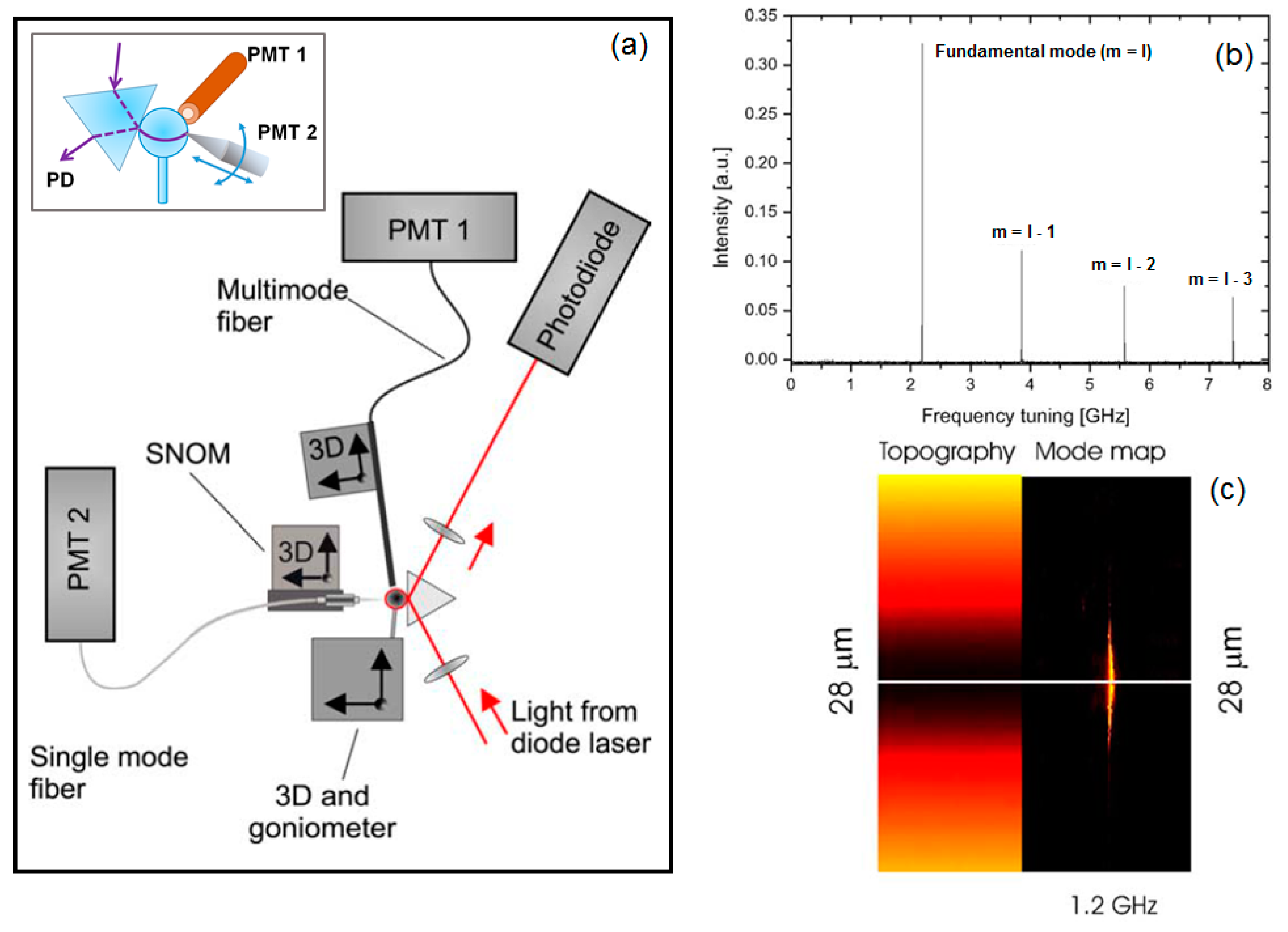
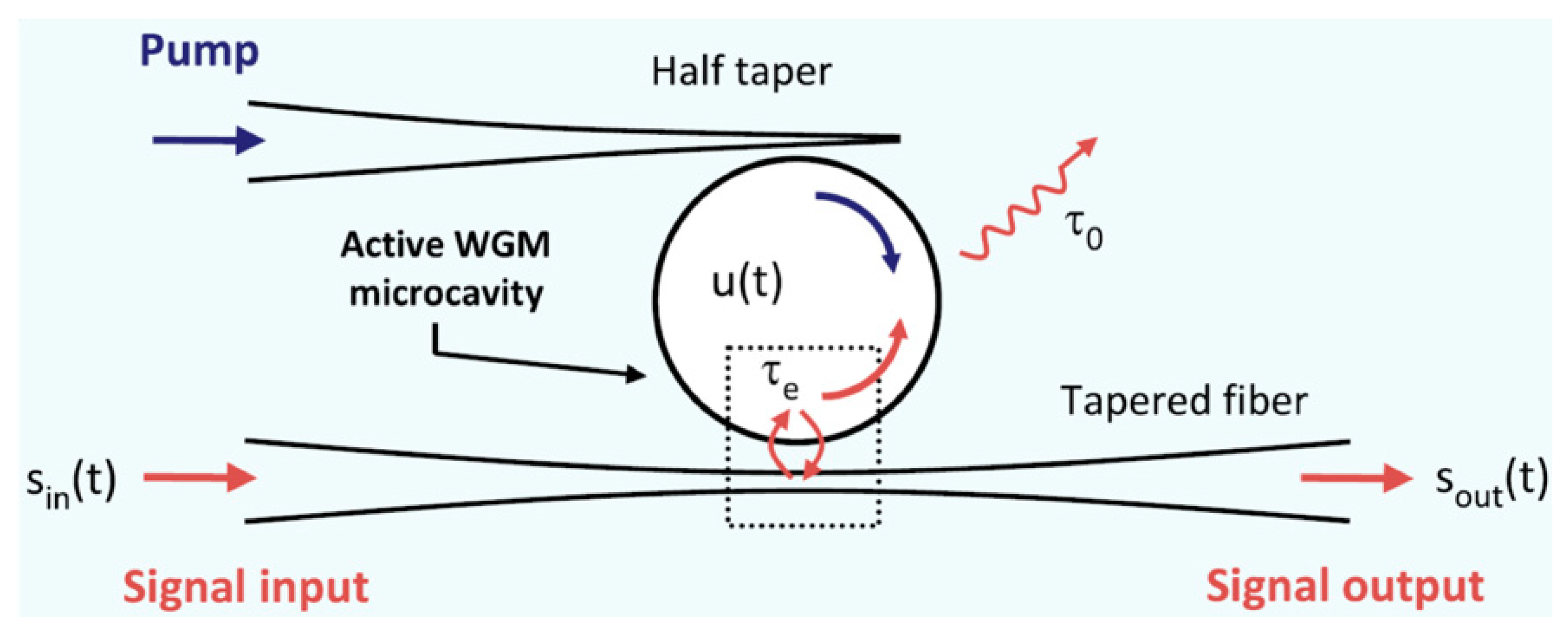
3.2.2. Optical Fibre Micro/Nanotips as Near-Field Probe and Coupler in Whispering Gallery Mode (WGM) Resonators

Fibre optical micro/nanotips represent useful tools as near-field probes for spatially mapping the intensity distribution of whispering gallery modes (WGMs) supported by the high Q-factor microcavities [158,159,160,161,162,163,164]. The original idea was presented for the first time by J. C. Knight et al. in 1995, envisaging the use of a tip with sub-micrometric size (typically, hundreds of nanometres), realised on the head of a single mode optical fibre, able to move close to the surface of a fused silica microsphere along a meridian in order to map the angular dependence of the WGMs [77]. The method was based on the evanescent field and tunneling mechanisms occurring at the microresonator surface, for both the WGM excitation (i.e., in this case, by means of a mono-mode side polished fibre) and their detection by a nanotip. The nanotip, with its subwavelength-sized numerical aperture, was able to collect the information carried by the WGM evanescent waves near the resonator surface and convert it into propagating waves along the same optical fibre (that on which the nanotip was made), connected to a photodiode. The lock-in amplifier provided the signal-to-noise ratio increase and the electronic locking of the laser with the resonance. The overall system was driven by a Personal Computer for the movement control, data acquisition, and elaboration.
After a few years, this approach was first adopted and improved by M.L.M. Balistreri et al. [78], and subsequently by S. Gotzinger and co-workers [79], in order to not only map the WGM intensity distribution, but also derive important information on the surface topography and the geometrical characteristics (i.e., the effective size and eccentricity) of the microresonator under investigation. For this purpose, the authors controlled the reciprocal distance d between the nanotip and the WGM optical microcavity (d ~10 nm) no longer with a piezoelectric positioning system, but via the shear-force mechanism commonly used in the SNOM technique [58,59,68]. This conferred the system a greater stability, guaranteeing the possibility to scan the microresonator surface at a constant distance with extremely high precision. In the same way, the nanometric size of the tip aperture and the feedback of the shear-force mechanism conferred to the overall system a high optical and topographical resolution, respectively. The same authors demonstrated that the presence of a SNOM nanotip, close to the WGM resonator surface and located in correspondence of the evanescent field of a selected WGM (e.g., the fundamental one), could perturb the spatial position of that resonant mode within the cavity and contribute to reducing the Q factor as a result of increased scattering losses. Nevertheless, if the fibre tip was sharp enough (<100 nm), the scattering contribution could be considered negligible, and the Q factor remained almost unchanged, even when the tip distance from the WGMR surface was about 10 nm [165]. This result paved the way for establishing well-controlled light coupling conditions to a certain WGM of the microcavity, as reported by Mazzei and co-workers [80,81]. The sketch of the improved experimental set-up together with the main achieved results is shown in Figure 8. The light beam coming from a tunable laser diode was focused by a lens on the prism surface. A WGM microsphere was opportunely positioned close to the base of the prism by means of a 3D translational and rotating stage. WGMs of the microsphere were excited by total internal reflection occurring at the base of the prism coupler only for a discrete set of the incidence angles that the laser beam formed with the normal at the input face of the prism. A multimode optical fibre, connected with a photomultiplier (PMT1), was used to collect the scattered light and register the WGMs spectrum represented by a set of equally spaced modes belonging to the same family (i.e., those having the same angular mode number l, but different azimuthal mode number m) together with the fundamental one (m = l).
At the same time, the SNOM tip, obtained by pulling a commercial optical fibre, was connected to another photomultiplier (PMT2) with the aim to detect the signal mapping during its scan mode in the polar direction around the equatorial plane of the spherical microresonator, as sketched in the inset of Figure 8a. By optimizing the coupling condition with respect to the fundamental WGM by means of the topographical and mode mapping information, it was possible to detect the WGMs’ spectrum (see Figure 8b) in which the fundamental mode is clearly stronger than the other resonant modes (ml) and, simultaneously, to acquire its topographical and spatial-spectral mode map as reported in the left side and right side of Figure 8c, respectively.
Moreover, using the same optical set-up reported in Figure 8a, the authors demonstrated how the fibre nanotip can be used to simulate the presence of a nanoparticle in a certain position of the microresonator surface. The presence of this scattering element plays a key role in the coherent coupling between clockwise (cw) and counterclockwise (ccw) resonator WGMs. In particular, when the fibre nanotip is far enough away from a mode (i.e., the fundamental one), the coupling is very weak and a single peak resonance is appreciable at the photomultiplier (PMT1) level. As the scatterer approaches the evanescent field of the selected mode, the coupling regime becomes weak and the resonance broadening occurs owing to the enhanced incoherent scattering phenomenon. Finally, moving the fibre nanotip further towards the mode intensity maximum, the coupling regime between the cw and ccw propagating modes gradually increases until exceeding the inhomogeneous losses, and consequently assuming a coherent characteristic. When this condition is verified, a mode splitting is observed at the photomultiplier (PMT1). These two peaks correspond to two symmetric and anti-symmetric eigenmodes that represent standing waves given by the linear combination of waves propagating in opposite directions [81]. The phenomenon described above is the basis of one of the sensing mechanisms, called precisely mode splitting, which is generally used for the detection of nanoparticles (i.e., metal ions as water pollutants) by means of these optical WGM microcavities [166].
Other interesting results in terms of mode mapping have been experimentally obtained on disk WGMRs by different research groups. However, in these cases, the authors used a SNOM system combined with a commercial AFM metal nanotip as a probe for their experiments. This goes beyond the subject of this review, which is focused on the use of optical micro/nano tips directly fabricated at the end of an optical fibres. For further details on this approach, please refer to the literature [167,168,169].
Besides the possibility of mapping the spatial distribution of the WGMs in resonant micro-resonators, the use of fibre tips can also serve to excite/extract the light radiation in/out the WGM cavity. Differently from the previous case, where the fibre tip is generally placed with a certain angle of inclination near the surface of the microresonator and moved along the meridian (polar) direction in order to map the angular dependence of the mode patterns for different resonance modes (as occurs, for instance, in the case of a microsphere), here, the fibre tip is positioned tangentially to the resonant cavity surface and close to its equatorial plane. The light coupling is based again on the evanescent field and tunneling mechanisms occurring at the microresonator surface between the WGMs supported by the resonant cavity and the mode propagating through the interrogation system.
A detailed analysis of the light coupling mechanism in a WGM resonant cavity by means of fibre tip, in the form of a half-tapered fibre with few micrometres size, was recently presented and discussed by Bhadkamkar and co-workers [170]. In their work, the authors also considered some geometrical parameters, like the shape and the diameter of the fibre tip, together with the separation distance and the coupling length, in order to optimize the phase matching condition and the coupling efficiency. They demonstrated that, for a fibre tip of 1.5 μm in diameter and a coupling length of 10 μm, the coupled power is around 30%.
Another example of application that uses a fibre tip for coupling light into a WGM cavity is described by Rasoloniaina et al. [171], who employed a half-tapered fibre to couple the pump signal in a glass microsphere, doped with erbium ions, in order to selectively control the coupling regime, from undercoupling to amplification condition, by changing the pump rate in the fibre tip, and measured the related ringdown signal in the cavity. A second tapered fibre, positioned close to the equatorial plane of the microcavity and diametrically opposed to the fibre tip, was adopted to inject/extract the light signal in/out the same active microcavity. The overall system represents a three-port device, as sketched in Figure 9.
Differently, Pham and co-workers used two half-tapered fibres with a waist diameter of 1 μm and a tip angle of 0.72° to couple the pump signal at 980 nm in an Erbium-doped silica microsphere and extract the resulting laser output in a wide wavelength range from 1510 nm to 1580 nm. The authors demonstrated that, adjusting opportunely the gap between the extraction fibre tip and the microsphere surface, it was possible not only to change from multi-mode lasing operation to a single-mode one, but also to select a desired single-mode regime among several. The spacing gap should be more than 150 nm in order to prevent the effect of the dipole–field interaction between the fibre tip and the cavity surface, which can confer mechanical instability to the same half-tapered extraction fibre [172].
Recently, fibre micro/nano tips have been used for light coupling in WGM microdroplets. Generally, this class of liquid WGMRs was optically interrogated by a free space technique, which involved a tightly focusing of the light beam, coming from a tuneable laser source, tangentially to the microdroplet rim. In this case, both the transmitted and scattered signals were monitored with a coupling efficiency of around 6% [173,174]. An alternative to the WGM excitation in a liquid microdroplet was to exploit the near field approach based on the evanescent field of the mode propagating in a tapered fibre, located close to the droplet surface and grazing its equatorial plane. Only the transmitted signal was checked and, by opportunely controlling the air gap between the taper and the droplet, a coupling efficiency higher than 50% was demonstrated [175].
Together with the strategies mentioned above, some research groups exploited an optical fibre micro/nano tip, thermally pulled from a standard single-mode fibre, to transmit the pump light and excite a fluorescent dye-doped liquid crystal microdroplet with the aim to produce a lasing action for sensing applications [176,177,178]. The small size and the strong evanescent field intensity of the excitation beam at the output of the micro/nano tip, owing to the reshaping effect of the tapered fibre on the single mode propagating along it, allowed the optical coupling with the WGMs supported by these active microcavities. In this way, the broadband fluorescence spectrum was modulated by the different WGMs of the liquid microresonator, thus generating a typical comb signal. The lasing emission spectra of dye-doped microdroplets were collected by a microscope objective with high numerical aperture. The pump light was removed by a suitable filter. The signal so filtered was made available to a CCD camera and a spectrometer. The occurrence of a chemical/biochemical binding event, or the simple modification of the chemical/physical characteristic of the environment where the WGM microcavity was located, caused a shift of the comb. From the measurement of this shift, it was possible to trace the magnitude of the quantity (i.e., chemical, physical, biological) under investigation. Figure 10a sketches the core of the experimental set-up adopted for monitoring the pH change in a penicillinase enzymatic reaction with nematic liquid crystal (LC) 4-cyano-4′-pentylbiphenyl (5CB) microdroplet, doped with 4′-pentyl-biphenyl-4-carboxylic acid (PBA). The pump light, coming from a pulsed laser at a wavelength of 532 nm, was coupled to the LC microdroplet. The resulting fluorescence and lasing spectra, collected by a spectrometer at the output of a high numerical microscope objective (not shown in the Figure 10), such as the LC orientation of the microcavity, proved to be sensitive to the pH change of the surrounding environment in which the microdroplet was inserted. Consequently, a red-shift of the WGM comb spectra was observed in response to the pH variation (see Figure 10b) [178]. On the basis of this result, the authors demonstrated that the changes in the WGM lasing spectra associated with microdroplet configuration transitions can indeed serve as an indicator of the H+ released from the penicillinase enzymatic reaction.

4. Conclusions and Perspectives

OFT applications, introduced and discussed in this work, show how this kind of nanotool is highly spread in different research fields, from biochemical sensors up to photonic devices. Moreover, the Wing fabrication method (WM) has shown a great potential to forge these optical nanodevices. Their realisation has revolutionised the technology of optical fibres at the nanoscale level, allowing the achievement of new and intriguing applications.
Considering, for instance, the possibility of studying individual cells and their biochemical composition at a high spatial resolution, as well as monitoring their response over time to any external stimuli directly in their natural environment, it is possible to shed light on several intracellular phenomena, including the comprehension of the main mechanisms related to some diseases at cellular level. In such intracellular sensing applications, it should be not forgotten that the tip dimension becomes an extremely stringent factor in order not to damage the cell membrane and excessively perturb its energy system. For this purpose, dimensions well below one hundred nanometres are generally required. This makes the so-obtained nanoprobe extremely fragile from a mechanical point of view and, at the same time, the related intracellular sensing becomes a very challenging task.
Conversely, applications as biochemical sensors for micro and nanoenvironments are straightforward, but in this case, the challenge is to reach a lower limit of detection than other competitive techniques.
In photonics, nowadays, there is a growing interest for the micro/nanotips as either optical tweezers or coupling devices, and a larger spreading should be expected in the future for these applications. In particular, the use of multimode optical fibres for the realisation of these nanoprobes can pave the way to the achievement of multifunctional capabilities such as imaging, sensing, and nanoparticles’ manipulation in a same optical device.
Furthermore, while AFM and SNOM applications are well known and can be considered as “gold standard” in many research fields, TERS and SERS techniques are still evolving and deserve a deeper attention in order to develop standardised procedures. In all these cases, there is a considerable research effort towards the achievement of optical nanoprobes having an even stronger spatial confinement for the light signal, in order to guarantee high spatial resolution (~few nanometres), high light intensity, and field amplitude at the apex tip. Different strategies can be adopted to achieve this goal, involving the excitation and propagation of surface plasmon polaritons (SPPs) in metallic and/or metal-coated fibre nanotips [179], the exploitation of enhanced nonlinear optical effects [180], or the interfacing with plasmonic nanoconcentrators at the end of the fibre tip [39]. These new approaches represent excellent candidates for the development in the near future of nanoscale imaging and spectroscopy, including scanning quantum spin spectroscopy and scanning thermal imaging microscopy.

Author Contributions

Conceptualization, S.B., A.B., and A.G.; methodology, A.B., S.B., A.G., F.C., S.T., and C.T.; software, A.B., C.T., F.Q., and B.T.; validation, A.B., S.B., A.G., and F.C.; formal analysis, A.B., C.T., A.G., B.T., and F.Q.; investigation, A.B., S.B., A.G., C.T., S.T., B.T., F.Q., S.P., and F.B.; resources, A.G., S.T., F.C., B.T., and F.Q.; data curation, A.B., C.T., and A.G.; writing—original draft preparation, S.B., A.B., and A.G.; writing—review and editing, A.B., S.B., A.G., C.T., S.T., F.B., and G.C.R.; visualization, S.B., A.G., and A.B.; supervision, A.G. and S.B.; project administration, A.G. and S.B.; funding acquisition, A.G. and S.B. All authors have read and agreed to the published version of the manuscript.

Funding

This research was partially funded by the European Community and the Tuscany Region (Italy) within the framework of the SAFE WATER project (Horizon 2020 Research&Innovation program and the ERA-NET “PhotonicSensing” cofund -G.A.No 688735); partially by the European Community and the Tuscany Region (Italy) within the framework of the FASPEC project (Horizon 2020—PhotonicSensing ERA-NET COFUND; G. A. 688735); and partially by Fondazione Cassa di Risparmio di Firenze for the DECODE project.

Conflicts of Interest

The authors declare no conflict of interest.

References

  1. Krishnamoorthy, A.V.; Thacker, H.D.; Torudbakken, O.; Muller, S.; Srinivasan, A.; Decker, P.J.; Opheim, H.; Cunningham, J.E.; Shubin, I.; Zheng, X.; et al. From chip to cloud: Optical interconnects in engineered systems. J. Light. Technol. 2017, 35, 3103–3115. [Google Scholar] [CrossRef]
  2. Richardson, D.J. New optical fibres for high-capacity optical communications. Philos. Trans. R. Soc. A Math. Phys. Eng. Sci. 2016, 374. [Google Scholar] [CrossRef] [PubMed] [Green Version]
  3. Pospíšilová, M.; Kuncová, G.; Trögl, J. Fiber-optic chemical sensors and fiber-optic bio-sensors. Sensors 2015, 15, 25208–25259. [Google Scholar] [CrossRef] [PubMed]
  4. Li, J.; Ebendorff-Heidepriem, H.; Gibson, B.C.; Greentree, A.D.; Hutchinson, M.R.; Jia, P.; Kostecki, R.; Liu, G.; Orth, A.; Ploschner, M.; et al. Perspective: Biomedical sensing and imaging with optical fibers—Innovation through convergence of science disciplines. APL Photonics 2018, 3, 100902. [Google Scholar] [CrossRef]
  5. Vukolov, K.Y. Fiber optics for plasma diagnostics in ITER. Fusion Eng. Des. 2017, 123, 919–922. [Google Scholar] [CrossRef]
  6. N’cho, J.S.; Fofana, I. Review of fiber optic diagnostic techniques for power transformers. Energies 2020, 13, 1789. [Google Scholar] [CrossRef] [Green Version]
  7. Brambilla, G. Optical fibre nanowires and microwires: A review. J. Opt. A Pure Appl. Opt. 2010, 12, 043001. [Google Scholar] [CrossRef]
  8. Tong, L. Micro/nanofibre optical sensors: Challenges and prospects. Sensors 2018, 18, 903. [Google Scholar] [CrossRef] [Green Version]
  9. Paiva, J.S.; Jorge, P.A.S.; Rosa, C.C.; Cunha, J.P.S. Optical fiber tips for biological applications: From light confinement, biosensing to bioparticles manipulation. Biochim. Biophys. Acta-Gen. Subj. 2018, 1862, 1209–1246. [Google Scholar] [CrossRef]
  10. Decombe, J.-B.; Huant, S.; Fick, J. Single and dual fiber nano-tip optical tweezers: Trapping and analysis. Opt. Express 2013, 21, 30521. [Google Scholar] [CrossRef] [Green Version]
  11. Ribeiro, R.S.R.; Soppera, O.; Oliva, A.G.; Guerreiro, A.; Jorge, P.A.S. New trends on optical fiber tweezers. J. Light. Technol. 2015, 33, 3394–3405. [Google Scholar] [CrossRef]
  12. Li, Y.; Xin, H.; Xu, X.; Liu, X.; Li, B. Fibre-optic trapping and manipulation at the nanoscale. Adv. Mater. Lett. 2018, 9, 567–577. [Google Scholar] [CrossRef]
  13. Zhang, Y.; Dobson, P.S.; Weaver, J.M.R. High temperature imaging using a thermally compensated cantilever resistive probe for scanning thermal microscopy. J. Vac. Sci. Technol. B Nanotechnol. Microelectron. Mater. Process. Meas. Phenom. 2012, 30, 010601. [Google Scholar] [CrossRef]
  14. Liscio, A.; Palermo, V.; Samorì, P. Nanoscale quantitative measurement of the potential of charged nanostructures by electrostatic and Kelvin probe force microscopy: Unraveling electronic processes in complex materials. Acc. Chem. Res. 2010, 43, 541–550. [Google Scholar] [CrossRef]
  15. André, R.M.; Warren-Smith, S.C.; Becker, M.; Dellith, J.; Rothhardt, M.; Zibaii, M.I.; Latifi, H.; Marques, M.B.; Bartelt, H.; Frazão, O. Tapered optical fiber tip probes based on focused ion beam-milled Fabry-Perot microcavities. Nanoeng. Fabr. Prop. Opt. Devices XIII 2016, 9927, 99270R. [Google Scholar]
  16. Tan, W.; Shi, Z.Y.; Kopelman, R. Development of submicron chemical fiber optic sensors. Anal. Chem. 1992, 64, 2985–2990. [Google Scholar] [CrossRef]
  17. Liu, Y.H.; Dam, T.H.; Pantano, P. A pH-sensitive nanotip array imaging sensor. Anal. Chim. Acta 2000, 419, 215–225. [Google Scholar] [CrossRef]
  18. Jorge, P.A.S.; Caldas, P.; Rosa, C.C.; Oliva, A.G.; Santos, J.L. Optical fiber probes for fluorescence based oxygen sensing. Sens. Actuators B Chem. 2004, 103, 290–299. [Google Scholar] [CrossRef] [Green Version]
  19. Lechasseur, Y.; Dufour, S.; Lavertu, G.; Bories, C.; Deschênes, M.; Vallée, R.; De Koninck, Y. A microprobe for parallel optical and electrical recordings from single neurons in vivo. Nat. Methods 2011, 8, 319–325. [Google Scholar] [CrossRef]
  20. Chen, K.; Adam, C.; Sojic, N.; Schmittel, M. Photochemical functionalisation of optical nanotips with a rhodamine chemosensor for remote through-fiber detection of Hg2+. RSC Adv. 2013, 3, 24140–24145. [Google Scholar] [CrossRef]
  21. Hossein-Zadeh, M.; Delgado, J.; Schweizer, F.; Lieberman, R. Sub-micron opto-chemical probes for studying living neurons. Neural Imaging Sens. 2017, 10051, 100510G. [Google Scholar]
  22. Gao, H.H.; Chen, Z.; Kumar, J.; Tripathy, S.K.; Kaplan, D.L. Tapered fiber tips for fiber optic biosensors. Opt. Eng. 1995, 34, 3465–3470. [Google Scholar] [CrossRef]
  23. Barucci, A.; Berneschi, S.; Cosi, F.; Nunzi Conti, G.; Pelli, S.; Quercioli, F.; Soria, S.; Righini, G.C. Fiber optic nanoprobes for biological sensing. In Proceedings of the 22nd Congress of the International Commission for Optics: Light for the Development of the World, Puebla, Mexico, 2 November 2011; Volume 8011, p. 80118X. [Google Scholar]
  24. Giannetti, A.; Barucci, A.; Cosi, F.; Pelli, S.; Tombelli, S.; Trono, C.; Baldini, F. Optical fiber nanotips coated with molecular beacons for DNA detection. Sensors 2015, 15, 9666–9680. [Google Scholar] [CrossRef] [Green Version]
  25. Vo-Dinh, T.; Zhang, Y. Single-cell monitoring using fiberoptic nanosensors. Wiley Interdiscip. Rev. Nanomed. Nanobiotechnol. 2011, 3, 79–85. [Google Scholar] [CrossRef]
  26. Zhang, Y.; Dhawan, A.; Vo-Dinh, T. Design and fabrication of fiber-optic nanoprobes for optical sensing. Nanoscale Res. Lett. 2012, 7, 6–18. [Google Scholar] [CrossRef] [Green Version]
  27. Vo-Dinh, T. Nanobiosensors: Probing the sanctuary of individual living cells. J. Cell. Biochem. 2002, 87, 154–161. [Google Scholar] [CrossRef]
  28. Vo-Dinh, T.; Alarie, J.P.; Cullum, B.M.; Griffin, G.D. Antibody-based nanoprobe for measurement of a fluorescent analyte in a single cell. Nat. Biotechnol. 2000, 18, 764–767. [Google Scholar] [CrossRef]
  29. Vo-Dinh, T.; Griffin, G.D.; Alarie, J.P.; Cullum, B.; Sumpter, B.; Noid, D. Development of nanosensors and bioprobes. J. Nanopart. Res. 2000, 2, 17–27. [Google Scholar] [CrossRef]
  30. Zheng, X.T.; Li, C.M. Single living cell detection of telomerase over-expression for cancer detection by an optical fiber nanobiosensor. Biosens. Bioelectron. 2010, 25, 1548–1552. [Google Scholar] [CrossRef]
  31. Vo-Dinh, T.; Kasili, P. Fiber-optic nanosensors for single-cell monitoring. Anal. Bioanal. Chem. 2005, 382, 918–925. [Google Scholar] [CrossRef] [PubMed]
  32. Cullum, B.M.; Griffin, G.D.; Miller, G.H.; Vo-Dinh, T. Intracellular measurements in mammary carcinoma cells using fiber-optic nanosensors. Anal. Biochem. 2000, 277, 25–32. [Google Scholar] [CrossRef]
  33. Zheng, X.T.; Yang, H.B.; Li, C.M. Optical detection of single cell lactate release for cancer metabolic analysis. Anal. Chem. 2010, 82, 5082–5087. [Google Scholar] [CrossRef]
  34. Barker, S.L.R.; Kopelman, R.; Meyer, T.E.; Cusanovich, M.A. Fiber-optic nitric oxide-selective biosensors and nanosensors. Anal. Chem. 1998, 70, 971–976. [Google Scholar] [CrossRef]
  35. Song, J.M.; Kasili, P.M.; Griffin, G.D.; Vo-Dinh, T. Detection of Cytochrome c in a single cell using an optical nanobiosensor. Anal. Chem. 2004, 76, 2591–2594. [Google Scholar] [CrossRef]
  36. Kasili, P.M.; Song, J.M.; Vo-Dinh, T. Optical sensor for the detection of caspase-9 activity in a single cell. J. Am. Chem. Soc. 2004, 126, 2799–2806. [Google Scholar] [CrossRef]
  37. Vo-Dinh, T.; Kasili, P.; Wabuyele, M. Nanoprobes and nanobiosensors for monitoring and imaging individual living cells. Nanomed. Nanotechnol. Biol. Med. 2006, 2, 22–30. [Google Scholar] [CrossRef]
  38. Kasili, P.M.; Vo-Dinh, T. Optical nanobiosensor for monitoring an apoptotic signaling process in a single living cell following photodynamic therapy. J. Nanosci. Nanotechnol. 2005, 5, 2057–2062. [Google Scholar] [CrossRef]
  39. Tuniz, A.; Schmidt, M.A. Interfacing optical fibers with plasmonic nanoconcentrators. Nanophotonics 2018, 7, 1279–1298. [Google Scholar] [CrossRef]
  40. Uebel, P.; Bauerschmidt, S.T.; Schmidt, M.A.; Russell, P.S.J. A gold-nanotip optical fiber for plasmon-enhanced near-field detection. Appl. Phys. Lett. 2013, 103, 021101. [Google Scholar] [CrossRef] [Green Version]
  41. Auwärter, D.; Mihaljevic, J.; Meixner, A.J.; Zimmermann, C.; Slama, S. Coupling of optical far fields into apertureless plasmonic nanofiber tips. Phys. Rev. A—At. Mol. Opt. Phys. 2013, 88, 1–6. [Google Scholar] [CrossRef] [Green Version]
  42. Sciacca, B.; Monro, T.M. Dip biosensor based on localized surface plasmon resonance at the tip of an optical fiber. Langmuir 2014, 30, 946–954. [Google Scholar] [CrossRef]
  43. Viets, C.; Hill, W. Fibre-optic SERS sensors with angled tips. J. Mol. Struct. 2001, 565, 515–518. [Google Scholar] [CrossRef]
  44. Chen, Z.; Dai, Z.; Chen, N.; Liu, S.; Pang, F.; Lu, B.; Wang, T. Gold nanoparticles-modified tapered fiber nanoprobe for remote SERS detection. IEEE Photonics Technol. Lett. 2014, 26, 777–780. [Google Scholar] [CrossRef]
  45. Liu, S.; Huang, J.; Chen, Z.; Chen, N.; Pang, F.; Wang, T.; Hu, L. Raman spectroscopy measurement of levofloxacin lactate in blood using an optical fiber nano-probe. J. Raman Spectrosc. 2015, 46, 197–201. [Google Scholar] [CrossRef]
  46. Morozov, Y.M.; Lapchuk, A.S.; Prygun, A.V.; Kryuchyn, A.A.; Dostalek, J. Investigation of optical fiber-tip probes for common and ultrafast SERS. New J. Phys. 2020, 22, 033027. [Google Scholar] [CrossRef]
  47. Jin, D.; Bai, Y.; Chen, H.; Liu, S.; Chen, N.; Huang, J.; Huang, S.; Chen, Z. SERS detection of expired tetracycline hydrochloride with an optical fiber nano-probe. Anal. Methods 2015, 7, 1307–1312. [Google Scholar] [CrossRef]
  48. Roth, R.M.; Panoiu, N.C.; Adams, M.M.; Osgood, R.M.; Neacsu, C.C.; Raschke, M.B. Resonant-plasmon field enhancement from asymmetrically illuminated conical metallic-probe tips. Opt. Express 2006, 14, 2921. [Google Scholar] [CrossRef]
  49. Le Nader, V.; Mevellec, J.Y.; Minea, T.; Louarn, G. Gold nanoparticles as probes for nano-Raman spectroscopy: Preliminary experimental results and modeling. Int. J. Opt. 2012. [Google Scholar] [CrossRef]
  50. Stadler, J.; Schmid, T.; Zenobi, R. Developments in and practical guidelines for tip-enhanced Raman spectroscopy. Nanoscale 2012, 4, 1856–1870. [Google Scholar] [CrossRef]
  51. Bazylewski, P.; Ezugwu, S.; Fanchini, G. A review of three-dimensional scanning near-field optical microscopy (3D-SNOM) and its applications in nanoscale light management. Appl. Sci. 2017, 7, 973. [Google Scholar] [CrossRef] [Green Version]
  52. Tugchin, B.N.; Janunts, N.; Klein, A.E.; Steinert, M.; Fasold, S.; Diziain, S.; Sison, M.; Kley, E.B.; Tünnermann, A.; Pertsch, T. Plasmonic tip based on excitation of radially polarized conical surface plasmon polariton for detecting longitudinal and transversal fields. ACS Photonics 2015, 2, 1468–1475. [Google Scholar] [CrossRef]
  53. Yang, J.; Zhang, J.; Li, Z.; Gong, Q. Fabrication of high-quality SNOM probes by pre-treating the fibres before chemical etching. J. Microsc. 2007, 228, 40–44. [Google Scholar] [CrossRef] [PubMed]
  54. Hecht, B.; Sick, B.; Wild, U.P.; Deckert, V.; Zenobi, R.; Martin, O.J.F.; Pohl, D.W. Scanning near-field optical microscopy with aperture probes: Fundamentals and applications. J. Chem. Phys. 2000, 112, 7761–7774. [Google Scholar] [CrossRef]
  55. Essaidi, N.; Chen, Y.; Kottler, V.; Cambril, E.; Mayeux, C.; Ronarch, N.; Vieu, C. Fabrication and characterization of optical-fiber nanoprobes for scanning near-field optical microscopy. Appl. Opt. 1998, 37, 609. [Google Scholar] [CrossRef]
  56. Kim, S.; Yu, N.; Ma, X.; Zhu, Y.; Liu, Q.; Liu, M.; Yan, R. High external-efficiency nanofocusing for lens-free near-field optical nanoscopy. Nat. Photonics 2019, 13, 636–643. [Google Scholar] [CrossRef]
  57. Janunts, N.A.; Baghdasaryan, K.S.; Nerkararyan, K.V.; Hecht, B. Excitation and superfocusing of surface plasmon polaritons on a silver-coated optical fiber tip. Opt. Commun. 2005, 253, 118–124. [Google Scholar] [CrossRef]
  58. Karrai, K.; Grober, R.D. Piezoelectric tip-sample distance control for near field optical microscopes. Appl. Phys. Lett. 1995, 66, 1842–1844. [Google Scholar] [CrossRef]
  59. Durkan, C.; Shvets, I.V. Study of shear force as a distance regulation mechanism for scanning near-field optical microscopy. J. Appl. Phys. 1996, 79, 1219–1223. [Google Scholar] [CrossRef]
  60. Muramatsu, H.; Chiba, N.; Yamamoto, N.; Homma, K.; Ataka, T.; Shigeno, M.; Monobe, H.; Fujihira, M. Multi-functional SNOM/AFM probe with accurately controlled low spring constant. Ultramicroscopy 1998, 71, 73–79. [Google Scholar] [CrossRef]
  61. David, T.; Chicanne, C.; Richard, N.; Krenn, J.R.; Scheurer, F.; Ounadjela, K.; Hehn, M.; Lacroute, Y.; Goudonnet, J.P. Application to dielectric, metallic, and magnetic samples of a transmission mode scanning near field optical microscope with normal force distance regulation on bent optical fibers. Rev. Sci. Instrum. 1999, 70, 4587–4594. [Google Scholar] [CrossRef]
  62. Chimmalgi, A.; Hwang, D.J.; Grigoropoulos, C.P. Nanoscale rapid melting and crystallization of semiconductor thin films. Nano Lett. 2005, 5, 1924–1930. [Google Scholar] [CrossRef] [PubMed]
  63. Gonzalez, L.; Martínez-Martín, D.; Otero, J.; de Pablo, P.J.; Puig-Vidal, M.; Gómez-Herrero, J. Improving the lateral resolution of quartz tuning fork-based sensors in liquid by integrating commercial AFM tips into the fiber end. Sensors 2015, 15, 1601–1610. [Google Scholar] [CrossRef] [PubMed] [Green Version]
  64. Smirnov, A.; Yasinskii, V.M.; Filimonenko, D.S.; Rostova, E.; Dietler, G.; Sekatskii, S.K. True tapping mode scanning near-field optical microscopy with bent glass fiber probes. Scanning 2018. [Google Scholar] [CrossRef] [PubMed] [Green Version]
  65. Tiribilli, B.; Margheri, G.; Baschieri, P.; Menozzi, C.; Chavan, D.; Iannuzzi, D. Fibre-top atomic force microscope probe with optical near-field detection capabilities. J. Microsc. 2011, 242, 10–14. [Google Scholar] [CrossRef]
  66. Higbie, J. Microscope resolution. Am. J. Phys. 1981, 49, 40–42. [Google Scholar] [CrossRef]
  67. Small, A. Spherical aberration, coma, and the Abbe sine condition for physicists who don’t design lenses. Am. J. Phys. 2018, 86, 487–494. [Google Scholar] [CrossRef]
  68. Sandoghdar, V.; Wegscheider, S.; Krausch, G.; Mlynek, J. Reflection scanning near-field optical microscopy with uncoated fiber tips: How good is the resolution really? J. Appl. Phys. 1997, 81, 2499–2503. [Google Scholar] [CrossRef]
  69. Choo, A.G.; Jackson, H.E.; Thiel, U.; De Brabander, G.N.; Boyd, J.T. Near field measurements of optical channel waveguides and directional couplers. Appl. Phys. Lett. 1994, 65, 947–949. [Google Scholar] [CrossRef]
  70. Bourzeix, S.; Moison, J.M.; Mignard, F.; Barthe, F.; Boccara, A.C.; Licoppe, C.; Mersali, B.; Allovon, M.; Bruno, A. Near-field optical imaging of light propagation in semiconductor waveguide structures. Appl. Phys. Lett. 1998, 73, 1035–1037. [Google Scholar] [CrossRef]
  71. Vohnsen, B.; Bozhevolnyi, S.I. Comment on “local observations of phase singularities in optical fields in waveguide structures”. Phys. Rev. Lett. 2001, 87, 259401. [Google Scholar] [CrossRef]
  72. Balistreri, M.L.M.; Driessen, A.; Korterik, J.P.; Kuipers, L.; van Hulst, N.F. Quasi interference of perpendicularly polarized guided modes observed with a photon scanning tunneling microscope. Opt. Lett. 2000, 25, 637. [Google Scholar] [CrossRef] [PubMed] [Green Version]
  73. Chicanne, C.; Emonin, S.; Richard, N.; David, T.; Bourillot, E.; Goudonnet, J.P.; Lacroute, Y. Characterization of optogeometric parameters of optical fibers by near-field scanning probe microscopies. J. Opt. Soc. Am. B 2000, 17, 1473. [Google Scholar] [CrossRef]
  74. Nesci, A.; Fainman, Y. Complex amplitude of an ultrashort pulse in a waveguide measured with a coherent, femtosecond resolution NSOM at 1550 nm. In Proceedings of the 16th Annual Meeting of the IEEE Lasers and Electro-Optics Society LEOS 2003, Tucson, AZ, USA, 27 October 2003; Volume 1, pp. 49–50. [Google Scholar]
  75. Abashin, M.; Tortora, P.; Märki, I.; Levy, U.; Nakagawa, W.; Vaccaro, L.; Herzig, H.P.; Fainman, Y. Near-field characterization of propagating optical modes in photonic crystal waveguides. Opt. Express 2006, 14, 1643. [Google Scholar] [CrossRef] [PubMed] [Green Version]
  76. Bozhevolnyi, S.I.; Kuipers, L. Near-field characterization of photonic crystal waveguides. Semicond. Sci. Technol. 2006, 21, R1. [Google Scholar] [CrossRef] [Green Version]
  77. Knight, J.C.; Dubreuil, N.; Sandoghdar, V.; Hare, J.; Lefèvre-Seguin, V.; Raimond, J.M.; Haroche, S. Mapping whispering-gallery modes in microspheres with a near-field probe. Opt. Lett. 1995, 20, 1515. [Google Scholar] [CrossRef]
  78. Balistreri, M.L.; Klunder, D.J.; Blom, F.C.; Driessen, A.; Hoekstra, H.W.; Korterik, J.P.; Kuipers, L.; van Hulst, N.F. Visualizing the whispering gallery modes in a cylindrical optical microcavity. Opt. Lett. 1999, 24, 1829. [Google Scholar] [CrossRef]
  79. Götzinger, S.; Demmerer, S.; Benson, O.; Sandoghdar, V. Mapping and manipulating whispering gallery modes of a microsphere resonator with a near-field probe. J. Microsc. 2001, 202, 117–121. [Google Scholar] [CrossRef] [Green Version]
  80. Mazzei, A.; Götzinger, S.; Menezes, L.D.S.; Sandoghdar, V.; Benson, O. Optimization of prism coupling to high-Q modes in a microsphere resonator using a near-field probe. Opt. Commun. 2005, 250, 428–433. [Google Scholar] [CrossRef]
  81. Mazzei, A.; Götzinger, S.; Menezes, D.S.; Zumofen, G.; Benson, O.; Sandoghdar, V. Controlled coupling of counterpropagating Whispering-Gallery modes by a single rayleigh scatterer: A classical problem in a quantum optical light. Phys. Rev. Lett. 2007, 99, 1–4. [Google Scholar] [CrossRef] [Green Version]
  82. Valaskovic, G.A.; Holton, M.; Morrison, G.H. Parameter control, characterization, and optimization in the fabrication of optical fiber near-field probes. Appl. Opt. 1995, 34, 1215. [Google Scholar] [CrossRef]
  83. Sayah, A.; Philipona, C.; Lambelet, P.; Pfeffer, M.; Marquis-Weible, F. Fiber tips for scanning near-field optical microscopy fabricated by normal and reverse etching. Ultramicroscopy 1998, 71, 59–63. [Google Scholar] [CrossRef]
  84. Stöckle, R.; Fokas, C.; Deckert, V.; Zenobi, R.; Sick, B.; Hecht, B.; Wild, U.P. High-quality near-field optical probes by tube etching. Appl. Phys. Lett. 1999, 75, 160–162. [Google Scholar] [CrossRef]
  85. Wan, M.M.; Menon, P.S.; Sahbudin, S. Microfabricated fiber probe by combination of electric arc discharge and chemical etching techniques. Adv. Mater. Res. 2012, 462, 38–41. [Google Scholar]
  86. Demagh, N.E.; Guessoum, A.; Aissat, H. Chemical etching of concave cone fibre ends for core fibre alignment. Meas. Sci. Technol. 2006, 17, 119–122. [Google Scholar] [CrossRef]
  87. Rickelt, L.F.; Ottosen, L.D.M.; Kühl, M. Etching of multimode optical glass fibers: A new method for shaping the measuring tip and immobilization of indicator dyes in recessed fiber-optic microprobes. Sens. Actuators B Chem. 2015, 211, 462–468. [Google Scholar] [CrossRef] [Green Version]
  88. Tao, M.; Jin, Y.; Gu, N.; Huang, L. A method to control the fabrication of etched optical fiber probes with nanometric tips. J. Opt. A Pure Appl. Opt. 2010, 12, 1–5. [Google Scholar] [CrossRef]
  89. Okayama, T.; Seki, H. Fabrication and evaluation of silica-based optical fiber probes by chemical etching method. Opt. Rev. 2005, 12, 25–28. [Google Scholar] [CrossRef]
  90. Hoffmann, P.; Dutoit, B.; Salathé, R.P. Comparison of mechanically drawn and protection layer chemically etched optical fiber tips. Ultramicroscopy 1995, 61, 165–170. [Google Scholar] [CrossRef]
  91. Lazarev, A.; Fang, N.; Luo, Q.; Zhang, X. Formation of fine near-field scanning optical microscopy tips. Part I. By static and dynamic chemical etching. Rev. Sci. Instrum. 2003, 74, 3679–3683. [Google Scholar] [CrossRef] [Green Version]
  92. Gu, N.; Li, C.A.; Sun, L.; Liu, Z.H.; Sun, Y.K.; Xu, L.N. Controllable fabrication of fiber nano-tips by dynamic chemical etching based on siphon principle. J. Vac. Sci. Technol. B Microelectron. Nanom. Struct. 2004, 22, 2283–2285. [Google Scholar] [CrossRef]
  93. Barucci, A.; Cosi, F.; Giannetti, A.; Pelli, S.; Griffini, D.; Insinna, M.; Salvadori, S.; Tiribilli, B.; Righini, G.C. Optical fibre nanotips fabricated by a dynamic chemical etching for sensing applications. J. Appl. Phys. 2015, 117, 053104. [Google Scholar] [CrossRef]
  94. Griffini, D.; Insinna, M.; Salvadori, S.; Barucci, A.; Cosi, F.; Pelli, S.; Righini, G.C. On the CFD analysis of a stratified taylor-couette system dedicated to the fabrication of nanosensors. Fluids 2017, 2, 8. [Google Scholar] [CrossRef] [Green Version]
  95. Vaiano, P.; Carotenuto, B.; Pisco, M.; Ricciardi, A.; Quero, G.; Consales, M.; Crescitelli, A.; Esposito, E.; Cusano, A. Lab on Fiber Technology for biological sensing applications. Laser Photonics Rev. 2016, 10, 922–961. [Google Scholar] [CrossRef]
  96. Rodrigues Ribeiro, R.S.; Dahal, P.; Guerreiro, A.; Jorge, P.; Viegas, J. Optical fibers as beam shapers: From Gaussian beams to optical vortices. Opt. Lett. 2016, 41, 2137. [Google Scholar] [CrossRef] [PubMed]
  97. Meingailis, J. Focused ion beam technology and applications. J. Vac. Sci. Technol. B 1987, 5, 469–495. [Google Scholar] [CrossRef]
  98. Bassim, N.; Scott, K.; Giannuzzi, L.A. Recent advances in focused ion beam technology and applications. MRS Bull. 2014, 39, 317–325. [Google Scholar] [CrossRef] [Green Version]
  99. Micco, A.; Ricciardi, A.; Pisco, M.; La Ferrara, V.; Cusano, A. Optical fiber tip templating using direct focused ion beam milling. Sci. Rep. 2015, 5, 15935. [Google Scholar] [CrossRef]
  100. Kang, S.; Joe, H.E.; Kim, J.; Jeong, Y.; Min, B.K.; Oh, K. Subwavelength plasmonic lens patterned on a composite optical fiber facet for quasi-one-dimensional Bessel beam generation. Appl. Phys. Lett. 2011, 98, 97–99. [Google Scholar] [CrossRef]
  101. Mivelle, M.; Ibrahim, I.A.; Baida, F.; Burr, G.W.; Nedeljkovic, D.; Charraut, D.; Rauch, J.-Y.; Salut, R.; Grosjean, T. Bowtie nano-aperture as interface between near-fields and a single-mode fiber. Opt. Express 2010, 18, 15964. [Google Scholar] [CrossRef]
  102. André, R.M.; Pevec, S.; Becker, M.; Dellith, J.; Rothhardt, M.; Marques, M.B.; Donlagic, D.; Bartelt, H.; Frazão, O. Focused ion beam post-processing of optical fiber Fabry-Perot cavities for sensing applications. Opt. Express 2014, 22, 13102. [Google Scholar] [CrossRef]
  103. Kim, J.K.; Kim, J.; Oh, K.; Sohn, I.B.; Shin, W.; Choi, H.Y.; Lee, B. Fabrication of micro fresnel zone plate lens on a mode-expanded hybrid optical fiber using a femtosecond laser ablation system. IEEE Photonics Technol. Lett. 2009, 21, 21–23. [Google Scholar] [CrossRef]
  104. Rao, Y.J.; Ran, Z.L. Optic fiber sensors fabricated by laser-micromachining. Opt. Fiber Technol. 2013, 19, 808–821. [Google Scholar] [CrossRef]
  105. Wei, T.; Han, Y.; Tsai, H.-L.; Xiao, H. Miniaturized fiber inline Fabry-Perot interferometer fabricated with a femtosecond laser. Opt. Lett. 2008, 33, 536. [Google Scholar] [CrossRef]
  106. Frazão, O.; Caldas, P.; Santos, J.L.; Marques, P.V.S.; Turck, C.; Lougnot, D.J.; Soppera, O. Fabry-Perot refractometer based on an end-of-fiber polymer tip. Opt. Lett. 2009, 34, 2474. [Google Scholar] [CrossRef]
  107. Jradi, S.; Soppera, O.; Lougnot, D.J. Fabrication of polymer waveguides between two optical fibers using spatially controlled light-induced polymerization. Appl. Opt. 2008, 47, 3987–3993. [Google Scholar] [CrossRef]
  108. Soppera, O.; Jradi, S.; Lougnot, D.J. Photopolymerization with microscale resolution: Influence of the physico-chemical and photonic parameters. J. Polym. Sci. Part A Polym. Chem. 2008, 46, 3783–3794. [Google Scholar] [CrossRef]
  109. Bachelot, R.; Ecoffet, C.; Deloeil, D.; Royer, P.; Lougnot, D.-J. Integration of micrometer-sized polymer elements at the end of optical fibers by free-radical photopolymerization. Appl. Opt. 2001, 40, 5860–5871. [Google Scholar] [CrossRef]
  110. Bachelot, R.; Fares, A.; Fikri, R.; Barchiesi, D.; Lerondel, G.; Royer, P. Coupling semiconductor lasers into single-mode optical fibers by use of tips grown by photopolymerization. Opt. Lett. 2004, 29, 1971. [Google Scholar] [CrossRef]
  111. Kim, J.; Lee, S.; Jeong, Y.; Kim, J.-K.; Jung, Y.; Merenda, F.; Salathè, R.-P.; Shin, J.-S.; Oh, K. Crossed fiber optic Bessel beams for curvilinear optofluidic transport of dielectric particles. Opt. Express 2013, 21, 23021. [Google Scholar] [CrossRef]
  112. Jradi, S.; Balan, L.; Zeng, X.H.; Plain, J.; Lougnot, D.J.; Royer, P.; Bachelot, R.; Akil, S.; Soppera, O.; Vidal, L. Spatially controlled synthesis of silver nanoparticles and nanowires by photosensitized reduction. Nanotechnology 2010, 21, 1–7. [Google Scholar] [CrossRef]
  113. Ton, X.A.; Bui, B.T.S.; Resmini, M.; Bonomi, P.; Dika, I.; Soppera, O.; Haupt, K. A versatile fiber-optic fluorescence sensor based on molecularly imprinted microstructures polymerized in situ. Angew. Chem. 2013, 52, 8317–8321. [Google Scholar] [CrossRef]
  114. Pisco, M.; Galeotti, F.; Quero, G.; Iadicicco, A.; Giordano, M.; Cusano, A. Miniaturized sensing probes based on metallic dielectric crystals self-assembled on optical fiber tips. ACS Photonics 2014, 1, 917–927. [Google Scholar] [CrossRef]
  115. Novotny, L.; Pohl, D.W.; Hecht, B. Scanning near-field optical probe with ultrasmall spot size. Opt. Lett. 1995, 20, 970. [Google Scholar] [CrossRef]
  116. Betzig, E.; Trautman, J.K.; Harris, T.D.; Weiner, J.S.; Kostelak, R.L. Breaking the diffraction barrier: Optical microscopy on a nanometric scale. Science 1991, 251, 1468–1470. [Google Scholar] [CrossRef]
  117. Foti, A.; D’Andrea, C.; Bonaccorso, F.; Lanza, M.; Calogero, G.; Messina, E.; Maragò, O.M.; Fazio, B.; Gucciardi, P.G. A shape-engineered surface-enhanced raman scattering optical fiber sensor working from the visible to the near-infrared. Plasmonics 2013, 8, 13–23. [Google Scholar] [CrossRef]
  118. Vo-Dinh, T.; Scaffidi, J.; Gregas, M.; Zhang, Y.; Seewaldt, V. Applications of fiber-optics-based nanosensors to drug discovery. Expert Opin. Drug Discov. 2009, 4, 889–900. [Google Scholar] [CrossRef]
  119. Vo-Dinh, T. Nanosensing at the single cell level. Spectrochim. Acta—Part B At. Spectrosc. 2008, 63, 95–103. [Google Scholar] [CrossRef] [Green Version]
  120. Lu, J.; Rosenzweig, Z. Nanoscale fluorescent sensors for intracellular analysis. Fresenius. J. Anal. Chem. 2000, 366, 569–575. [Google Scholar] [CrossRef]
  121. Tai, Y.-H.; Wei, P.-K. Sensitive liquid refractive index sensors using tapered optical fiber tips. Opt. Lett. 2010, 35, 944. [Google Scholar] [CrossRef]
  122. Stoddart, P.R.; White, D.J. Optical fibre SERS sensors. Anal. Bioanal. Chem. 2009, 394, 1761–1774. [Google Scholar] [CrossRef]
  123. Scaffidi, J.P.; Gregas, M.K.; Seewaldt, V.; Vo-Dinh, T. SERS-based plasmonic nanobiosensing in single living cells. Anal. Bioanal. Chem. 2009, 393, 1135–1141. [Google Scholar] [CrossRef] [Green Version]
  124. Tan, W.; Shi, Z.Y.; Smith, S.; Birnbaum, D.; Kopelman, R. Submicrometer intracellular chemical optical fiber sensors. Science 1992, 258, 778–781. [Google Scholar] [CrossRef] [Green Version]
  125. Zhao, F.; Kim, I.; Kim, J. Fabrication of the optical fiber pH sensor based on CdSe/ZnS quantum dot. J. Nanosci. Nanotechnol. 2014, 14, 5650–5653. [Google Scholar] [CrossRef]
  126. Yang, Q.; Wang, H.; Lan, X.; Cheng, B.; Chen, S.; Shi, H.; Xiao, H.; Ma, Y. Reflection-mode micro-spherical fiber-optic probes for in vitro real-time and single-cell level pH sensing. Sens. Actuators B Chem. 2015, 207, 571–580. [Google Scholar] [CrossRef] [Green Version]
  127. Rosenzweig, Z.; Kopelman, R. Development of a submicrometer optical fiber oxygen sensor. Anal. Chem. 1995, 67, 2650–2654. [Google Scholar] [CrossRef]
  128. Rosenzweig, Z.; Kopelman, R. Analytical properties of miniaturized oxygen and glucose fiber optic sensor. Sens. Actuators B. Chem. 1996, 35–36, 475–483. [Google Scholar] [CrossRef]
  129. Wanga, S.; Ye, F.; Lang, X.; Fei, D.; Ge, Y.; Turner, A.P.F. Detection of [Ca2+]i changes in sub-plasma membrane microdomains in a single living cell by an optical fiber-based nanobiosensor. Austin J. Nanomed. Nanotechnol. 2014, 2, 1022. [Google Scholar]
  130. Dufour, S.; Lavertu, G.; Dufour-Beauséjour, S.; Juneau-Fecteau, A.; Calakos, N.; Deschênes, M.; Vallée, R.; De Koninck, Y. A multimodal micro-optrode combining field and single unit recording, multispectral detection and photolabeling capabilities. PLoS ONE 2013, 8, e57703. [Google Scholar] [CrossRef] [Green Version]
  131. Giannetti, A.; Tombelli, S.; Baldini, F. Oligonucleotide optical switches for intracellular sensing optical nanosensing in cells. Anal. Bioanal. Chem. 2013, 405, 6181–6196. [Google Scholar] [CrossRef]
  132. Carpi, S.; Fogli, S.; Giannetti, A.; Adinolfi, B.; Tombelli, S.; Da Pozzo, E.; Vanni, A.; Martinotti, E.; Martini, C.; Breschi, M.C.; et al. Theranostic properties of a survivin-directed molecular beacon in human melanoma cells. PLoS ONE 2014, 9, e114588. [Google Scholar] [CrossRef] [Green Version]
  133. Adinolfi, B.; Pellegrino, M.; Giannetti, A.; Tombelli, S.; Trono, C.; Sotgiu, G.; Varchi, G.; Ballestri, M.; Posati, T.; Carpi, S.; et al. Molecular beacon-decorated polymethylmethacrylate core-shell fluorescent nanoparticles for the detection of survivin mRNA in human cancer cells. Biosens. Bioelectron. 2017, 88, 15–24. [Google Scholar] [CrossRef]
  134. Synge, E.H. A suggested method for extending microscopic resolution into the ultra-microscopic region. Philos. Mag. Ser. 7 XXXVIII 1928, 6, 356–362. [Google Scholar] [CrossRef]
  135. Lewis, A.; Isaacson, M.; Harootunian, A.; Muray, A. Development of a 500 Å spatial resolution light microscope. I. light is efficiently transmitted through λ/16 diameter apertures. Ultramicroscopy 1984, 13, 227–231. [Google Scholar] [CrossRef]
  136. Pohl, D.W.; Denk, W.; Lanz, M. Optical stethoscopy: Image recording with resolution λ/20. Appl. Phys. Lett. 1984, 44, 651–653. [Google Scholar] [CrossRef]
  137. Lee, H.; Lee, D.Y.; Kang, M.G.; Koo, Y.; Kim, T.; Park, K. Tip-enhanced photoluminescence nano-spectroscopy and nano-imaging. Nanophotonics 2020. [Google Scholar] [CrossRef]
  138. Bogdanowicz, J.; Gilbert, M.; Koelling, S.; Vandervorst, W. Impact of the apex of an elongated dielectric tip upon its light absorption properties. Appl. Surf. Sci. 2014, 302, 223–225. [Google Scholar] [CrossRef]
  139. Thu, N.T.; Tanaka, K.; Tanaka, M.; Chien, D.N. Superfocusing of surface plasmon polaritons by metal-coated dielectric probe of tilted conical shape. J. Opt. Soc. Am. A 2013, 30, 1113. [Google Scholar] [CrossRef] [PubMed]
  140. Tanaka, K.; Burr, G.W.; Grosjean, T.; Maletzky, T.; Fischer, U.C. Superfocussing in a metal-coated tetrahedral tip by dimensional reduction of surface-to edge-plasmon modes. Appl. Phys. B Lasers Opt. 2008, 93, 257–266. [Google Scholar] [CrossRef]
  141. Fischer, U.C.; Koglin, J.; Fuchs, H. The tetrahedral tip as probe for scanning near-field optical microscopy at 30 nm resolution. J. Microsc. 1994, 176, 231–237. [Google Scholar] [CrossRef]
  142. Wang, X.Q.; Wu, S.F.; Jian, G.S.; Pan, S. The advantages of a pyramidal probe tip entirely coated with a thin metal film for SNOM. Phys. Lett. Sect. A Gen. At. Solid State Phys. 2003, 319, 514–517. [Google Scholar] [CrossRef]
  143. Sandoghdar, V.; Mlynek, J. Prospects of apertureless SNOM with active probes. J. Opt. A Pure Appl. Opt. 1999, 1, 523–530. [Google Scholar] [CrossRef]
  144. Bek, A.; Vogelgesang, R.; Kern, K. Apertureless scanning near field optical microscope with sub- 10 nm resolution. Rev. Sci. Instrum. 2006, 77, 043703. [Google Scholar] [CrossRef] [Green Version]
  145. Betzig, E.; Finn, P.L.; Weiner, J.S. Combined shear force and near-field scanning optical microscopy. Appl. Phys. Lett. 1992, 60, 2484–2486. [Google Scholar] [CrossRef]
  146. Shang, G.Y.; Wang, C.; Wu, J.; Bai, C.L.; Lei, F.H. Shear force scanning near-field optical microscope based on a piezoelectric bimorph cantilever. Rev. Sci. Instrum. 2001, 72, 2344–2349. [Google Scholar] [CrossRef]
  147. Gao, F.; Li, X.; Wang, J.; Fu, Y. Dynamic behavior of tuning fork shear-force structures in a SNOM system. Ultramicroscopy 2014, 142, 10–23. [Google Scholar] [CrossRef]
  148. Gao, F.; Li, X. Research on the sensing performance of the tuning fork-probe as a micro interaction sensor. Sensors 2015, 15, 24530–24552. [Google Scholar] [CrossRef]
  149. Schürmann, G.; Noell, W.; Staufer, U.; De Rooij, N.F. Microfabrication of a combined AFM-SNOM sensor. Ultramicroscopy 2000, 82, 33–38. [Google Scholar] [CrossRef]
  150. Grabiec, P.; Gotszalk, T.; Radojewski, J.; Edinger, K.; Abedinov, N.; Rangelow, I.W. SNOM/AFM microprobe integrated with piezoresistive cantilever beam for multifunctional surface analysis. Microelectron. Eng. 2002, 61–62, 981–986. [Google Scholar] [CrossRef]
  151. Antognozzi, M.; Szczelkun, M.D.; Round, A.N.; Miles, M.J. Comparison between shear force and tapping mode AFM-high resolution imaging of DNA. Single Mol. 2002, 3, 105–110. [Google Scholar] [CrossRef]
  152. Payton, O.; Champneys, A.R.; Homer, M.E.; Picco, L.; Miles, M.J. Feedback-induced instability in tapping mode atomic force microscopy: Theory and experiment. Proc. R. Soc. A Math. Phys. Eng. Sci. 2011, 467, 1801–1822. [Google Scholar] [CrossRef] [Green Version]
  153. Garcia-Parajo, M.; Cambril, E.; Chen, Y. Simultaneous scanning tunneling microscope and collection mode scanning near-field optical microscope using gold coated optical fiber probes. Appl. Phys. Lett. 1994, 65, 1498–1500. [Google Scholar] [CrossRef]
  154. Nakajima, K.; Micheletto, R.; Mitsui, K.; Isoshima, T.; Hara, M.; Wada, T.; Sasabe, H.; Knoll, W. Development of a hybrid SNOM/STM and its application to organic ultra-thin films. Mol. Cryst. Liq. Cryst. Sci. Technol. Sect. A Mol. Cryst. Liq. Cryst. 1998, 322, 209–214. [Google Scholar] [CrossRef]
  155. Heimel, J.; Fischer, U.C.; Fuchs, H. SNOM/STM using a tetrahedral tip and a sensitive current-to-voltage converter. J. Microsc. 2001, 202, 53–59. [Google Scholar] [CrossRef] [PubMed]
  156. Kwon, S.; Jeong, S.; Kang, Y. Topography and near-field image measurement of soft biological samples in liquid by using a tuning fork based bent optical-fiber sensor. Rev. Sci. Instrum. 2011, 82, 043707. [Google Scholar] [CrossRef] [PubMed]
  157. Serebryakov, D.V.; Sekatskii, S.K.; Cherkun, A.P.; Dukenbayev, K.; Morozov, I.V.; Letokhov, V.S.; Dietler, G. Scanning near-field optical microscope based on a double resonant fibre probe montage and equipped with time-gated photon detection. J. Microsc. 2008, 229, 287–292. [Google Scholar] [CrossRef]
  158. Farnesi, D.; Barucci, A.; Righini, G.C.; Berneschi, S.; Soria, S.; Conti, G.N. Optical frequency conversion in silica-whispering-gallery-mode microspherical resonators. Phys. Rev. Lett. 2014, 112, 1–5. [Google Scholar] [CrossRef]
  159. Frigenti, G.; Arjmand, M.; Barucci, A.; Baldini, F.; Berneschi, S.; Farnesi, D.; Gianfreda, M.; Pelli, S.; Soria, S.; Aray, A.; et al. Coupling analysis of high Q resonators in add-drop configuration through cavity ringdown spectroscopy. J. Opt. 2018, 20, 065706. [Google Scholar] [CrossRef] [Green Version]
  160. Ward, J.; Benson, O. WGM microresonators: Sensing, lasing and fundamental optics with microspheres. Laser Photonics Rev. 2011, 5, 553–570. [Google Scholar] [CrossRef]
  161. Zheng, Y.; Wu, Z.; Shum, P.P.; Xu, Z.; Keiser, G.; Humbert, G.; Zhang, H.; Zeng, S.; Dinh, X.Q. Sensing and lasing applications of whispering gallery mode microresonators. Opto-Electron. Adv. 2018, 1. [Google Scholar] [CrossRef] [Green Version]
  162. Cai, M.; Painter, O.; Vahala, K.J. Observation of critical coupling in a fiber taper to a silica-microsphere whispering-gallery mode system. Phys. Rev. Lett. 2000, 85, 74–77. [Google Scholar] [CrossRef] [Green Version]
  163. Grimaldi, I.A.; Berneschi, S.; Testa, G.; Baldini, F.; Nunzi Conti, G.; Bernini, R. Polymer based planar coupling of self-assembled bottle microresonators. Appl. Phys. Lett. 2014, 105, 231114. [Google Scholar] [CrossRef]
  164. Righini, G.C.; Dumeige, Y.; Feron, P.; Ferrari, M.; Conti, G.N.; Ristic, D.; Soria, S. Whispering gallery mode microresonators: Fundamentals and applications. Riv. Nuovo Cim. 2011, 34, 435–488. [Google Scholar]
  165. Götzinger, S.; Benson, O.; Sandoghdar, V. Influence of a sharp fiber tip on high-Q modes of a microsphere resonator. Opt. Lett. 2002, 27, 80. [Google Scholar] [CrossRef] [PubMed]
  166. Berneschi, S.; Bettazzi, F.; Giannetti, A.; Baldini, F.; Conti, G.N.; Pelli, S.; Palchetti, I. Optical whispering gallery mode resonators for label-free detection of water contaminants. TrAC—Trends Anal. Chem. 2020, 126, 115856. [Google Scholar] [CrossRef]
  167. Schmidt, C.; Liebsch, M.; Klein, A.; Janunts, N.; Chipouline, A.; Käsebier, T.; Etrich, C.; Lederer, F.; Kley, E.B.; Tünnermann, A.; et al. Near-field mapping of optical eigenstates in coupled disk microresonators. Phys. Rev. A—At. Mol. Opt. Phys. 2012, 85, 1–11. [Google Scholar] [CrossRef]
  168. Ostrowski, M.; Pignalosa, P.; Smith, H.; Yi, Y. Higher-order optical resonance node detection of integrated disk microresonator. Opt. Lett. 2011, 36, 3042. [Google Scholar] [CrossRef] [Green Version]
  169. Blaize, S.; Gesuele, F.; Stefanon, I.; Bruyant, A.; Lérondel, G.; Royer, P.; Martin, B.; Morand, A.; Benech, P.; Fedeli, J.-M. Real-space observation of spectral degeneracy breaking in a waveguide-coupled disk microresonator. Opt. Lett. 2010, 35, 3168. [Google Scholar] [CrossRef] [Green Version]
  170. Bhadkamkar, A.; Dwyer, M.; van der Weide, D. Analysis of half-tapered fiber coupling for microresonators. Opt. Express 2017, 25, 32841. [Google Scholar] [CrossRef]
  171. Rasoloniaina, A.; Huet, V.; Nguyên, T.K.N.; Le Cren, E.; Mortier, M.; Michely, L.; Dumeige, Y.; Féron, P. Controling the coupling properties of active ultrahigh-Q WGM microcavities from undercoupling to selective amplification. Sci. Rep. 2014, 4, 1–8. [Google Scholar]
  172. Pham, V.H.; Bui, H.; Pham, T.S.; Nguyen, T.A.; Van Nguyen, T.; Le, H.T.; Bui, T.N.; Nguyen, V.P.; Coisson, R. Control of whispering-gallery-mode spectrum from erbium-doped silica microsphere lasers. J. Opt. Soc. Am. B 2013, 30, 1586. [Google Scholar] [CrossRef]
  173. Avino, S.; Krause, A.; Zullo, R.; Giorgini, A.; Malara, P.; De Natale, P.; Loock, H.P.; Gagliardi, G. Direct sensing in liquids using whispering-gallery-mode droplet resonators. Adv. Opt. Mater. 2014, 2, 1155–1159. [Google Scholar] [CrossRef] [Green Version]
  174. Giorgini, A.; Avino, S.; Malara, P.; De Natale, P.; Gagliardi, G. Liquid droplet microresonators. Sensors 2019, 19, 473. [Google Scholar] [CrossRef] [PubMed] [Green Version]
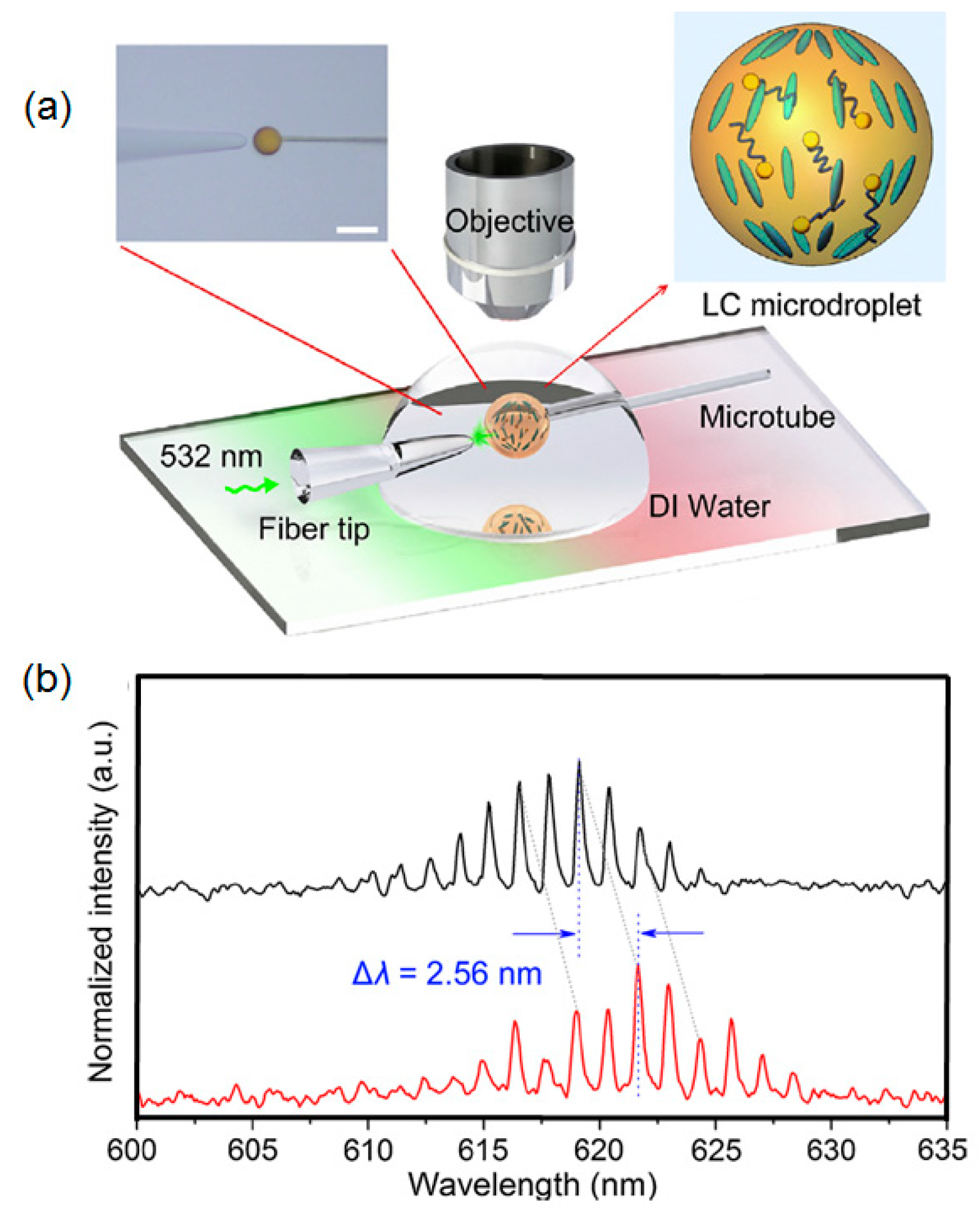
  175. Wang, Y.; Li, H.; Zhao, L.; Liu, Y.; Liu, S.; Yang, J. Tapered optical fiber waveguide coupling to whispering gallery modes of liquid crystal microdroplet for thermal sensing application. Opt. Express 2017, 25, 918. [Google Scholar] [CrossRef] [PubMed]
  176. Duan, R.; Li, Y.; Li, H.; Yang, J. Detection of heavy metal ions using whispering gallery mode lasing in functionalized liquid crystal microdroplets. Biomed. Opt. Express 2019, 10, 6073–6083. [Google Scholar] [CrossRef] [PubMed]
  177. Duan, R.; Li, Y.; Shi, B.; Li, H.; Yang, J. Real-time, quantitative and sensitive detection of urea by whispering gallery mode lasing in liquid crystal microdroplet. Talanta 2020, 209, 120513. [Google Scholar] [CrossRef]
  178. Wang, Y.; Zhao, L.; Xu, A.; Wang, L.; Zhang, L.; Liu, S.; Liu, Y.; Li, H. Detecting enzymatic reactions in penicillinase via liquid crystal microdroplet-based pH sensor. Sens. Actuators B Chem. 2018, 258, 1090–1098. [Google Scholar] [CrossRef]
  179. Minn, K.; Birmingham, B.; Zhang, Z. New development of nanoscale spectroscopy using scanning probe microscope. J. Vac. Sci. Technol. A 2020, 38, 030801. [Google Scholar] [CrossRef]
  180. Dombi, P.; Pápa, Z.; Vogelsang, J.; Yalunin, S.V.; Sivis, M.; Herink, G.; Schäfer, S.; Groß, P.; Ropers, C.; Lienau, C. Strong-field nano-optics. Rev. Mod. Phys. 2020, 92, 1–66. [Google Scholar] [CrossRef]
Figure 1. Wing method (WM) set-up scheme. In the centre of the figure, a sketch summarizes all the parts of the set-up. Laser light is coupled to the fibre in order to control the etching, monitored by a microscope coupled to a Charged Coupled Device (CCD) camera and elaborated by a specific home-made software. In panel (b,c), the lateral views are obtained by a NAVITAR lens zoom. Pictures represent the different steps of the “path” followed to fabricate a nanotip starting from an optical fibre. In (a), the vial containing the etching solution, the oil overlayer, and the fibre is shown. The vial is connected to a rotary motor in the bottom part, while the fibre is connected to another rotary motor. In (b), the lateral and bottom views of the fibre during the etching with the source laser on are shown. Panel (c) shows a subsequent phase of the etching process. In this case, the rod is very small, as it can be seen looking at the laser light leakages along the fibre. In (d), the nanotip is formed. In (e), the image taken with a scanning emission microscope (SEM) shows the small apex size of the tip as the final result of the fabrication method. HF, hydrogen fluoride.
Optics 01 00017 g001
Figure 2. Schematic diagram of the optical measurement setup of a pH sensor based on optical fibre micro/nano tip (OFT) for cellular surface sensing. Reprinted with permission from [126].
Optics 01 00017 g002
Figure 3. Single cell telomerase detection by an optical fibre nanobiosensor. (a) Anti-telomerase immobilised at the apex of the OFT; (b) telomerase interaction with its specific antibody after the insertion of the OFT inside the MCF-7 cell; (c,d) out-of-cell detection of the telomerase by means of three consecutive steps: interaction with biotinylated anti-telomerase as secondary antibody, interaction with strepavidin–alkaline phosphatase conjugate, and introduction of 9H-(1,3-Dichloro-9,9-dimethylacridin-2-one-7-yl) (DDAO)-phosphate solution (1) for the final fluorescence measurement of the enzymatic reaction product—DDAO (2). Reprinted with permission from [30].
Optics 01 00017 g003
Figure 4. (a) A part of the experimental set-up showing the fibre optical nanotip, the cuvette, and the GRIN lens; (b) recorded molecular beacon (MB) fluorescence spectrum after its hybridisation with the 10,000 nM target; (c) increase of the MB fluorescence in the presence of increasing concentrations of the specific target sequence. A negligible signal is observed after the interaction with the random sequence (in yellow).
Optics 01 00017 g004
Figure 5. Working principle of a scanning near-field optical microscopy (SNOM) system with spatial resolution (Δx) for far-field optical microscope (on the left), Synge’s theoretical proposal (in the centre), and near-field scanning optical microscopy (on the right). Numerical aperture (NA) represents the numerical aperture of the microscope objective; d is the dimension of the aperture in the Synge’s proposal. Reproduced from [137] under Creative Commons Attribution License.
Optics 01 00017 g005
Figure 6. (a) The case of an aperture tip. The evanescent field created by a nanoscale opening at the tip apex is scattered from the surface. This scattered light is detected in the far-field. (b) The case of apertureless tip: the near-field light emitted from the surface owing to an external illumination is scattered off of the sharp tip into the far-field to be detected. d represents the distance between the tip and the sample surface [51].
Optics 01 00017 g006
Figure 7. (a) A scheme of the atomic force microscopy (AFM)/SNOM system based on tuning fork and bent optical fibre nanotip in the case of the non-resonant condition. In the inset, the related configuration generally adopted in the case of the double-resonant condition is reported. Reproduced from [64] under Creative Commons Attribution License. (b) The optical beam detection (OBD) system used to detect deflection of the bent nanotip. The laser spot focalised on the fibre tip is clearly visible. The inset reports the SEM image of a so-adopted double bent fibre nanotip. The tip apex is smaller than 50 nm.
Optics 01 00017 g007
Figure 8. (a) A sketch of the improved measurement set-up with the SNOM system, based on the shear-force mechanism and fibre nanotip, for the topographical mapping of whispering gallery modes (WGMs) and the recording of their spectra by means of a multimode fibre. The inset shows the details of the coupling configuration; (b) the recorded spectrum of the WGMs for m ≤ l; (c) a particular of the topographical (on the left) and spatial (on the right) spectral mode map for the fundamental WGM. Reprinted with permission from [80,81]. PMT, photomultiplier; PD, photodiode.
Optics 01 00017 g008
Figure 9. Schematic of the three-port system adopted for coupling the signal and the pump in an active WGM microsphere, where u(t) is the amplitude of the WGM, τ0 is the intrinsic cavity photon lifetime, while τe is the coupling photon lifetime. Reproduced from [171] under Creative Commons Attribution License.
Optics 01 00017 g009
Figure 10. (a) Schematic diagram of the lasing experimental set-up. The 4′-pentyl-biphenyl-4-carboxylic acid (PBA)-doped 4-cyano-4′-pentylbiphenyl (5CB) microdroplet was pumped by a pulsed laser at the wavelength of 532 nm. A tapered tip was used to transmit the excitation beam to the microdroplet (top left inset). A drop of deionized (DI) water was deposited onto a glass slide to serve as the host medium of the microdroplet. The pump light reflection was removed with a 532 nm filter and the emission of the liquid crystal (LC) microdroplet was split with a beam splitter to a spectrometer and CCD camera (not reported in the sketch). Close-up structural diagram of PBA-doped 5CB microdroplet (top right inset). (b) By changing the pH of the surrounding environment, the liquid crystals inside the microdroplet modified their orientation from radial (on the top) to bipolar (on the bottom). A spectral red-shift of the WGM spectra was observed in response of the pH variation. Reprinted with permission from [178].
Optics 01 00017 g010
Table 1. Advantages and disadvantages of the different fabrication techniques used for fibre tip construction.
Fabrication TechniqueAdvantagesDisadvantagesRef.
Grinding and PolishingLow costMechanical instability[9]
Environmental sensitivity
Low reproducibility
Low accuracy
Simple instrumentationLow control of the surface roughness
Thermal PullingLow costNo conical shape in the final tip[82]
Low reproducibility
Low accuracy
Smooth surface roughnessPoor control of surface roughness
Chemical EtchingLow costMechanical instability[55,83,84,85,86,87,88,89,90,91,92,93,94]
Environmental sensitivity
Low reproducibility
Low accuracy
Possible online monitoringLow control of surface roughness
Smooth surface roughness
Simple instrumentation
Focused Ion Beam (FIB) milling High reproducibilityHigh cost[11,95,96,97,98,99,100,101,102]
Time consuming
Possible online monitoringComplex instrumentation
Femtosecond laser machiningHigh resolutionLimited use[9,103,104,105]
High cost
Complex instrumentation
LithographyHigh resolutionHigh cost[9]
Complex instrumentation
Photopolymerisation methodsLow costComplex processing [11,63,106,107,108,109,110,111,112,113,114]
Table 2. Overview of the main scanning near-field optical microscopy (SNOM) feedback mechanisms and their characteristics. SFM, shear-force mechanism; AFM, atomic force microscopy.
Operating Mode (Sketch)Feedback TypeTips AdoptedAdvantagesDisadvantages
SFM/SNOMTuning fork/Shear forceTapered optical fibre/aperture tipsNo limits to sample typesComplex operating mode
Optics 01 00017 i001Easy fabrication methods for tips
Versatility and adaptabilityPoor lateral resolution
AFM/SNOMOptical cantilever/Tapping modeMetal/metal coated cantilever tips aperture tipsNo limits to sample types Easy operating modePossibility to damage the metallic tip
Optics 01 00017 i002Stray light from the cantilever (spectral interferences on the measurement)
STM/SNOMTunneling currentSharp metal tips/apertureless apexHigh spatial resolution and control precision Working in non-contact mode (gap mode)
Mature fabrication methods for tips
Limitation on the sample type (only conducting) operating mode only in reflection applicable only to samples with limited surface ripple
Optics 01 00017 i003

