Electrodeposition Fabrication of Chalcogenide Thin Films for Photovoltaic Applications

 , and
, and
Abstract
:1. Introduction
2. Fundamentals of Electrodeposition
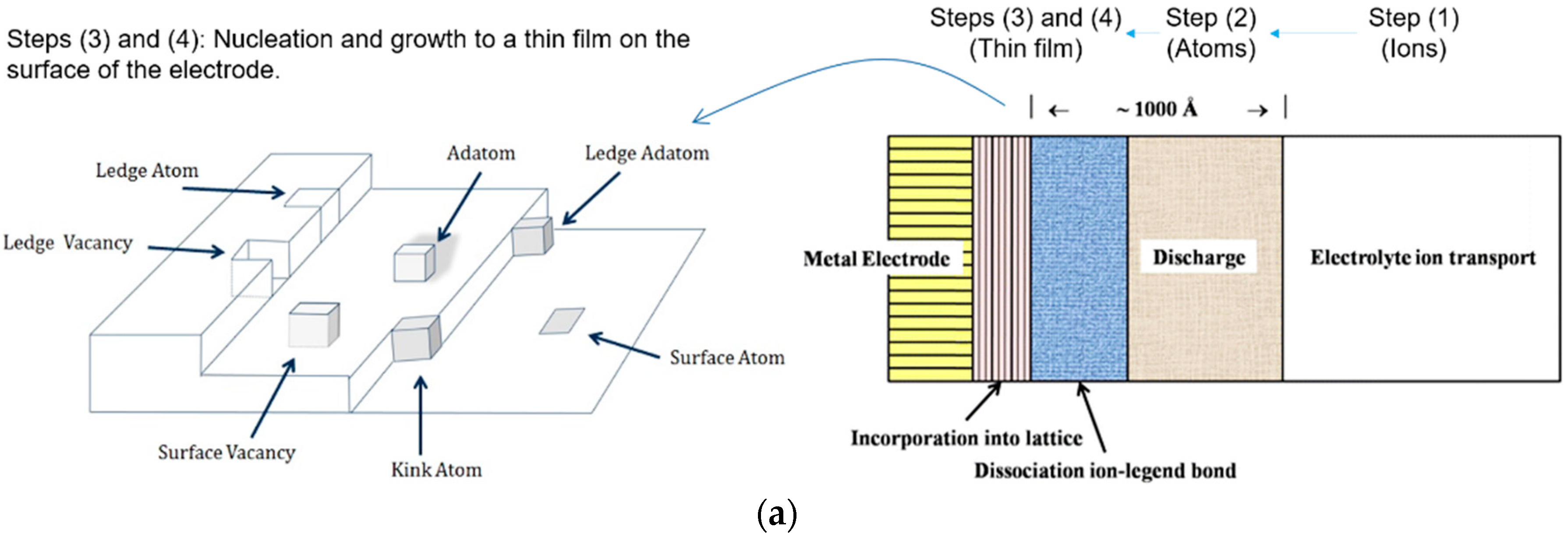
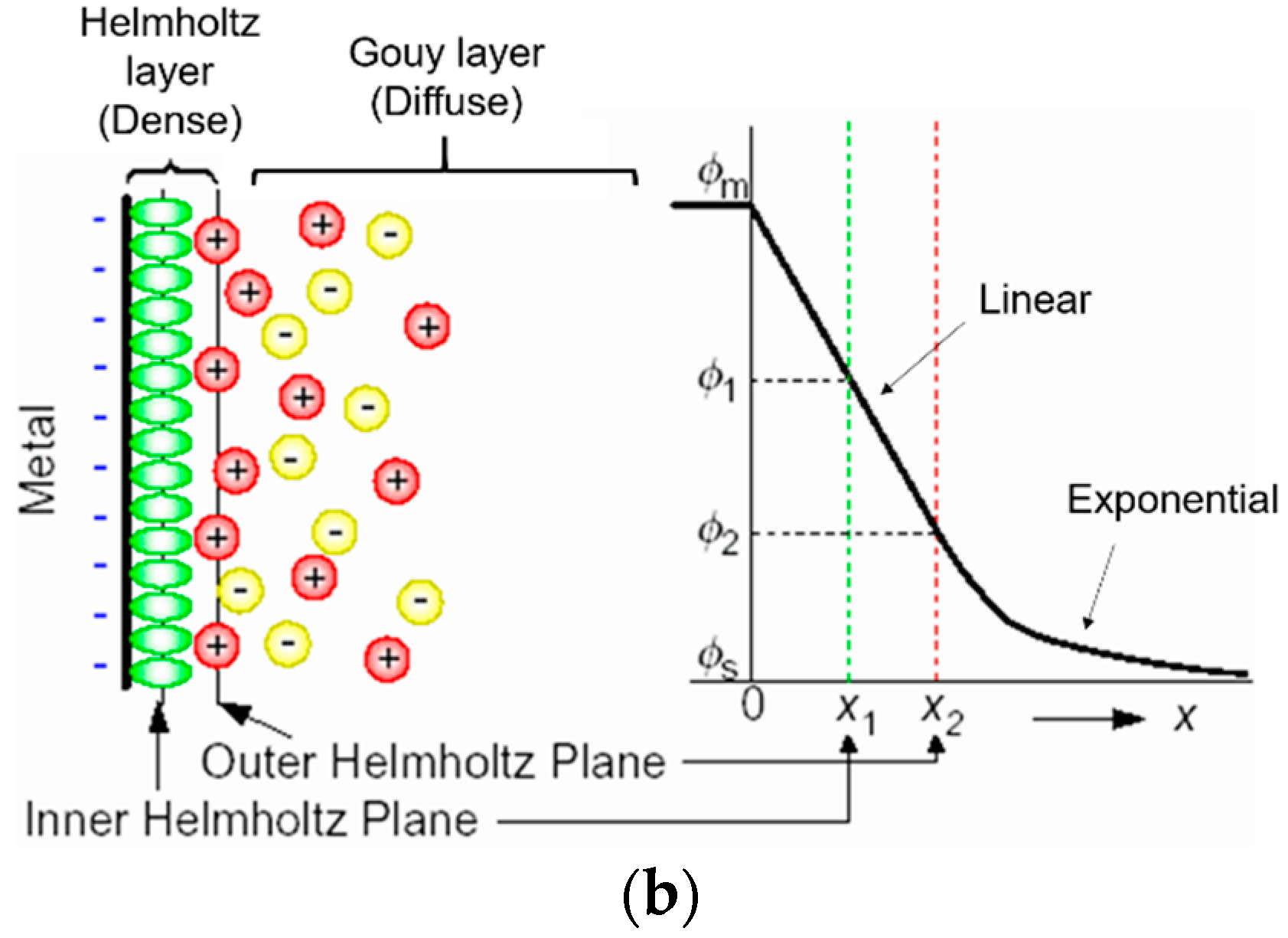
2.1. Mechanism
- The recipe, concentration and viscosity of the electrolyte,
- The chemical environment of the electrolyte (e.g., the pH value),
- Complexing agent added in the electrolyte,
- Temperature during the deposition,
- The voltage and current applied to the deposition bath and,
- The condition of the substrate (at the cathode; e.g., the conductivity and surface roughness), which can affect the mass transfer of cations and the kinetics of the reaction at the cathode surface, either individually or jointly [31].
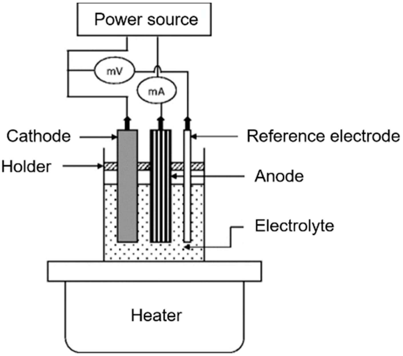
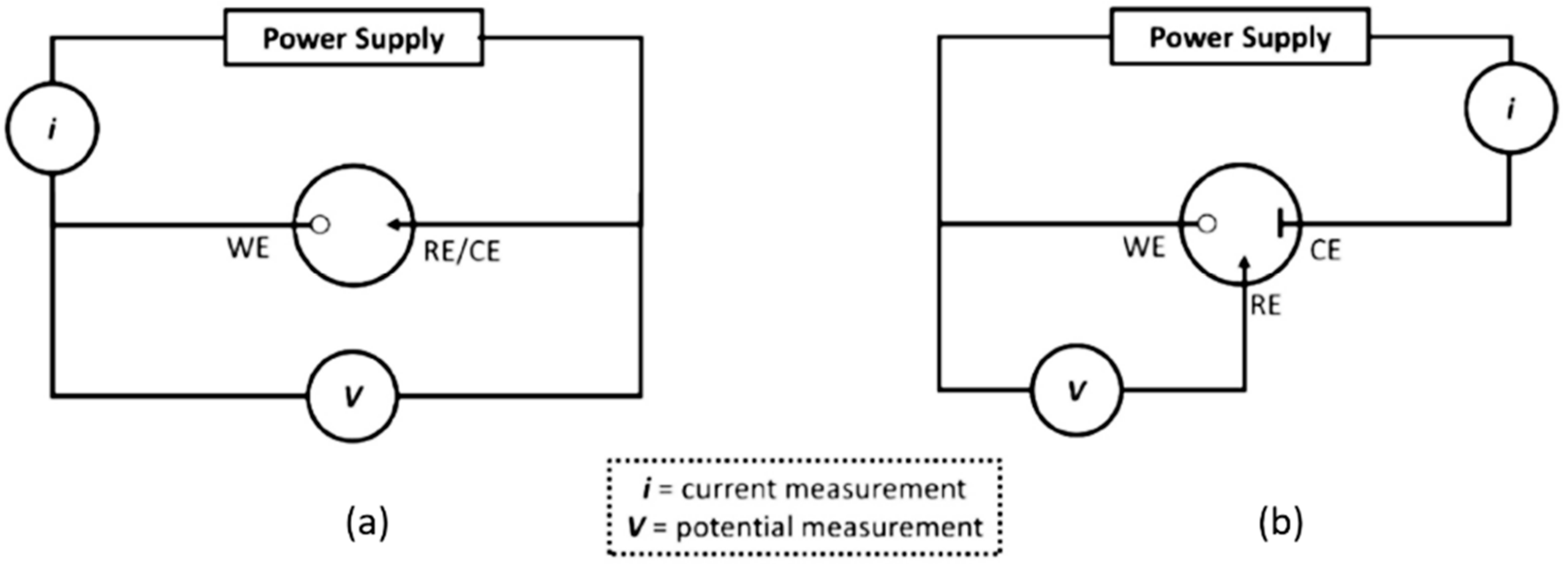
2.2. Two-Electrode and Three-Electrode Configurations
2.3. Potentiostatic and Galvanostatic Modes
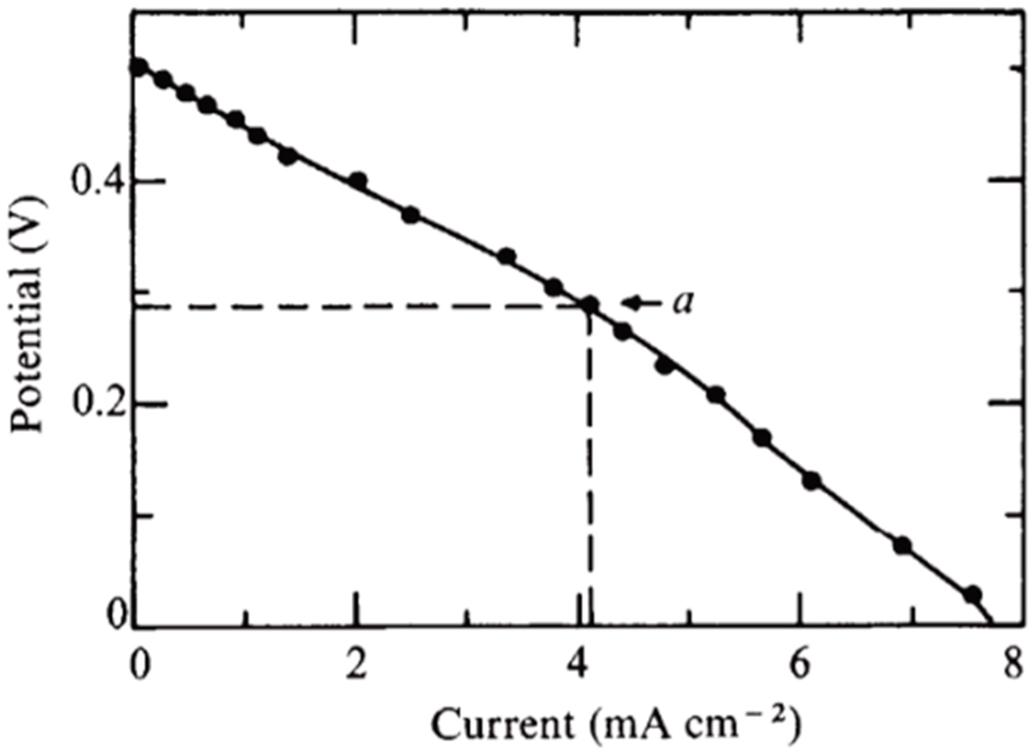
2.4. The Deposition Potential
3. Electrodeposition of Chalcogenide Films
3.1. Cadmium Chalcogenides
3.1.1. CdS
3.1.2. CdSe
3.1.3. CdTe
3.2. Zinc Chalcogenides
3.2.1. ZnS
3.2.2. ZnSe
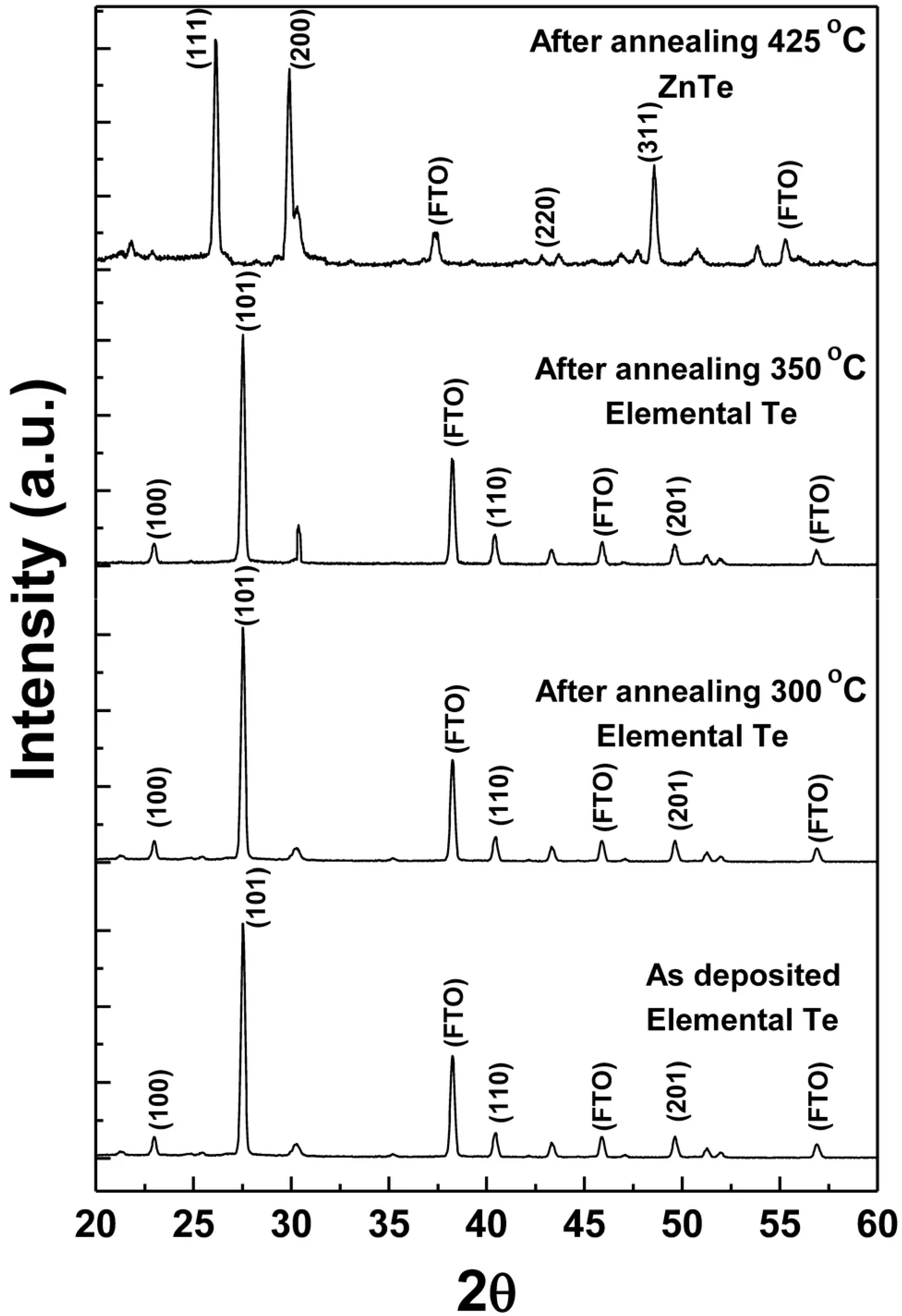
3.2.3. ZnTe
3.3. Copper Chalcogenides
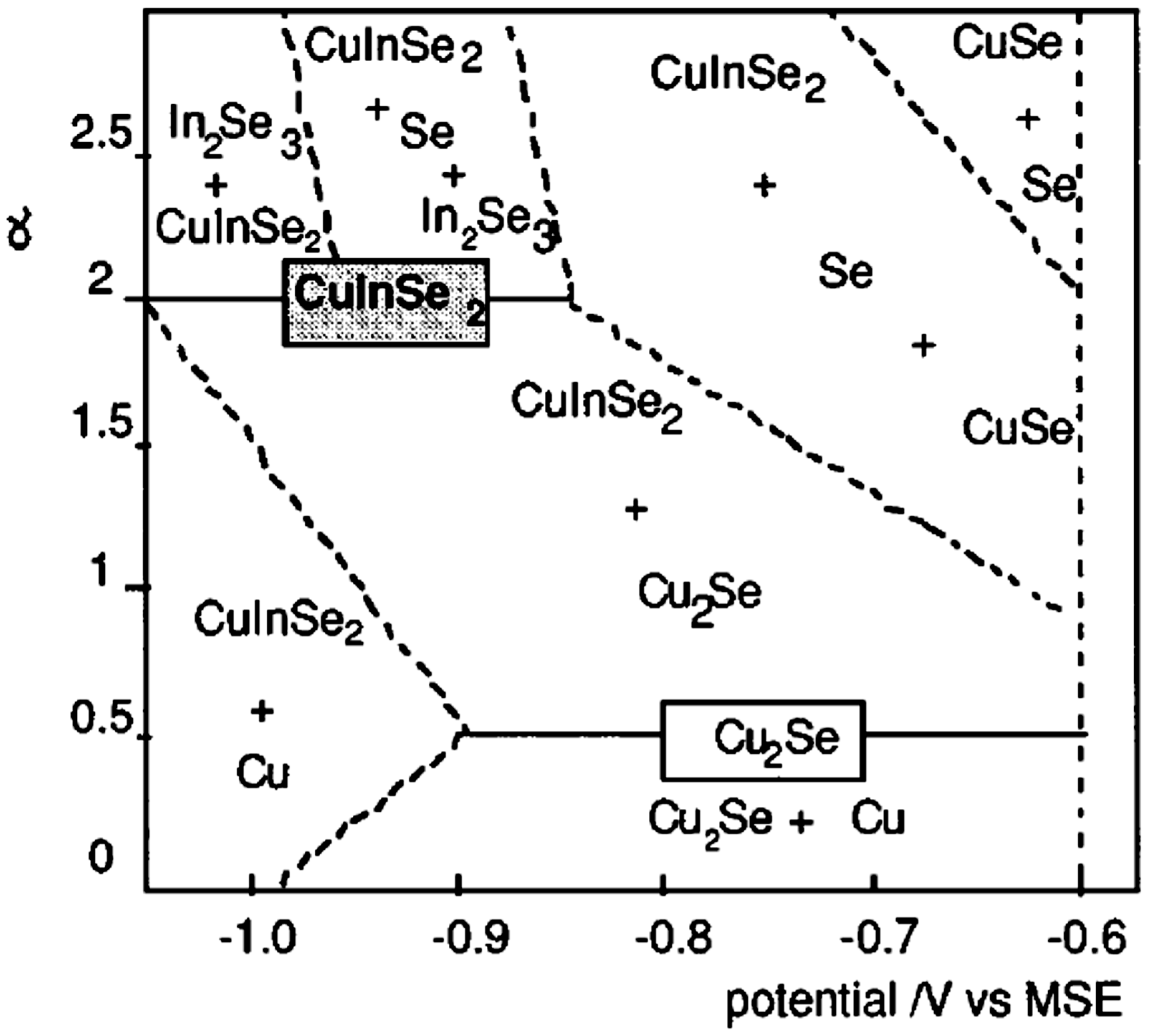
3.3.1. Copper Selenides
3.3.2. Copper Tellurides
3.3.3. Copper Indium Selenides (CIS)
3.3.4. Copper Indium Tellurides (CIT)
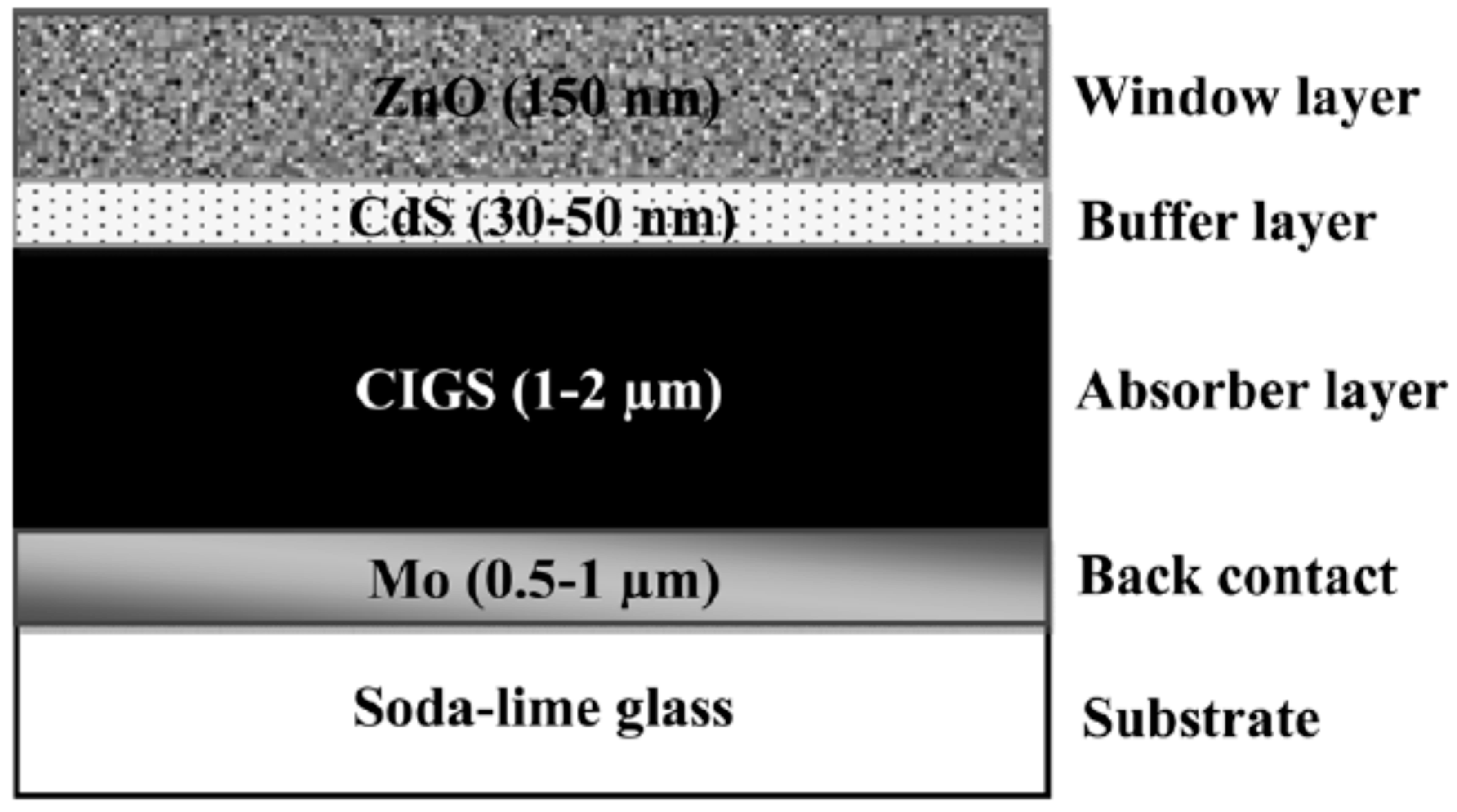
3.3.5. CIGS
- (1)
- One-Step Co-Deposition Method
- (2)
- Two-Stage Selenization Method
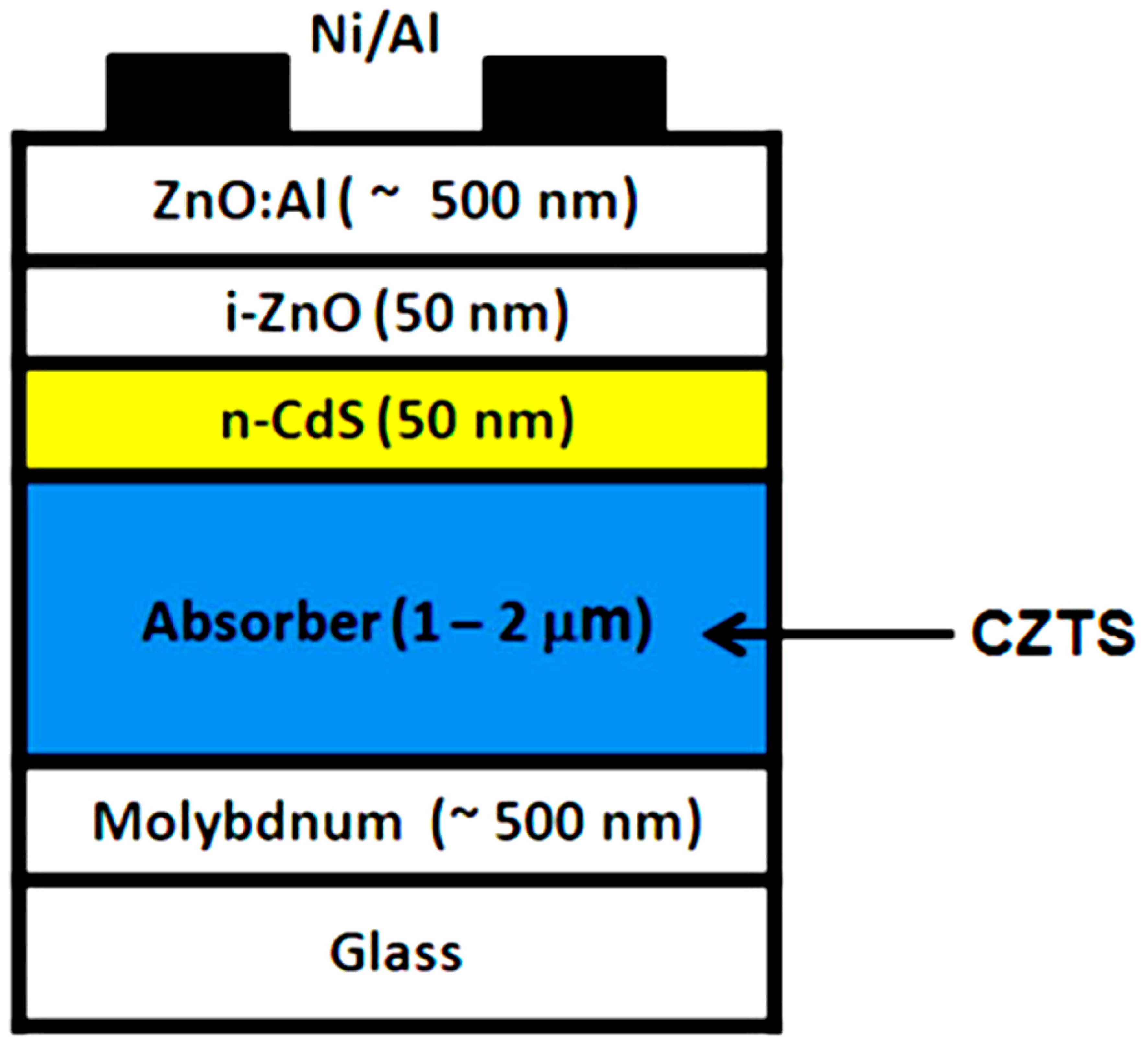
3.3.6. CZTS
- (1)
- One-Step Co-Deposition Method
- (2)
- Two-Stage Sulfurization Method
4. Concluding Remarks
- (1)
- The deposition potential must be selected carefully. The deposition potential is primarily determined by the standard electrode potential of cations and the recipe of the electrolyte that matters the concentration of the cations and the pH value of the electrolyte, but is also affected by some other factors such as the deposition temperature and the type of substrate (for example, FTO glass, ITO glass, stainless steel, copper or carbon). Cyclic voltammetry (CV) is the most effective way to help determine the deposition potential or understand the deposition mechanism.
- (2)
- It is always a challenge to balance the potential adopted for the deposition and the composition of the electrolyte (including the type of the complexing agent use in the electrolyte) in order to achieve the stoichiometric composition, especially in the case of ternary and quaternary chalcogenides. It seems that the stacked layer structure method is relatively advantageous in controlling the composition of the deposited films, in particular when the films consist of multiple elements and the deposition potentials of them are distributed in a wide range. However, since this method involves a sulfurization or selenization treatment of the precursor film comprised of metals, it is not ideal for the fabrication of thick films (>1 μm). In addition, the treatment is usually conducted at high temperatures, making the method not a good fit for most of the flexible substrates.
- (3)
- Complexing agents may have an important impact on the morphology and quality (e.g., the crystallinity and defects) of the deposited film by affecting the concentration of free cations in the electrolyte and thus affecting the deposition rate.
- (4)
- Post heat treatment is usually a necessary step to improve the crystallinity of the deposited films. Not only improving the crystallinity, depending on the atmosphere, post heat treatment can also function to adjust the composition of the films. Post heat treatment else contributes to growing the crystallites and enhancing the contact or adhesion between the deposited film and the substrate.
- (5)
- The use of ionic liquid- and organic solvent-based electrolytes may allow the deposition to be conducted at significantly higher temperatures, which is good for the formation of films with high quality and better crystallinity. However, compared with the aqueous electrolytes, the ionic liquid- and organic solvent-based electrolytes are usually less effective in dissolving inorganic salts. This limits the flexibility of choosing ideal reagents as the sources of elements for the film deposition.
- (6)
- Combining the electrodeposition with other techniques is a feasible way to make the deposited films gain improved quality. For example, the use of pulse potentials for the electrodeposition (known as pulsed electrodeposition) can result in better control of the composition and yield compact films [168]. Integrating electrophoretic [169] or chemical bath deposition [170] into the electrodeposition process may provide more flexibility in adjusting the film composition and, likely, may else lead to films with a more uniform morphology. Adding mechanical perturbations to the working electrode during the electrodeposition has also reported the capability in improving the film’s morphology [171].
5. Perspective
- (1)
- Developing more advanced electrolytes or new techniques to better control the composition of the deposited films, including eliminating the impurity and reducing the secondary phases in the films.
- (2)
- Exploring feasible methods to enhance the density of the deposited films and reduce the defects in the films. The relatively low density of the electrodeposited films and the existence of quite a large number of defects (e.g., the point defects and the planar defects at the grain boundaries) seem to be some of the major reasons that cause the solar cells constructed with the electrodeposited films generally less efficient than the cells that employ the films produced with a vacuum deposition method.
- (3)
- With regard to the ternary and quaternary chalcogenides, especially CIGS and CZTS, it is worth further developing the one-step co-deposition method, with the consideration of achieving selenization or sulfurization during the electrodeposition and thus simplifying the manufacturing operations to make the electrodeposition a more competitive technique in delivering low cost solar cells.
- (4)
- New ideas, for example, nanoparticle-based electrodeposition [172], photo-assisted electrodeposition [173], in situ monitoring of the deposition [174,175], may create the chances to gain better understanding of the kinetics of electrodeposition, make the control of the composition and microstructure of electrodeposited films more effective, and consequently deliver high quality films.
- (5)
- There is generally a lack of theoretical models to simulate the electrodeposition, in particular for the co-deposition of multiple elements. Machine learning is an emerging technology that may potentially be a great tool to predict the synthesis–composition–structure–property relationships of materials [176,177], including the films produced via electrodeposition.
Author Contributions
Funding
Acknowledgments
Conflicts of Interest
References
- Scheer, R.; Schock, H.-W. Chapter 4: Thin Film Material Properties. In Chalcogenide Photovoltaics: Physics, Technologies, and Thin Film Devices; John Wiley & Sons: Hoboken, NJ, USA, 2011; pp. 175–234. [Google Scholar]
- Fu, H. Environmentally friendly and earth-abundant colloidal chalcogenide nanocrystals for photovoltaic applications. J. Mater. Chem. C 2018, 6, 414–445. [Google Scholar] [CrossRef]
- Delbos, S. Kësterite thin films for photovoltaics: A review. EPJ Photovolt. 2012, 3, 35004. [Google Scholar] [CrossRef]
- Qurashi, A. Chapter 11: Solar Cell Application of Metal Chalcogenide Semiconductor Nanostructures. In Metal Chalcogenide Nanostructures for Renewable Energy Applications; John Wiley & Sons: Hoboken, NJ, USA, 2014; pp. 247–267. [Google Scholar]
- Lewis, D.J.; Kevin, P.; Bakr, O.; Muryn, C.A.; Malik, M.A.; O’Brien, P. Routes to tin chalcogenide materials as thin films or nanoparticles: A potentially important class of semiconductor for sustainable solar energy conversion. Inorg. Chem. Front. 2014, 1, 577–598. [Google Scholar] [CrossRef] [Green Version]
- Lee, T.D.; Ebong, A.U. A review of thin film solar cell technologies and challenges. Renew. Sustain. Energy Rev. 2017, 70, 1286–1297. [Google Scholar] [CrossRef]
- Powalla, M.; Paetel, S.; Ahlswede, E.; Wuerz, R.; Wessendorf, C.D.; Magorian Friedlmeier, T. Thin-film solar cells exceeding 22% solar cell efficiency: An overview on CdTe-, Cu(In,Ga)Se2-, and perovskite-based materials. Appl. Phys. Rev. 2018, 5, 041602. [Google Scholar] [CrossRef]
- Pal, K.; Singh, P.; Bhaduri, A.; Thapa, K.B. Current challenges and future prospects for a highly efficient (>20%) kesterite CZTS solar cell: A review. Solar Energy Mater. Solar Cells 2019, 196, 138–156. [Google Scholar] [CrossRef]
- Ji, S.; Ye, C. Cu2ZnSnS4 as a new solar cell material: The history and the future. Rev. Adv. Sci. Eng. 2012, 1, 42–58. [Google Scholar] [CrossRef]
- Zhou, H.; Hsu, W.-C.; Duan, H.-S.; Bob, B.; Yang, W.; Song, T.-B.; Hsu, C.-J.; Yang, Y. CZTS nanocrystals: A promising approach for next generation thin film photovoltaics. Energy Environ. Sci. 2013, 6, 2822–2838. [Google Scholar] [CrossRef]
- Shi, J.; Li, Z.; Zhang, D.; Liu, Q.; Sun, Z.; Huang, S. Fabrication of Cu(In,Ga)Se2 thin films by sputtering from a single quaternary chalcogenide target. Prog. Photovolt. Res. Appl. 2011, 19, 160–164. [Google Scholar] [CrossRef]
- Ramasamy, K.; Malik, M.A.; O’Brien, P. The chemical vapor deposition of Cu2ZnSnS4 thin films. Chem. Sci. 2011, 2, 1170–1172. [Google Scholar] [CrossRef]
- Rana, T.R.; Shinde, N.; Kim, J. Novel chemical route for chemical bath deposition of Cu2ZnSnS4 (CZTS) thin films with stacked precursor thin films. Mater. Lett. 2016, 162, 40–43. [Google Scholar] [CrossRef]
- Dona, J.; Herrero, J. Chemical bath deposition of CdS thin films: An approach to the chemical mechanism through study of the film microstructure. J. Electrochem. Soc. 1997, 144, 4081. [Google Scholar] [CrossRef]
- Kale, R.; Sartale, S.; Chougule, B.; Lokhande, C. Growth and characterization of nanocrystalline CdSe thin films deposited by the successive ionic layer adsorption and reaction method. Semicond. Sci. Technol. 2004, 19, 980. [Google Scholar] [CrossRef]
- Mali, S.S.; Patil, B.M.; Betty, C.A.; Bhosale, P.N.; Oh, Y.W.; Jadkar, S.R.; Devan, R.S.; Ma, Y.-R.; Patil, P.S. Novel synthesis of kesterite Cu2ZnSnS4 nanoflakes by successive ionic layer adsorption and reaction technique: Characterization and application. Electrochim. Acta 2012, 66, 216–221. [Google Scholar] [CrossRef]
- Wibowo, R.A.; Jung, W.H.; Kim, K.H. Synthesis of Cu2ZnSnSe4 compound powders by solid state reaction using elemental powders. J. Phys. Chem. Solids 2010, 71, 1702–1706. [Google Scholar] [CrossRef]
- Valdes, M.; Modibedi, M.; Mathe, M.; Hillie, T.; Vazquez, M. Electrodeposited Cu2ZnSnS4 thin films. Electrochim. Acta 2014, 128, 393–399. [Google Scholar] [CrossRef]
- Friedfeld, R.; Raffaelle, R.; Mantovani, J. Electrodeposition of CuInxGa1−xSe2 thin films. Sol. Energy Mater. Sol. Cells 1999, 58, 375–385. [Google Scholar] [CrossRef]
- Deligianni, H.; Ahmed, S.; Romankiw, L.T. The next frontier: Electrodeposition for solar cell fabrication. Electrochem. Soc. Interface 2011, 20, 47. [Google Scholar] [CrossRef]
- Kim, S.Y.; Kim, J. Fabrication of CIGS thin films by using spray pyrolysis and post-selenization. J. Korean Phys. Soc. 2012, 60, 2018–2024. [Google Scholar] [CrossRef]
- Kamoun, N.; Bouzouita, H.; Rezig, B. Fabrication and characterization of Cu2ZnSnS4 thin films deposited by spray pyrolysis technique. Thin Solid Films 2007, 515, 5949–5952. [Google Scholar] [CrossRef]
- Brenner, A. Part III: Introduction to Practical Considerations and Specific Information on the Electrodeposition of Alloys. In Electrodeposition of Alloys: Principles and Practice; Elsevier: Amsterdam, The Netherlands, 2013; pp. 409–678. [Google Scholar]
- Lincot, D. Electrodeposition of semiconductors. Thin Solid Films 2005, 487, 40–48. [Google Scholar] [CrossRef]
- Soare, V.; Burada, M.; Mitrica, D.; Badilita, V.; Stoiciu, F.; Lungu, C.; Ghenescu, V.; Rusu, M.; Antohe, Ş. Electrodeposition and characterization of CuInSe2/CdS multilayered thin films deposited on flexible substrate. Optoelectron. Adv. Mater. Rapid Commun. 2010, 4, 2018–2021. [Google Scholar]
- Mohammadzadeh, A.; Fox-Robichaud, A.; Selvaganapathy, P.R. Electroplating of Multiple Materials in Parallel Using Patterned Gels with Applications in Electrochemical Sensing. Sensors 2020, 20, 886. [Google Scholar] [CrossRef] [PubMed] [Green Version]
- Shaikh, A.V.; Mane, R.S.; Joo, O.-S.; Han, S.-H.; Pathan, H.M. Electrochemical deposition of cadmium selenide films and their properties: A review. J. Solid State Electrochem. 2017, 21, 2517–2530. [Google Scholar] [CrossRef]
- Mallik, A.; Ray, B. Evolution of principle and practice of electrodeposited thin film: A review on effect of temperature and sonication. Int. J. Electrochem. 2011, 2011, 568023. [Google Scholar] [CrossRef] [Green Version]
- Electric Double Layer. Available online: https://web.nmsu.edu/~snsm/classes/chem435/Lab14/double_layer.html (accessed on 20 August 2020).
- Zangari, G. Electrodeposition of alloys and compounds in the era of microelectronics and energy conversion technology. Coatings 2015, 5, 195–218. [Google Scholar] [CrossRef]
- Pandey, R.K.; Sahu, S.; Chandra, S. Chapter 3: Nucleation and Growth. In Handbook of Semiconductor Electrodeposition; M. Dekker: New York, NY, USA, 1996; pp. 61–88. [Google Scholar]
- Pasa, A.A.; Munford, M.L. Electrodeposition—Encyclopedia of Chemical Processing. Nova 2006, 821–832. [Google Scholar] [CrossRef]
- Raccichini, R.; Amores, M.; Hinds, G. Critical review of the use of reference electrodes in li-ion batteries: A diagnostic perspective. Batteries 2019, 5, 12. [Google Scholar] [CrossRef] [Green Version]
- Tatiparti, S.S.V.; Ebrahimi, F. Potentiostatic versus galvanostatic electrodeposition of nanocrystalline Al–Mg alloy powders. J. Solid State Electrochem. 2012, 16, 1255–1262. [Google Scholar] [CrossRef]
- Lou, H.H.; Huang, Y. Electroplating. Encyclopedia of Chemical Processing; Taylor & Francis: Oxfordshire, UK, 2006; pp. 1–10. [Google Scholar]
- Elgrishi, N.; Rountree, K.J.; McCarthy, B.D.; Rountree, E.S.; Eisenhart, T.T.; Dempsey, J.L. A practical beginner’s guide to cyclic voltammetry. J. Chem. Educ. 2018, 95, 197–206. [Google Scholar] [CrossRef]
- Fathy, M.; Kashyout, A.E.-H.B.; Elyamny, S.; Roston, G.D.; Bishara, A.A. Effect of CdCl2 concentration and heat treatment on electrodeposited nano-crystalline CdS thin films from non-aqueous solution. Int. J. Electrochem. Sci. 2014, 9, 6155–6165. [Google Scholar]
- Altiokka, B.; Yildirim, A.K. Electrodeposition of CdS thin films at various pH values. J. Korean Phys. Soc. 2018, 72, 687–691. [Google Scholar] [CrossRef]
- Lade, S.; Uplane, M.; Lokhande, C. Studies on the electrodeposition of CdS films. Mater. Chem. Phys. 1998, 53, 239–242. [Google Scholar] [CrossRef]
- Echendu, O.K.; Dejene, F.B.; Dharmadasa, I.M.; Eze, F.C. Characteristics of nanocrystallite-CdS produced by low-cost electrochemical technique for thin film photovoltaic application: The influence of deposition voltage. Int. J. Photoenergy 2017, 2017, 3989432. [Google Scholar] [CrossRef]
- Alam, A.; Cranton, W.; Dharmadasa, I. Electrodeposition of CdS thin-films from cadmium acetate and ammonium thiosulphate precursors. J. Mater. Sci. Mater. Electron. 2019, 30, 4580–4589. [Google Scholar] [CrossRef] [Green Version]
- Mammadov, M.; Aliyev, A.S.; Elrouby, M. Electrodeposition of cadmium sulfide. Int. J. Thin Film Sci. Technol. 2012, 1, 43–53. [Google Scholar]
- Baranski, A.S.; Fawcett, W.R.; McDonald, A.C.; de Nobriga, R.M.; MacDonald, J.R. The structural characterization of cadmium sulfide films grown by cathodic electrodeposition. J. Electrochem. Soc. 1981, 128, 963. [Google Scholar] [CrossRef]
- Lade, S.; Lokhande, C. Electrodeposition of CdS from non-aqueous bath. Mater. Chem. Phys. 1997, 49, 160–163. [Google Scholar] [CrossRef]
- Izgorodin, A.; Winther-Jensen, O.; Winther-Jensen, B.; MacFarlane, D.R. CdS thin-film electrodeposition from a phosphonium ionic liquid. Phys. Chem. Chem. Phys. 2009, 11, 8532–8537. [Google Scholar] [CrossRef]
- Hodes, G.; Manassen, J.; Cahen, D. Photoelectrochemical energy conversion and storage using polycrystalline chalcogenide electrodes. Nature 1976, 261, 403–404. [Google Scholar] [CrossRef]
- Kazacos, M.S.; Miller, B. Electrodeposition of CdSe films from selenosulfite solution. J. Electrochem. Soc. 1980, 127, 2378. [Google Scholar] [CrossRef]
- Teh, L.; Furin, V.; Martucci, A.; Guglielmi, M.; Wong, C.; Romanato, F. Electrodeposition of CdSe on nanopatterned pillar arrays for photonic and photovoltaic applications. Thin Solid Films 2007, 515, 5787–5791. [Google Scholar] [CrossRef]
- Sarangi, S.; Sahu, S. CdSe nanocrystalline thin films: Composition, structure and optical properties. Phys. E Low-Dimens. Syst. Nanostruct. 2004, 23, 159–167. [Google Scholar] [CrossRef]
- Szabo, J.P.; Cocivera, M. Mechanism of electrodeposition of cadmium selenide from solution. Can. J. Chem. 1988, 66, 1065–1072. [Google Scholar] [CrossRef]
- Bouroushian, M. Chapter 3: Electrochemical Preparations—Conventional Coatings and Structures. In Electrochemistry of Metal Chalcogenides; Springer Science & Business Media: Berlin/Heidelberg, Germany, 2010; pp. 76–152. [Google Scholar]
- Dale, P.J.; Samantilleke, A.P.; Shivagan, D.D.; Peter, L.M. Synthesis of cadmium and zinc semiconductor compounds from an ionic liquid containing choline chloride and urea. Thin Solid Films 2007, 515, 5751–5754. [Google Scholar] [CrossRef]
- Kariper, I.; Bağlayan, O.; Gode, F. Fabrication and optical characterization of CdSe thin films grown by chemical bath deposition. Acta Phys. Pol. A 2015, 128, B-219–B-221. [Google Scholar] [CrossRef]
- Park, J.H.; Wang, Q.; Zhu, K.; Frank, A.J.; Kim, J.Y. Electrochemical Deposition of Conformal Semiconductor Layers in Nanoporous Oxides for Sensitized Photoelectrodes. ACS Omega 2019, 4, 19772–19776. [Google Scholar] [CrossRef] [Green Version]
- Alkire, R.C.; Kolb, D.M.; Lipkowski, J.; Ross, P.N. Chapter 2: Tailoring of Interfaces for the Photoelectrochemical Conversion of Solar Energy. In Photoelectrochemical Materials and Energy Conversion Processes; John Wiley & Sons: Hoboken, NJ, USA, 2010; Volume 24, pp. 61–181. [Google Scholar]
- Chowdhury, R.; Islam, M.; Sabeth, F.; Mustafa, G.; Farhad, S.; Saha, D.; Chowdhury, F.; Hussain, S.; Islam, A. Characterization of electrodeposited cadmium selenide thin films. Dhaka Univ. J. Sci. 2012, 60, 137–140. [Google Scholar] [CrossRef]
- Pawar, S.; Moholkar, A.; Bhosale, C. Influence of pH on electrochemically deposited CdSe thin films. Mater. Lett. 2007, 61, 1034–1038. [Google Scholar] [CrossRef]
- Rashwan, S.; Abd El-Wahab, S.; Mohamed, M. Electrodeposition and characterization of CdSe semiconductor thin films. J. Mater. Sci. Mater. Electron. 2007, 18, 575–585. [Google Scholar] [CrossRef]
- Baubinas, R.; Januškevičius, Z.; Sakalas, A. CdSe single crystals with n-and p-type of conductivity approaching intrinsic. Mater. Res. Bull. 1973, 8, 817–823. [Google Scholar] [CrossRef]
- Ohtsuka, T.; Kawamata, J.; Zhu, Z.; Yao, T. p-type CdSe grown by molecular beam epitaxy using a nitrogen plasma source. Appl. Phys. Lett. 1994, 65, 466–468. [Google Scholar] [CrossRef]
- Diso, D.; Fauzi, F.; Echendu, O.; Olusola, O.; Dharmadasa, I. Optimisation of CdTe electrodeposition voltage for development of CdS/CdTe solar cells. J. Mater. Sci. Mater. Electron. 2016, 27, 12464–12472. [Google Scholar] [CrossRef]
- Rastogi, A.; Sharma, R. Properties and mechanism of solar absorber CdTe thin film synthesis by unipolar galvanic pulsed electrodeposition. J. Appl. Electrochem. 2009, 39, 167–176. [Google Scholar] [CrossRef]
- Duffy, N.; Peter, L.; Wang, R.; Lane, D.; Rogers, K. Electrodeposition and characterisation of CdTe films for solar cell applications. Electrochim. Acta 2000, 45, 3355–3365. [Google Scholar] [CrossRef]
- Sella, C.; Boncorps, P.; Vedel, J. The electrodeposition mechanism of CdTe from acidic aqueous solutions. J. Electrochem. Soc. 1986, 133, 2043. [Google Scholar] [CrossRef]
- Bhattacharya, R.; Rajeshwar, K. Electrodeposition of CdTe thin films. J. Electrochem. Soc. 1984, 131, 2032. [Google Scholar] [CrossRef]
- Patil, V.; Sutrave, D.; Shahane, G.; Deshmukh, L. Cadmium telluride thin films: Growth from solution and characteristics. Thin Solid Films 2001, 401, 35–38. [Google Scholar] [CrossRef]
- Dharmadasa, I.; Bingham, P.A.; Echendu, O.; Salim, H.; Druffel, T.; Dharmadasa, R.; Sumanasekera, G.; Dharmasena, R.; Dergacheva, M.; Mit, K. Fabrication of CdS/CdTe-based thin film solar cells using an electrochemical technique. Coatings 2014, 4, 380–415. [Google Scholar] [CrossRef]
- Diso, D.G. Research and Development of CdTe Based Thin Film PV Solar Cells. Ph.D. Thesis, Sheffield Hallam University, Sheffield, UK, 2011. [Google Scholar]
- Takahashi, M.; Uosaki, K.; Kita, H.; Yamaguchi, S. Resistivity, carrier concentration, and carrier mobility of electrochemically deposited CdTe films. J. Appl. Phys. 1986, 60, 2046–2049. [Google Scholar] [CrossRef] [Green Version]
- Echendu, O.; Okeoma, K.; Oriaku, C.; Dharmadasa, I. Electrochemical deposition of CdTe semiconductor thin films for solar cell application using two-electrode and three-electrode configurations: A comparative study. Adv. Mater. Sci. Eng. 2016, 2016, 3581725. [Google Scholar] [CrossRef] [Green Version]
- Duffy, N.; Peter, L.; Wang, R. Characterisation of CdS∣ CdTe heterojunctions by photocurrent spectroscopy and electrolyte electroreflectance/absorbance spectroscopy (EEA/EER). J. Electroanal. Chem. 2002, 532, 207–214. [Google Scholar] [CrossRef]
- Bonilla, S.; Dalchiele, E.A. Electrochemical deposition and characterization of CdTe polycrystalline thin films. Thin Solid Films 1991, 204, 397–403. [Google Scholar] [CrossRef]
- Asabe, M.; Ubale, V.; Manikshete, A.; Vader, V.; Rajmane, S.; Delekar, S. Properties of electrochemically deposited CdTe thin films: Annealing effect. J. Mater. Sci. Mater. Electron. 2013, 24, 4655–4661. [Google Scholar] [CrossRef]
- Shenouda, A.Y.; El Sayed, M. Electrodeposition, characterization and photo electrochemical properties of CdSe and CdTe. Ain Shams Eng. J. 2015, 6, 341–346. [Google Scholar] [CrossRef] [Green Version]
- Echendu, O.; Dejene, B.; Hone, F. Comparative performance of CdS/CdTe thin film solar cells fabricated with electrochemically deposited CdTe from 2-electrode and 3-electrode set-ups. Mater. Sci. Eng. B 2018, 232, 55–60. [Google Scholar] [CrossRef]
- Ray, A. Electrodeposition of thin films for low-cost solar cells. In Electroplat. of Nanostructures; InTech: Rijeka, Croatia, 2015. [Google Scholar]
- Major, J.; Treharne, R.; Phillips, L.; Durose, K. A low-cost non-toxic post-growth activation step for CdTe solar cells. Nature 2014, 511, 334–337. [Google Scholar] [CrossRef]
- Zhang, W.; Liu, J.; Guo, Z.; Yao, S.; Wang, H. Synthesis and characterization of CdTe nanoparticle-sensitized TiO 2 nanotube arrays for photocatalysis. J. Mater. Sci. Mater. Electron. 2017, 28, 9505–9513. [Google Scholar] [CrossRef]
- Zhang, Y.; Wu, W.; Liu, Y.; Yang, W.; Chen, W.; Zhao, J. Alkaline electrolyte: Toward high-quality CdTe films with the assistance of strong complexing agent and organic base. CrystEngComm 2018, 20, 8–11. [Google Scholar] [CrossRef]
- Cho, D.H.; Lee, W.J.; Wi, J.H.; Han, W.S.; Kim, T.G.; Kim, J.W.; Chung, Y.D. Interface analysis of Cu(In,Ga)Se2 and ZnS formed using sulfur thermal cracker. ETRI J. 2016, 38, 265–271. [Google Scholar] [CrossRef] [Green Version]
- Lukianova, O.; Klochko, N.; Khrypunov, G.; Kopach, V.; Lyubov, V. Development of n-ZnS/p-Cu2ZnSnS4 heterojunction for thin film solar cells. In Proceedings of the 2016 International Conference on Nanomaterials: Application & Properties (NAP), Lviv, Ukraine, 14–19 September 2016; pp. 02NEA05-01–02NEA05-03. [Google Scholar]
- Mkawi, E.; Ibrahim, K.; Ali, M.; Farrukh, M.; Mohamed, A. Electrodeposited ZnS precursor layer with improved electrooptical properties for efficient Cu2ZnSnS4 thin-film solar cells. J. Electron. Mater. 2015, 44, 3380–3387. [Google Scholar] [CrossRef]
- Lokhande, C.; Jadhav, M.; Pawar, S. Electrodeposition of ZnS films from an alkaline bath. J. Electrochem. Soc. 1989, 136, 2756–2757. [Google Scholar] [CrossRef]
- Zhu, H.; Huang, J.; Wang, Y.; Cao, L.; He, H.; Wu, J. Synthesis and characterisation of ZnS optical thin films through cathodic electrodeposition technique. Surf. Eng. 2011, 27, 42–45. [Google Scholar] [CrossRef]
- Matsuda, N.; Okamoto, N.; Saito, T. Electrodeposition of ZnS and evaluation of its optical property. In Proceedings of the 2018 International Conference on Electronics Packaging and iMAPS All Asia Conference (ICEP-IAAC), Kuwana, Japan, 17–21 April 2018; pp. 566–569. [Google Scholar]
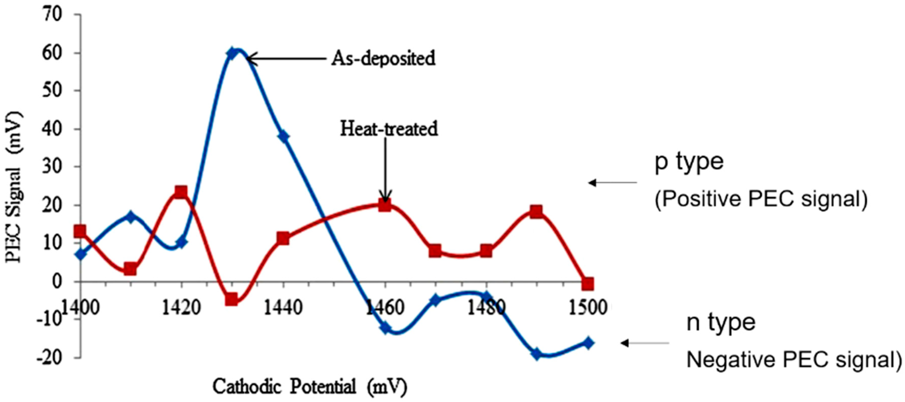
- Madugu, M.L.; Olusola, O.I.-O.; Echendu, O.K.; Kadem, B.; Dharmadasa, I.M. Intrinsic doping in electrodeposited ZnS thin films for application in large-area optoelectronic devices. J. Electron. Mater. 2016, 45, 2710–2717. [Google Scholar] [CrossRef]
- Zakerian, F.; Kafashan, H. Investigation the effect of annealing parameters on the physical properties of electrodeposited ZnS thin films. Superlattices Microstruct. 2018, 124, 92–106. [Google Scholar] [CrossRef]
- Hassane, B.; Benmoussa, D. Investigation of Absorber Layer Thickness Effect on CIGS Solar Cell in Different Cases of Buffer Layers. J. Nano Electron. Phys. 2018, 10, 1–2. [Google Scholar] [CrossRef]
- Ohtake, Y.; Kushiya, K.; Ichikawa, M.; Yamada, A.; Konagai, M. Polycrystalline Cu(InGa)Se2 thin-film solar cells with ZnSe buffer layers. Jpn. J. Appl. Phys. 1995, 34, 5949. [Google Scholar] [CrossRef]
- Konagai, M.; Ohtake, Y.; Okamoto, T. Development of Cu(InGa)Se2 Thin Film Solar Cells with Cd-Free Buffer Layers. MRS Online Proc. Libr. Arch. 1996, 426, 153. [Google Scholar] [CrossRef]
- Chandramohan, R.; Sanjeeviraja, C.; Mahalingam, T. Preparation of zinc selenide thin films by electrodeposition technique for solar cell applications. Phys. Status Solidi A Appl. Res. 1997, 163, R11–R12. [Google Scholar] [CrossRef]
- Kathalingam, A.; Mahalingam, T.; Sanjeeviraja, C. Optical and structural study of electrodeposited zinc selenide thin films. Mater. Chem. Phys. 2007, 106, 215–221. [Google Scholar] [CrossRef]
- Natarajan, C.; Sharon, M.; Levy-Clement, C.; Neumann-Spallart, M. Electrodeposition of zinc selenide. Thin Solid Films 1994, 237, 118–123. [Google Scholar] [CrossRef]
- Kowalik, R.; Żabiński, P.; Fitzner, K. Electrodeposition of ZnSe. Electrochim. Acta 2008, 53, 6184–6190. [Google Scholar] [CrossRef]
- Rusu, G.; Diciu, M.; Pirghie, C.; Popa, E. Structural characterization and optical properties of ZnSe thin films. Appl. Surf. Sci. 2007, 253, 9500–9505. [Google Scholar] [CrossRef]
- Laks, D.; Van de Walle, C.; Neumark, G.; Blöchl, P.; Pantelides, S. Native defects and self-compensation in ZnSe. Phys. Rev. B 1992, 45, 10965. [Google Scholar] [CrossRef] [PubMed] [Green Version]
- Manzoli, A.; Eguiluz, K.; Salazar-Banda, G.; Machado, S. Electrodeposition and characterization of undoped and nitrogen-doped ZnSe films. Mater. Chem. Phys. 2010, 121, 58–62. [Google Scholar] [CrossRef]
- Gromboni, M.F.; Mascaro, L.H. Optical and structural study of electrodeposited zinc selenide thin films. J. Electroanal. Chem. 2016, 780, 360–366. [Google Scholar] [CrossRef]
- Samantilleke, A.; Boyle, M.; Young, J.; Dharmadasa, I. Electrodeposition of n-type and p-type ZnSe thin films for applications in large area optoelectronic devices. J. Mater. Sci. Mater. Electron. 1998, 9, 289–290. [Google Scholar] [CrossRef]
- Jun, Y.; Kim, K.-J.; Kim, D. Electrochemical synthesis of Cu-doped ZnTe films as back contacts to CdTe solar cells. Met. Mater. 1999, 5, 279–285. [Google Scholar] [CrossRef]
- Tang, J.; Mao, D.; Feng, L.; Song, W.; Trefny, J. The properties and optimization of ZnTe: Cu back contacts on CdTe/CdS thin film solar cells. In Proceedings of the Conference Record of the Twenty Fifth IEEE Photovoltaic Specialists Conference-1996, Washington, DC, USA, 13–17 May 1996; pp. 925–928. [Google Scholar]
- Mondal, A.; McCandless, B.E.; Birkmire, R.W. Electrochemical deposition of thin ZnTe films as a contact for CdTe solar cells. Sol. Energy Mater. Sol. Cells 1992, 26, 181–187. [Google Scholar] [CrossRef]
- Mahalingam, T.; John, V.; Rajendran, S.; Sebastian, P. Electrochemical deposition of ZnTe thin films. Semicond. Sci. Technol. 2002, 17, 465. [Google Scholar] [CrossRef]
- Skhouni, O.; El Manouni, A.; Mollar, M.; Schrebler, R.; Marí, B. ZnTe thin films grown by electrodeposition technique on Fluorine Tin Oxide substrates. Thin Solid Films 2014, 564, 195–200. [Google Scholar] [CrossRef]
- Bouroushian, M.; Kosanovic, T.; Karoussos, D.; Spyrellis, N. Electrodeposition of polycrystalline ZnTe from simple and citrate-complexed acidic aqueous solutions. Electrochim. Acta 2009, 54, 2522–2528. [Google Scholar] [CrossRef]
- Hossain, M.; Siddiquee, K.; Islam, O.; Gafur, M.; Qadir, M.; Ahmed, N. Characterization of electrodeposited ZnTe thin films. J. Opt. 2019, 48, 295–301. [Google Scholar] [CrossRef]
- Catrangiu, A.; Beregoi, M.; Cojocaru, A.; Anicai, L.; Cotarta, A.; Visan, T. Electrochemical Deposition of Zinc Telluride Thin Films from Ethaline Ionic Liquid. Chalcogenide Lett. 2016, 13, 187–199. [Google Scholar]
- Coughlan, C.; Ibanez, M.; Dobrozhan, O.; Singh, A.; Cabot, A.; Ryan, K.M. Compound copper chalcogenide nanocrystals. Chem. Rev. 2017, 117, 5865–6109. [Google Scholar] [CrossRef]
- Lippkow, D.; Strehblow, H.-H. Structural investigations of thin films of copper–selenide electrodeposited at elevated temperatures. Electrochim. Acta 1998, 43, 2131–2140. [Google Scholar] [CrossRef]
- Dergacheva, M.; Chaikin, V.; Grigor’eva, V.; Pantileeva, E. Electrodeposition of CuSex compounds onto carbon-containing electrodes. Russ. J. Appl. Chem. 2004, 77, 1273–1278. [Google Scholar] [CrossRef]
- Grozdanov, I. Electroconductive copper selenide films on transparent polyester sheets. Synth. Met. 1994, 63, 213–216. [Google Scholar] [CrossRef]
- He, W.; Zhang, H.; Zhang, Y.; Liu, M.; Zhang, X.; Yang, F. Electrodeposition and characterization of CuTe and Cu2Te thin films. J. Nanomater. 2015, 2015, 240525. [Google Scholar] [CrossRef] [Green Version]
- Jeyakumar, P.; Thanikaikarasan, S.; Natarajan, B. Role of substrate in electrodeposited copper telluride thin films. J. Mater. Sci. Mater. Electron. 2017, 28, 2538–2544. [Google Scholar] [CrossRef]
- Ghosh, A.; Mitra, M.; Banerjee, D.; Mondal, A. Facile electrochemical deposition of Cu7Te4 thin films with visible-light driven photocatalytic activity and thermoelectric performance. RSC Adv. 2016, 6, 22803–22811. [Google Scholar] [CrossRef]
- Uda, H.; Ikegami, S.; Sonomura, H. Annealing effect of Cu2TeAu contact to evaporated CdTe film on photovoltaic properties of CdS/CdTe solar cell. Sol. Energy Mater. Sol. Cells 1998, 50, 141–146. [Google Scholar] [CrossRef]
- Kim, S.; Jeon, J.; Suh, J.; Hong, J.; Kim, T.; Kim, K.; Cho, S. Comparative Study of Cu2Te and Cu Back Contact in CdS/CdTe Solar Cell. J. Korean Phys. Soc. 2018, 72, 780–785. [Google Scholar] [CrossRef]
- Golgovici, F.; Catrangiu, A.-S.; Visan, T. The Formation and Characterization of Copper Telluride Films from Choline Chloride–Urea Ionic Liquid. Int. J. Electrochem. Sci. 2016, 11, 915–928. [Google Scholar]
- Catrangiu, A.-S.; Sin, I.; Prioteasa, P.; Cotarta, A.; Cojocaru, A.; Anicai, L.; Visan, T. Studies of antimony telluride and copper telluride films electrodeposition from choline chloride containing ionic liquids. Thin Solid Films 2016, 611, 88–100. [Google Scholar] [CrossRef]
- Kashyout, A.-H.; Ahmed, E.-Z.; Meaz, T.; Nabil, M.; Amer, M. (One-step) electrochemical deposition and characterization of CuInSe2 thin films. Alex. Eng. J. 2014, 53, 731–736. [Google Scholar] [CrossRef] [Green Version]
- Guillemoles, J.F.; Cowache, P.; Lusson, A.; Fezzaa, K.; Boisivon, F.; Vedel, J.; Lincot, D. One step electrodeposition of CuInSe2: Improved structural, electronic, and photovoltaic properties by annealing under high selenium pressure. J. Appl. Phys. 1996, 79, 7293–7302. [Google Scholar] [CrossRef]
- Ulleh, S.; Mollar, M.; Marí, B.; Ullah, H.; Ghannam, H.; Chahboun, A. The Effect of Defects on the Overall Performance of CuInSe2/CdS/ZnO Thin Film Solar Cells. In Proceedings of the 2017 International Renewable and Sustainable Energy Conference (IRSEC), Tangier, Morocco, 4–7 December 2017; pp. 1–4. [Google Scholar]
- Hernandez-Pagan, E.A.; Wang, W.; Mallouk, T.E. Template electrodeposition of single-phase p-and n-type copper indium diselenide (CuInSe2) nanowire arrays. ACS Nano 2011, 5, 3237–3241. [Google Scholar] [CrossRef]
- Fischer, J.; Larsen, J.K.; Guillot, J.; Aida, Y.; Eisenbarth, T.; Regesch, D.; Depredurand, V.; Fevre, N.; Siebentritt, S.; Dale, P.J. Composition dependent characterization of copper indium diselenide thin film solar cells synthesized from electrodeposited binary selenide precursor stacks. Sol. Energy Mater. Sol. Cells 2014, 126, 88–95. [Google Scholar] [CrossRef]
- Chiang, C.-S.; Lee, W.; Chang, T.; Su, Y. Improving conversion efficiency of co-electrodeposited CuInSe2 thin film solar cells with substrate and solution heating. J. Appl. Electrochem. 2015, 45, 549–556. [Google Scholar] [CrossRef]
- Dale, P.; Samantilleke, A.; Zoppi, G.; Forbes, I.; Peter, L. Characterization of CuInSe2 material and devices: Comparison of thermal and electrochemically prepared absorber layers. J. Phys. D Appl. Phys. 2008, 41, 085105. [Google Scholar] [CrossRef]
- Londhe, P.U.; Rohom, A.B.; Chaure, N.B. CuInSe2 thin film solar cells prepared by low-cost electrodeposition techniques from a non-aqueous bath. RSC Adv. 2015, 5, 89635–89643. [Google Scholar] [CrossRef]
- Mahalingam, T.; Thanikaikarasan, S.; Sanjeeviraja, C.; Kim, T.; Sebastian, P.; Kim, Y.D. Studies on Electroplated Copper Indium Telluride Thin Films. J. New Mater. Electrochem. Syst. 2010, 13, 77–82. [Google Scholar]
- Lakhe, M.; Chaure, N.B. Characterization of electrochemically deposited CuInTe2 thin films for solar cell applications. Sol. Energy Mater. Sol. Cells 2014, 123, 122–129. [Google Scholar] [CrossRef]
- Prasher, D.; Dhakad, K.; Thakur, V.; Rajaram, P. Electrochemical Growth and Studies of Indium-Rich CuInTe2 Thin Films. Int. J. Mater. Sci. Appl. 2014, 3, 1. [Google Scholar] [CrossRef] [Green Version]
- Lakhe, M.; Mahapatra, S.; Chaure, N.B. Development of CuInTe2 thin film solar cells by electrochemical route with low temperature (80 °C) heat treatment procedure. Mater. Sci. Eng. B 2016, 204, 20–26. [Google Scholar] [CrossRef]
- Lakhe, M.; Chaure, N. Low-temperature Heat Treatment (80 °C) Effect on the Electrochemically Synthesized CuInTe2 Thin Films for Energy Harvesting Applications. J. Mater. Sci. Eng. 2015, 4, 1000204 (1–6). [Google Scholar] [CrossRef] [Green Version]
- Saji, V.S.; Lee, S.-M.; Lee, C.W. CIGS thin film solar cells by electrodeposition. J. Korean Electrochem. Soc. 2011, 14, 61–70. [Google Scholar] [CrossRef]
- Lincot, D.; Guillemoles, J.-F.; Taunier, S.; Guimard, D.; Sicx-Kurdi, J.; Chaumont, A.; Roussel, O.; Ramdani, O.; Hubert, C.; Fauvarque, J. Chalcopyrite thin film solar cells by electrodeposition. Sol. Energy 2004, 77, 725–737. [Google Scholar] [CrossRef]
- Bhattacharya, R.N.; Oh, M.-K.; Kim, Y. CIGS-based solar cells prepared from electrodeposited precursor films. Sol. Energy Mater. Sol. Cells 2012, 98, 198–202. [Google Scholar] [CrossRef]
- Long, F.; Wang, W.; Du, J.; Zou, Z. CIS (CIGS) thin films prepared for solar cells by one-step electrodeposition in alcohol solution. J. Phys. Conf. Ser. 2009, 152, 012074. [Google Scholar] [CrossRef]
- Lian, Y.; Zhang, J.; Ma, X.; Yang, P.; An, M. Synthesizing three-dimensional ordered macroporous CuInxGa1−xSe2 thin films by template-assisted electrodeposition from modified ionic liquid. Ceram. Int. 2018, 44, 2599–2602. [Google Scholar] [CrossRef]
- Lian, Y.; Ji, S.; Zhao, L.; Zhang, J.; Yang, P.; Zhang, J.; An, M. One-step electrodeposition of CuInxGa1−x Se2 thin films from a mixture system of ionic liquid and ethanol. New J. Chem. 2015, 39, 7742–7745. [Google Scholar] [CrossRef]
- Lian, Y.; Liu, A.; Ma, X.; Zhang, J.; Yang, P.; An, M. A Mixture of Ionic Liquid and Ethanol Used for Galvanostatic Electrodeposition of CuInxGa1-xSe2 Thin Films. J. Electrochem. Soc. 2017, 164, D969. [Google Scholar] [CrossRef]
- Yeh, M.-H.; Hsu, H.-R.; Wang, K.-C.; Ho, S.-J.; Chen, G.-H.; Chen, H.-S. Toward low-cost large-area CIGS thin film: Compositional and structural variations in sequentially electrodeposited CIGS thin films. Sol. Energy 2016, 125, 415–425. [Google Scholar] [CrossRef]
- Yeh, M.-H.; Ho, S.-J.; Wang, K.-C.; Hsu, H.-R.; Chen, G.-H.; Chen, H.-S. Toward low-cost large-area CIGS thin film II: Out-of-plane compositional variations of sequentially electrodeposited Cu/In/Cu/Ga/Cu stacked layers selenized in rapid thermal process. Sol. Energy 2016, 129, 116–125. [Google Scholar] [CrossRef]
- Yeh, M.-H.; Ho, S.-J.; Chen, G.-H.; Yeh, C.-W.; Chen, P.-R.; Chen, H.-S. Toward low-cost large-area CIGS thin film III: Effect of Se concentration on crystal growth and defect formation of sequentially electrodeposited CIGS thin films. Sol. Energy 2016, 132, 547–557. [Google Scholar] [CrossRef]
- Farooq, L.; Alraeesi, A.; Al Zahmi, S. A review on the Electrodeposition of CIGS Thin-Film Solar Cells. In Proceedings of the International Conference on Industrial Engineering and Operations Management, Riyadh, Saudi Arabia, 26–28 November 2019. [Google Scholar]
- Chandran, R.; Panda, S.K.; Mallik, A. A short review on the advancements in electroplating of CuInGaSe2 thin films. Mater. Renew. Sustain. Energy 2018, 7, 6. [Google Scholar]
- Londhe, P.U.; Rohom, A.B.; Fernandes, R.; Kothari, D.; Chaure, N.B. Development of superstrate CuInGaSe2 thin film solar cells with low-cost electrochemical route from nonaqueous bath. ACS Sustain. Chem. Eng. 2018, 6, 4987–4995. [Google Scholar] [CrossRef]
- Bhattacharya, R.N. CIGS-based solar cells prepared from electrodeposited stacked Cu/In/Ga layers. Sol. Energy Mater. Sol. Cells 2013, 113, 96–99. [Google Scholar] [CrossRef]
- Başol, B.; Pinarbaşi, M.; Aksu, S.; Freitag, J.; Gonzalez, P.; Johnson, T.; Matus, Y.; Metin, B.; Narasimhan, M.; Nayak, D. Status of electroplating based CIGS technology development. In Proceedings of the 34th IEEE Photovoltaic Specialists Conference (PVSC 2009), Philadelphia, PA, USA, 7–12 June 2009; pp. 002310–002315. [Google Scholar]
- Duchatelet, A.; Sidali, T.; Loones, N.; Savidand, G.; Chassaing, E.; Lincot, D. 12.4% Efficient Cu(In,Ga)Se2 solar cell prepared from one step electrodeposited Cu–In–Ga oxide precursor layer. Sol. Energy Mater. Sol. Cells 2013, 119, 241–245. [Google Scholar] [CrossRef]
- Duchatelet, A.; Letty, E.; Jaime-Ferrer, S.; Grand, P.-P.; Mollica, F.; Naghavi, N. The impact of reducing the thickness of electrodeposited stacked Cu/In/Ga layers on the performance of CIGS solar cells. Sol. Energy Mater. Sol. Cells 2017, 162, 114–119. [Google Scholar] [CrossRef]
- Broussillou, C.; Viscogliosi, C.; Rogee, A.; Angle, S.; Grand, P.; Bodnar, S.; Debauche, C.; Allary, J.; Bertrand, B.; Guillou, C. Statistical Process Control for Cu(In,Ga)(S,Se)2 electrodeposition-based manufacturing process of 60 × 120 cm2 modules up to 14.0% efficiency. In Proceedings of the IEEE 42nd Photovoltaic Specialist Conference (PVSC 2015), New Orleans, LA, USA, 14–19 June 2015; pp. 1–5. [Google Scholar]
- Ravindiran, M.; Praveenkumar, C. Status review and the future prospects of CZTS based solar cell–A novel approach on the device structure and material modeling for CZTS based photovoltaic device. Renew. Sustain. Energy Rev. 2018, 94, 317–329. [Google Scholar] [CrossRef]
- Giraldo, S.; Jehl, Z.; Placidi, M.; Izquierdo-Roca, V.; Pérez-Rodríguez, A.; Saucedo, E. Progress and perspectives of thin film kesterite photovoltaic technology: A critical review. Adv. Mater. 2019, 31, 1806692. [Google Scholar] [CrossRef] [PubMed] [Green Version]
- Sharmin, A.; Bashar, M.; Sultana, M.; Al Mamun, S.M. Sputtered single-phase kesterite Cu2ZnSnS4(CZTS) thin film for photovoltaic applications: Post annealing parameter optimization and property analysis. AIP Adv. 2020, 10, 015230. [Google Scholar] [CrossRef] [Green Version]
- Yan, C.; Huang, J.; Sun, K.; Johnston, S.; Zhang, Y.; Sun, H.; Pu, A.; He, M.; Liu, F.; Eder, K. Cu2ZnSnS4 solar cells with over 10% power conversion efficiency enabled by heterojunction heat treatment. Nat. Energy 2018, 3, 764–772. [Google Scholar] [CrossRef]
- Wang, W.; Winkler, M.T.; Gunawan, O.; Gokmen, T.; Todorov, T.K.; Zhu, Y.; Mitzi, D.B. Device characteristics of CZTSSe thin-film solar cells with 12.6% efficiency. Adv. Energy Mater. 2014, 4, 1301465. [Google Scholar] [CrossRef]
- Shinde, N.; Lokhande, C.; Kim, J.; Moon, J. Low cost and large area novel chemical synthesis of Cu2ZnSnS4 (CZTS) thin films. J. Photochem. Photobiol. A Chem. 2012, 235, 14–20. [Google Scholar] [CrossRef]
- Pawar, S.; Pawar, B.; Moholkar, A.; Choi, D.; Yun, J.; Moon, J.; Kolekar, S.; Kim, J. Single step electrosynthesis of Cu2ZnSnS4 (CZTS) thin films for solar cell application. Electrochim. Acta 2010, 55, 4057–4061. [Google Scholar] [CrossRef]
- He, X.; Shen, H.; Wang, W.; Pi, J.; Hao, Y.; Shi, X. Synthesis of Cu2ZnSnS4 films from co-electrodeposited Cu–Zn–Sn precursors and their microstructural and optical properties. Appl. Surf. Sci. 2013, 282, 765–769. [Google Scholar] [CrossRef]
- Chen, H.; Ye, Q.; He, X.; Ding, J.; Zhang, Y.; Han, J.; Liu, J.; Liao, C.; Mei, J.; Lau, W. Electrodeposited CZTS solar cells from Reline electrolyte. Green Chem. 2014, 16, 3841–3845. [Google Scholar] [CrossRef]
- He, X.; Shen, H.; Pi, J.; Zhang, C.; Hao, Y. Synthesis of Cu2ZnSnS4 films from sequentially electrodeposited Cu–Sn–Zn precursors and their structural and optical properties. J. Mater. Sci. Mater. Electron. 2013, 24, 4578–4584. [Google Scholar] [CrossRef]
- Zhang, J.; Jung, Y.-G. Chapter: Microwave-Processed Copper Zinc Tin Sulphide (CZTS) Inks for Coatings in Solar Cells. In Advanced Ceramic and Metallic Coating and Thin Film Materials for Energy and Environmental Applications; Springer: New York, NY, USA, 2018; pp. 121–174. [Google Scholar]
- Scragg, J.J.; Dale, P.J.; Peter, L.M.; Zoppi, G.; Forbes, I. New routes to sustainable photovoltaics: Evaluation of Cu2ZnSnS4 as an alternative absorber material. Phys. Status Solidi B 2008, 245, 1772–1778. [Google Scholar] [CrossRef]
- Araki, H.; Kubo, Y.; Mikaduki, A.; Jimbo, K.; Maw, W.S.; Katagiri, H.; Yamazaki, M.; Oishi, K.; Takeuchi, A. Preparation of Cu2ZnSnS4 thin films by sulfurizing electroplated precursors. Sol. Energy Mater. Sol. Cells 2009, 93, 996–999. [Google Scholar] [CrossRef]
- Lin, Y.; Ikeda, S.; Septina, W.; Kawasaki, Y.; Harada, T.; Matsumura, M. Mechanistic aspects of preheating effects of electrodeposited metallic precursors on structural and photovoltaic properties of Cu2ZnSnS4 thin films. Sol. Energy Mater. Sol. Cells 2014, 120, 218–225. [Google Scholar] [CrossRef]
- Tao, J.H.; Chen, L.L.; Cao, H.Y.; Zhang, C.J.; Liu, J.F.; Zhang, Y.B.; Huang, L.; Jiang, J.C.; Yang, P.X.; Chu, J.H. Co-electrodeposited Cu2ZnSnS4 thin-film solar cells with over 7% efficiency fabricated via fine-tuning of the Zn content in absorber layers. J. Mater. Chem. A 2016, 4, 3798–3805. [Google Scholar] [CrossRef]
- Tao, J.; Liu, J.; Chen, L.; Cao, H.; Meng, X.; Zhang, Y.; Zhang, C.; Sun, L.; Yang, P.; Chu, J. 7.1% efficient co-electroplated Cu2ZnSnS4 thin film solar cells with sputtered CdS buffer layers. Green Chem. 2016, 18, 550–557. [Google Scholar] [CrossRef]
- Ahmed, S.; Reuter, K.B.; Gunawan, O.; Guo, L.; Romankiw, L.T.; Deligianni, H. A high efficiency electrodeposited Cu2ZnSnS4 solar cell. Adv. Energy Mater. 2012, 2, 253–259. [Google Scholar] [CrossRef]
- Zhang, C.; Tao, J.; Chu, J. An 8.7% efficiency co-electrodeposited Cu2ZnSnS4 photovoltaic device fabricated via a pressurized post-sulfurization process. J. Mater. Chem. C 2018, 6, 13275–13282. [Google Scholar] [CrossRef]
- Gurav, K.; Kim, Y.; Shin, S.; Suryawanshi, M.; Tarwal, N.; Ghorpade, U.; Pawar, S.; Vanalakar, S.; Kim, I.; Yun, J. Pulsed electrodeposition of Cu2ZnSnS4 thin films: Effect of pulse potentials. Appl. Surf. Sci. 2015, 334, 192–196. [Google Scholar] [CrossRef]
- Tsai, H.-W.; Chen, C.-W.; Thomas, S.R.; Hsu, C.-H.; Tsai, W.-C.; Chen, Y.-Z.; Wang, Y.-C.; Wang, Z.M.; Hong, H.-F.; Chueh, Y.-L. Facile growth of Cu2ZnSnS4 thin-film by one-step pulsed hybrid electrophoretic and electroplating deposition. Sci. Rep. 2016, 6, 19102. [Google Scholar] [CrossRef] [PubMed] [Green Version]
- Bhattacharya, R.; Batchelor, W.; Granata, J.; Hasoon, F.; Wiesner, H.; Ramanathan, K.; Keane, J.; Noufi, R. CuIn1−xGaxSe2-based photovoltaic cells from electrodeposited and chemical bath deposited precursors. Sol. Energy Mater. Sol. Cells 1998, 55, 83–94. [Google Scholar] [CrossRef]
- Lara-Lara, B.; Fernández, A. Growth improved of CIGS thin films by applying mechanical perturbations to the working electrode during the electrodeposition process. Superlattices Microstruct. 2019, 128, 144–150. [Google Scholar] [CrossRef]
- Walsh, F.C.; Wang, S.; Zhou, N. The electrodeposition of composite coatings: Diversity, applications and challenges. Curr. Opin. Electrochem. 2020, 20, 8–19. [Google Scholar] [CrossRef]
- Chang, T.-W.; Lee, W.-H.; Su, Y.-H.; Hsiao, Y.-J. Effects of photo-assisted electrodeposited on CuInSe2 thin films. Nanoscale Res. Lett. 2014, 9, 660. [Google Scholar] [CrossRef] [Green Version]
- Yang, H.; Liu, C.; Tang, J.; Jin, W.; Hao, X.; Ji, X.; Hu, J. Twinned copper nanoparticles modulated with electrochemical deposition for in situ SERS monitoring. CrystEngComm 2018, 20, 5609–5618. [Google Scholar] [CrossRef]
- Brasiliense, V.; Clausmeyer, J.; Dauphin, A.L.; Noël, J.M.; Berto, P.; Tessier, G.; Schuhmann, W.; Kanoufi, F. Opto-electrochemical In Situ Monitoring of the Cathodic Formation of Single Cobalt Nanoparticles. Angew. Chem. Int. Ed. 2017, 56, 10598–10601. [Google Scholar] [CrossRef]
- Banko, L.; Lysogorskiy, Y.; Grochla, D.; Naujoks, D.; Drautz, R.; Ludwig, A. Predicting structure zone diagrams for thin film synthesis by generative machine learning. Commun. Mater. 2020, 1, 15. [Google Scholar] [CrossRef] [Green Version]
- Muraoka, K.; Sada, Y.; Miyazaki, D.; Chaikittisilp, W.; Okubo, T. Linking synthesis and structure descriptors from a large collection of synthetic records of zeolite materials. Nat. Commun. 2019, 10, 4459. [Google Scholar] [CrossRef] [Green Version]


| CIGS | Solar Cell Configuration | Solar Cell Size | η | Ref. | Notes | ||
|---|---|---|---|---|---|---|---|
| Deposition Method | Precursor Film | Heat Treatment | |||||
| One step co-deposition | (Cu,In,Ga,Se) | 400 °C, 20 min, in the presence of Se. | FTO/CdS/CIGS/Au (Inverted structure) | 2 × 2 mm2 | 9.07% | [144] | (Cu,In,Ga,Se) precursor film was deposited at 130 °C in an ethylene glycol electrolyte. |
| One step co-deposition | (Cu,In,Ga,Se) | 550 °C, 45 min, in the presence of Se. | Glass/Mo/CIGS/CdS/i-ZnO/ZnO:Al2O3/Ni-Al | 0.4192 cm2 | 10.9% | [134] | Cu0.94In1.04Ga0.07Se2 |
| Two-stage selenization | Cu|In|Ga | Selenization: 550 °C, 45 min. | Glass/Mo/CIGS/CdS/i-ZnO/ZnO:Al2O3/Ni-Al | 0.4268 cm2 | 11.7% | [145] | |
| One step co-deposition | (Cu,In,Ga,Se) | 500–550 °C | Stainless-steel/Mo/CIGS/CdS/i-ZnO/TCO/Ag | 102 cm2 | 12.25% | [146] | (Cu,In,Ga,Se) precursor film was produced with a roll-to-roll electroplating machine. |
| Two-stage selenization | (Cu,In,Ga) | Selenization: 550–600 °C, 45 min. | Glass/Mo/CIGS/CdS/i-ZnO/ZnO:Al | 0.1 cm2 | 12.4% | [147] | (Cu,In,Ga) precursor film was annealed in pure H2 at 500–550 °C prior to the selenization. |
| Two-stage selenization | Cu|In|Ga | Selenization: 520–570 °C, 15–60 min. | Glass/Mo/CIGS/CdS/i-ZnO/ZnO:Al | 0.1 cm2 | 12.6% | [148] | CIGS: 2.1-μm thick. No anti-reflecting coating was used. |
| Two-stage selenization | Cu|In|Ga | Selenization. (Temperature and time not available.) | Glass/Mo/CIGS/CdS/i-ZnO/ZnO:Al/Ni-Al | 0.48 cm2 | 17.3% | [149] | An anti-reflecting coating was applied. |
| 60 × 120 cm2 | 14.0% | ||||||
| Layer | Composition of Electrolyte | pH | Time (s) | Experimental E (V) |
|---|---|---|---|---|
| Cu | 0.24 M CuSO4∙5H2O, 1.36 M C6H5Na3O7, 1.00 M C4H6O6 | 4.0 | 240 | −0.6 |
| Sn | 0.55 M SnCl2∙2H2O, 1.00 M C6H14O6, 2.25 M NaOH | 11−12 | 70 | −1.2 |
| Zn | 0.10 M ZnSO4∙7H2O, 1.00 M C6H5Na3O7, 0.67 M C4H6O6 | 3.5−5.0 | 180 | −1.35 |
| Method for the Creation of the Precursor Film | Temperature for the Pre-Heat Treatment | Atmosphere and Temperature for Sulfurization | Composition | Solar Cell Structure | η | Ref. | Notes |
|---|---|---|---|---|---|---|---|
| Cu|Sn|Zn | 100 °C | S, 550 °C | Cu:Zn:Sn:S = 26.6:14.4:10.4:48.6 [Zn-rich, Cu-rich] | Mo/CZTS/CdS/i-ZnO/SnO2/Ni-Al | 0.8% | [161] | |
| Cu|Sn|Zn | No | S, 600 °C | Cu/(Zn+Sn) = 0.96, Zn/Sn = 0.95, S/metal = 0.90 [Zn-poor, Cu-poor] | Mo-Pd/CZTS/CdS/i-ZnO:Al/Al | 0.98% | [162] | |
| (Cu, Sn, Zn) | No | H2S, 550 °C | Cu:Zn:Sn:S = 20.87:14.91:12.38:51.84, Cu/(Zn+Sn) = 0.76, Zn/Sn = 1.21 S/metal = 1.08 [Zn-rich, Cu-poor] | Mo/CZTS/CdS/i-ZnO/ZnO:Al/Ni-Al | 3.87% | [158] | |
| Cu|Sn|Zn | 350 °C | S, 580 °C | Cu: 0.23 compared to the stoichiometric 0.25. Zn/Sn = 1.2 [Zn-rich, Cu-poor] | Mo/CZTS/CdS/i-ZnO:Al/Al | 5.6% | [163] | Pre-heat treatment eliminated the secondary phase (Cu2SnS3) from the CZTS. |
| (Cu, Sn, Zn, S) | No | S, 570 °C | Cu:Zn:Sn:S = 21.15:15.75:12.08:51.02 Cu/(Zn+Sn) = 0.76, Zn/Sn = 1.30 S/metal = 1.04 [Zn-rich, Cu-poor] | Mo/CZTS/CdS/i-ZnO/ZnO:Al | 7.23% | [164] | 7.1% was reported in another paper from the same group [165] |
| Cu|Sn|Zn | 210–350 °C | S, 585 °C | Cu/(Zn+Sn) = 0.78 Zn/Sn = 1.35 (Cu/Sn = 1.83) [Zn-rich, Cu-poor] | Mo/CZTS/CdS/i-ZnO/ITO | 7.3% | [166] | Pre-heat treatment enabled the formation of metal alloys of CuZn and CuSn. |
| (Cu, Sn, Zn) | No | S, 560 °C | Cu:Zn:Sn:S = 21.69:13.39:10.24:54.68 Cu/(Zn+Sn) = 0.92, Zn/Sn = 1.31 (Cu/Sn = 2.11) S/metal = 1.21 [Zn-rich, Cu-poor] | Mo/CZTS/CdS/i-ZnO/ZnO:Al | 8.7% | [167] | The sulfurization pressure has a significant impact on the composition of the CZTS. An optimal sulfurization pressure was 40 Torr. |
© 2020 by the authors. Licensee MDPI, Basel, Switzerland. This article is an open access article distributed under the terms and conditions of the Creative Commons Attribution (CC BY) license (http://creativecommons.org/licenses/by/4.0/).
Share and Cite
Saha, S.; Johnson, M.; Altayaran, F.; Wang, Y.; Wang, D.; Zhang, Q. Electrodeposition Fabrication of Chalcogenide Thin Films for Photovoltaic Applications. Electrochem 2020, 1, 286-321. https://0-doi-org.brum.beds.ac.uk/10.3390/electrochem1030019
Saha S, Johnson M, Altayaran F, Wang Y, Wang D, Zhang Q. Electrodeposition Fabrication of Chalcogenide Thin Films for Photovoltaic Applications. Electrochem. 2020; 1(3):286-321. https://0-doi-org.brum.beds.ac.uk/10.3390/electrochem1030019
Chicago/Turabian StyleSaha, Sudipto, Michael Johnson, Fadhilah Altayaran, Youli Wang, Danling Wang, and Qifeng Zhang. 2020. "Electrodeposition Fabrication of Chalcogenide Thin Films for Photovoltaic Applications" Electrochem 1, no. 3: 286-321. https://0-doi-org.brum.beds.ac.uk/10.3390/electrochem1030019