Influence of the Parameters of Cluster Ions on the Formation of Nanostructures on the KTP Surface


Department of Applied Physics, Novosibirsk State University, Pirogov Str. 2, 630090 Novosibirsk, Russia
*
Author to whom correspondence should be addressed.
Appl. Nano 2021, 2(1), 25-30; https://0-doi-org.brum.beds.ac.uk/10.3390/applnano2010003
Submission received: 27 November 2020
/
Revised: 25 December 2020
/
Accepted: 8 January 2021
/
Published: 23 January 2021
(This article belongs to the Special Issue Formation of Advanced Nanomaterials by Gas-Phase Aggregation)
Abstract
:In this work, the formation of periodic nanostructures on the surface of potassium titanyl phosphate (KTP) has been demonstrated. The surface of KTP single crystals after the processing of argon cluster ions with different energy per cluster atom E/Nmean = 12.5 and 110 eV/atom has been studied using atomic force microscopy (AFM). To characterize the nanostructures, the power spectral density (PSD) functions have been used. The features of the formation of periodic nanostructures are revealed depending on the incident angle of clusters and different energy per atom in clusters.
1. Introduction
Potassium titanyl phosphate (KTiOPO4, KTP) is one of the well-known nonlinear optical materials and widely used in devices for parametric generation, high-power lasers, and electro-optical modulators with high efficiency of frequency conversion, optical waveguides in integrated optics, etc. [1,2].
It was previously shown that the monomer ion beam can form self-organized periodic nanostructures on the surface of various materials [3,4,5,6]. Such structures on surfaces attract interest for wide practical use [7]. Although gas cluster ion beams (GCIB) is commonly used for highly efficient surface smoothing, it can also be used to form nanostructures [8,9,10,11,12]. It should be noted that cluster ions do less damage to the subsurface layer after processing since they have a shallower impact depth and can be lower energies per atom compared to monomer ions [9,10,11,12]. As a rule, for the formation of nanostructures, cluster beams with low energies per atom in a cluster (about several eV) are used [8,9,10,11]. This work compares the efficiency of the formation of nanostructures by gas clusters with low and high energy per atom in the cluster.
2. Materials and Methods
KTP single crystals were preliminarily polished by the chemical-mechanical method. As-prepared samples are commercial single crystals of potassium titanyl phosphate made by “Siberian Monocrystal–EKSMA” Company (Novosibirsk, Russia). The KTP surface treatment by cluster ions was performed in an experimental setup described in Ref. [12]. The cluster beam was formed by adiabatic expansion of high purity argon [13]. The cluster ion beam parameters were determined using the time-of-flight technique [14]. To study the influence of the parameters of cluster ions on the processing of the KTP surface, significantly different energies per atom in cluster E/Nmean were selected: 12.5 eV/atom (low-energy mode) and 110 eV/atom (high-energy mode). The kinetic cluster energy E was 10 and 22 keV with the average cluster size Nmean = 800 and 200 atoms/cluster, respectively. In addition, we varied the incident angles of the cluster-ion beam from 0° to 70° (from the surface normal). For the correct comparison of surfaces after processing, we used the same sample.
The target surfaces were characterized using atomic force microscopy (AFM, NTegra Prima HD). The scan size of AFM measurements was 2 × 2 μm² with a resolution of 1024 × 1024 pixels. Additionally, we analyzed the power spectral density (PSD) functions before and after processing. The PSD function is the Fourier transform of the distribution of irregularity heights on the surface, and it is the function depending on spatial frequency ν [15,16,17]. We clarify here that the spatial frequency ν is a measure of how often the same height repeats per unit of distance [14]. The PSD function is helpful to determine the effective roughness σeff [12], which takes into account the lateral roughness as opposed to the convention root–mean–square (RMS) roughness Rq.
The effective roughness σeff and the PSD function are related as follows:
where νmin = 1/L and νmax = 1/Δx, L—linear size of the scan area, and Δx—distance between adjacent measured points.
3. Results and Discussion
3.1. Formation of Nanostructures on the Surface of KTP Single Crystals
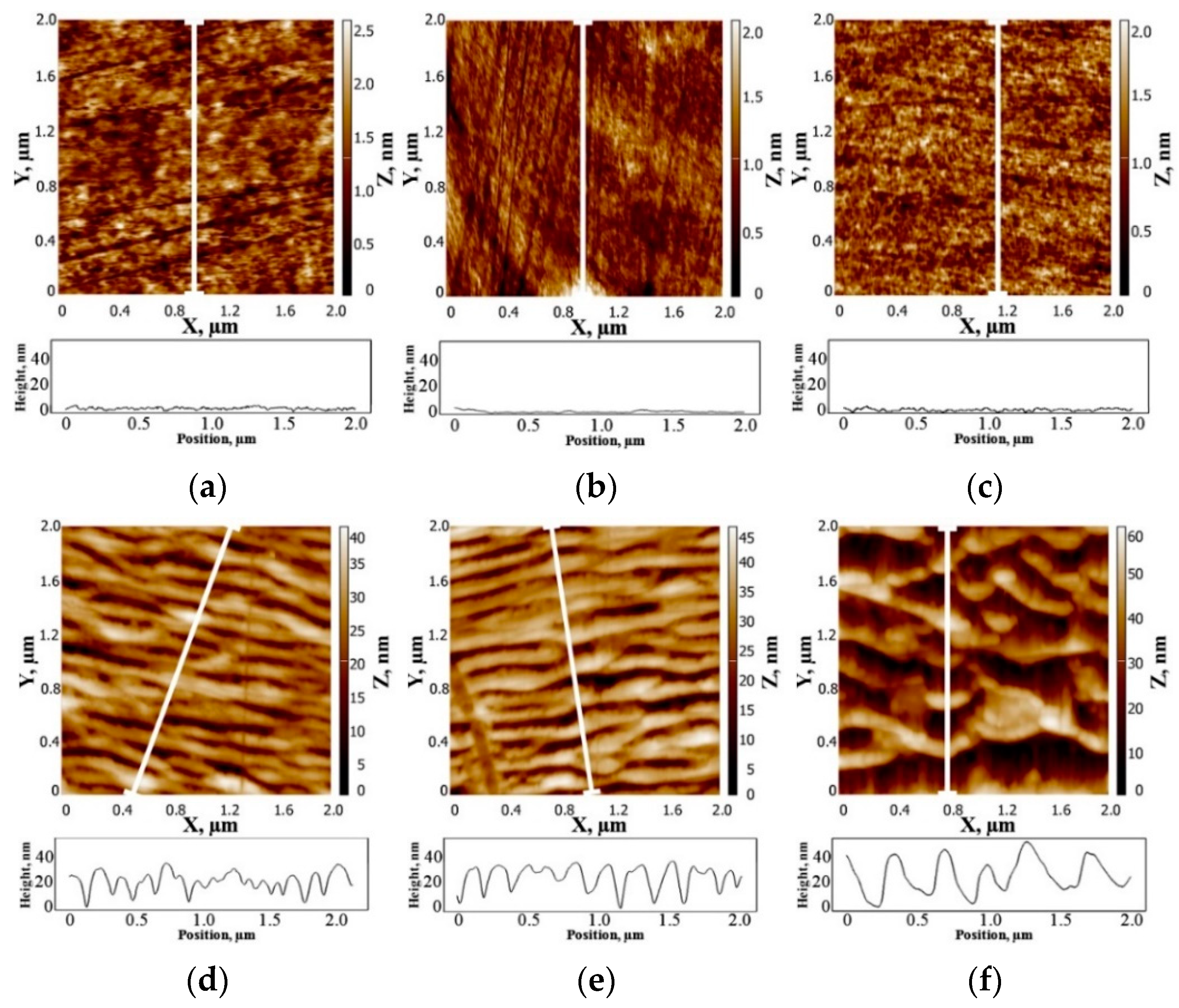
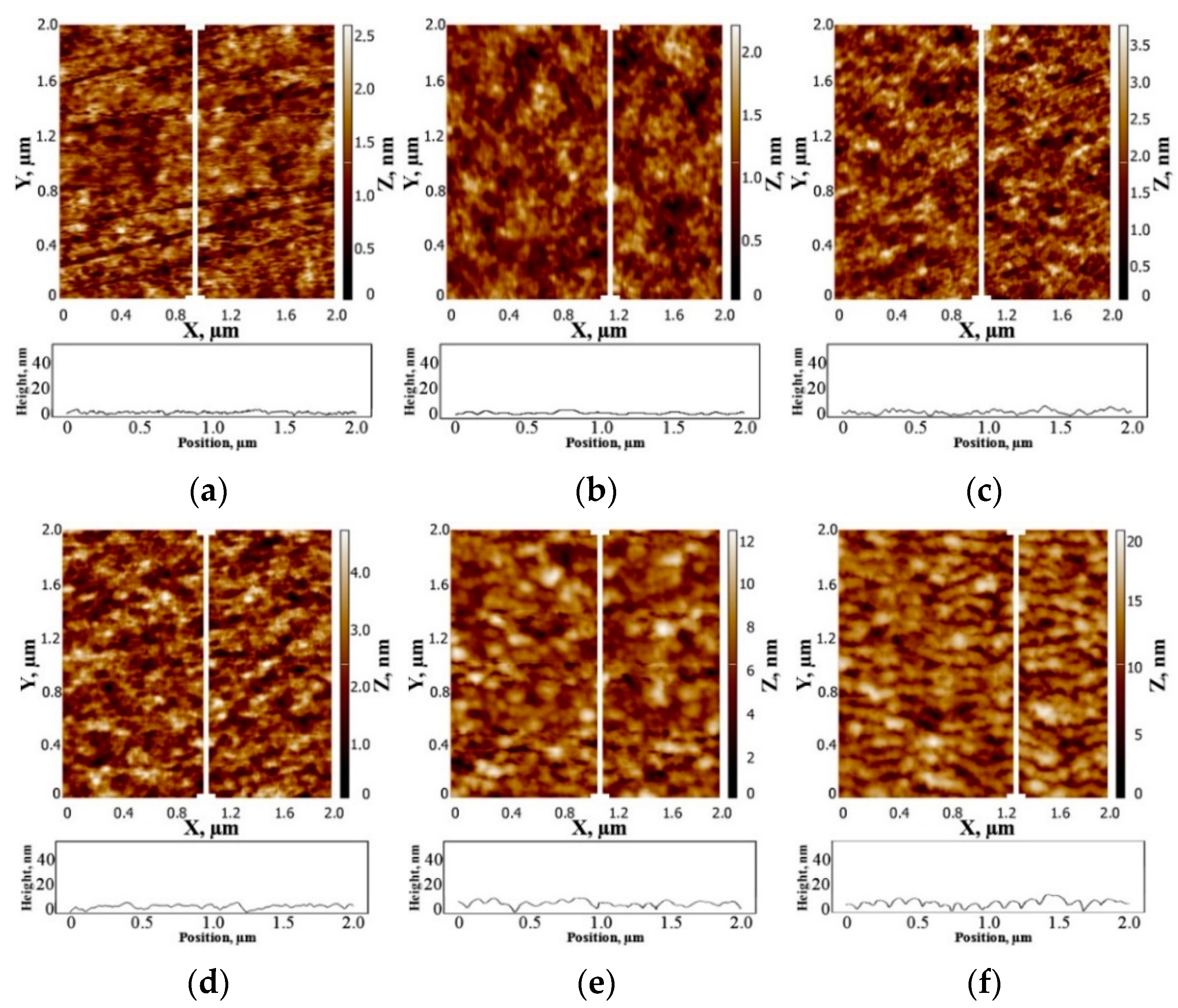
The maximum ion fluencies were 2 × 10¹⁶ ions/cm2 in the low-energy mode (Figure 1) and 3 × 10¹⁵ ions/cm2 in the high-energy mode (Figure 2). Despite the fact that the ion fluence in the high-energy mode was an order of magnitude lower, we assume that it is more correct to compare at the same etching depths because the formed nanostructures are nothing more than displaced surface material [8,9,10,11]. An aperture mask was used to estimate the etching depth and to obtain many processed areas (with different angles of incidence) on one sample. After processing, a step was formed at the “processed region–unprocessed region” boundary, the height of which was measured by AFM. The average etching depth ⟨Hetching⟩ was estimated from measurements in 9 areas of the formed step. The average etching depths were close—⟨Hetching⟩1 = 40 nm for low-energy mode and ⟨Hetching⟩2 = 55 nm for high-energy mode.
Figure 1 shows 2D images and profiles of the KTP surface as-prepared and after processing by argon cluster ions at the low-energy mode (E/Nmean = 12.5 eV/atom) at the different incident angles. The lowest point of the profile corresponds to Z = 0 nm. A slight change in the surface profile is observed after treatment at the incident angles less than 45°, and the maximum height Rt decreases from 2.5 to 2 nm. At larger incident angles (≥45°), the maximum height Rt increases significantly (by 16–24 times compared to the original surface) due to the formation of periodic nanostructures. As can be seen in Figure 1, the highest height of ripples is observed at the incident angle of 70° (Figure 1f) but the most ordered (including laterally) ripples—at 45° and 60° (Figure 1d,e). For clarity of differences in profiles both at different angles and for different treatment modes, the maximum height on the scale (in Figure 1 and Figure 2) is selected according to the height of the highest surface profile (Figure 1f). As it is shown in Ref. [18], such nanostructures contribute to the quality improvement of the antireflective coatings.
Figure 2 shows 2D images and profiles of the KTP surface as-prepared and after processing by argon cluster ions at the high-energy mode (E/Nmean = 110 eV/atom). First, periodic nanostructures are not observed even at incident angles of 45° and 60° (Figure 2d,e). Second, the maximum height of ripples is 10 nm at 70° (Figure 2f)—by 3 times lower than in low-energy mode. At first glance, it would seem that the high-energy treatment mode has better formation of periodic nanostructures due to high cluster energy. As seen in Figure 2, this is not the case.
We assume that this is due to the significant difference in sputtering yields of the two treatment modes—by 36 times: 100 cluster ions with E/Nmean = 110 eV/atom sputter 72 target atoms and 100 cluster ions with E/Nmean = 12.5 eV/atom sputter only 2 target atoms. Thus, a large proportion of cluster energy at the low-energy mode is spent not only on sputtering (low sputtering yield) but also on the active lateral displacement of subsurface target atoms, i.e., the formation of periodic nanostructures.
3.2. Power Spectral Density Functions
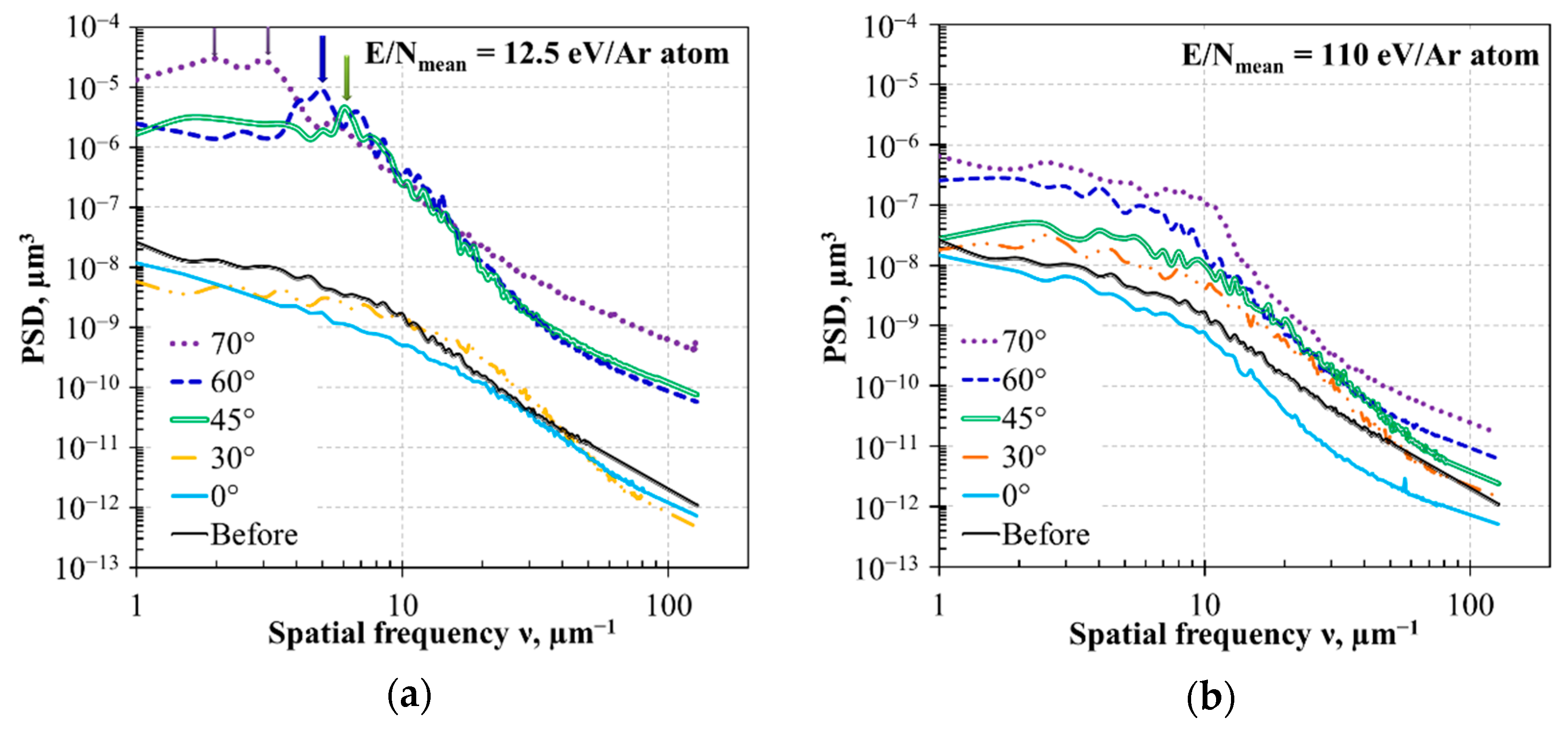
Figure 3 demonstrates the PSD functions of the KTP surface after processing at the different incident cluster angles for both treatment modes. In contrast to AFM images, PSD functions provide more quantitative data, especially for nanostructures. As can be seen in Figure 3a, low-energy mode smooths the KTP surface at small angles (≤30°) in the wide range of spatial frequencies ν from 1 to 8 μm−1 (30°) and to 15 μm−1 (0°). The self-organized nanostructures increase the surface roughness over the whole range of spatial frequencies. In Figure 3a, the pronounced peaks (marked by arrows) are observed. Each peak characterizes the frequency of self-organized nanostructures. It should be noted that the peak shift corresponds to the change of characteristic size (wavelength) of the nanostructure, which increases with increasing the incident angle, i.e., 167, 200, 334–500 nm for 45°, 60°, and 70°, respectively. PSD functions of high-energy mode are fundamentally different from the previous mode. First, the cluster ions with E/Nmean = 110 eV/atom at the incident angle of 0° better smooth the surface irregularities with the spatial frequency ν above 15 μm−1, but worse smooth—with ν < 15 μm−1. At the incident angles of 45–70°, PSD peaks are not observed and all functions are below low-energy-functions. This corresponds to a smoother surface in whole range of spatial frequencies ν and the absence of even weakly pronounced periodic nanostructures. Thus, the nanostructures observed on AFM images (Figure 2e,f) are nonperiodic, because they have different spatial frequencies ν in accordance with the PSD-data.
Table 1 shows a comparison of effective roughness parameter σeff and RMS roughness parameter Rq. At both treatment modes, the surface roughness decreases to 0.28–0.30 nm at small angles (≤30°) and then significantly increases to several nanometers. It should be noted that effective roughness σeff is higher than RMS roughness Rq at low-energy mode (8–9.7%), which is most likely due to the allowance for the lateral roughness of periodic nanostructures.
4. Conclusions
The influence of fundamentally different treatment modes by the argon cluster ions on the nanostructure formation on the surface of KTP single crystals has been investigated experimentally. At normal incidence of low- and high-energy cluster ions, the surface roughness decreases to 30%. The ordered nanostructures were not observed after processing by the high-energy cluster ions (E/Nmean = 110 eV/atom) even at slightly higher etching depths (compared to low-energy mode) and at the small angles (≤30°) of incidence of the cluster ions with E/Nmean = 12.5 eV/atom. It is assumed that the treatment by cluster ions with low energy leads to the formation of periodic nanostructures since the energy is insufficient for efficient sputtering of the target, but sufficient for a significant lateral displacement of subsurface target atoms. The most ordered nanostructures are formatted at the surface processing at angles of 45° and 60°, and they have a wavelength of 167 and 200 nm, respectively. One of the applications is the formation of periodic nanostructures on substrates of antireflective coatings to improve their quality.
Author Contributions
Conceptualization, I.V.N. and N.G.K.; methodology, N.G.K.; data acquisition, I.V.N. and N.G.K.; data processing, I.V.N.; original draft preparation, I.V.N.; review and editing, N.G.K.; visualization, I.V.N.; supervision, N.G.K. All authors have read and agreed to the published version of the manuscript.
Funding
This research was funded by the Ministry of Science and Higher Education of the Russian Federation, grant number FSUS-2020-0039.
Institutional Review Board Statement
Not applicable.
Informed Consent Statement
Not applicable.
Data Availability Statement
Data is contained within the article.
Acknowledgments
The authors acknowledge the NSU Shared Equipment Center “Applied Physics.”
Conflicts of Interest
The authors declare no conflict of interest. The funders had no role in the design of the study; in the collection, analyses, or interpretation of data; in the writing of the manuscript; or in the decision to publish the results.
References
- Sorokina, N.I.; Voronkova, V.I. Structure and properties of crystals in the potassium titanyl phosphate family: A review. Crystallogr. Rep. 2007, 52, 80–93. [Google Scholar] [CrossRef]
- Mamrashev, A.; Nikolaev, N.; Antsygin, V.; Andreev, Y.; Lanskii, G.; Meshalkin, A. Optical Properties of KTP Crystals and Their Potential for Terahertz Generation. Crystals 2018, 8, 310. [Google Scholar] [CrossRef] [Green Version]
- Pohl, K.; Bartelt, M.C.; de la Figuera, J.; Bartelt, N.C.; Hrbek, J.; Hwang, R.Q. Identifying the forces responsible for self-organization of nanostructures at crystal surfaces. Nature 1999, 397, 238–241. [Google Scholar] [CrossRef]
- Frost, F.; Ziberi, B.; Höche, T.; Rauschenbach, B. The shape and ordering of self-organized nanostructures by ion sputtering. Nucl. Instr. Meth. Phys. Res. B 2004, 216, 9–19. [Google Scholar] [CrossRef]
- El-Atwani, O.; Ortoleva, S.; Cimaroli, A.; Allain, J.P. Formation of silicon nanodots via ion beam sputtering of ultrathin gold thin film coatings on Si. Nanoscale Res. Lett. 2011, 6, 403. [Google Scholar] [CrossRef] [PubMed]
- Ziberi, B.; Frost, F.; Höche, T.; Rauschenbach, B. Ion-induced self-organized dot and ripple patterns on Si surfaces. Vacuum 2006, 81, 155–159. [Google Scholar] [CrossRef]
- Barth, J.V.; Costantini, G.; Kern, K. Engineering atomic and molecular nanostructures at surfaces. Nature 2005, 437, 671–679. [Google Scholar] [CrossRef] [PubMed]
- Toyoda, N.; Mashita, T.; Yamada, I. Nano structure formation by gas cluster ion beam irradiation at oblique incidence. Nucl. Instr. Meth. Phys. Res. B 2005, 232, 212–216. [Google Scholar] [CrossRef]
- Toyoda, N.; Tilakaratne, B.; Saalem, I.; Chu, W.-K. Cluster beams, nano-ripples, and bio applications. Appl. Phys. Rev. 2019, 6, 020901. [Google Scholar] [CrossRef]
- Zeng, X.; Pelenovich, V.; Xing, B.; Rakhimov, R.; Zuo, W.; Tolstogouzov, A.; Liu, C.; Fu, D.; Xiao, X. Formation of nanoripples on ZnO flat substrates and nanorods by gas cluster ion. Beilstein J. Nanotech. 2020, 11, 383–390. [Google Scholar] [CrossRef] [PubMed]
- Ieshkin, A.; Kireev, D.; Ozerova, K.; Senatulin, B. Surface ripple induced by gas cluster ion beam on copper surface at elevated temperatures. Mater. Lett. 2020, 272, 127829. [Google Scholar] [CrossRef]
- Korobeishchikov, N.G.; Nikolaev, I.V.; Roenko, M.A. Effect of argon cluster ion beam on fused silica surface morphology. Nucl. Instr. Meth. Phys. Res. B 2019, 438, 1–5. [Google Scholar] [CrossRef]
- Korobeishchikov, N.G.; Skovorodko, P.A.; Kalyada, V.V.; Shmakov, A.A.; Zarvin, A.E. Experimental and Numerical Study of High Intensity Argon Cluster Beams. AIP Conf. Proc. 2014, 1628, 885–892. [Google Scholar]
- Korobeishchikov, N.G.; Kalyada, V.V.; Skovorodko, P.A.; Shmakov, A.A.; Khodakov, M.D.; Shulzhenko, G.I.; Voskoboynikov, R.V.; Zarvin, A.E. Features of formation of gas cluster ion beams. Vacuum 2015, 119, 256–263. [Google Scholar] [CrossRef]
- Duparre, A.; Ferre-Borrull, J.; Gliech, S.; Notni, G.; Steinert, J.; Bennett, J.M. Surface characterization techniques for determining the root-mean-square roughness and power spectral densities of optical components. Appl. Opt. 2002, 41, 154–171. [Google Scholar] [CrossRef] [PubMed] [Green Version]
- Persson, B.N.J.; Albohr, O.; Tartaglino, U.; Volokitin, A.I.; Tosatti, E. On the nature of surface roughness with application to contact mechanics, sealing, rubber friction and adhesion. J. Phys. Condens. Matter 2005, 17, R1–R62. [Google Scholar] [CrossRef] [PubMed] [Green Version]
- Martínez, J.F.G.; Nieto-Carvajal, I.; Abad, J.; Colchero, J. Nanoscale measurement of the power spectral density of surface roughness: How to solve a difficult experimental challenge. Nanoscale Res. Lett. 2012, 7, 174. [Google Scholar] [CrossRef] [PubMed] [Green Version]
- Bushunov, A.A.; Tarabrin, M.K.; Lazarev, V.A.; Karasik, V.E.; Korostelin, Y.V.; Frolov, M.P.; Skasyrsky, Y.K.; Kozlovsky, V.I. Fabrication of anti-reflective microstructures on chalcogenide crystals by femtosecond laser ablation. Opt. Mat. Express 2019, 9, 1689–1697. [Google Scholar] [CrossRef]
Figure 1.
Atomic force microscopy (AFM) images and profiles of potassium titanyl phosphate (KTP) surface before (a) and after the low-energy treatment mode at different incident angles of cluster ions: (b) 0°, (c) 30°, (d) 45°, (e) 60°, and (f) 70°.
Figure 1.
Atomic force microscopy (AFM) images and profiles of potassium titanyl phosphate (KTP) surface before (a) and after the low-energy treatment mode at different incident angles of cluster ions: (b) 0°, (c) 30°, (d) 45°, (e) 60°, and (f) 70°.

Figure 2.
AFM images and profiles of KTP surface before (a) and after the high-energy treatment mode at different incident angles of cluster ions: (b) 0°, (c) 30°, (d) 45°, (e) 60°, and (f) 70°.
Figure 2.
AFM images and profiles of KTP surface before (a) and after the high-energy treatment mode at different incident angles of cluster ions: (b) 0°, (c) 30°, (d) 45°, (e) 60°, and (f) 70°.

Figure 3.
Power spectral density (PSD) functions of KTP surface at different incident angles of cluster ions: (a) after low-energy mode and (b) after high-energy mode.
Figure 3.
Power spectral density (PSD) functions of KTP surface at different incident angles of cluster ions: (a) after low-energy mode and (b) after high-energy mode.


Table 1.
Comparison of roughness parameters.
| Treatment Mode | Roughness Parameter | Before | Incident Angle of Clusters | ||||
|---|---|---|---|---|---|---|---|
| 0° | 30° | 45° | 60° | 70° | |||
| Low-energy mode | ⟨Rq⟩, nm | 0.40 | 0.28 | 0.28 | 6.2 | 7.5 | 12.6 |
| ⟨σeff⟩, nm | 0.43 | 0.28 | 0.30 | 6.8 | 8.1 | 13.8 | |
| High-energy mode | ⟨Rq⟩, nm | 0.40 | 0.30 | 0.56 | 0.75 | 1.7 | 2.8 |
| ⟨σeff⟩, nm | 0.43 | 0.30 | 0.60 | 0.83 | 1.8 | 2.7 | |
Publisher’s Note: MDPI stays neutral with regard to jurisdictional claims in published maps and institutional affiliations. |
© 2021 by the authors. Licensee MDPI, Basel, Switzerland. This article is an open access article distributed under the terms and conditions of the Creative Commons Attribution (CC BY) license (http://creativecommons.org/licenses/by/4.0/).
Share and Cite
MDPI and ACS Style
Nikolaev, I.V.; Korobeishchikov, N.G. Influence of the Parameters of Cluster Ions on the Formation of Nanostructures on the KTP Surface. Appl. Nano 2021, 2, 25-30. https://0-doi-org.brum.beds.ac.uk/10.3390/applnano2010003
AMA Style
Nikolaev IV, Korobeishchikov NG. Influence of the Parameters of Cluster Ions on the Formation of Nanostructures on the KTP Surface. Applied Nano. 2021; 2(1):25-30. https://0-doi-org.brum.beds.ac.uk/10.3390/applnano2010003
Chicago/Turabian StyleNikolaev, Ivan V., and Nikolay G. Korobeishchikov. 2021. "Influence of the Parameters of Cluster Ions on the Formation of Nanostructures on the KTP Surface" Applied Nano 2, no. 1: 25-30. https://0-doi-org.brum.beds.ac.uk/10.3390/applnano2010003