
High-Throughput Nanoparticle Chemisorption Printing of Chemical Sensors with High-Wiring-Density Electrodes


Research Institute for Advanced Electronics and Photonics (RIAEP), National Institute of Advanced Industrial Science and Technology (AIST), 1-1-1 Higashi, Tsukuba 305-8565, Japan
Electron. Mater. 2021, 2(2), 72-81; https://0-doi-org.brum.beds.ac.uk/10.3390/electronicmat2020007
Submission received: 4 March 2021
/
Revised: 30 March 2021
/
Accepted: 6 April 2021
/
Published: 8 April 2021
Abstract
:We report on the high-throughput non-lithographic microprinting of a high-wiring-density interdigitated array electrode (line and space = 5 µm/5 µm), based on a facile wet/dewet patterning of silver nanoparticle ink. The trade-off between high-density wiring and pattern collapse in the wet/dewet patterning is overcome by employing a new herringbone design of interdigitated array electrode. We demonstrate electrochemical sensing of p-benzoquinone by the fabricated interdigitated array electrode, showing a typical steady-state I–V characteristics with superior signal amplification benefiting from the redox cycling effect. Our findings provide a new technical solution for the scalable manufacture of advanced chemical sensors, with an economy of scale that cannot be realized by other techniques.
1. Introduction
Chemical sensors that convert a chemical or physical property of a specific analyte into a measurable signal are widely used for gas sensing, biosensing, ion sensing, and so on [1,2,3,4,5]. They have become increasingly important with the recent advances in big data analytics, which requires various data sources to obtain very large diverse datasets [6,7,8]. The essential requirements of sensors in big data analytics are small size and high sensitivity, which enable them to be put anywhere to collect meaningful signals, exhaustively. Microelectronics plays a key role in the miniaturization and sensitivity improvement of chemical sensors. For example, it facilitates the miniaturization necessary for in vivo sensing of biochemical responses in tissues and intact organisms [9,10,11]. Moreover, miniaturized electrodes, such as interdigitated array electrodes with dimensions in micrometers, possess convergent analyte diffusion with enhanced mass transport that leads to significant amplification of the sensing signal during amperometric analysis [12,13]. Owing to the narrow gap between the interdigitated array electrodes, a redox species that is oxidized (or reduced) at one electrode can diffuse and be reduced (or oxidized) at the adjacent electrode, which allows multiple oxidative/reductive conversions of the same molecule, resulting in a strong signal amplification, named as the “redox cycling effect”.
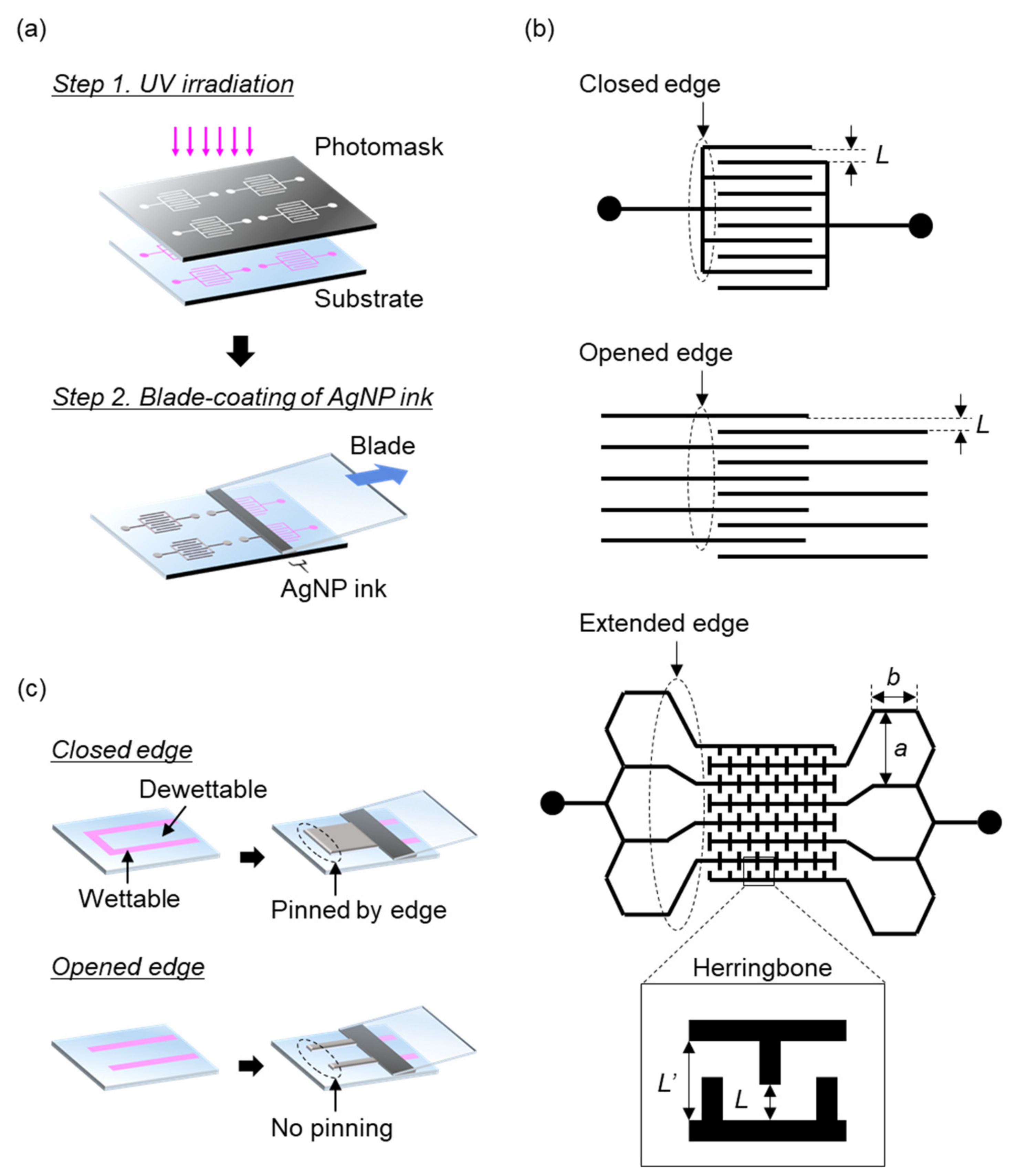
The fabrication of high-wiring-density interdigitated array electrodes is conducted by photolithography because it allows submicron-scale metal patterning with high reproducibility, using a patterned photoresist as a lift-off mask [14]. The photolithography is, however, an expensive multi-step process requiring high-precision mask alignment, which severely hinders the development and scale-up of microelectronic chemical sensors. By contrast, wet/dewet patterning, based on the spontaneous alignment of deposited materials as guided by the surface wettability of an underlying substrate, allows an alignment-free, high-throughput, and scalable approach for the manufacture of chemical sensors. Recently, ultrafine metal printing, based on wet/dewet patterning, was reported. The technique, named as nanoparticle chemisorption printing [15], utilizes a unique chemisorption effect of silver nanoparticles (AgNPs) and is composed of a simple two-step process: A patterned activated surface is prepared by irradiating a perfluoropolymer surface with vacuum ultraviolet (VUV) light through a photomask and is then exposed to the AgNP ink by blade coating (Figure 1a). This technique enables facile and high-throughput fabrication of an ultrafine silver pattern with a minimum line width of 0.8 µm and can be utilized to manufacture a transparent touch screen sensor [15,16]. However, it is still challenging to fabricate a complicated high-wiring-density metal pattern, as with interdigitated array electrodes with no line collapse.
Here, we report on the facile and high-throughput fabrication of high-wiring-density interdigitated array electrodes, based on wet/dewet patterning with micron-scale spatial resolution. High-wiring-density interdigitated array electrodes, with line and space of 5 µm/5 µm, were successfully fabricated by the nanoparticle chemisorption printing of an AgNP ink onto a hydrophobic perfluoropolymer surface. We show a design rule for a wet/dewet pattern, enabling fabrication of high-wiring-density interdigitated array electrodes with no line collapse. Furthermore, we demonstrate the high-sensitivity electrochemical sensing of p-benzoquinone, whose derivatives are environmental pollutants toxic to human health [17], by the fabricated interdigitated array electrode, showing typical steady-state I–V characteristics with a signal amplification factor of approximately 6 benefiting from the redox cycling effect.
2. Methods
The perfluoropolymer, CYTOP CTL-809M, and p-benzoquinone were purchased from Asahi Glass Co., Ltd., Tokyo, Japan and TCI Co., Ltd., Tokyo, Japan, respectively. 50 wt% of AgNP ink was synthesized by the thermal decomposition of oxalate-bridging silver alkyl-amine complexes dispersed in 4:1 octane and butanol [18]. The fabrication of interdigitated array electrodes by nanoparticle chemisorption printing was examined for three different electrode designs; a closed-edge design, an opened-edge design, and an extended-edge design (henceforth referred to as “closed edge”, “opened edge”, and “extended edge”, respectively), as shown in Figure 1b. Firstly, the CYTOP CTL-809M was spin-coated onto a glass substrate at 3000 rpm and dried at 453 K, for 30 min, to form a perfluoropolymer layer with a thickness of 700 nm. Next, the perfluoropolymer layer was irradiated by an Xe2 excimer lamp, with a wavelength of 172 nm (VUS-3150, ORC manufacturing, Tokyo, Japan), through a photomask, to prepare a patterned reactive surface (Figure 1a). Then, the patterned reactive surface was exposed to the AgNP ink by blade-coating, with a coating speed of 0.5 to 5 mm s−1, resulting in the spontaneous formation of a silver pattern on the irradiated surface, after a coating blade was swept across it, while the unirradiated surface remained bare. Finally, the silver pattern was annealed at 353 K, for 30 min. The surface morphology and electric conductivity of the interdigitated array electrodes were examined by an atomic force microscope (AFM) (Dimension 3100, Digital Instruments, Inc., Santa Barbara, CA, USA) and a semiconductor device analyzer (E5270, Agilent Technologies, Inc., Santa Clara, CA, USA), respectively. Electrochemical measurements were performed, using an electrochemical workstation (CompactStat, Ivium Technologies B. V., Eindhoven, Netherlands), with the interdigitated array electrodes as the working electrodes, a platinum wire as the counter electrode, and an Ag/AgCl electrode as the reference electrode. The measurements were carried out for an aqueous solution of p-benzoquinone, containing 100 mM tetraethylammonium tetrafluoroborate as a supporting electrolyte. Cyclic voltammetry was performed by applying 1 mL of the p-benzoquinone solution (0.01–100 μM and 10 mM) onto the interdigitated array electrodes and measured at voltage range between −0.5 and 0.1 V vs. Ag/AgCl under unstirred condition.
3. Results and Discussion
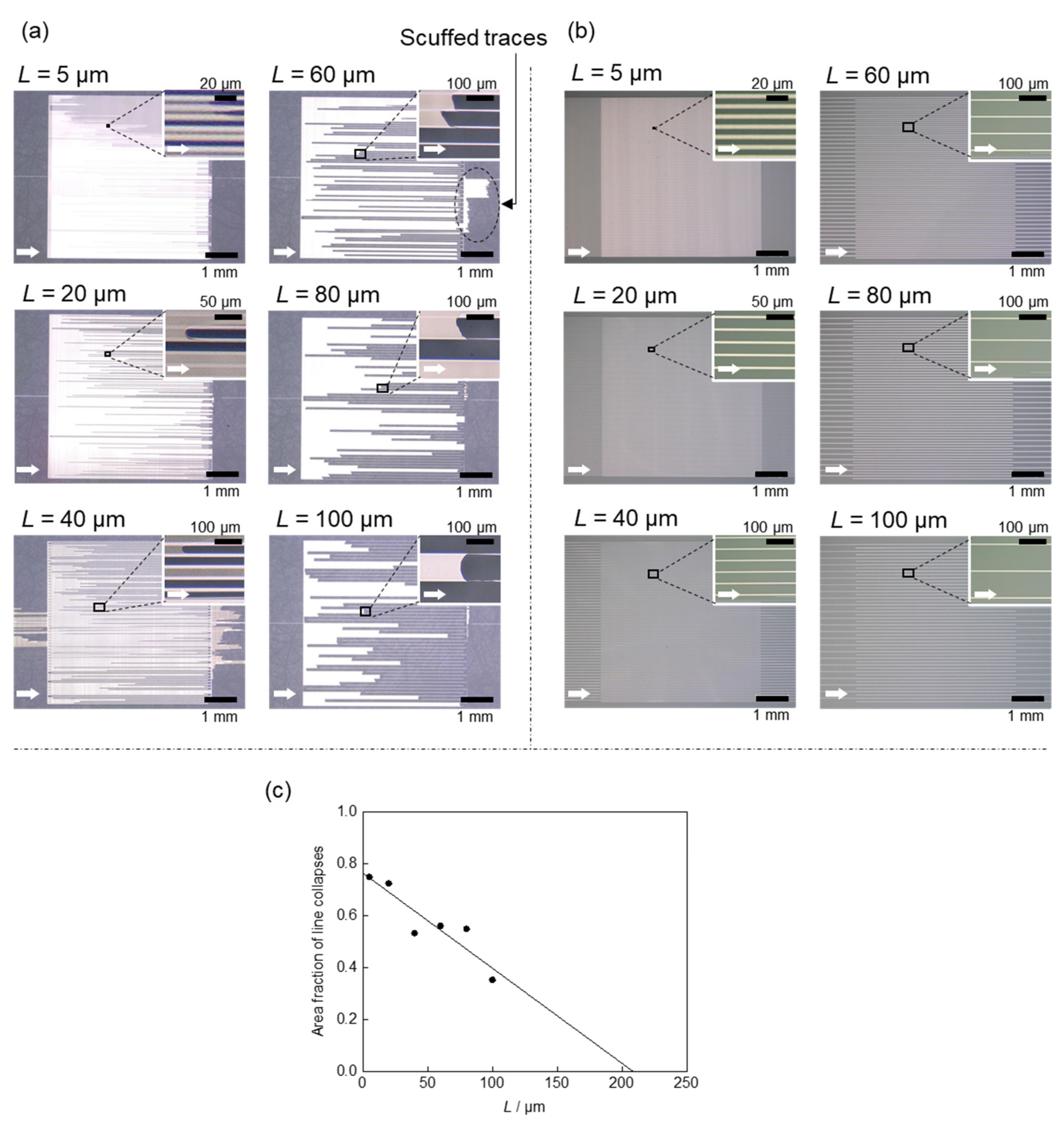
Figure 2a shows the results of the nanoparticle chemisorption printing for the closed edge, on which the silver patterns were coated by sweeping a blade from left to right in the images. The electrode width was fixed at 5 μm and the electrode gap (L) was systematically changed from 5 to 100 μm. As indicated in the figure, scuffed traces were observed at the right edge of the interdigitated array electrodes, due to pinning of the ink by the right edge line, perpendicular to the blade-sweep axis. Furthermore, line collapses were observed in a wide area of the interdigitated array electrodes, associated with pinning of the ink by the left edge line, perpendicular to the blade-sweep axis. Such serious line collapses may be ascribed to the phenomenon that wettable lines surrounding a dewettable region strongly pin ink, as shown in Figure 1c. As the evidence shows, no pattern collapses were observed, even at L = 5 μm, in the case of the opened edge (Figure 2b), which did not have wettable lines surrounding the dewettable region (Figure 1c). The area fraction of line collapses in the closed edge tended to decrease with an increase of L, while it could not be eliminated completely, even at L = 100 μm. By extrapolating the dependence of the area fraction on L, it was estimated that, at least, L should be larger than 200 μm, to eliminate line collapses completely (Figure 2c).
To clarify the design rule of a wet/dewet pattern enabling the fabrication of high-wiring density interdigitated array electrodes with no line collapse, we consider the interfacial free energy [19] for a simple closed edge model, as shown in Figure 3. Assuming that the line collapse occurs as shown by the pinning state in Figure 3, the total interfacial free energy () of the region, indicated by the dotted line, can be expressed as follows:
where , , and are interfacial free energies for the liquid-gas interface, the solid (dewettable)–liquid interface and the solid (wettable)–liquid interface, respectively. Moreover, h and G correspond to the thickness of a liquid film and the gap between adjacent wettable lines, respectively; x is the distance between the front edge of a blade and the pinning edge of an ink. On the other hand, assuming that the line collapse does not occur as shown in the non-pinning state depicted in Figure 3, the total interfacial free energy () can be expressed as follows:
where is the interfacial free energy for the solid (dewettable)–gas interface. From Equations (1) and (2), the energy difference between the pinning and non-pinning states can be obtained as follows:
where is a liquid contact angle on the dewettable solid surface. To obtain the non-pinning state stably, the Equation (3) must satisfy the conditions, and . These conditions give the following equations:
From Equation (5), it was found that G and should be larger and h should be smaller, to obtain the non-pinning state stably. The nanoparticle chemisorption printing in this study was performed with h = 35 μm, which was controlled by the height of the blade from a substrate. of AgNP ink on the Cytop layer is 37° [15]. Inputting these experimental parameters to Equations (4) and (5) gives G > 200 μm and x ≥ 26 mm, where the former is consistent with the experimental estimation of L = 200 μm, as shown in Figure 2c. The latter indicates that the blade must be swept more than 26 mm from a pinning edge of ink to eliminate a line collapse, although, in practical experiments, ink will dry before sweeping 26 mm. The realistic condition of the practical experiments can be obtained as x ≥ 600 μm, by setting G = 300 μm in Equation (4).
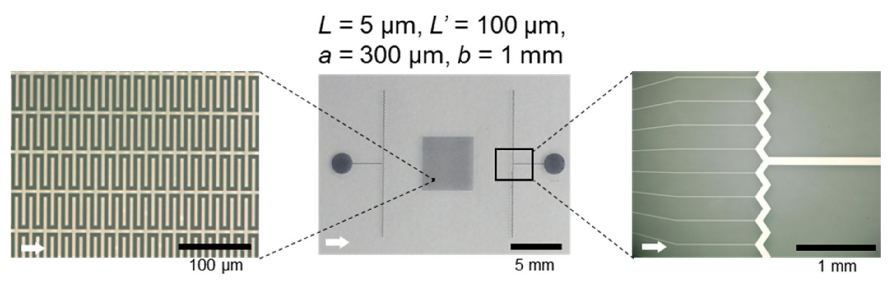
On the basis of the parameters estimated in the previous paragraph, we designed a new wet/dewet pattern of interdigitated array electrodes (see the extended edge in Figure 1b). In this pattern, the edge region with the length of b = 1 mm has the electrode gap extended to a = 300 µm, where a and b satisfy the requirements, G = 300 μm and x ≥ 600 μm, to eliminate line collapses. On the other hand, the central region should have a small electrode gap (L) to achieve better sensitivity in chemical sensor applications, while a small L leads to a large ratio of a/L, resulting in a misshapen electrode shape; for example, L = 5 µm gives a/L = 300/5, meaning that the edge region is 60 times larger than the central region. To avoid this problem, we employed a herringbone-like electrode design with L = 5 µm and L’ = 100 µm for the central region (Figure 1b), which enables a/L’ = 300/100, a small value, even at L = 5 µm. Furthermore, to avoid the scuffed traces found in Figure 2a, we introduced a zigzag shape into the edge line. This design is composed of tilted lines with respect to the blade-sweep axis, which is effective for eliminating the ink pinning in a line perpendicular to the blade-sweep axis. Figure 4 shows a result of the nanoparticle chemisorption printing for the extended edge with L = 5 µm. It can be clearly seen that the high-wiring-density interdigitated array electrodes were successfully fabricated with no line collapse and no scuffed trace, indicating that the new design is quite effective for eliminating these patterning errors. The coating speed of 0.5 mm s−1 took 44 s to fabricate the interdigitated array electrodes, with a dimension of 22.0 mm × 13.7 mm; it is possible to scale-up the process with high-throughput parallel printing.
Characterization of the fabricated interdigitated array electrodes, with L = 5 µm, was carried out by AFM, SEM, and conductivity measurements. Figure 5a shows an AFM image taken for a herringbone-like silver pattern of the electrodes. As seen, the electrodes are homogeneously formed with line and space of 5 µm/5 µm and a thickness of 40 nm. Figure 5b presents an enlarged SEM image of the printed silver electrode surface. It was clearly observed that the AgNPs fused to form conductive pass. The conductivity was examined by using a test element group (TEG), which is printed together with the interdigitated array electrodes on the same substrate. Figure 5c shows that the results measured for the silver lines with a width of 5 to 50 µm and a length of 1 to 5 mm. The obtained I–V characteristics had good linearity, and the conductivity was obtained at 80 ± 5 kS cm−1 by linear fitting, which was comparable to the reported value (100 kS cm−1) [15].
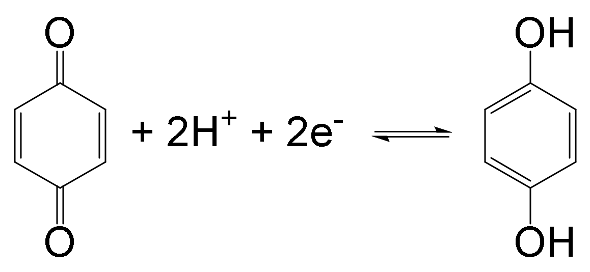
Electrochemical sensing by the fabricated interdigitated array electrodes was examined by measuring cyclic voltammograms of p-benzoquinone, which showed a reversible redox reaction as shown in Scheme 1 [20].
It is known that the application of interdigitated array electrodes to a reversible redox reaction induces current amplification, based on redox cycling effect [12,13]. The amplification factor strongly depends on the dimension of interdigitated array electrodes and can be considered as an indicator of the sensing capability [21]. As shown in Figure 5d, by applying a potential higher (or lower) than the redox potential of p-benzoquinone to the electrodes, W1 (or W2), of the interdigitated array electrodes, p-benzoquinone oxidized (or reduced) at W1 (or W2) can diffuse and be reduced (or oxidized) at W2 (or W1). This allows multiple oxidative/reductive conversions of p-benzoquinone, resulting in a strong redox current amplification. Such a redox cycling effect was examined by bipotentiostat-mode cyclic voltammetry, where a potential of W1 was swept in the voltage range of −0.5 to 0.1 V with fixing potential of W2 at 0.0 V. For comparison, normal measurements with no redox cycling effect were also performed by monopotentiostat-mode cyclic voltammetry, where the same potential was applied to W1 and W2 and was swept in the voltage range of −0.5 to 0.1 V. Figure 5e shows the results measured for 10 mM p-benzoquinone, using the interdigitated array electrodes (line and space of 5 µm/5 µm). The monopotentiostat-mode cyclic voltammogram showed typical, non-steady state I–V characteristics, with redox current peaks at −0.06 and −0.24 V for the forward and backward scans, respectively. In contrast, the bipotentiostat-mode cyclic voltammograms showed steady-state I–V characteristics with a constant current below −0.3 V, which is clear evidence of the redox cycling. Furthermore, the steady-state current of W1 (0.77 mA at −0.5 V) coincided very well with the theoretical value (0.71 mA), as calculated by the following equation [21]:
where m, b, n, F, c, D, w, and wg are number of electrodes, electrode length, number of electrons transferred in a redox reaction, Faraday constant, concentration of redox species, the diffusion coefficient of redox species (2.3 × 10⁻¹⁰ m2 s−1 for p-benzoquinone [22]), electrode width, and electrode gap, respectively. The amplification factor was estimated at 5.75 from the ratio between the steady-state current measured by the bipotentiostat mode and the non-steady state current measured by the monopotentiostat mode. The obtained amplification factor clearly indicates the capability of high-sensitivity chemical sensing for the fabricated interdigitated array electrodes. Figure 5f–i shows the current responses of the interdigitated array electrodes to 0.01–0.1, 0.1–1, 1–10, and 10–100 μM p-benzoquinone, respectively, measured by the bipotentiostat mode at the fixed potential of −0.3 V. As can be seen, a linear relationship was obtained for the range of 0.1–1 μM, 1–10 μM and 10–100 μM with sensitivity of 0.02527 ± 0.00227 A M−1, 0.02627 ± 0.00013 A M−1, and 0.02857 ± 0.00003 A M−1 and the corresponding R2 of 0.96093, 0.99988, and 0.99999, respectively. Such wide-range linearity and high sensitivity are likely benefits from the current amplification due to the redox cycling effect.
4. Conclusions
We showed high-throughput, non-lithographic microprinting of a high-wiring-density interdigitated array electrode, based on a facile wet/dewet patterning of silver nanoparticle ink. The patterning was performed for the closed- and opened-edge interdigitated array electrodes with systematically changing their electrode gap, and the results were analyzed by an interfacial free-energy model to clarify the requirements for eliminating patterning errors, such as line collapses and scuffed traces. Based on the obtained requirements, we designed a new extended-edge pattern with herringbone-like electrodes, which allowed the high-throughput wet/dewet patterning of high-wiring-density interdigitated array electrodes (line and space = 5 µm/5 µm) with no patterning error. Finally, we demonstrated the electrochemical sensing of p-benzoquinone by a fabricated interdigitated array electrode, showing superior signal amplification benefiting from the redox cycling effect.
Funding
This work was supported by Japan Society for the Promotion of Science (JSPS) KAKENHI grant number JP19H02587.
Institutional Review Board Statement
Not applicable.
Informed Consent Statement
Not applicable.
Data Availability Statement
The data presented in this study are available on request from the corresponding authors.
Acknowledgments
We are grateful to Gyo Kitahara and Tatsuo Hasegawa (Department of Applied Physics, The University of Tokyo) for their help in the nanoparticle chemisorption printing of interdigitated array electrodes.
Conflicts of Interest
The authors declare no conflict of interest.
References
- Seiyama, T. Chemical Sensor Technology; Kodansha Ltd.: Tokyo, Japan; Elsevier Science Publishers B.V.: Amsterdam, The Netherlands, 1988. [Google Scholar]
- Wang, C.X.; Yin, L.W.; Zhang, L.Y.; Xiang, D.; Gao, R. Metal Oxide Gas Sensors: Sensitivity and Influencing Factors. Sensors 2010, 10, 2088–2106. [Google Scholar] [CrossRef] [PubMed] [Green Version]
- Buhlmann, P.; Pretsch, E.; Bakker, E. Carrier-Based Ion-Selective Electrodes and Bulk Optodes. 2. Ionophores for Potentiometric and Optical Sensors. Chem. Rev. 1998, 98, 1593–1688. [Google Scholar] [CrossRef] [PubMed]
- Newman, J.D.; Turner, A.P.F. Home blood glucose biosensors: A commercial perspective. Biosens. Bioelectron. 2005, 20, 2435–2453. [Google Scholar] [CrossRef] [PubMed] [Green Version]
- Turner, A.P.F. Biosensors: Sense and sensibility. Chem. Soc. Rev. 2013, 42, 3184–3196. [Google Scholar] [CrossRef] [PubMed] [Green Version]
- Bandodkar, A.J.; Jeerapan, I.; Wang, J. Wearable Chemical Sensors: Present Challenges and Future Prospects. ACS Sens. 2016, 1, 464–482. [Google Scholar] [CrossRef]
- Kumar, J.R.R.; Pandey, R.K.; Sarkar, B.K. Pollutant gases detection using the machine learning on benchmark research datasets. Procedia Comput. Sci. 2019, 152, 360–366. [Google Scholar] [CrossRef]
- Cho, S.-Y.; Lee, Y.; Lee, S.; Kang, H.; Kim, J.; Choi, J.; Ryu, J.; Joo, H.; Jung, H.-T.; Kim, J. Finding hidden signals in chemical sensors using deep learning. Anal. Chem. 2020, 92, 6529–6537. [Google Scholar] [CrossRef] [PubMed]
- Wightman, R.M. Probing Cellular Chemistry in Biological Systems with Microelectrodes. Science 2006, 311, 1570–1574. [Google Scholar] [CrossRef] [Green Version]
- Lee, J.H.; Kim, H.; Kim, J.H.; Lee, S.H. Soft implantable microelectrodes for future medicine: Prosthetics, neural signal recording and neuromodulation. Lab Chip 2016, 16, 959–976. [Google Scholar] [CrossRef] [PubMed]
- Meng, L.; Turner AP, F.; Mak, W.C. Soft and flexible material-based affinity sensors. Biotechnol. Adv. 2020, 39, 107398. [Google Scholar] [CrossRef] [PubMed]
- Goluch, E.D.; Wolfrum, B.; Singh, P.S.; Zevenbergen, M.A.G.; Lemay, S.G. Redox cycling in nanofluidic channels using interdigitated electrodes. Anal. Bioanal. Chem. 2009, 394, 447–456. [Google Scholar] [CrossRef] [PubMed] [Green Version]
- Niwa, O.; Xu, Y.; Halsall, H.B.; Heineman, W.R. Small-volume voltammetric detection of 4-aminophenol with interdigitated array electrodes and its application to electrochemical enzyme immunoassay. Anal. Chem. 1993, 65, 1559–1563. [Google Scholar] [CrossRef] [PubMed]
- Mamishev, A.V.; Sundara-Rajan, K.; Yang, F.; Du, Y.Q.; Zahn, M. Interdigital sensors and transducers. Proc. IEEE 2004, 92, 808–845. [Google Scholar] [CrossRef] [Green Version]
- Yamada, T.; Fukuhara, K.; Matsuoka, K.; Minemawari, H.; Tsutsumi, J.; Fukuda, N.; Aoshima, K.; Arai, S.; Makita, Y.; Kubo, H.; et al. Nanoparticle chemisorption printing technique for conductive silver patterning with submicron resolution. Nat. Commun. 2016, 7, 11402. [Google Scholar] [CrossRef] [PubMed] [Green Version]
- Kitahara, G.; Aoshima, K.; Tsutsumi, J.; Minemawari, H.; Arai, S.; Hasegawa, T. Low-voltage operation of organic thin-film transistors based on ultrafine printed silver electrodes. Org. Electron. 2017, 50, 426–428. [Google Scholar] [CrossRef]
- Delgado-Saborit, J.M.; Alam, M.S.; Pollitt KJ, G.; Stark, C.; Harrison, R.M. Analysis of atmospheric concentrations of quinones and polycyclic aromatic hydrocarbons in vapour and particulate phases. Atmos. Environ. 2013, 77, 974–982. [Google Scholar] [CrossRef]
- Itoh, M.; Kakuta, T.; Nagaoka, M.; Koyama, Y.; Sakamoto, M.; Kawasaki, S.; Umeda, N.; Kurihara, M. Direct Transformation into Silver Nanoparticles via Thermal Decomposition of Oxalate-Bridging Silver Oleylamine Complexes. J. Nanosci. Nanotechnol. 2009, 9, 6655–6660. [Google Scholar] [CrossRef] [PubMed]
- Defay, R.; Prigogine, I.; Bellemans, A. Surface Tension and Adsorption; Wiley: New York, NY, USA, 1966. [Google Scholar]
- Monge-Romero, I.C.; Suarez-Herrera, M.F. Electrocatalysis of the hydroquinone/benzoquinone redox couple at platinum electrodes covered by a thin film of poly(3,4-ethylenedioxythiophene). Synth. Met. 2013, 175, 36–41. [Google Scholar] [CrossRef]
- Aoki, K.; Morita, M.; Niwa, O.; Tabei, H. Quantitative analysis of reversible diffusion-controlled currents of redox soluble species at interdigitated array electrodes under steady-state conditions. J. Electroanal. Chem. 1988, 256, 269–282. [Google Scholar] [CrossRef]
- Jakobs, R.C.M.; Janssen, L.J.J.; Barendrecht, E. Hydroquinone oxidation and p-benzoquinone reduction at polypyrrole and poly-N-methylpyrrole electrode. Electrochim. Acta 1985, 30, 1313–1321. [Google Scholar] [CrossRef] [Green Version]
Figure 1.
(a) Schematic of nanoparticle chemisorption printing. (b) Schematic of interdigitated array electrodes with three different designs: closed edge, opened edge, and extended edge. (c) Schematic of ink pinning at the edge line perpendicular to the blade-sweep axis.
Figure 1.
(a) Schematic of nanoparticle chemisorption printing. (b) Schematic of interdigitated array electrodes with three different designs: closed edge, opened edge, and extended edge. (c) Schematic of ink pinning at the edge line perpendicular to the blade-sweep axis.

Figure 2.
Optical micrographs for different designs of interdigitated array electrodes fabricated by nanoparticle chemisorption printing: (a) closed edge and (b) opened edge. The white arrows indicate the blade-sweep direction during the nanoparticle chemisorption printing. (c) Area fraction of line collapses, plotted as a function of electrode gap (L).

Figure 3.
Schematic models of non-pinning and pinning states used for the interfacial free-energy calculation.
Figure 3.
Schematic models of non-pinning and pinning states used for the interfacial free-energy calculation.

Figure 4.
Optical micrographs for extended-edge interdigitated array electrodes fabricated by nanoparticle chemisorption printing. The white arrows indicate the blade-sweep direction during the nanoparticle chemisorption printing.
Figure 4.
Optical micrographs for extended-edge interdigitated array electrodes fabricated by nanoparticle chemisorption printing. The white arrows indicate the blade-sweep direction during the nanoparticle chemisorption printing.

Figure 5.
(a) Atomic force microscope (AFM) and (b) SEM images of interdigitated array electrodes with the extended edge design. (c) Electric conductance of interdigitated array electrodes plotted as a function of the electrode width. (d) Schematic of redox cycling by interdigitated array electrodes. (e) Cyclic voltammograms of 10 mM p-benzoquinone measured by the interdigitated array electrodes with line and space of 5 µm/5 µm. The black and red curves correspond to the results obtained by monopotentiostat mode and bipotentiostat mode, respectively. Current responses to (f) 0.01–0.1 µM, (g) 0.1–1 µM, (h) 1–10 µM, and (i) 10–100 µM p-benzoquinone measured by bipotentiostat mode.

Scheme 1.
Redox reaction of p-benzoquinone.

Publisher’s Note: MDPI stays neutral with regard to jurisdictional claims in published maps and institutional affiliations. |
© 2021 by the author. Licensee MDPI, Basel, Switzerland. This article is an open access article distributed under the terms and conditions of the Creative Commons Attribution (CC BY) license (https://creativecommons.org/licenses/by/4.0/).
Share and Cite
MDPI and ACS Style
Tsutsumi, J. High-Throughput Nanoparticle Chemisorption Printing of Chemical Sensors with High-Wiring-Density Electrodes. Electron. Mater. 2021, 2, 72-81. https://0-doi-org.brum.beds.ac.uk/10.3390/electronicmat2020007
AMA Style
Tsutsumi J. High-Throughput Nanoparticle Chemisorption Printing of Chemical Sensors with High-Wiring-Density Electrodes. Electronic Materials. 2021; 2(2):72-81. https://0-doi-org.brum.beds.ac.uk/10.3390/electronicmat2020007
Chicago/Turabian StyleTsutsumi, Jun’ya. 2021. "High-Throughput Nanoparticle Chemisorption Printing of Chemical Sensors with High-Wiring-Density Electrodes" Electronic Materials 2, no. 2: 72-81. https://0-doi-org.brum.beds.ac.uk/10.3390/electronicmat2020007