Article

Towards Sustainable Crossbar Artificial Synapses with Zinc-Tin Oxide

1
Department of Electrical and Computer Engineering, NOVA School of Science and Technology and CTS-UNINOVA, NOVA University Lisbon, Campus de Caparica, 2829-516 Caparica, Portugal
2
i3N/CENIMAT, Department of Materials Science, NOVA School of Science and Technology and CEMOP/UNINOVA, NOVA University Lisbon, Campus de Caparica, 2829-516 Caparica, Portugal
*
Authors to whom correspondence should be addressed.
Submission received: 18 March 2021 / Revised: 8 April 2021 / Accepted: 14 April 2021 / Published: 16 April 2021
(This article belongs to the Special Issue Feature Papers of Electronic Materials)

Abstract

:
In this article, characterization of fully patterned zinc-tin oxide (ZTO)-based memristive devices with feature sizes as small as 25 µm2 is presented. The devices are patterned via lift-off with a platinum bottom contact and a gold-titanium top contact. An on/off ratio of more than two orders of magnitude is obtained without the need for electroforming processes. Set operation is a current controlled process, whereas the reset is voltage dependent. The temperature dependency of the electrical characteristics reveals a bulk-dominated conduction mechanism for high resistance states. However, the charge transport at low resistance state is consistent with Schottky emission. Synaptic properties such as potentiation and depression cycles, with progressive increases and decreases in the conductance value under 50 successive pulses, are shown. This validates the potential use of ZTO memristive devices for a sustainable and energy-efficient brain-inspired deep neural network computation.

1. Introduction

With the technological landscape shifting towards big data applications, such as Internet of Things (IoT), the need to analyze and process large amounts of data in a quick and efficient manner has greatly increased in the past decade [1]. The typical Von-Neumann architecture used on most current systems requires that the processing and memory units are independent of each other and connected by a data bus. This means that although the processing power of these systems has been improved over the last few years, it is not possible to take advantage of all its capabilities due to the limited bandwidth of the data bus (Von-Neumann bottleneck). When taking scalability into account, these systems also pose a problem due to the decrease in performance that comes as a consequence of CMOS technology limitations [2]. The increase in operating frequency and device density would involve a higher power consumption and increased operating temperatures. For most neuromorphic applications such as pattern recognition, portable systems do not process their data locally but instead are connect to an external computer server (“cloud”) that handles the data processing. This implies not only large power consumption but also a possibly unsafe transfer of data that might be undesirable when handling sensitive information. As an alternative, brain-inspired neuromorphic computation systems have been presented. The human brain consists of computing elements (neurons) and memory elements (synapses) that are connected in a massive parallel architecture. This parallelism allows the brain to outperform modern processors in tasks such as data classification and pattern recognition while being considerably more power efficient [3]. In order to emulate this highly interconnected network, dense arrays of memristors have been proposed. These two-terminal devices have been shown to emulate a variety of synaptic properties such as potentiation and depression, which are key characteristics of artificial neural networks (ANNs) [4].
Both the industrial and research communities have recently started to take an interest in non-filamentary resistive switching [5,6]. This interest is in great part not only due to the analog switching behavior that is shown in area-dependent mechanisms, but also because filament formation and destruction is not needed for switching to occur, leading to better device reliability [7]. Amorphous oxide semiconductors (AOS) are ideal materials for non-filamentary-based resistive switching [8,9]. These materials allow for an easier and cheaper production process than current market technologies while maintaining compatibility with CMOS processes [10].
When taking neuromorphic applications such as pattern recognition into account, it was shown that a better accuracy is achieved due to a lower random telegraphic noise of area-dependent memristors, compared to filamentary systems [11]. Besides that, by applying AOS-based material as the resistive switching material, flexible and transparent substrates such as plastic or paper can be used due to low processing temperatures and conventional patterning methods [12], which are great advantages for applications such as IoT. The most prominent AOS material in recent literature has been indium-gallium-zinc oxide (IGZO) [12,13,14]. This material has shown synaptic operations which can be applied for both computing paradigms of deep neural networks (DNNs) and spiking neural networks (SNNs). However, due to indium and gallium both being critical raw materials, the use of zinc-tin oxide (ZTO) has started to be considered as a reliable substitute [15,16,17,18]. There are few reports on ZTO memristive devices with synaptic capabilities [19,20], and even fewer using exclusively ZTO as their switching medium [21,22], with all sharing a common bottom electrode configuration. Although patterned ZTO devices have previously been presented [23], synaptic emulation and area dependent switching was never achieved in a crosspoint configuration and the smallest device area has been reported as 100 µm². Table 1 sumarizes the current state of the art and relates it to the current work. It is also worth noting that materials with other possible resistive switching mechanisms have been reported such as photo-induced [24], electrolyte gated [25] and second- and third-order effects [26].
For real-world applications, device cross bar implementations are necessary. Therefore, the first step is to obtain reliable device characteristics where both electrode contacts are patterned in a cross-point configuration. In the current report, full patterning of the contact layers of the devices was completed by lift-off.
Formerly, we have shown that non-patterned ZTO devices with common bottom Pt electrodes operate in two different modes of resistive switching (RS) [18]: 1D or filamentary (which requires electroforming) and 2D or area-dependent RS. Here in this article, we are focused on the area-dependent resistive switching properties of the device where the electroforming is not required. The characteristic was introduced as 8-wise RS in the literature [29]. However, this implies the application of the voltage to the Schottky contact. In order to use a more universal terminology, the above-mentioned switching mode is referred to as “forward set”, since the set operation happens in the diode’s forward directions [17].

2. Materials and Methods
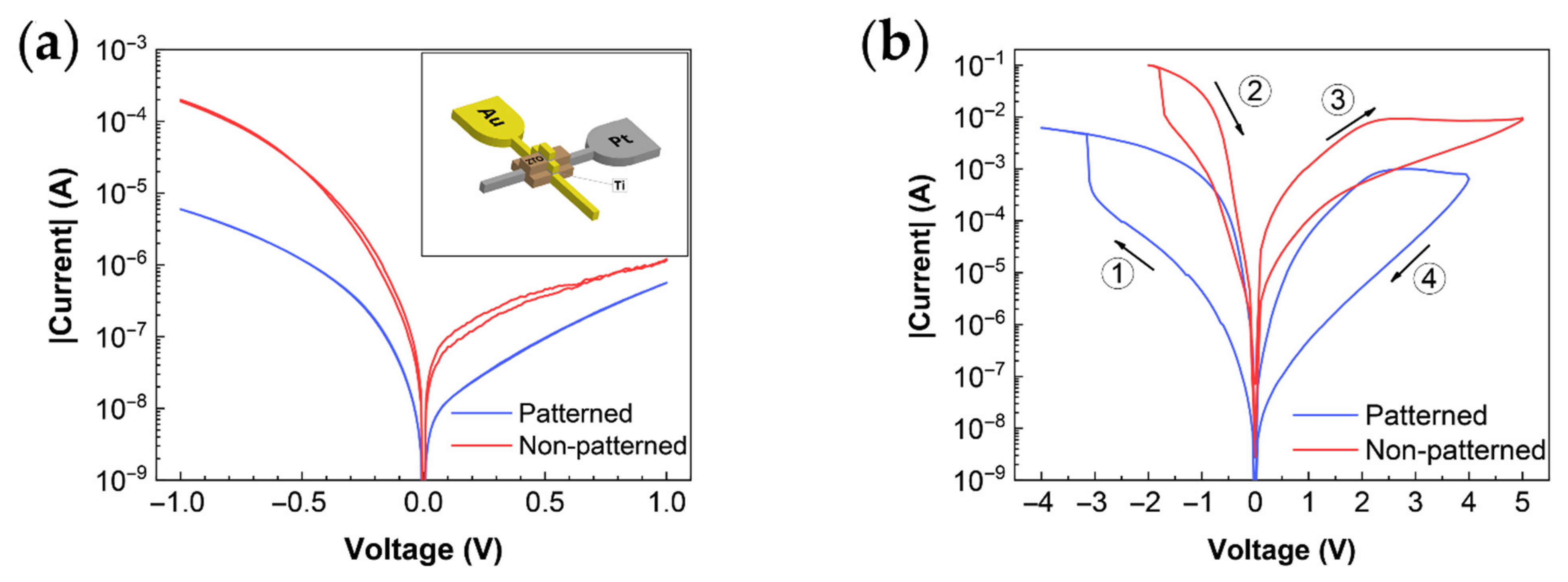
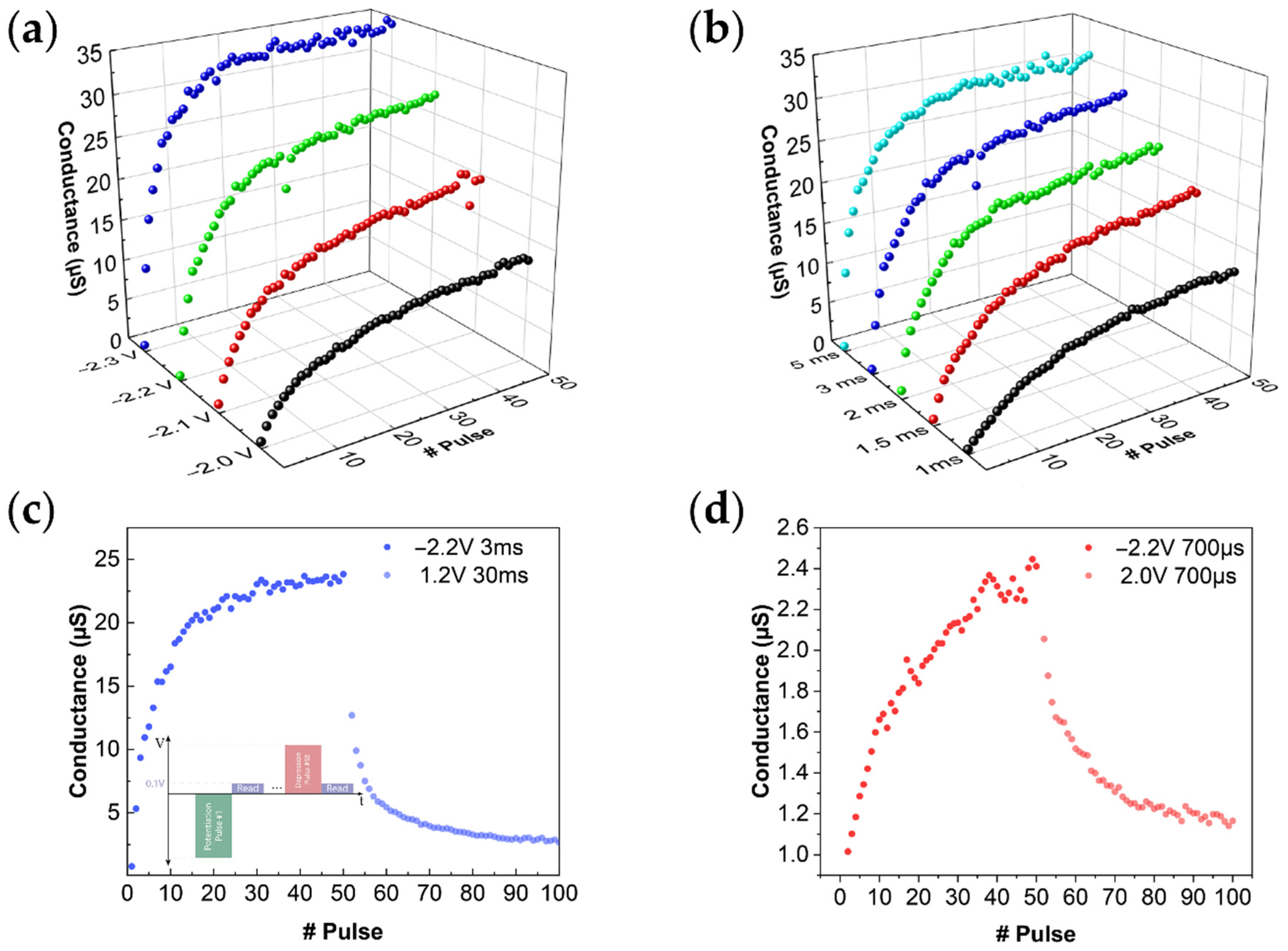
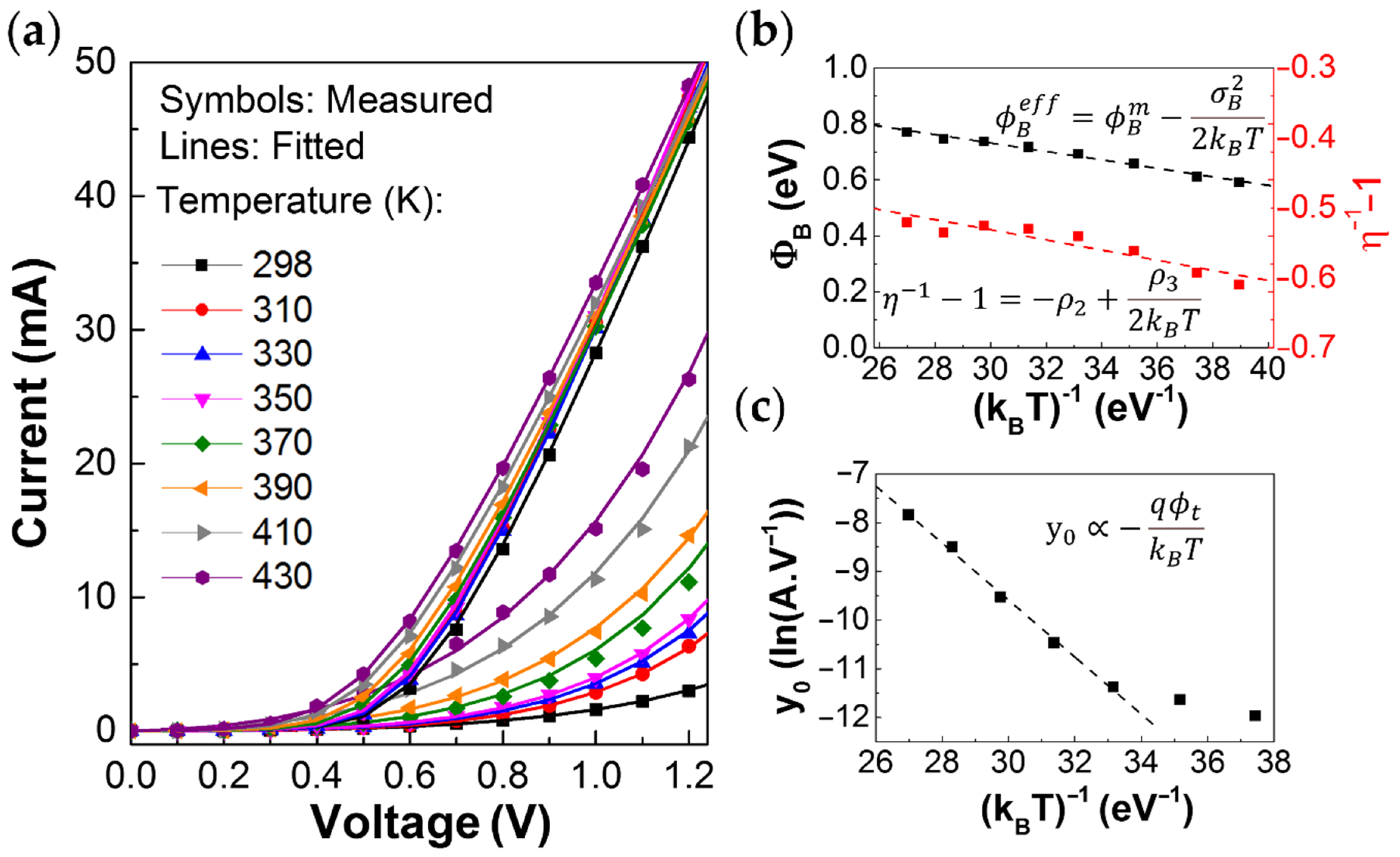
The fabrication of the presented ZTO memristive devices started with the patterning of the bottom electrodes via lift-off. E-beam evaporation was used for the deposition of 30 nm of Pt paired with another 30 nm thick layer of Ti that served as an adhesion layer between the substrate and the Pt. For surface cleaning purposes and to ensure a good rectification in the pristine state [18], an O2 plasma treatment was performed on the bottom electrode in situ moments before the deposition of the active layer. For this treatment, a substrate bias of 10 W was applied with a flow rate of 20 sccm of O2 for a duration of 10 min. For the active ZTO layer, the radio frequency (RF) magnetron sputtering process was used. The deposition was carried out at room temperature, with a flow rate of 20 sccm of Ar and 20 sccm of O2, an RF power of 160 W and a deposition pressure of 2.3 mTorr. Using these conditions, an 80 nm layer of ZTO was deposited in 18 min. For the top electrode, both deposition and patterning techniques were the same as the ones used for the bottom electrode. For this electrode, a 60 nm Au layer was deposited on top of a 6 nm Ti layer. After fabrication, the devices went through an annealing process of 120 °C for a period of 24 h.
The devices were measured in a dark environment, under ambient atmosphere, using a Keithley 4200-SCS semiconductor characterization system and a Janis ST-500 cryogenic probe station (Lake Shore Cryotronics, Westerville, OH, USA). The voltage was applied to the top electrode while the bottom electrode was grounded. For these conditions, the ZTO thin film presents an amorphous structure (Figure S1). X-ray diffraction (XRD) measurements were performed in a PANalytical’s X’Pert PRO diffractometer (Malvern Panalytical, Malvern, UK) using CuKα radiation with 2θ between 5° and 65° and a step size of 0.033°.

3. Results

All presented measurements were performed in 5 µm × 5 µm devices unless stated otherwise. The current–voltage (I–V) characteristics between −1 V and 1 V (pristine) of the patterned (area: 25 µm2) and non-patterned (area: 0.2 mm2) devices are presented in Figure 1a, along with a graphical illustration of the patterned device structure. The electrical characteristics of the patterned and non-patterned devices are similar, besides the different overall current level due to the device area. Additional area dependency of the resistance switching is shown in Figure S2. The polarity of the rectification reveals the presence of a Schottky-like barrier at the ZTO/Pt interface, as expected [18], while the Ti/Au interface is Ohmic. Hence, applying negative voltage (to the top electrode) corresponds to a forward biasing of the device. In Figure 1b, the direct current (DC) resistive switching behavior is shown. The current–voltage characteristics demonstrate the forward set bipolar switching nature of the device, with its set operation occurring under negative voltage bias, and the reset on the opposite polarity. The resistive switching window of the patterned devices is two orders of magnitude.
The forward set characteristic of ZTO memristive devices reveal retention loss [18]. The dynamic retention data is presented in Figure S3 This characteristic is beneficial for artificial neural networks, especially in sequence-to-sequence models [30].
Device endurance was initially tested by performing voltage sweeps between −4 and 4 V (Figure 2a); however, after the first few cycles, the device remained in the HRS, followed by an uncontrolled breakdown. Figure 2b shows a controllable resistive switching performance by combination of current sweep and voltage sweep for set and reset operations, respectively. This endurance plots are shown in a semi logarithmic scale in Figure S4. As shown in the Supporting Information, Figure S5, a higher maximum current range close to the values measured during voltage sweep does not negatively influence the cycle-to-cycle stability. The current-controlled set was already reported to lead to increased endurance for both valence change memory (VCM) and electrochemical memristor (ECM) cells [31].
In a biological brain, neurons communicate through synapses. Under stimulation of synapses by neural spikes, they update their strengths or weights, which are realized as potentiation and depression [32]. To replicate this behavior, pulsed signals were applied to the ZTO memristive devices, leading to a change in their conductance value. The gradual set response was analyzed by setting with various pulse amplitudes, with a fixed pulse width of 3 ms, as shown in Figure 3a. Different pulse widths for a fixed pulse amplitude of −2.2 V are presented in Figure 3b. The higher widths and voltage amplitude result in higher on/off ratios within smaller numbers of pulses. Typical potentiation and depression properties, obtained through the progressive increase and decrease in the conductance under the application of 50 successive pulses, are shown in Figure 3c,d, with pulses in ms and µs, respectively.
To investigate the operation of the forward set resistive switching, the temperature dependence of the current–voltage characteristics of the low-resistance state (LRS) and high-resistance state (HRS) was analyzed, respectively. In the temperature range used (between room temperature and 430 K), no thermally induced atomic rearrangement of the materials is expected due to the prolonged annealing used during fabrication. While this analysis was performed for the non-patterned devices, the conduction mechanisms should be the same for the patterned devices, based on the identical I–V characteristics shown in Figure 1b. The I–V characteristics for both HRS and LRS are presented in Figure 4a (by the symbols), in which the voltage is presented in the forward direction of the diode. In the LRS, the conduction is clearly dominated by thermionic emission, which shows that the Schottky-like barrier at the ZTO-Pt interface is dominantly limiting the conduction. Under the thermionic emission, the current density, j, is defined by:
j = A * T 2 exp ( ϕ B k B T ) [ exp ( q V R S I η k B T ) 1 ]
in which I is the current, V is the voltage, T is the temperature, ϕ B is the Schottky barrier heigh, R S is the series resistance, η is the ideality factor, A * is the effective Richardson constant, k B is the Boltzmann constant and q is the elementary charge. The lines in the LRS curves in Figure 4a are the fitted curves described by this model (which followed the procedure described by Werner et al. [33]). The temperature dependence of the Schottky barrier (Figure 4b) describes its inhomogeneity [34], by assuming a Gaussian distribution per ϕ B e f f = ϕ B m σ B 2 2 k B T , where ϕ B m   is the mean barrier height, σ B the standard deviation and ϕ B e f f is the effective barrier, which is lower than the mean value as charge carriers will pass preferably through lower barrier regions. The temperature dependency of the ideality factor is given by η = 1 1 ρ 2 + ρ 3 2 k B T , in which ρ 2 and ρ 3 describe the linear voltage dependencies of ϕ B m and σ B 2 , respectively. The values obtained with this model, summarized in Table 2, are consistent with other reports: while ρ 3 is negative for most Schottky contacts, ρ 2 is positive for Schottky diodes using ZnO [35]. ϕ B m   is higher than most ZTO Schottky contacts reported by Schlupp et al. (with a similar σ B ) [36].
The measured current levels in the HRS showed a strong thermal activation as shown in Figure 4a (symbols). This was found to be consistent with Poole–Frenkel emission, and the modeled curves are presented by the lines in Figure 4a, following
J = q μ N C E · exp [ q ( ϕ t q E π ε r ε 0 ) k B T ]
in which μ is the electron mobility, N C is the effective density of states for electrons in the conduction band, E   is the electric field, ε r is the relative permittivity of ZTO, ε 0 is the vacuum permittivity and q ϕ t is the energy level of the traps [37]. The latter was extracted as 0.59 eV, as shown in Figure 4c, in which y 0 is the y-axis intercept of the ln ( J E ) E curves (see Figure S6), which is proportional to q ϕ t k B T . The sub-Arrhenius behavior at low temperature may indicate a transition from the temperature-activated Poole–Frenkel emission to quantum mechanical tunneling through the potential energy barrier between the defect sites.

4. Discussion

It is interesting to note that while the LRS shows an electrode limited mechanism (with a low series resistance), the HRS shows a bulk limited mechanism. This could signify a modulation of at least a significant part of the bulk ZTO region, which could be given, for example, by the redistribution and/or creation of defects or dopants. Analyzing the endurance failure when using voltage sweep for the set operation (see Figure 2a) makes it possible to obtain deeper insight: In conventional reverse set (or counter-eight-wise [29]) VCM-type memristors, it is proven that reset failure within the cycling is related to low energy defect formation of the electrode at the Ohmic side of devices due to the excess of oxygen vacancy generation during cycling, causing the device to remain in the LRS [38]. When using voltage sweeps, the set operation is not self-limited (as opposed to the reset operation), thus presenting the critical factor in reducing the DC endurance. As opposed to the reverse set operation, the endurance-limiting set operation in the devices presented here occurs under negative polarity applied to the Ohmic electrode, which cannot lead to the additional creation of defects in the Ohmic region. Instead, the bulk limited HRS becomes more resistive, and the set voltage increases, indicating a reduction in the bulk dopant concentration. Interestingly, the increase in HRS resistance is accompanied by a decreased LRS resistance. Since the conduction in the LRS is limited by the Schottky barrier, it is concluded that the concentration of dopants at the Schottky interface is increased by the voltage sweep cycling. This conclusion is consistent with the creation of dopants at the Ohmic side in reverse set VCM, differing only in that it happens at the Schottky interface for forward set switching, in line with observations of oxygen exchange at the Pt electrode [39]. The existence of metallic tin near the platinum bottom contact, verified by a previous in-depth XPS analysis [18], corroborates with the hypothesis of defect creation at the Schottky contact. When the current sweep is applied for the set operation, a more stable and uniform device operation is observed, as shown in Figure 2b. The most significant difference to setting the device by voltage sweep is the stabilization of the HRS and, consequently, lower set voltage variation.

5. Conclusions

In this article, fully patterned two-terminal memristive devices with an active ZTO layer were successfully built and tested. Electroforming-free switching behavior was confirmed through I–V testing. Device endurance of 100 cycles is obtained by performing current-controlled SET switching. It is presented that the gradual resistive switching events on both set and reset polarities can be achieved by tuning the pulse parameters of voltage amplitude and pulse width. Neuromorphic capabilities were replicated, showing potentiation and depression responses using pulses in the range of milli and microseconds. The conduction mechanisms of the LRS and HRS in this operation mode were identified as thermionic emission and Poole–Frenkel emission, respectively, suggesting a significant modulation of the ZTO bulk region during resistance switching transition. The uncontrollable set operation by voltage sweep in forward set VCM-type switching is responsible for the creation of excess defects at the Schottky contact and a substantial increase in bulk resistivity. Using current sweeps for the set operation, the defect creation at the Schottky contact can be avoided and the increase in bulk resistance becomes less pronounced, leading to higher device endurance.

Supplementary Materials

The following are available online at https://0-www-mdpi-com.brum.beds.ac.uk/article/10.3390/electronicmat2020009/s1, Figure S1: XRD characterization of ZTO thin film. Figure S2: Area-scaling of the patterned device in comparison with the results of a previous study. Figure S3: Typical dynamic retention time of the device after DC sweep set and 10 and 50 voltage pulses with an amplitude of −3 V and a width of 3 ms. Figure S4: Current-controlled (a) and voltage-controlled (b) sweep cycles in semi-log scale. Figure S5: Typical device-to device variation in a row of devices with size of 25 µm2 testing (a, b, c) under voltage sweeping and (d, e) current sweeping. (f) Cycle-to-cycle variation obtained from typical voltage-sweeping cycles. Figure S6: ln ( J E ) E curves, and linear fitting, under the P-F emission. Table S1: Relaxation time characteristic associated with different SET operations.

Author Contributions

Conceptualization, C.S., J.M. and A.K.; device fabrication, M.E.P. and J.D.; methodology, C.S., J.M., A.K., M.E.P., J.D. and A.R.; validation, C.S., J.M. and A.K.; formal analysis, C.S., J.M. and A.K.; writing—original draft preparation, C.S., J.M. and A.K.; writing—review and editing, C.S., J.M., J.D., M.E.P., A.R., P.B., J.G., E.F., R.M. and A.K.; supervision, A.K.; funding acquisition, A.K., E.F. and R.M. All authors have read and agreed to the published version of the manuscript.

Funding

This work was funded by National Funds through the FCT–Fundação para a Ciência e a Tecnologia, I.P., under the scope of the doctoral grant SFRH/BD/122286/2016 and 2020.08335.BD. This work also received funding from FEDER funds through the COMPETE 2020 Programme and National Funds through FCT–Portuguese Foundation for Science and Technology under the scope of the project UIDB/50025/2020-2023, and the project “NeurOxide,” Reference PTDC/NAN-MAT/30812/2017. This work also received funding from the European Community’s H2020 program under grant agreements 716510 (ERC-2016-StG TREND), 787410 (ERC-2019-AdG DIGISMART) and 952169 (SYNERGY, H2020-WIDESPREAD-2020-5, CSA).

Institutional Review Board Statement

Not applicable.

Informed Consent Statement

Not applicable.

Data Availability Statement

The data presented in this study are available on request from the corresponding authors.

Conflicts of Interest

The authors declare no conflict of interest.

References

  1. Ahad, M.A.; Tripathi, G.; Zafar, S.; Doja, F. IoT Data Management—Security Aspects of Information Linkage in IoT Systems. In Principles of Internet of Things (IoT) Ecosystem: Insight Paradigm; Peng, S.-L., Pal, S., Huang, L., Eds.; Springer International Publishing: Cham, Switzerland, 2020; pp. 439–464. ISBN 978-3-030-33596-0. [Google Scholar]
  2. Wang, L.; Yang, C.; Wen, J.; Gai, S. Emerging nonvolatile memories to go beyond scaling limits of conventional CMOS nanodevices. J. Nanomater. 2014, 2014. [Google Scholar] [CrossRef]
  3. Wang, I.T.; Lin, Y.C.; Wang, Y.F.; Hsu, C.W.; Hou, T.H. 3D synaptic architecture with ultralow sub-10 fJ energy per spike for neuromorphic computation. Tech. Dig. Int. Electron Devices Meet. IEDM 2015, 28.5.1–28.5.4. [Google Scholar] [CrossRef]
  4. Burr, G.W.; Shelby, R.M.; Sebastian, A.; Kim, S.; Kim, S.; Sidler, S.; Virwani, K.; Ishii, M.; Narayanan, P.; Fumarola, A.; et al. Neuromorphic computing using non-volatile memory. Adv. Phys. X 2017, 2, 89–124. [Google Scholar] [CrossRef]
  5. Moon, K.; Fumarola, A.; Sidler, S.; Jang, J.; Narayanan, P.; Shelby, R.M.; Burr, G.W.; Hwang, H. Bidirectional non-filamentary RRAM as an analog neuromorphic synapse, Part I: Al/Mo/Pr0.7Ca0.3MnO3 material improvements and device measurements. IEEE J. Electron Devices Soc. 2018, 6, 146–155. [Google Scholar] [CrossRef]
  6. Won, S.; Lee, S.Y.; Park, J.; Seo, H. Forming-less and Non-Volatile Resistive Switching in by Oxygen Vacancy Control at Interfaces. Sci. Rep. 2017, 7, 1–8. [Google Scholar] [CrossRef] [Green Version]
  7. Wang, Z.; Joshi, S.; Savel’ev, S.E.; Jiang, H.; Midya, R.; Lin, P.; Hu, M.; Ge, N.; Strachan, J.P.; Li, Z.; et al. Memristors with diffusive dynamics as synaptic emulators for neuromorphic computing. Nat. Mater. 2017, 16, 101–108. [Google Scholar] [CrossRef] [Green Version]
  8. Carlos, E.; Deuermeier, J.; Branquinho, R.; Gaspar, C.; Martins, R.; Kiazadeh, A.; Fortunato, E. Design and synthesis of low temperature printed metal oxide memristors. J. Mater. Chem. C 2021. [Google Scholar] [CrossRef]
  9. Kimura, M.; Sumida, R.; Kurasaki, A.; Imai, T.; Takishita, Y.; Nakashima, Y. Amorphous metal oxide semiconductor thin film, analog memristor, and autonomous local learning for neuromorphic systems. Sci. Rep. 2021, 11, 1–7. [Google Scholar] [CrossRef]
  10. Carlos, E.; Branquinho, R.; Martins, R.; Kiazadeh, A.; Fortunato, E. Recent Progress in Solution-Based Metal Oxide Resistive Switching Devices. Adv. Mater. 2021, 33, 2004328. [Google Scholar] [CrossRef]
  11. Chai, Z.; Freitas, P.; Zhang, W.; Hatem, F.; Zhang, J.F.; Marsland, J.; Govoreanu, B.; Goux, L.; Kar, G.S. Impact of RTN on Pattern Recognition Accuracy of RRAM-Based Synaptic Neural Network. IEEE Electron Device Lett. 2018, 39, 1652–1655. [Google Scholar] [CrossRef] [Green Version]
  12. Pereira, M.; Deuermeier, J.; Nogueira, R.; Carvalho, P.A.; Martins, R.; Fortunato, E.; Kiazadeh, A. Noble-Metal-Free Memristive Devices Based on IGZO for Neuromorphic Applications. Adv. Electron. Mater. 2020, 2000242. [Google Scholar] [CrossRef]
  13. Kiazadeh, A.; Gomes, H.L.; Barquinha, P.; Martins, J.; Rovisco, A.; Pinto, J.V.; Martins, R.; Fortunato, E. Improving positive and negative bias illumination stress stability in parylene passivated IGZO transistors. Appl. Phys. Lett. 2016, 109. [Google Scholar] [CrossRef]
  14. Rosa, J.; Kiazadeh, A.; Santos, L.; Deuermeier, J.; Martins, R.; Gomes, H.L.; Fortunato, E. Memristors Using Solution-Based IGZO Nanoparticles. ACS Omega 2017, 2, 8366–8372. [Google Scholar] [CrossRef] [PubMed]
  15. Fernandes, C.; Santa, A.; Santos, Â.; Bahubalindruni, P.; Deuermeier, J.; Martins, R.; Fortunato, E.; Barquinha, P. A Sustainable Approach to Flexible Electronics with Zinc-Tin Oxide Thin-Film Transistors. Adv. Electron. Mater. 2018, 4, 1–10. [Google Scholar] [CrossRef]
  16. Branquinho, R.; Salgueiro, D.; Santa, A.; Kiazadeh, A.; Barquinha, P.; Pereira, L.; Martins, R.; Fortunato, E. Towards environmental friendly solution-based ZTO/AlOx TFTs. Semicond. Sci. Technol. 2015, 30. [Google Scholar] [CrossRef]
  17. Ryu, J.H.; Kim, B.; Hussain, F.; Ismail, M.; Mahata, C.; Oh, T.; Imran, M.; Min, K.K.; Kim, T.H.; Yang, B.D.; et al. Zinc Tin Oxide Synaptic Device for Neuromorphic Engineering. IEEE Access 2020, 8, 130678–130686. [Google Scholar] [CrossRef]
  18. Casa Branca, N.; Deuermeier, J.; Martins, J.; Carlos, E.; Pereira, M.; Martins, R.; Fortunato, E.; Kiazadeh, A. 2D Resistive Switching Based on Amorphous Zinc–Tin Oxide Schottky Diodes. Adv. Electron. Mater. 2020, 6, 1–8. [Google Scholar] [CrossRef]
  19. Ismail, M.; Abbas, H.; Choi, C.; Kim, S. Controllable analog resistive switching and synaptic characteristics in ZrO2/ZTO bilayer memristive device for neuromorphic systems. Appl. Surf. Sci. 2020, 529, 147107. [Google Scholar] [CrossRef]
  20. Rahmani, M.K.; Ismail, M.; Mahata, C.; Kim, S. Effect of interlayer on resistive switching properties of SnO2-based memristor for synaptic application. Results Phys. 2020, 18, 103325. [Google Scholar] [CrossRef]
  21. Ryu, J.-H.; Kim, B.; Hussain, F.; Mahata, C.; Ismail, M.; Kim, Y.; Kim, S. Bio-inspired synaptic functions from a transparent zinc-tin-oxide-based memristor for neuromorphic engineering. Appl. Surf. Sci. 2021, 544, 148796. [Google Scholar] [CrossRef]
  22. Ismail, M.; Mahata, C.; Abbas, H.; Choi, C.; Kim, S. Bipolar, complementary resistive switching and synaptic properties of sputtering deposited ZnSnO-based devices for electronic synapses. J. Alloys Compd. 2021, 862, 158416. [Google Scholar] [CrossRef]
  23. Murali, S.; Rajachidambaram, J.S.; Han, S.-Y.; Chang, C.-H.; Herman, G.S.; Conley, J.F. Resistive switching in zinc–tin-oxide. Solid. State. Electron. 2013, 79, 248–252. [Google Scholar] [CrossRef]
  24. Ham, S.; Choi, S.; Cho, H.; Na, S.-I.; Wang, G. Photonic Organolead Halide Perovskite Artificial Synapse Capable of Accelerated Learning at Low Power Inspired by Dopamine-Facilitated Synaptic Activity. Adv. Funct. Mater. 2019, 29, 1806646. [Google Scholar] [CrossRef]
  25. Lapkin, D.A.; Korovin, A.N.; Malakhov, S.N.; Emelyanov, A.V.; Demin, V.A.; Erokhin, V.V. Optical Monitoring of the Resistive States of a Polyaniline-Based Memristive Device. Adv. Electron. Mater. 2020, 6, 2000511. [Google Scholar] [CrossRef]
  26. Kumar, S.; Williams, R.S.; Wang, Z. Third-order nanocircuit elements for neuromorphic engineering. Nature 2020, 585, 518–523. [Google Scholar] [CrossRef] [PubMed]
  27. Hsu, C.H.; Fan, Y.S.; Liu, P.T. Multilevel resistive switching memory with amorphous InGaZnO-based thin film. Appl. Phys. Lett. 2013, 102, 2011–2014. [Google Scholar] [CrossRef] [Green Version]
  28. Wang, Z.Q.; Xu, H.Y.; Li, X.H.; Yu, H.; Liu, Y.C.; Zhu, X.J. Synaptic Learning and Memory Functions Achieved Using Oxygen Ion Migration/Diffusion in an Amorphous InGaZnO Memristor. Adv. Funct. Mater. 2012, 22, 2759–2765. [Google Scholar] [CrossRef]
  29. Waser, R.; Bruchhaus, R.; Menzel, S. Redox-based Resistive Switching Memories. In Nanoelectronics and Information Technology, 3rd ed.; Waser, R., Ed.; Wiley-VCH Verlag GmbH: Berlin, Germany, 2012; pp. 683–710. ISBN 978-3-527-40927-3. [Google Scholar]
  30. Sung, C.; Hwang, H.; Yoo, I.K. Perspective: A review on memristive hardware for neuromorphic computation. J. Appl. Phys. 2018, 124, 151903. [Google Scholar] [CrossRef] [Green Version]
  31. Li, Y.; Long, S.; Liu, Y.; Hu, C.; Teng, J.; Liu, Q.; Lv, H.; Suñé, J.; Liu, M. Conductance Quantization in Resistive Random Access Memory. Nanoscale Res. Lett. 2015, 10. [Google Scholar] [CrossRef] [Green Version]
  32. Wang, W.; Song, W.; Yao, P.; Li, Y.; Van Nostrand, J.; Qiu, Q.; Ielmini, D.; Yang, J.J. Integration and Co-design of Memristive Devices and Algorithms for Artificial Intelligence. iScience 2020, 23. [Google Scholar] [CrossRef]
  33. Werner, J.H. Schottky barrier and pn-junctionI/V plots—Small signal evaluation. Appl. Phys. A 1988, 47, 291–300. [Google Scholar] [CrossRef]
  34. Werner, J.H.; Güttler, H.H. Barrier inhomogeneities at Schottky contacts. J. Appl. Phys. 1991, 69, 1522–1533. [Google Scholar] [CrossRef]
  35. Lajn, A.; von Wenckstern, H.; Grundmann, M.; Wagner, G.; Barquinha, P.; Fortunato, E.; Martins, R. Comparative study of transparent rectifying contacts on semiconducting oxide single crystals and amorphous thin films. J. Appl. Phys. 2013, 113, 44511. [Google Scholar] [CrossRef]
  36. Schlupp, P.; von Wenckstern, H.; Grundmann, M. Schottky barrier diodes based on room temperature fabricated amorphous zinc tin oxide thin films. Phys. Status Solidi Appl. Mater. Sci. 2017, 214. [Google Scholar] [CrossRef]
  37. Chiu, F.-C. A Review on Conduction Mechanisms in Dielectric Films. Adv. Mater. Sci. Eng. 2014, 2014, 578168. [Google Scholar] [CrossRef] [Green Version]
  38. Wiefels, S.; von Witzleben, M.; Huttemann, M.; Bottger, U.; Waser, R.; Menzel, S. Impact of the Ohmic Electrode on the Endurance of Oxide-Based Resistive Switching Memory. IEEE Trans. Electron Devices 2021, 68, 1024–1030. [Google Scholar] [CrossRef]
  39. Merkle, R.; Maier, J. How Is Oxygen Incorporated into Oxides? A Comprehensive Kinetic Study of a Simple Solid-State Reaction with SrTiO3 as a Model Material. Angew. Chemie Int. Ed. 2008, 47, 3874–3894. [Google Scholar] [CrossRef]
Figure 1. (a) Pristine state of patterned (area: 25 µm2) and non-patterned devices (area: 0.2 mm2); patterned device structure (inset); (b) resistive switching current–voltage characteristics of patterned and non-patterned devices.
Electronicmat 02 00009 g001
Figure 2. Device endurance testing. (a) Voltage-controlled SET and RESET dual-sweep cycling between −4 V and 4 V; (b) current-controlled SET dual-sweep cycling between 0 A and −0.003 A and voltage-controlled RESET dual-sweep cycling between 0.0 V and 3.5 V; comparison between current and voltage-controlled SET operations in semi-log scale (inset).
Electronicmat 02 00009 g002
Figure 3. (a) Conductance value response to 50 pulses with a fixed 3 ms width with varying amplitudes; (b) conductance value response to 50 pulses with a fixed −2.2 V amplitude with varying widths; (c) device potentiation and depression response over ms pulsing, pulse scheme used for measuring (inset); (d) device potentiation and depression response over µs pulsing.
Electronicmat 02 00009 g003
Figure 4. Thermal dependence of the ZTO memristive devices. (a) Measured current–voltage characteristics of the LRS and HRS (symbols) and corresponding modeled curves (lines) using the thermionic emission and Poole–Frenkel conduction. (b) Temperature dependence of the effective barrier height and the ideality factor. (c) Temperature dependence of the ln(I/V)−V1/2 curves y-axis intercept, associated with the energy level of the traps.
Electronicmat 02 00009 g004
Table 1. Benchmark table of amourphous oxide semiconductor-based memristive devices.
Year
/Ref.
Switching MaterialStructureBE/TE
Interface
Electrical
Behavior
Switching
Mechanism
Switching BehaviorRON/OFFRetention (s)Endurance (Cycles)Synaptic Functions
2021
[current work]
ZTOCrosspointPt/AuBipolarArea-dependentGradual and Abrupt SET/Gradual RESET>102-100Yes
2021 [21]ZTOCommon BEITO/ITOUnipolar/
Bipolar
FilamentaryGradual
and Abrupt
SET and RESET
≈103103150Yes
2021 [22]ZTOCommon BETiN/TaBipolarFilamentaryGradual
SET and RESET
>10>1042000Yes
2020 [18]ZTOCommon BEPt/AuBipolarFilamentaryAbrupt
SET and RESET
≈103105100-
2020 [18]ZTOCommon BEPt/AuBipolarArea-dependentAbrupt SET/
Gradual RESET
>10-100-
2020 [18]ZTOCommon BEPt/AuUnipolarFilamentaryAbrupt
SET and RESET
>10310550-
2020 [19]ZrO2/ZTOCommon BETiN/TaBipolarFilamentaryAbrupt SET/Gradual RESET≈102-100Yes
2020 [20]SnO2/ZTOCommon BETiN/WBipolarFilamentaryGradual
SET and RESET
>10-300Yes
2020 [12]IGZOCrosspointMo/MoBipolarArea-dependentGradual
SET and RESET
≈102--Yes
2017 [14]IGZOCommon BETi/AgBipolarFilamentaryAbrupt and Gradual SET and RESET>10104100-
2013 [23]ZTOCrosspointPt/AlBipolarFilamentaryAbrupt
SET and RESET
>103> 10350-
2013 [27]IGZOCommon BEPt/TiNBipolarFilamentaryAbrupt
SET and RESET
>102103150-
2012 [28]IGZOCommon BEPt/PtBipolarArea-dependentGradual SET/
Gradual RESET
≈10--Yes
Table 2. Mean Schottky barrier height ( φ B m ), standard deviation ( σ B ), and their voltage dependencies ( ρ 2 ,   ρ 3 ), for the LRS.
ϕ B m   ( eV ) σ B   ( eV ) ρ 2 ρ 3   ( meV )
1.1860.1690.314 13.7
Publisher’s Note: MDPI stays neutral with regard to jurisdictional claims in published maps and institutional affiliations.

